sn74lvc125a quadruple bus buffer gate with 3-state …
TRANSCRIPT

2A 2Y
2OE
1A 1Y
1OE
4A 4Y
4OE
3A 3Y
3OE
Product
Folder
Sample &Buy
Technical
Documents
Tools &
Software
Support &Community
SN74LVC125ASCAS290Q –JANUARY 1993–REVISED JANUARY 2015
SN74LVC125A Quadruple Bus Buffer Gate With 3-State Outputs1 Features 3 Description
This quadruple bus buffer gate is designed for 1.65-V1• 3-State Outputs
to 3.6-V VCC operation.• Separate OE for all 4 buffersThe SN74LVC125A device features independent line• Operates From 1.65 V to 3.6 Vdrivers with 3-state outputs. Each output is disabled
• Specified From –40°C to 85°C when the associated output-enable (OE) input is high.and –40°C to 125°C
To ensure the high-impedance state during power up• Inputs Accept Voltages to 5.5 V or power down, OE should be tied to VCC through a• Max tpd of 4.8 ns at 3.3 V pullup resistor; the minimum value of the resistor is
determined by the current-sinking capability of the• Typical VOLP (Output Ground Bounce)driver.< 0.8 V at VCC = 3.3 V, TA = 25°C
• Typical VOHV (Output VOH Undershoot) Inputs can be driven from either 3.3-V or 5-V devices.> 2 V at VCC = 3.3 V, TA = 25°C This feature allows the use of this device as a
translator in a mixed 3.3-V/5-V system environment.• Latch-Up Performance Exceeds 250 mAPer JESD 17
Device Information(1)• ESD Protection Exceeds JESD 22
PART NUMBER PACKAGE (PIN) BODY SIZE– 2000-V Human-Body Model SOIC (14) 8.65 mm × 3.91 mm– 200-V Machine Model SSOP (14) 6.20 mm × 5.30 mm
SN74LVC125A SOP (14) 10.30 mm × 5.30 mm– 1000-V Charged-Device ModelTSSOP (14) 5.00 mm × 4.40 mm
VQFN (14) 3.50 mm × 3.50 mm2 Applications(1) For all available packages, see the orderable addendum at• Cable Modem Termination Systems
the end of the data sheet.• IP Phones: Wired and Wireless• Optical Modules 4 Simplified Schematic• Optical Networking:
– EPON or Video Over Fiber• Point-to-Point Microwave Backhaul• Power: Telecom DC/DC Modules:
– Analog or Digital• Private Branch Exchanges (PBX)• TETRA Base Stations• Telecom Base Band Units• Telecom Shelters:
– Filter Unit s– Power Distribution Units (PDU)– Power Monitoring Units (PMU)– Wireless Battery Monitoring– Remote Electrical Tilt Units (RET)– Remote Radio Units (RRU)– Tower Mounted Amplifiers (TMA)
• Vector Signal Analyzers and Generators• Video Conferencing: IP-Based HD• WiMAX and Wireless Infrastructure Equipment• Wireless Communications Testers• xDSL Modems and DSLAM1
An IMPORTANT NOTICE at the end of this data sheet addresses availability, warranty, changes, use in safety-critical applications,intellectual property matters and other important disclaimers. PRODUCTION DATA.

SN74LVC125ASCAS290Q –JANUARY 1993–REVISED JANUARY 2015 www.ti.com
Table of Contents9.1 Overview ................................................................... 91 Features .................................................................. 19.2 Functional Block Diagram ......................................... 92 Applications ........................................................... 19.3 Feature Description................................................... 93 Description ............................................................. 19.4 Device Functional Modes.......................................... 94 Simplified Schematic............................................. 1
10 Application and Implementation........................ 105 Revision History..................................................... 210.1 Application Information.......................................... 106 Pin Configuration and Functions ......................... 310.2 Typical Application ............................................... 107 Specifications......................................................... 4 11 Power Supply Recommendations ..................... 117.1 Absolute Maximum Ratings ..................................... 4
12 Layout................................................................... 117.2 ESD Ratings.............................................................. 412.1 Layout Guidelines ................................................. 117.3 Recommended Operating Conditions ...................... 512.2 Layout Example .................................................... 127.4 Thermal Information .................................................. 5
13 Device and Documentation Support ................. 137.5 Electrical Characteristics........................................... 613.1 Trademarks ........................................................... 137.6 Switching Characteristics .......................................... 613.2 Electrostatic Discharge Caution............................ 137.7 Operating Characteristics.......................................... 613.3 Glossary ................................................................ 137.8 Typical Characteristics .............................................. 7
14 Mechanical, Packaging, and Orderable8 Parameter Measurement Information .................. 8Information ........................................................... 139 Detailed Description .............................................. 9
5 Revision History
Changes from Revision P (October 2010) to Revision Q Page
• Added Applications, Device Information table, Pin Functions table, ESD Ratings table, Thermal Information table,Typical Characteristics, Feature Description section, Device Functional Modes, Application and Implementationsection, Power Supply Recommendations section, Layout section, Device and Documentation Support section, andMechanical, Packaging, and Orderable Information section. ................................................................................................. 1
• Deleted Ordering Information table. ....................................................................................................................................... 1
2 Submit Documentation Feedback Copyright © 1993–2015, Texas Instruments Incorporated
Product Folder Links: SN74LVC125A

D, DB, NS, OR PW PACKAGE
(TOP VIEW)
1
2
3
4
5
6
7
14
13
12
11
10
9
8
1OE
1A
1Y
2OE
2A
2Y
GND
VCC
4OE
4A
4Y
3OE
3A
3Y
RGY PACKAGE
(TOP VIEW)
1 14
7 8
2
3
4
5
6
13
12
11
10
9
4OE
4A
4Y
3OE
3A
1A
1Y
2OE
2A
2Y
1O
E
3Y
V
GN
D
CC
SN74LVC125Awww.ti.com SCAS290Q –JANUARY 1993–REVISED JANUARY 2015
6 Pin Configuration and Functions
Pin FunctionsPIN
TYPE DESCRIPTIOND, DB, NS, PWNAME and RGY
1A 2 I Input
1OE 1 I Output enable
1Y 3 O Output
2A 5 I Input
2OE 4 I Output enable
2Y 6 O Output
3A 9 I Input
3OE 10 I Output enable
3Y 8 O Output
4A 12 I Input
4OE 13 I Output enable
4Y 11 O Output
GND 7 — Ground
VCC 14 — Power pin
Copyright © 1993–2015, Texas Instruments Incorporated Submit Documentation Feedback 3
Product Folder Links: SN74LVC125A
SN74LVC125ASCAS290Q –JANUARY 1993–REVISED JANUARY 2015 www.ti.com
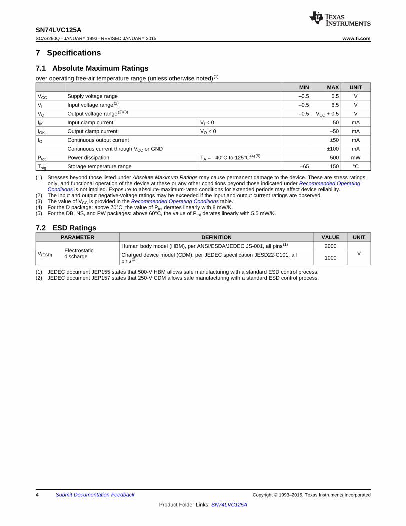
7 Specifications
7.1 Absolute Maximum Ratingsover operating free-air temperature range (unless otherwise noted) (1)
MIN MAX UNITVCC Supply voltage range –0.5 6.5 VVI Input voltage range (2) –0.5 6.5 VVO Output voltage range (2) (3) –0.5 VCC + 0.5 VIIK Input clamp current VI < 0 –50 mAIOK Output clamp current VO < 0 –50 mAIO Continuous output current ±50 mA
Continuous current through VCC or GND ±100 mAPtot Power dissipation TA = –40°C to 125°C (4) (5) 500 mWTstg Storage temperature range –65 150 °C
(1) Stresses beyond those listed under Absolute Maximum Ratings may cause permanent damage to the device. These are stress ratingsonly, and functional operation of the device at these or any other conditions beyond those indicated under Recommended OperatingConditions is not implied. Exposure to absolute-maximum-rated conditions for extended periods may affect device reliability.
(2) The input and output negative-voltage ratings may be exceeded if the input and output current ratings are observed.(3) The value of VCC is provided in the Recommended Operating Conditions table.(4) For the D package: above 70°C, the value of Ptot derates linearly with 8 mW/K.(5) For the DB, NS, and PW packages: above 60°C, the value of Ptot derates linearly with 5.5 mW/K.
7.2 ESD RatingsPARAMETER DEFINITION VALUE UNIT
Human body model (HBM), per ANSI/ESDA/JEDEC JS-001, all pins (1) 2000ElectrostaticV(ESD) VCharged device model (CDM), per JEDEC specification JESD22-C101, alldischarge 1000pins (2)
(1) JEDEC document JEP155 states that 500-V HBM allows safe manufacturing with a standard ESD control process.(2) JEDEC document JEP157 states that 250-V CDM allows safe manufacturing with a standard ESD control process.
4 Submit Documentation Feedback Copyright © 1993–2015, Texas Instruments Incorporated
Product Folder Links: SN74LVC125A

SN74LVC125Awww.ti.com SCAS290Q –JANUARY 1993–REVISED JANUARY 2015
7.3 Recommended Operating Conditionsover operating free-air temperature range (unless otherwise noted) (1)
TA = 25°C –40°C to 85°C –40°C to 125°CUNIT
MIN MAX MIN MAX MIN MAXOperating 1.65 3.6 1.65 3.6 1.65 3.6
VCC Supply voltage VData retention only 1.5 1.5 1.5VCC = 1.65 V to 1.95 V 0.65 × VCC 0.65 × VCC 0.65 × VCC
High-levelVIH VCC = 2.3 V to 2.7 V 1.7 1.7 1.7 Vinput voltageVCC = 2.7 V to 3.6 V 2 2 2VCC = 1.65 V to 1.95 V 0.35 × VCC 0.35 × VCC 0.35 × VCC
Low-levelVIL VCC = 2.3 V to 2.7 V 0.7 0.7 0.7 Vinput voltageVCC = 2.7 V to 3.6 V 0.8 0.8 0.8
VI Input voltage 0 5.5 0 5.5 0 5.5 VVO Output voltage 0 VCC 0 VCC 0 VCC V
VCC = 1.65 V –4 –4 –4VCC = 2.3 V –8 –8 –8High-levelIOH mAoutput current VCC = 2.7 V –12 –12 –12VCC = 3 V –24 –24 –24VCC = 1.65 V 4 4 4VCC = 2.3 V 8 8 8Low-levelIOL mAoutput current VCC = 2.7 V 12 12 12VCC = 3 V 24 24 24
Δt/Δv Input transition rise or fall rate 8 8 8 ns/V
(1) All unused inputs of the device must be held at VCC or GND to ensure proper device operation. Refer to the TI application report,Implications of Slow or Floating CMOS Inputs, literature number SCBA004.
7.4 Thermal InformationD (2) DB (2) NS (2) PW (2) RGY (3)
THERMAL METRIC (1) UNIT14 PINS
RθJA Junction-to-ambient thermal resistance 86 96 76 113 47 °C/W
(1) For more information about traditional and new thermal metrics, see the IC Package Thermal Metrics application report, SPRA953.(2) The package thermal impedance is calculated in accordance with JESD 51-7.(3) The package thermal impedance is calculated in accordance with JESD 51-5.
Copyright © 1993–2015, Texas Instruments Incorporated Submit Documentation Feedback 5
Product Folder Links: SN74LVC125A

SN74LVC125ASCAS290Q –JANUARY 1993–REVISED JANUARY 2015 www.ti.com
7.5 Electrical Characteristicsover recommended operating free-air temperature range (unless otherwise noted)
TA = 25°C –40°C to 85°C –40°C to 125°CPARAMETER TEST CONDITIONS VCC UNIT
MIN TYP MAX MIN MAX MIN MAX1.65 V toIOH = –100 μA VCC – 0.2 VCC – 0.2 VCC – 0.33.6 V
IOH = –4 mA 1.65 V 1.29 1.2 1.05IOH = –8 mA 2.3 V 1.9 1.7 1.55VOH V
2.7 V 2.2 2.2 2.05IOH = –12 mA
3 V 2.4 2.4 2.25IOH = –24 mA 3 V 2.3 2.2 2
1.65 V toIOL = 100 μA 0.1 0.2 0.33.6 VIOL = 4 mA 1.65 V 0.24 0.45 0.6
VOL VIOL = 8 mA 2.3 V 0.3 0.7 0.75IOL = 12 mA 2.7 V 0.4 0.4 0.6IOL = 24 mA 3 V 0.55 0.55 0.8
II VI = 5.5 V or GND 3.6 V ±1 ±5 ±20 μAIOZ VO = VCC or GND 3.6 V ±1 ±10 ±20 μAICC VI = VCC or GND, IO = 0 3.6 V 1 10 40 μA
One input at VCC – 0.6 V, 2.7 V toΔICC 500 500 5000 μAOther inputs at VCC or GND 3.6 VCi VI = VCC or GND 3.3 V 5 pF
7.6 Switching Characteristicsover recommended operating free-air temperature range (unless otherwise noted) (see Figure 3)
TA = 25°C –40°C to 85°C –40°C to 125°CFROM TOPARAMETER VCC UNIT(INPUT) (OUTPUT) MIN TYP MAX MIN MAX MIN MAX1.8 V ± 0.15 V 1 4.5 11.8 1 12.3 1 13.82.5 V ± 0.2 V 1 2.7 5.8 1 6.3 1 8.4
tpd A Y ns2.7 V 1 3 5.3 1 5.5 1 7
3.3 V ± 0.3 V 1 2.5 4.6 1 4.8 1 61.8 V ± 0.15 V 1 4.3 13.8 1 14.3 1 15.82.5 V ± 0.2 V 1 2.7 6.9 1 7.4 1 9.5
ten OE Y ns2.7 V 1 3.3 6.4 1 6.6 1 8.5
3.3 V ± 0.3 V 1 2.4 5.2 1 5.4 1 71.8 V ± 0.15 V 1 4.3 10.6 1 11.1 1 12.62.5 V ± 0.2 V 1 2.2 5.1 1 5.6 1 7.7
tdis OE Y ns2.7 V 1 2.5 4.8 1 5 1 6.5
3.3 V ± 0.3 V 1 2.4 4.4 1 4.6 1 6tsk(o) 3.3 V ± 0.3 V 1 1.5 ns
7.7 Operating CharacteristicsTA = 25°C
TESTPARAMETER VCC TYP UNITCONDITIONS1.8 V 7.4
Cpd Power dissipation capacitance per gate f = 10 MHz 2.5 V 11.3 pF3.3 V 15
6 Submit Documentation Feedback Copyright © 1993–2015, Texas Instruments Incorporated
Product Folder Links: SN74LVC125A

2
4
6
8
10
12
14
0 50 100 150 200 250 300
CL – Load Capacitance – pF
VCC = 3 V,
TA = 25°C
One Output Switching
Four Outputs Switching
t–
Pro
pag
ati
on
Dela
yT
ime
–n
sp
d
2
4
6
8
10
0 50 100 150 200 250 300
CL – Load Capacitance – pFt
–P
rop
ag
ati
on
De
lay
Tim
e–
ns
pd
VCC = 3 V,
TA = 25°C
One Output Switching
Four Outputs Switching
SN74LVC125Awww.ti.com SCAS290Q –JANUARY 1993–REVISED JANUARY 2015
7.8 Typical Characteristics
Figure 1. Propagation Delay (Low to High Transition) Figure 2. Propagation Delay (High to Low Transition)vs Load Capacitance vs Load Capacitance
Copyright © 1993–2015, Texas Instruments Incorporated Submit Documentation Feedback 7
Product Folder Links: SN74LVC125A

VM
thtsu
From Output
Under Test
CL
(see Note A)
LOAD CIRCUIT
S1
VLOAD
Open
GND
R
R
L
L
Data Input
Timing Input
VI
0 V
VI
0 V0 V
t
Input
w
VOLTAGE WAVEFORMS
SETUP AND HOLD TIMES
VOLTAGE WAVEFORMS
PROPAGATION DELAY TIMES
INVERTING AND NONINVERTING OUTPUTS
VOLTAGE WAVEFORMS
PULSE DURATION
tPLH
tPHL
tPHL
tPLH
VOH
VOH
VOL
VOL
VI
0 VInput
Output
Waveform 1
S1 at VLOAD
(see Note B)
Output
Waveform 2
S1 at GND
(see Note B)
VOL
VOH
tPZL
tPZH
tPLZ
tPHZ
VLOAD/2
0 V
VOL + V∆
VOH - V∆
≈0 V
VI
VOLTAGE WAVEFORMS
ENABLE AND DISABLE TIMES
LOW- AND HIGH-LEVEL ENABLING
Output
Output
tPLH/tPHL
tPLZ/tPZL
tPHZ/tPZH
Open
VLOAD
GND
TEST S1
NOTES: A. CL includes probe and jig capacitance.
B. Waveform 1 is for an output with internal conditions such that the output is low, except when disabled by the output control.
Waveform 2 is for an output with internal conditions such that the output is high, except when disabled by the output control.
C. All input pulses are supplied by generators having the following characteristics: PRR≤ 10 MHz, ZO = 50 Ω.
D. The outputs are measured one at a time, with one transition per measurement.
E. tPLZ and tPHZ are the same as tdis.
F. tPZL and tPZH are the same as ten.
G. tPLH and tPHL are the same as tpd.
H. All parameters and waveforms are not applicable to all devices.
Output
Control
V V
V V
V V
V
V V
V
V
V
V
M M
M M
M M
M
M M
M
M
M
I
VM
VM
1.8 V ± 0.15 V
2.5 V ± 0.2 V
2.7 V
3.3 V ± 0.3 V
1 kΩ
500 Ω
500 Ω
500 Ω
VCC RL
2 × VCC
2 × VCC
6 V
6 V
VLOAD CL
30 pF
30 pF
50 pF
50 pF
0.15 V
0.15 V
0.3 V
0.3 V
V
V
∆
CC
VCC
2.7 V
2.7 V
V
V
I
CC/2
VCC/2
1.5 V
1.5 V
VMt /tr f
≤2 ns
≤2 ns
≤2.5 ns
≤2.5 ns
INPUTS
SN74LVC125ASCAS290Q –JANUARY 1993–REVISED JANUARY 2015 www.ti.com
8 Parameter Measurement Information
Figure 3. Load Circuit and Voltage Waveforms
8 Submit Documentation Feedback Copyright © 1993–2015, Texas Instruments Incorporated
Product Folder Links: SN74LVC125A

2A 2Y
2OE
1A 1Y
1OE
4A 4Y
4OE
3A 3Y
3OE
SN74LVC125Awww.ti.com SCAS290Q –JANUARY 1993–REVISED JANUARY 2015
9 Detailed Description
9.1 OverviewThe SN74LVC125A device is a quadruple bus buffer gate featuring independent line drivers with 3-state outputs.Each output is disabled when the associated output-enable (OE) input is high. When OE is low, the respectivegate passes the data from the A input to its Y output. To ensure the high-impedance state during power up orpower down, OE should be tied to VCC through a pull-up resistor; the minimum value of the resistor is determinedby the current-sourcing capability of the driver.
9.2 Functional Block Diagram
9.3 Feature Description• Wide operating voltage range
– Operates from 1.65 V to 5.5 V• Allows down voltage translation• Inputs accept voltages to 5.5 V
9.4 Device Functional Modes
Table 1. Function TableINPUTS OUTPUT
YOE AL H HL L LH X Z
Copyright © 1993–2015, Texas Instruments Incorporated Submit Documentation Feedback 9
Product Folder Links: SN74LVC125A

C or System Logic 1A
4A
1Y
4Y
VCC
GND
C/System Logic/LEDs
3 V5 V
1OE
4OE
SN74LVC125ASCAS290Q –JANUARY 1993–REVISED JANUARY 2015 www.ti.com
10 Application and Implementation
NOTEInformation in the following applications sections is not part of the TI componentspecification, and TI does not warrant its accuracy or completeness. TI’s customers areresponsible for determining suitability of components for their purposes. Customers shouldvalidate and test their design implementation to confirm system functionality.
10.1 Application InformationSN74LVC125A is a high drive CMOS device that can be used for a multitude of bus interface type applicationswhere output drive or PCB trace length is a concern. The inputs can accept voltages to 5.5 V at any valid VCCmaking it ideal for down translation.
10.2 Typical Application
Figure 4. Typical Application Schematic
10.2.1 Design RequirementsThis device uses CMOS technology and has balanced output drive. Care should be taken to avoid buscontention because it can drive currents that would exceed maximum limits. The high drive will also create fastedges into light loads so routing and load conditions should be considered to prevent ringing.
10.2.2 Detailed Design Procedure1. Recommended Input Conditions:
– For rise time and fall time specifcations, see (Δt/ΔV) in the Recommended Operating Conditions table.– For specified high and low levels, see (VIH and VIL) in the Recommended Operating Conditions table.– Inputs are overvoltage tolerant allowing them to go as high as (VI max) in the Recommended Operating
Conditions table at any valid VCC.2. Recommend Output Conditions:
– Load currents should not exceed (IO max) per output and should not exceed (Continuous current throughVCC or GND) total current for the part. These limits are located in the Absolute Maximum Ratings table.
10 Submit Documentation Feedback Copyright © 1993–2015, Texas Instruments Incorporated
Product Folder Links: SN74LVC125A

–100
–80
–60
–40
–20
0
20
40
60
–1 –0.5 0.0 0.5 1.0 1.5 2.0 2.5 3.0 3.5 4.0
TA = 25°C, VCC = 3 V,
VIH = 3 V, VIL = 0 V,
All Outputs Switching
VOH – V
I OH
–m
A
VOL – V
–20
0
20
40
60
80
100
–0.2 0.0 0.2 0.4 0.6 0.8 1.0 1.2 1.4 1.6
TA = 25°C, VCC = 3 V,
VIH = 3 V, VIL = 0 V,
All Outputs Switching
I OL
–m
A
SN74LVC125Awww.ti.com SCAS290Q –JANUARY 1993–REVISED JANUARY 2015
Typical Application (continued)– Outputs should not be pulled above VCC.– Series resistors on the output may be used if the user desires to slow the output edge signal or limit the
output current.
10.2.3 Application Curves
Figure 5. Output Drive Current (IOL) Figure 6. Output Drive Current (IOH)vs LOW-level Output Voltage (VOL) vs HIGH-level Output Voltage (VOH)
11 Power Supply RecommendationsThe power supply can be any voltage between the MIN and MAX supply voltage rating located in theRecommended Operating Conditions table.
Each VCC terminal should have a good bypass capacitor to prevent power disturbance. For devices with a singlesupply, a 0.1 μF capacitor is recommended. If there are multiple VCC terminals then 0.01 μF or 0.022 μFcapacitors are recommended for each power terminal. It is ok to parallel multiple bypass capacitors to rejectdifferent frequencies of noise. Multiple bypass capacitors may be paralleled to reject different frequencies ofnoise. The bypass capacitor should be installed as close to the power terminal as possible for the best results.
12 Layout
12.1 Layout GuidelinesWhen using multiple bit logic devices, inputs should not float. In many cases, functions or parts of functions ofdigital logic devices are unused. Some examples are when only two inputs of a triple-input AND gate are used,or when only 3 of the 4-buffer gates are used. Such input pins should not be left unconnected because theundefined voltages at the outside connections result in undefined operational states.
Specified in Figure 7 are rules that must be observed under all circumstances. All unused inputs of digital logicdevices must be connected to a high or low bias to prevent them from floating. The logic level that should beapplied to any particular unused input depends on the function of the device. Generally they will be tied to GNDor VCC, whichever makes more sense or is more convenient.
Copyright © 1993–2015, Texas Instruments Incorporated Submit Documentation Feedback 11
Product Folder Links: SN74LVC125A

VCC
Unused Input
Input
Output Output
Input
Unused Input
SN74LVC125ASCAS290Q –JANUARY 1993–REVISED JANUARY 2015 www.ti.com
12.2 Layout Example
Figure 7. Layout Diagram
12 Submit Documentation Feedback Copyright © 1993–2015, Texas Instruments Incorporated
Product Folder Links: SN74LVC125A

SN74LVC125Awww.ti.com SCAS290Q –JANUARY 1993–REVISED JANUARY 2015
13 Device and Documentation Support
13.1 TrademarksAll trademarks are the property of their respective owners.
13.2 Electrostatic Discharge CautionThese devices have limited built-in ESD protection. The leads should be shorted together or the device placed in conductive foamduring storage or handling to prevent electrostatic damage to the MOS gates.
13.3 GlossarySLYZ022 — TI Glossary.
This glossary lists and explains terms, acronyms and definitions.
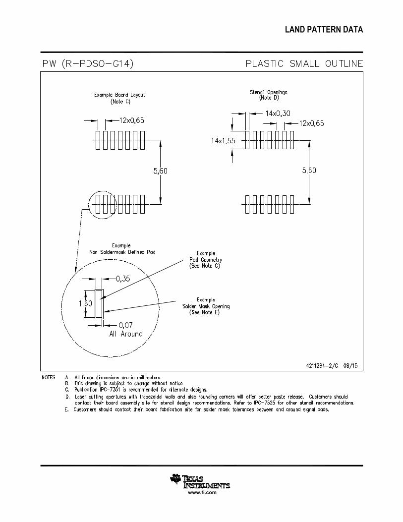
14 Mechanical, Packaging, and Orderable InformationThe following pages include mechanical packaging and orderable information. This information is the mostcurrent data available for the designated devices. This data is subject to change without notice and revision ofthis document. For browser based versions of this data sheet, refer to the left hand navigation.
Copyright © 1993–2015, Texas Instruments Incorporated Submit Documentation Feedback 13
Product Folder Links: SN74LVC125A

PACKAGE OPTION ADDENDUM
www.ti.com 10-Dec-2020
Addendum-Page 1
PACKAGING INFORMATION
Orderable Device Status(1)
Package Type PackageDrawing
Pins PackageQty
Eco Plan(2)
Lead finish/Ball material
(6)
MSL Peak Temp(3)
Op Temp (°C) Device Marking(4/5)
Samples
SN74LVC125AD ACTIVE SOIC D 14 50 RoHS & Green NIPDAU Level-1-260C-UNLIM -40 to 125 LVC125A
SN74LVC125ADBR ACTIVE SSOP DB 14 2000 RoHS & Green NIPDAU Level-1-260C-UNLIM -40 to 125 LC125A
SN74LVC125ADBRG4 ACTIVE SSOP DB 14 2000 RoHS & Green NIPDAU Level-1-260C-UNLIM -40 to 125 LC125A
SN74LVC125ADE4 ACTIVE SOIC D 14 50 RoHS & Green NIPDAU Level-1-260C-UNLIM -40 to 125 LVC125A
SN74LVC125ADG4 ACTIVE SOIC D 14 50 RoHS & Green NIPDAU Level-1-260C-UNLIM -40 to 125 LVC125A
SN74LVC125ADR ACTIVE SOIC D 14 2500 RoHS & Green NIPDAU | SN Level-1-260C-UNLIM -40 to 125 LVC125A
SN74LVC125ADRE4 ACTIVE SOIC D 14 2500 RoHS & Green NIPDAU Level-1-260C-UNLIM -40 to 125 LVC125A
SN74LVC125ADRG3 ACTIVE SOIC D 14 2500 RoHS & Green SN Level-1-260C-UNLIM -40 to 125 LVC125A
SN74LVC125ADRG4 ACTIVE SOIC D 14 2500 RoHS & Green NIPDAU Level-1-260C-UNLIM -40 to 125 LVC125A
SN74LVC125ADT ACTIVE SOIC D 14 250 RoHS & Green NIPDAU Level-1-260C-UNLIM -40 to 125 LVC125A
SN74LVC125ADTG4 ACTIVE SOIC D 14 250 RoHS & Green NIPDAU Level-1-260C-UNLIM -40 to 125 LVC125A
SN74LVC125ANSR ACTIVE SO NS 14 2000 RoHS & Green NIPDAU Level-1-260C-UNLIM -40 to 125 LVC125A
SN74LVC125APW ACTIVE TSSOP PW 14 90 RoHS & Green NIPDAU Level-1-260C-UNLIM -40 to 125 LC125A
SN74LVC125APWE4 ACTIVE TSSOP PW 14 90 RoHS & Green NIPDAU Level-1-260C-UNLIM -40 to 125 LC125A
SN74LVC125APWG4 ACTIVE TSSOP PW 14 90 RoHS & Green NIPDAU Level-1-260C-UNLIM -40 to 125 LC125A
SN74LVC125APWR ACTIVE TSSOP PW 14 2000 RoHS & Green NIPDAU | SN Level-1-260C-UNLIM -40 to 125 LC125A
SN74LVC125APWRE4 ACTIVE TSSOP PW 14 2000 RoHS & Green NIPDAU Level-1-260C-UNLIM -40 to 125 LC125A
SN74LVC125APWRG3 ACTIVE TSSOP PW 14 2000 RoHS & Green SN Level-1-260C-UNLIM LC125A
SN74LVC125APWRG4 ACTIVE TSSOP PW 14 2000 RoHS & Green NIPDAU Level-1-260C-UNLIM -40 to 125 LC125A
SN74LVC125APWT ACTIVE TSSOP PW 14 250 RoHS & Green NIPDAU Level-1-260C-UNLIM -40 to 125 LC125A

PACKAGE OPTION ADDENDUM
www.ti.com 10-Dec-2020
Addendum-Page 2
Orderable Device Status(1)
Package Type PackageDrawing
Pins PackageQty
Eco Plan(2)
Lead finish/Ball material
(6)
MSL Peak Temp(3)
Op Temp (°C) Device Marking(4/5)
Samples
SN74LVC125APWTE4 ACTIVE TSSOP PW 14 250 RoHS & Green NIPDAU Level-1-260C-UNLIM -40 to 125 LC125A
SN74LVC125APWTG4 ACTIVE TSSOP PW 14 250 RoHS & Green NIPDAU Level-1-260C-UNLIM -40 to 125 LC125A
SN74LVC125ARGYR ACTIVE VQFN RGY 14 3000 RoHS & Green NIPDAU Level-2-260C-1 YEAR -40 to 125 LC125A
(1) The marketing status values are defined as follows:ACTIVE: Product device recommended for new designs.LIFEBUY: TI has announced that the device will be discontinued, and a lifetime-buy period is in effect.NRND: Not recommended for new designs. Device is in production to support existing customers, but TI does not recommend using this part in a new design.PREVIEW: Device has been announced but is not in production. Samples may or may not be available.OBSOLETE: TI has discontinued the production of the device.
(2) RoHS: TI defines "RoHS" to mean semiconductor products that are compliant with the current EU RoHS requirements for all 10 RoHS substances, including the requirement that RoHS substancedo not exceed 0.1% by weight in homogeneous materials. Where designed to be soldered at high temperatures, "RoHS" products are suitable for use in specified lead-free processes. TI mayreference these types of products as "Pb-Free".RoHS Exempt: TI defines "RoHS Exempt" to mean products that contain lead but are compliant with EU RoHS pursuant to a specific EU RoHS exemption.Green: TI defines "Green" to mean the content of Chlorine (Cl) and Bromine (Br) based flame retardants meet JS709B low halogen requirements of <=1000ppm threshold. Antimony trioxide basedflame retardants must also meet the <=1000ppm threshold requirement.
(3) MSL, Peak Temp. - The Moisture Sensitivity Level rating according to the JEDEC industry standard classifications, and peak solder temperature.
(4) There may be additional marking, which relates to the logo, the lot trace code information, or the environmental category on the device.
(5) Multiple Device Markings will be inside parentheses. Only one Device Marking contained in parentheses and separated by a "~" will appear on a device. If a line is indented then it is a continuationof the previous line and the two combined represent the entire Device Marking for that device.
(6) Lead finish/Ball material - Orderable Devices may have multiple material finish options. Finish options are separated by a vertical ruled line. Lead finish/Ball material values may wrap to twolines if the finish value exceeds the maximum column width.
Important Information and Disclaimer:The information provided on this page represents TI's knowledge and belief as of the date that it is provided. TI bases its knowledge and belief on informationprovided by third parties, and makes no representation or warranty as to the accuracy of such information. Efforts are underway to better integrate information from third parties. TI has taken andcontinues to take reasonable steps to provide representative and accurate information but may not have conducted destructive testing or chemical analysis on incoming materials and chemicals.TI and TI suppliers consider certain information to be proprietary, and thus CAS numbers and other limited information may not be available for release.
In no event shall TI's liability arising out of such information exceed the total purchase price of the TI part(s) at issue in this document sold by TI to Customer on an annual basis.

PACKAGE OPTION ADDENDUM
www.ti.com 10-Dec-2020
Addendum-Page 3
OTHER QUALIFIED VERSIONS OF SN74LVC125A :
• Automotive: SN74LVC125A-Q1
• Enhanced Product: SN74LVC125A-EP
NOTE: Qualified Version Definitions:
• Automotive - Q100 devices qualified for high-reliability automotive applications targeting zero defects
• Enhanced Product - Supports Defense, Aerospace and Medical Applications
TAPE AND REEL INFORMATION
*All dimensions are nominal
Device PackageType
PackageDrawing
Pins SPQ ReelDiameter
(mm)
ReelWidth
W1 (mm)
A0(mm)
B0(mm)
K0(mm)
P1(mm)
W(mm)
Pin1Quadrant
SN74LVC125ADBR SSOP DB 14 2000 330.0 16.4 8.35 6.6 2.4 12.0 16.0 Q1
SN74LVC125ADR SOIC D 14 2500 330.0 16.8 6.5 9.5 2.1 8.0 16.0 Q1
SN74LVC125ADR SOIC D 14 2500 330.0 16.4 6.5 9.0 2.1 8.0 16.0 Q1
SN74LVC125ADR SOIC D 14 2500 330.0 16.4 6.5 9.0 2.1 8.0 16.0 Q1
SN74LVC125ADRG3 SOIC D 14 2500 330.0 16.8 6.5 9.5 2.3 8.0 16.0 Q1
SN74LVC125ADRG4 SOIC D 14 2500 330.0 16.4 6.5 9.0 2.1 8.0 16.0 Q1
SN74LVC125ADRG4 SOIC D 14 2500 330.0 16.4 6.5 9.0 2.1 8.0 16.0 Q1
SN74LVC125ADT SOIC D 14 250 330.0 16.4 6.5 9.0 2.1 8.0 16.0 Q1
SN74LVC125ANSR SO NS 14 2000 330.0 16.4 8.2 10.5 2.5 12.0 16.0 Q1
SN74LVC125APWR TSSOP PW 14 2000 330.0 12.4 6.9 5.6 1.6 8.0 12.0 Q1
SN74LVC125APWR TSSOP PW 14 2000 330.0 12.4 6.9 5.6 1.6 8.0 12.0 Q1
SN74LVC125APWRG3 TSSOP PW 14 2000 330.0 12.4 6.9 5.6 1.6 8.0 12.0 Q1
SN74LVC125APWRG4 TSSOP PW 14 2000 330.0 12.4 6.9 5.6 1.6 8.0 12.0 Q1
SN74LVC125APWT TSSOP PW 14 250 330.0 12.4 6.9 5.6 1.6 8.0 12.0 Q1
SN74LVC125ARGYR VQFN RGY 14 3000 330.0 12.4 3.75 3.75 1.15 8.0 12.0 Q1
PACKAGE MATERIALS INFORMATION
www.ti.com 3-Aug-2021
Pack Materials-Page 1

*All dimensions are nominal
Device Package Type Package Drawing Pins SPQ Length (mm) Width (mm) Height (mm)
SN74LVC125ADBR SSOP DB 14 2000 853.0 449.0 35.0
SN74LVC125ADR SOIC D 14 2500 364.0 364.0 27.0
SN74LVC125ADR SOIC D 14 2500 340.5 336.1 32.0
SN74LVC125ADR SOIC D 14 2500 853.0 449.0 35.0
SN74LVC125ADRG3 SOIC D 14 2500 364.0 364.0 27.0
SN74LVC125ADRG4 SOIC D 14 2500 853.0 449.0 35.0
SN74LVC125ADRG4 SOIC D 14 2500 340.5 336.1 32.0
SN74LVC125ADT SOIC D 14 250 210.0 185.0 35.0
SN74LVC125ANSR SO NS 14 2000 853.0 449.0 35.0
SN74LVC125APWR TSSOP PW 14 2000 853.0 449.0 35.0
SN74LVC125APWR TSSOP PW 14 2000 364.0 364.0 27.0
SN74LVC125APWRG3 TSSOP PW 14 2000 364.0 364.0 27.0
SN74LVC125APWRG4 TSSOP PW 14 2000 853.0 449.0 35.0
SN74LVC125APWT TSSOP PW 14 250 853.0 449.0 35.0
SN74LVC125ARGYR VQFN RGY 14 3000 853.0 449.0 35.0
PACKAGE MATERIALS INFORMATION
www.ti.com 3-Aug-2021
Pack Materials-Page 2
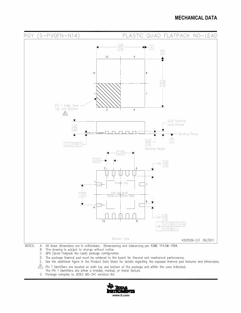


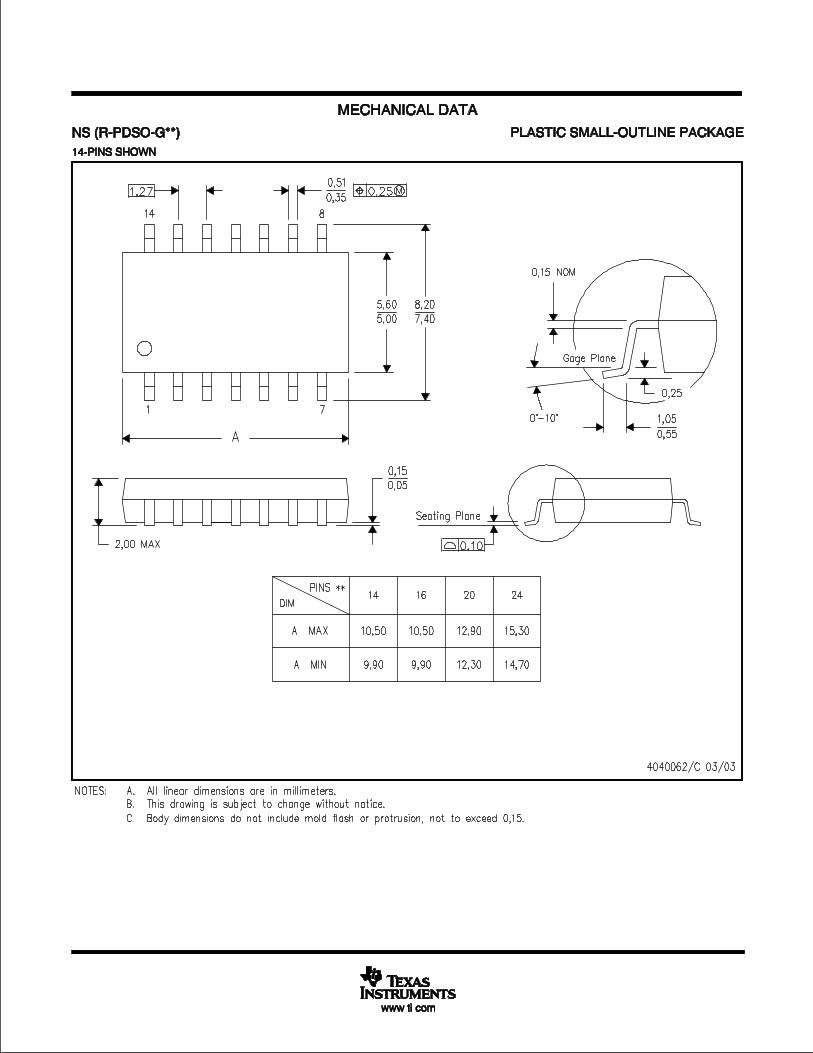


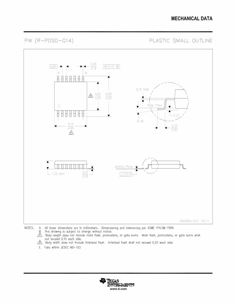

MECHANICAL DATA
MSSO002E – JANUARY 1995 – REVISED DECEMBER 2001
POST OFFICE BOX 655303 • DALLAS, TEXAS 75265
DB (R-PDSO-G**) PLASTIC SMALL-OUTLINE
4040065 /E 12/01
28 PINS SHOWN
Gage Plane
8,207,40
0,550,95
0,25
38
12,90
12,30
28
10,50
24
8,50
Seating Plane
9,907,90
30
10,50
9,90
0,38
5,605,00
15
0,22
14
A
28
1
2016
6,506,50
14
0,05 MIN
5,905,90
DIM
A MAX
A MIN
PINS **
2,00 MAX
6,90
7,50
0,65 M0,15
0°–8°
0,10
0,090,25
NOTES: A. All linear dimensions are in millimeters.B. This drawing is subject to change without notice.C. Body dimensions do not include mold flash or protrusion not to exceed 0,15.D. Falls within JEDEC MO-150

IMPORTANT NOTICE AND DISCLAIMERTI PROVIDES TECHNICAL AND RELIABILITY DATA (INCLUDING DATASHEETS), DESIGN RESOURCES (INCLUDING REFERENCEDESIGNS), APPLICATION OR OTHER DESIGN ADVICE, WEB TOOLS, SAFETY INFORMATION, AND OTHER RESOURCES “AS IS”AND WITH ALL FAULTS, AND DISCLAIMS ALL WARRANTIES, EXPRESS AND IMPLIED, INCLUDING WITHOUT LIMITATION ANYIMPLIED WARRANTIES OF MERCHANTABILITY, FITNESS FOR A PARTICULAR PURPOSE OR NON-INFRINGEMENT OF THIRDPARTY INTELLECTUAL PROPERTY RIGHTS.These resources are intended for skilled developers designing with TI products. You are solely responsible for (1) selecting the appropriateTI products for your application, (2) designing, validating and testing your application, and (3) ensuring your application meets applicablestandards, and any other safety, security, or other requirements. These resources are subject to change without notice. TI grants youpermission to use these resources only for development of an application that uses the TI products described in the resource. Otherreproduction and display of these resources is prohibited. No license is granted to any other TI intellectual property right or to any third partyintellectual property right. TI disclaims responsibility for, and you will fully indemnify TI and its representatives against, any claims, damages,costs, losses, and liabilities arising out of your use of these resources.TI’s products are provided subject to TI’s Terms of Sale (https:www.ti.com/legal/termsofsale.html) or other applicable terms available eitheron ti.com or provided in conjunction with such TI products. TI’s provision of these resources does not expand or otherwise alter TI’sapplicable warranties or warranty disclaimers for TI products.IMPORTANT NOTICE
Mailing Address: Texas Instruments, Post Office Box 655303, Dallas, Texas 75265Copyright © 2021, Texas Instruments Incorporated