introduction - virginia techjgtront/ece4540/project/... · web viewthere are 2 sections to this...
TRANSCRIPT

Project Grading
Level of Difficulty /5
Floor Plan /5
Gate Level Schematic /5
Block Level Drawing /5
Technical Description /15
Connection Diagram (Pin out diagram) /5
Check Plot(s) /10
SPICE Simulation /15
Gate/System Simulation (timing analysis) /10
Recommended Testing information /5
Overall Likelihood of Correctness /10
Overall Quality /10
TOTAL _____

Fall 2005 ECE 4540 Design Project
Error Detection and Correction Integrated Circuit Creation
ECE 4540 Design Project
Fall 2005
12/8/05
Page 2 of 33

Fall 2005 ECE 4540 Design Project
TABLE OF CONTENTS
Introduction 3
Gate & System Level Circuits and Layout 4
2-Input AND w/ one inverted input 42-1 Multiplexer 6Positive Edge Triggered D Flip-Flop 82-Input XOR Gate 104-Input XOR Gate 12
Pin Diagram 14
Floor Plan of Layout 15
Full Chip Layout with Package Frame 16
Full Chip Layout 17
Floor Plan Explanation 18
Location of Cadence Layout Files 18
Simulations & Testing 19
2-Input AND w/ one inverted input 192-1 Multiplexer 20Positive Edge Triggered D Flip-Flop 222-Input XOR Gate 234-Input XOR Gate 24
Timing Analysis 27
Test Plan 29
Conclusion 31
Page 3 of 33

Fall 2005 ECE 4540 Design Project
INTRODUCTION
This VLSI Design Project involved creating the simulation, layout, and test procedure for an Error Detection and Correction (EDAC) integrated circuit. The creation of this design established a general understanding of the necessary steps that must take place in the development of an integrated circuit. The general purpose of this circuit is to read the parity of an incoming digital word and generate an output flag when a parity error has occurred. When errors in parity have occurred, the circuit will correct them with the proper parity. The circuit includes 4 input exclusive OR gates, 2 input exclusive OR gates, AND gates, multiplexers, and D Flip Flops. Also to be included is a flip flop register for the 8 input signals. The finished project includes gate and system level diagrams of the chip, a chip pin diagram, a chip floor plan, layouts of the individual gate components, SPICE simulations, and a testing procedure. The layout must fit in a 40 pin package that is 2.2mm X 2.2mm.
The general procedure for the completion of this project first involved finding circuits for each of the necessary components. Each of these gate circuits were then simulated for functionality in PSpice. Upon proving that they were indeed correct, each gate was drawn in layout using optimization techniques from class. HSpice simulations were then run on the individual gate layouts. The timing and delay information was easily extracted from the HSpice data. Each gate was then connected together to complete the full chip design. The package frame was added at the end and each of the inputs and outputs of the circuit were wired to it. Lastly, a test procedure was developed to ensure that the complete chip worked as it was intended.
Page 4 of 33
Fall 2005 ECE 4540 Design Project
GATE & SYSTEM LEVEL CIRCUITS AND LAYOUT
2-Input AND w/ one inverted input
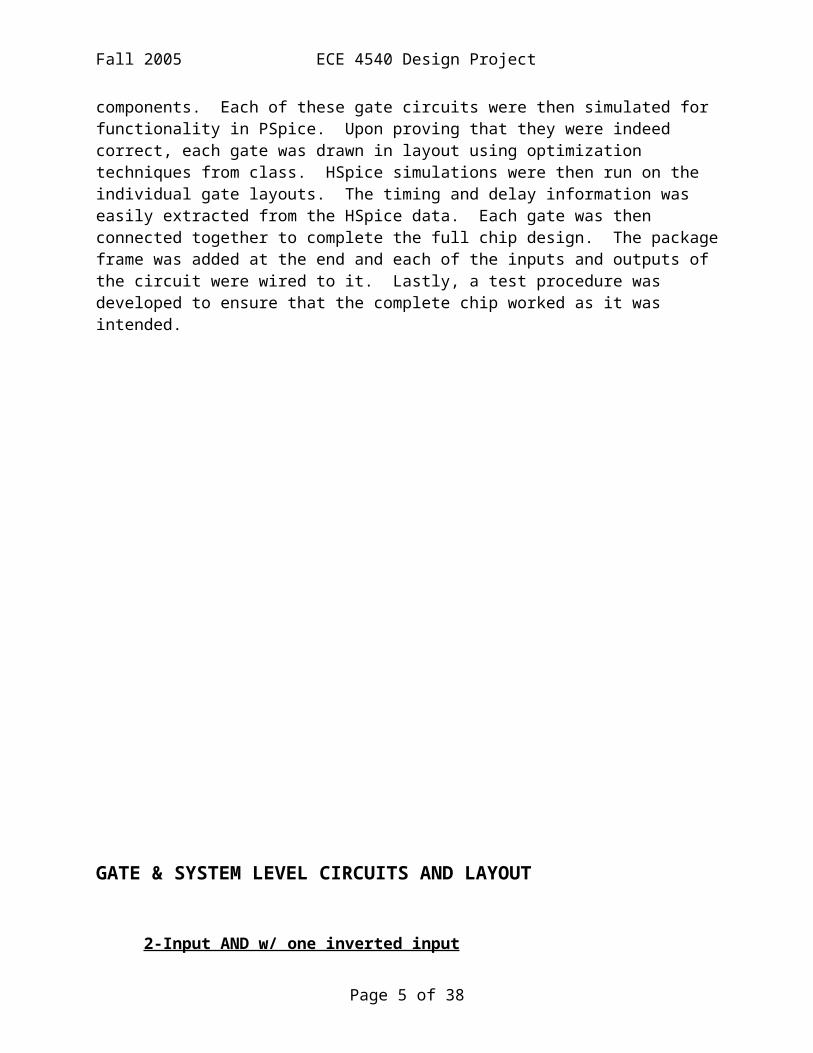
The figure below is the transistor level circuit of the 2-input AND gate which is one of the components of the EDAC.
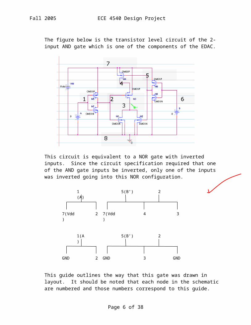
This circuit is equivalent to a NOR gate with inverted inputs. Since the circuit specification required that one of the AND gate inputs be inverted, only one of the inputs was inverted going into this NOR configuration.
This guide outlines the way that this gate was drawn in layout. It should be noted that each node in the schematic are numbered and those numbers correspond to this guide.
Page 5 of 33
7(Vdd)
5(B’)
4
2
3
5(B’)
3
2
GNDGND
1 (A)
7(Vdd) 2
GND
1(A)
2
Fall 2005 ECE 4540 Design Project
Each of the arrows going down to a node name is a source or drain and the arrow going up in between is a gate connection.
The layout for the AND gate was drawn according to the simulations that verified its operation. The n-devices and the p-devices are spread out so that their separation matches all of the other gates. It is thought that having all of the rails line up and connected together was a good design practice.
Page 6 of 33

Fall 2005 ECE 4540 Design Project
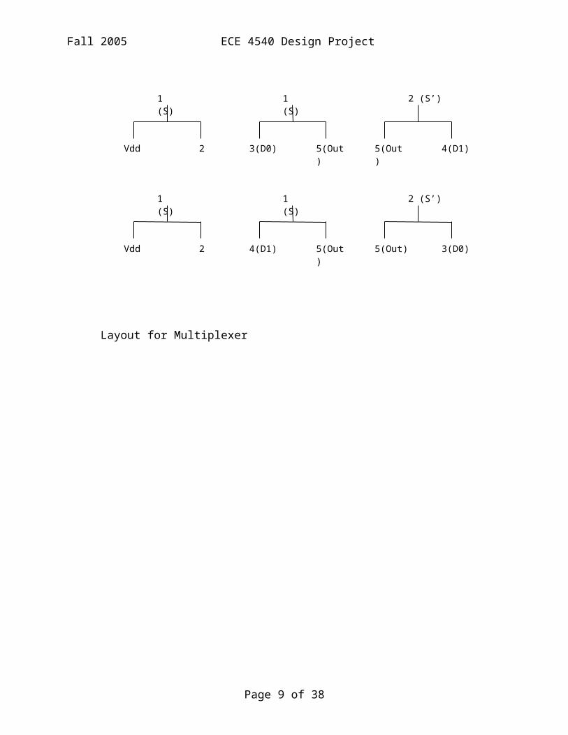
2-1 Multiplexer
The figure below is the transistor level circuit for the 2-1 multiplexer which is also used to realize the EDAC.
The multiplexer is simply an inverter for the control signal and a pair of transmission gates. The control signal selects which transmission gate is on and therefore the input signal that passes to the output.
Layout Guide for Multiplexer
Page 7 of 33
1 (S)
Vdd 2
1 (S)
Vdd 2
1 (S)
3(D0) 5(Out)
1 (S)
2 (S’)
4(D1)
2 (S’)
3(D0)5(Out)
5(Out)
5(Out)4(D1)

Fall 2005 ECE 4540 Design Project
Layout for Multiplexer
Page 8 of 33
Fall 2005 ECE 4540 Design Project
Positive Edge Triggered D Flip-Flop
This gate design uses a combination of transmission gates and NOR gates to provide buffered outputs.
Layout Guide for D Flip-Flop
Page 9 of 33
Vdd 2
1
10
5
Vdd 5
4
Vdd 7
6
Vdd 8
7
3 4
1
2
10 5 6
2 1
8
Gnd 2
1
10
5
Gnd 5
4
Gnd 7
6
Gnd 8
7
10 4
1
2
3 8 6
2 1
5

Fall 2005 ECE 4540 Design Project
Page 10 of 33

Fall 2005 ECE 4540 Design Project
2-Input XOR Gate
There are 2 sections to this design: the 4 transistor gate and the 4 transistor buffer. The buffer is necessary to restore the signal of the gate section. The pull-up portion of the gate connects the transistor sources to the opposite transistor gates. The pull-down portion is connected in series and tied to the GND rail.
Gate Schematic
M 7M b re a k N
M 1 6M b re a k N
0
M 1 7
M b re a k P
M 1 8
M b re a k P
5 . 0 0 0 V
0 V5 . 00 0 V
M 9
M b re a k P
M 4M b re a k N
0
5 2 8 . 5m V
M 1 0
M b re a k P
M 5M b re a k N
5 . 0 0 0 V
5 . 0 0 0 V5 . 0 0 0V
5 . 0 0 0 V
V 1 05 V d c
VV
V 5
TD = 1 0 n s
TF = 0 . 5 n sP W = 1 0 n sP E R = 2 0 n s
V 1 = 0 V d c
TR = 0 . 5 n s
V 2 = 5 V d c
0
V 65 V d c
0
0 0 V
Page 11 of 33

Fall 2005 ECE 4540 Design Project
Gate Layout for 2-Input XOR
Page 12 of 33

Fall 2005 ECE 4540 Design Project
4-Input XOR Gate
The 4-Input XOR gate uses 3 2-Input XORs cascaded together with a buffer. This gate used the previously mentioned 2-Input XOR design with the same model parameters and channel widths and lengths.
Gate Level Schematic Using 2-Input XORs
B C
A
D2
3 1
U 1 A
7 4 1 2 8
56 4
U 1 B
7 4 1 2 8
89 1 0
U 1 C
7 4 1 2 8
Transistor Level Schematic
M 7M b re a k N
M 1 6M b re a k N
0
M 1 7
M b re a k P
M 1 8
M b re a k P
0 V
4 . 5 3 1 V
5 . 0 0 0 V
0
5 .0 0 0 V
V 1 05 V d c
V 5
TD = 1 0 n s
TF = 0 .1 n sP W = 1 0 n sP E R = 2 0 n s
V 1 = 0 V d c
TR = 0 .1 n s
V 2 = 5 V d c
0
M 9
M b re a k p
M 4M b re a k n
7 . 4 9 0 n V
M 1 0
M b re a k P
M 5M b re a k N
5 .0 0 0 V
5 .0 0 0 V7 . 4 9 0 n V
0
5 . 0 0 0 V
V 65 V d c
0 V0
M 8M b re a k N
M 1 9M b re a k N
M 2 0
M b re a k P
M 2 1
M b re a k P
2 2 .4 7 n V
5 . 0 0 0 V5 .0 0 0 V
0
5 .0 0 0 V
V 1 15 V d c
0
5 . 0 0 0 V
M 1 1M b re a k N
M 2 2M b re a k N
M 2 3
M b re a k P
M 2 4
M b re a k P
4 . 5 3 1 V
4 4 .9 4 n V5 .0 0 0 V
0
5 .0 0 0 V
V 1 25 V d c
0
4 4 .9 4 n V
5 .0 0 0 V
V
V
Page 13 of 33

Fall 2005 ECE 4540 Design Project
Page 14 of 33

Fall 2005 ECE 4540 Design Project
PIN DIAGRAM
Page 15 of 33
P3 P1 P4 P2 VDD P5 HOLD’ TP1 SHIFT
TP4 BPAR EV/OD’ PGEN GND TP3 NC NC NC
B7
B6
B5
B4
B3
B2
B1
B0
I. Enable
NC
NC
S-IN
TP2
PARERR’
PARERR
EN’
CLK
NC
Note:NC = Not ConnectedTP1 = Left MUX OutTP2 = Right MUX OutTP3 = AND OutTP4 = 4 XORS Out
HOKIES 2449

Fall 2005 ECE 4540 Design Project
FLOOR PLAN OF LAYOUT
Page 16 of 33
2
1
3
4
5
6
4 5
3 2
6
1
7
0
3
5
2
4
1
6
MUX MUX
D Flip Flop
4-input XOR
2-input XOR
2-input AND
2-1 MUX

Fall 2005 ECE 4540 Design Project
Full Layout with Package Frame
Page 17 of 33

Fall 2005 ECE 4540 Design Project
Page 18 of 33

Fall 2005 ECE 4540 Design Project
Page 19 of 33

Fall 2005 ECE 4540 Design Project
FLOORPLAN EXPLANATION
The chip was put together in this way so that each of the parts would flow into the next stage of the circuit. The gates were made so that the rails were equal distances apart and all of the rails would line up in the overall floor plan. The general idea behind the structure of the whole chip was that the 8 B Inputs would come in from the left and the outputs of the circuit would come out on the right. Therefore, each gate was added according to its order in line in the circuit. The input flip flop register is first on the left, then the 4 Input XOR gates, then the 2 Input XOR and the AND gates, and lastly the Multiplexers. This strategy kept long running metal lines to a minimum as many of the connections were close to each other. There are 2 rows of gates with the bottom row being normal alignment (n-well on top and nMOS on the bottom) and the top row is mirrored vertically. This allows for one long solid n-well, which is believed to ease manufacturing if this chip were to be made. This also allows for a large contiguous VDD area in the middle of many signal lines to provide a little signal shielding.
LOCATION OF CADENCE LAYOUT FILES
The layout files for this project can be found in the following directory after logging into any of the UNIX machines in the workstation lab. The privilege levels of the files have been modified so that the files can be accessible.
/home/abbash/ece4540/VLSI_Final_Project
Please note that once in cadence these files are under the VLSI_Final_Project folder.
Page 20 of 33

Fall 2005 ECE 4540 Design Project
SIMULATIONS & TESTING
2-Input AND w/ one inverted input
AB OUT
The truth table for this gate is as follows:Input A Input B Output
0 0 00 1 01 0 11 1 0
The figure below shows the HSpice simulations for this gate. As you can see, the output is only asserted when is input A is high and input b is low.
Page 21 of 33

Fall 2005 ECE 4540 Design Project
2-1 Multiplexer
The truth table for this logic gate is as follows:
S I1 I0 Output0 0 0 0(I0)0 0 1 1(I0)0 1 0 0(I0)0 1 1 1(I0)1 0 0 0(I1)1 0 1 0(I1)1 1 0 1(I1)1 1 1 1(I1)
The figure below is our HSpice simulations for the multiplexer we laid out. As the simulation indicates, the output depends on the input which is selected from the select line.
Multiplexer Simulation
Page 22 of 33
I0
I1S
OutMUX

Fall 2005 ECE 4540 Design Project
Positive Edge Triggered D Flip-Flop
Page 23 of 33

Fall 2005 ECE 4540 Design Project
D
C
QDATA
CLK
OUT
The D flip-flop is a time synchronous device. In this project the flip-flop is positive edge triggered. On a low to high transition of the clock the output is updated. Simulation results of our D flip-flop layout are shown in the following figure.
2-Input XOR Gate
Page 24 of 33

Fall 2005 ECE 4540 Design Project
BA OUT
The truth table for this gate is as follows:
Input A Input B Output0 0 00 1 11 0 11 1 0
This gate gives an output of ‘1’ when the there is an odd number of active high ‘1’ inputs. Output simulations for our layout for this gate are shown in the following figure.
4-Input XOR Gate
Page 25 of 33

Fall 2005 ECE 4540 Design Project
BA
DC OUT
A B C D Output0 0 0 0 00 0 0 1 10 0 1 0 10 0 1 1 00 1 0 0 10 1 0 1 00 1 1 0 00 1 1 1 11 0 0 0 11 0 0 1 01 0 1 0 01 0 1 1 11 1 0 0 01 1 0 1 11 1 1 0 11 1 1 1 0
The HSpice simulation results for our 4-input XOR gate are shown on the following page. All possible combinations on inputs are outputs are shown.
Page 26 of 33

Fall 2005 ECE 4540 Design Project
Page 27 of 33

Fall 2005 ECE 4540 Design Project
Full Chip Simulation
D0D1D2D3
S0S1
EN
Q D
C
Q
DEV2
01
01
01
01
01
01
01
01
01
01
01
01
01
01
01
D0D1D2D3
S0S1
EN
Q
P2
P1
P4
P3
BPAR
EV/OD'
PGEN
P5
EN'
HOLD'
S-IN
SHIFT
CLK
PARERR
0
3
6
5
7
4
2
1
Page 28 of 33

Fall 2005 ECE 4540 Design Project
TIMING ANALYSIS
D Flip-Flops: Maximum Rise Time of Output = (2.5 – 1.6) ns
= 0.9 ns
Maximum Fall Time of Output = (10502 – 10501) ns= 1 ns
Maximum Delay = (10.502 – 10.501) us= 1.0 ns
2-Input AND w/ one inverted input:Maximum Rise Time of Output = (3001.6 – 3000.7) ns
= 0.7 ns
Maximum Fall Time of Output = (501.7 – 501.1) ns= 0.6 ns
Maximum Delay = (0.97 – 0.25) ns= 0.72 ns
2-1 Multiplexer:Maximum Rise Time of Output = (504.0 – 503.1) ns
= 0.9 ns
Maximum Fall Time of Output = (4.1 – 3.3) ns= 0.8 ns
Maximum Delay = (1503.82 – 1503.00) ns= 0.82 ns
2-Input XOR GateMaximum Delay = (1503.82 – 1503.00) ns
= 0.82 ns
4-Input XOR GateMaximum Rise Time of Output = (108.07-107.68) ns
= 0.4 ns
Maximum Fall Time of Output = (109.2-108.4) ns= 0.8 ns
Maximum Delay = (12 - 7) ns= 5 ns
Page 29 of 33

Fall 2005 ECE 4540 Design Project
Maximum Frequency Calculations
Time for Longest Path to Output = (5 + 5 + 0.72 + 0.82 + 0.82 + 1) ns= 13.36 ns = 13.4 ns (approx)
Therefore maximum frequency for this circuit = 1 / Longest Path to Output= 1 / (13.4 ns)= 74.6 MHz
Page 30 of 33

Fall 2005 ECE 4540 Design Project
TEST PLAN
The test plan can be divided into 3 sections so that parts of the circuit that are not involved do not slow down the testing time. Test points have been included to aid in detection of errors in the circuit.
The parity outputs are directly based on the conditions of the 8 inputs. Therefore, a simple input scan can check the functionality of the parity outputs. The inputs not listed in this section can remain static as they do not affect the outputs of this section.
All of the other B Inputs beside B0 and B1 should remain at logic 0 (GND) for testing this section. The other inputs can remain static.
This section requires probing the pins PGEN and S-IN in order to determine if the outputs are correct. In this section, the B Inputs can remain static.
Page 31 of 33

Fall 2005 ECE 4540 Design Project
CONCLUSION
Page 32 of 33

Fall 2005 ECE 4540 Design Project
This project demonstrated the necessary steps of creating an integrated circuit from a basic gate schematic. There were several trade-offs involved, many of which were on the gate level. For example, there were a few variations on the minimal XOR configuration. The original 16 transistor 4 input XOR gate that was implemented did not work for all states in the initial simulations, thus requiring an alternative to be found. This fact brought out the importance of simulation at multiple levels of chip design.
The large frame allowed for much freedom in the layout of the full chip. A quick calculation of areas revealed that our string of gates only used 5% of the total area within the package frame. The wires connecting the internal gates to the package frame were made as wide as possible so that the resistance was minimized and the overall chip speed could be as fast as possible.
Much of this design could have been enhanced for various reasons, but due to the freedom of the package size, number of pins, speed, and power, these perfections were disregarded. Given more time, this design could have been improved both in circuit design as well as layout, but this current design is more than sufficient given the requirements and guidelines.
Page 33 of 33