smt magazine, july 2014
TRANSCRIPT


4 SMT Magazine • July 2014
Since the EU passed the Restriction of Hazardous Substances directive in 2006, tin whiskers have become a serious threat to the assembly of PCBs. This month, our feature contributors Dr. Jennie Hwang, Andrzej Czerwinski, and Linda Woody tackle this prickly subject.
Tin Whiskers: Capsulizationby Dr. Jennie S. Hwang
Whisker Growth in Tin Alloys on Glass-Epoxy laminateby A. Czerwinski, A. Skwarek, M. Płuska, J. Ratajczak and K. Witek
Tin Whisker Risk Management by Conformal Coatingby Linda Woody and William Fox
16 30
40


6 SMT Magazine • July 2014
C o n t e n t s
JULy 2014
voLUME 29
nUMBER 7
www.smtmagazine.com
EnginEERing
SoLUTionS
foR PCB
MAnUfACTURing
ArticleMeeting Future Stencil Printing Challenges with ultrafine Powder Solder Pastesby Edward Briggs
columnsElectronic Assembly with Solder: an unblinking look at “The Devil We Know”by Joe Fjelstad
DFARS Flow Downs and Trusted Suppliersby Todd Kramer
More Stencil Questions (and the Answers!)by Rachel Miller-Short
news highlightsMil/Aero
Market
Supplier/New Product
SMTonline
76
8
62
70
60
68
74
90
Video interViewsMajor Changes in the last Eight Decades
A Glimpse of the Future
DEK Deals with Automotive Device Miniaturization
shortEfficient Thermal Cooling and Heating
extrAsEvents Calendar
Advertiser Index & Masthead
15
66
73
88
92
93


8 SMT Magazine • July 2014
ing electronic assemblies of every sort. The only fly in the ointment is that the EU parliament, in a mad rush to try to look “green,” took the emotional and scientifically ill-advised position that lead needed to be banned from electronic solders.
Sadly, there was never presented a credible piece of scientific evidence that any user had ever been harmed by tin-lead solder in elec-tronic equipment. Nor could they prove their
assertion that it would be a risk to ground water. That
said, it is true that greed and com-plete mismanage-ment of electronic waste boarding on
criminal behavior, has resulted in physical illness and environ-mental harm in areas of the world where
Solder is unquestionably highly practical technology for joining metals, and carries with it a long history. Its roots go back more than 2,000 years. Somewhere in the distant past, one of our more clever and observant ancestors chanced to create an alloy of tin and lead that melted at a low temperature. They or someone who learned of their discovery found that this unique combination of elements could be used to join pieces of metal together. This combina-tion of chance observation and applied imagination has proven a key devel-opment in the tech-nological history of mankind. Those in the electronics industry of today are very familiar with this ancient tech-nology and today it is still the method of choice for mak-
by Joe FjelstadvERDAnT ELECTRoniCS
ElECTRoNIC INTERCoNNECTIoNS
gUEST CoLUMn
Electronic Assembly with Solder: an unblinking look at “The Devil We Know”

We put our people first, because they are our greatest asset!
When you join the Hunter team, you become part of an organization that prides itself on putting people first. If you enjoy an exciting, fast-paced work environment combined with a family-like atmosphere, the Hunter team might be the place for you!
With facilities in Milpitas, CA and Atlanta, GA, we’re always looking for people to add to our 45-year history of manufacturing excellence!
+1 (408) 957-1300 www.hunter-technology.com
VIEW OUR OPEN POSITIONS »

10 SMT Magazine • July 2014
uncontrolled recycling was being carried out by uneducated individuals. While all is not yet well in that regard, that “hole” in the system is being addressed by businesses, NGOs and gov-ernments around the world.
Not to be forgotten is the fact that the im-pact of the EU’s decision has been significant and far-reaching and it has caused the industry to spend needlessly many tens of billions of dol-lars diverting the considerable talents of count-less talented engineers and scientists around the world to make products that are unfortunately proving less reliable and arguably less environ-mentally friendly electronics than those built with tin lead solders.
The Devil We Know, Disrobed While soldering (especially tin-lead solder-
ing) holds many benefits in terms of offering a means of mass assembly of electronic com-ponents to printed circuit boards and is funda-mentally simple, its application in the assembly and manufacture of electronic products of the present age is much more complex and fraught with opportunity for defects to be generated, but it is also the a demon we have elected to live with, for as the old saying suggests that “Bet-ter is the devil we know.” The devil we know is at least familiar and the simple truth is that humans are creatures of habit and most of us abhor change. There is a lingering question in the current situation? Is dealing with the devil we know on a daily basis really worth the price we are paying?
Following is a recitation of some of the many types of solder and solder-related defects that test and inspection is tasked with finding before a product reaches market. Bear in mind as these defects are recounted and reviewed that the cost of defects rises as a product moves fur-ther from the manufacturing line.
a) Opens: Opens are discontinuities gener-ated in the soldering process that can be mani-fest in assembly in a number of ways. For exam-ple, a bent or lifted lead on a QFP component, missing solder ball on a BGA, insufficient solder on an LGA or the warpage of the component during the high-temperature, lead-free reflow process can all result in an open circuit.
b) Shorts: Solder shorts are bridges of sol-der between one or more component leads on an assembly. As component lead pitch con-tinues to drop, the incidence of short circuits increases. Presently, the threshold of pain for most assembly is experienced when the lead pitch drops below 0.5 mm.
c) Insufficient Solder: Insufficient solder is a condition where the amount of solder in a solder joint is less than desired or specified con-tractually through industry specifications or customer requirements.
d) Excessive Solder: Excessive solder is obviously the opposite of the condition of in-sufficiency and is again measured against agree-ments. It also introduces a wild card because it is not what reliability testing is based on.
e) Solder Cracking: Solder cracking is an obvious concern as it could result in a la-tent open circuit condition. Good during prod-uct test before shipping but then failing in the field.
f) Tin Whiskers: Tin whiskers are small metal projections emanating from a solder joint. They can grow up to 15 mm long and given the fine pitch of today’s components, they are a significant concern. There are also challenging because they are typically a latent defect that shows up unpredictably. Past research indicat-ed that the addition of lead to tin solder alloys would mitigate the formation of whiskers; how-ever, with the ban on lead in electronic solders the incidence of whiskers is on the rise.
g) Poor Wetting/Dewetting: Good wet-ting is manifest by the presence of uniform coat of solder on both the leads of the compo-nent and terminations of the printed circuit to which they are joined. In areas of poor wetting or dewetting the solder thins appreciably in ar-eas leaving only a thin silvery sheen.
h) Voids: Voids are defect which are often difficult to detect without use of special equip-ment such as an X-ray apparatus. The chal-lenge with voids is that they represent potential weakness in the solder joint owing to their in-consistent nature. Voids can be found both in through-hole and surface mount components. In the case of surface mount components the voids are often extremely small and are some-times referred to as champagne voids.
ELECTRoniC inTERConnECTionS
ElECTRoNIC ASSEMBly WITH SolDER continues

July 2014 • SMT Magazine 11
ELECTRoniC inTERConnECTionS
ElECTRoNIC ASSEMBly WITH SolDER continues
i) Blowholes: A term applied to a phenom-enon where a small hole is observed in a solder joint. Typically, the defect is found to be the result of discontinuities in the plated through-hole wall, which may absorb flux and then ex-plosively out gas during the soldering process.
j) Cold Solder Joints: Solder joints that did not form completely a good metallurgical bond. They are often the result of the joint receiving sufficient heat to cause complete melting and joining of the solder. Cold solder joints are of-ten seen in cases where the component lead is connected to a large thermally conductive fea-ture or element and insufficient heat is retained near the lead to assure a good solder joint. With lead-free solders, the phenomenon pro-vides a greater challenge as the amount of heat which must be supplied is much greater than it might have been with a tin lead solder, thus potentially degrading device and assem-bly reliability.
k) Brittle Solder Joints: Solder joints wherein the al-loy formed in the soldering process due to dissolution of elements within the finish or on the circuit board (e.g., gold), results in a solder joint that is less ductile than the solder used in the assembly process.
l) Head-on-Pillow: A new type of defect which was identified only with the introduc-tion of lead-free soldering. It is an unsettling type of defect in that it is not easily detected but could result in an intermittent open in the operation of the assembly. The term was chosen because the phenomenon is reminiscent of an individual’s head forming a depression on a pil-low.
m) Graping: Another lead-free related de-fect wherein the small, often ball-like particles of solder in a solder paste do not reflow com-pletely, leaving a surface that looks like the sur-face of a bunch of grapes. Like head-in-pillow, it is a defect that may not be easily detected.
n) Tombstoning: Tombstoning is a term that has been applied to the appearance of a de-
fect related to discrete devices such as resistors and capacitors, wherein solder connections are not made simultaneously; the slight lag causes the first side to reflow to pull back and rotate up, resembling a grave marker (which is somewhat apropos given that the assembly will likely be dead if tombstones are present).
o) Component Cracking: Component cracking can have multiple causes, one being a situation where there is a significant mismatch in terms of coefficient of thermal expansion be-tween the component and the printed circuit to which it is attached. It can also occur if the
assembly is flexed in the area of the component, causing the device to
crack.p) Popcorning: Popcorn-
ing is a phenomenon mani-fest when moisture entrapped within a component outgases during assembly, causing a blister to form in the encapsu-lation material. With the ad-vent of lead-free soldering and its higher temperatures, the incidence of popcorning rises and in fact moisture sensitiv-ity levels of components are degraded to reflect the new reality.
q) Solder Balling: Solder balling is a condition which hap-
pens during the reflow of a solder paste on a surface mount assembly. It is a result of the high temperature of reflow causing rapid volatility station of the flux and spatter of the solder particles that are part of the flux. While a viable solder joint may be created even as solder balls are being formed, they represent a risk to the long term reliability of the assembly as po-tential shorting elements.
r) Misregistration: Components with fine pitch leads, if jostled before or during the assem-bly, may be misregistered relative to the land pattern, resulting in a nonfunctional product.
s) Insufficient Cleaning Under Devic-es: As mentioned previously, insufficient clean-ing under surface mount devices can result in latent failure through the formation of high re-sistance shorts or the growth of dendrites.
Component cracking can have multiple
causes, one being a situation where there is a significant mismatch in terms of coefficient of thermal expansion
between the component and the printed circuit to
which it is attached.
“
”

12 SMT Magazine • July 2014
Clearly there is a great deal of nuance in the detection and identification of solder related de-fects; numerous books have been written over the last few decades that both characterize and suggest methods for eliminating or mitigating them (the devil is also “in the details” as anoth-er aphorism attests). It is not within the scope of this brief commentary to provide detail on all of the various types of solder related defects
which can extend from the macro to the micro but for the benefit of the reader the following figure is offered providing representative ex-amples of a number of the defects described above.
The “Devil’s” Impact on the PCB
The importance of managing the soldering process is clear, but making a good solder joint is also just part of the story and there are a number of defects that can be generated within a printed circuit assembly because of the soldering process, including:
a) Corner Cracking: A crack that forms at the interface between the whole and the land that sur-rounds. It is normally the result of the Z-axis expansion of the PCB during the thermal excursions such as soldering.
b) Barrel Cracking: Another phenomenon associated with the soldering process; it is similar in some ways to a corner crack except that it is manifest near the center of the hole.
c) Post Separation: A separa-tion of the plating in the through hole from an innerlayer connection
d) Hole-Wall Pull Away: Hole-wall pull away is manifest as a bulge in a plated through hole, which reduces its diameter.
e) Resin Recession: Roughly, the opposite of hole-wall pull away wherein a small gap is formed be-
tween the plated hole wall and a resin rich area of a plated through-hole
f) Delamination: A separation of the lay-ers of a multilayer circuit. It is normally seen in cases where the glass transition temperature of the resins used in the multilayer structure is exceeded.
g) Pad Cratering: Another phenomenon unseen before the introduction of lead-free sol-
ELECTRoniC inTERConnECTionS
ElECTRoNIC ASSEMBly WITH SolDER continues
figure 1: Representative images of some of the solder related defect found on printed circuit assemblies. Top row – left to right: head in pillow, graping, misregistration short and over-heated flux. Second row, left to right: tombstoning, insufficient solder with open, popcorning. Third row, left to right: dewet-ting, blowhole, shorting between adjacent leads. fourth row, left to right: cracked solder joints, voids, excessive solder. Bot-tom row, left to right: cracked component, tin whisker, open (lifted lead).


14 SMT Magazine • July 2014
dering. It is manifest as a circumferential tear of the copper land to which a component, nor-mally a BGA, is assembled.
h) Decomposition: Decomposition of a PCB is a relatively new phenomenon associated with higher temperatures used with lead-free soldering. In fact, a new term was added to the industry lexicon, Td, which is the temperature of decomposition representing a loss of a specified percentage of the weight of the printed circuit.
Clearly, printed circuit technology, like sol-dering technology, is fraught with its own vul-nerabilities due to the complexities of process-ing. The demands on PCB technology foisted upon the industry by the imposition of lead-free soldering requirements have placed a heavy bur-den on the printed circuit manufacturing indus-try. The need for higher glass transition tempera-tures to assure a measure of survival through the elevated temperatures of lead-free soldering has required the printed circuit industry to qualify new materials. Simultaneously, there has been a demand placed upon the industry to remove halogenated flame retardants from its materials. This double-barreled challenge is one that the industry had not faced before. Moreover, the in-dustry has been challenged to provide circuits with ever-finer features which operate at ever-increasing frequencies.
To their credit, printed circuit industry tech-nologist, engineers and scientists have struggled admirably to address these challenges, includ-ing the challenge of finding solutions to defect modalities that were unknown to the industry just a few years ago. Unfortunately, a number of the defects described are related to solder-ing and its effects. The earlier problems have been exacerbated by the increased temperature required for lead-free soldering. Figure 2 offers cross-sections of representative printed circuit defects resulting from thermal excursions.
Solderless Assembly for Electronics (SAFE) Technology: A Simpler Approach?
Given all the challenges and risks associated with soldering, every thoughtful and prudent manufacturing engineer must constantly be seeking a way or ways to make assembly pro-cessing more robust. If one looks for inspiration
on how they might end their dealing with the devil, they can find it in the Bible, where it is written: “If thine eye offend thee, pluck it out, and cast it from thee.” Perhaps this is a bit ex-treme, but this seems to be where the industry is stuck today in dealing with the devil. Solder is by analogy an offending element of manufac-turing and source of many if not most manufac-turing problems. The industry will continue to have to deal with that devil as long as we persist in its use.
One can do their own research to test this assertion if they choose. They need look no fur-
ELECTRoniC inTERConnECTionS
ElECTRoNIC ASSEMBly WITH SolDER continues
figure 2: Cross-sectional micrographs of printed circuit defects caused by soldering are provided above. Clockwise from the upper left-hand cor-ner: corner crack, barrel crack , pad lifting, post separation, pad cratering ,hole wall pull away, resin recession and delamination.
July 2014 • SMT Magazine 15
ELECTRoniC inTERConnECTionS
ElECTRoNIC ASSEMBly WITH SolDER continues
verdant Electronics founder and President Joseph (Joe) fjelstad is a four-decade veteran of the electronics industry and an inter-national authority and innovator in the field of electronic inter-connection and packaging tech-
nologies. fjelstad has more than 250 U.S. and international patents issued or pending and is the author of flexible Circuit Technology.
ther than the titles of papers in publications. Presently, this and other industry/academic journals and proceedings on electronic manu-facturing are rife with articles, papers, commen-taries and advertisements offering new materi-als, processes and equipment both for manu-facture and inspection to try and beat lead-free solder into submission. Unfortunately, solder appears a wily and crafty adversary that always seems to offer another challenge to each new solution proposed. This situation begs the ques-tion: “Is there any alternative?” The answer, in the opinion of this author, is “Yes.” The answer is to assemble electronics without solder.
The potential benefits of eliminating solder is significant in many areas of current concern or high interest in electronic manufacturing, including: cost , reliability, performance, envi-ronmental impact, design security, a means of addressing some elements of counterfeiting, sustainability, a means of sidestepping conflict metals concerns and others.
So how can it be done? It is really quite simple:
Build assemblies in reverse and instead of placing and joining components on circuit boards with solder, build up circuits on “component boards” using copper plating, thereby bypassing the sol-dering process completely along with all of its many extra processing steps, ongoing challenges, and problems. The potential economic, environ-mental and reliability benefits are substantial as will be shown. The concept of SAFE assembly and its practicality will be examined in more detail in a future paper. SMT
realtimewith.comCliCk
To View
Video Interview
guest Editor Dan feinberg and indium’s Rick Short enjoy a wide-ranging conversation that includes the evolution of the SMT industry throughout the past 80 years, and Short’s 30 years with indium.
Major Changes in the last Eight Decadesby Real Time with...IPC APEX EXPO 2014

16 SMT Magazine • July 2014
by Dr. Jennie S. HwangH-TECHnoLogiES gRoUP
fEATURE
Since lead-free implementation, concerns about tin whiskers have intensified. For the past 12 years, studies and research by various laboratories and organizations have delivered burgeoning reports and papers, and my column has devoted an entire series to this subject. This article aims to capsulize the important areas of the subject. (Note: For expression, “whisker” is used as both noun and verb.)
The tin whisker issue and its potential mis-haps have been recognized for more than six decades in electronic, electrical and industrial applications. Some metals are prone to whisker-ing, or protruding from the surface of the sub-strate. In addition to tin, the metals that have exhibited whiskers include zinc, cadmium, sil-ver, gold, aluminum, copper, lead, and others.
The whiskering phenomenon is distinct and unique. It is the result of a process differ-ent from other known phenomena (e.g., den-
drites). And tin whisker and tin pest are separate metallurgical phenomena (SMT Magazine, May 2013). However, whiskers share commonality with dendrites in two aspects: Both are the re-sult of a physical metallurgical process, thus fol-lowing the science of physical metallurgy; and both could cause a product failure.
Uncertainty about tin whisker growth is most insidious. Stock markets do not like un-certainty, nor does the electronics industry. Our effort is to alleviate the uncertainty.
Practical CriteriaAs some metals can whisker when accom-
modating conditions are met, the goal should be set with the differentiation between whisker-resistant and whisker-proof.
Overall, for testing or evaluation of the whisker propensity of a system, the key ques-tions to be addressed are, is the system whisker-prone or whisker-resistant (not whisker-proof), and how does the system’s whisker resistance stand in reference to the intended benchmark?
Tin Whiskers: Capsulization


18 SMT Magazine • July 2014
To comply with RoHS regulations, Pb-free materials including pure tin (Sn) have been used as surface coating for component leads and metal terminals, and Sn-based alloys as sol-der materials in making solder joints. Because of its economics, availability, manufacturability, compatibility and solderability, pure tin makes a practical replacement for Sn-Pb as a choice of surface coating. Today, most component manu-facturers offer pure tin-coated components.
The evaluation of tin whisker propensity and growth rate needs to be put in the context of relative formation rate under a set of conditions. For the electronic and electrical applications, the renewed concern about tin whiskers are largely the result of conversion from tin-lead coating to lead-free (or tin coating) for component leads or PCB surface finish. Thus, the relative perfor-mance in reference to a tin-lead benchmark that has demonstrated satisfactory whisker-resistance is a logical criterion, not the absolute perfor-mance. An SAC (SnAgCu) alloy is lead-free, but a lead-free alloy is not necessarily an SAC. This clarity is particularly important as more viable lead-free alloys become commercially available. And tin whiskering is highly sensitive to an alloy composition including impurities.
Phenomena and observationsTin whisker reflects its coined name, which
has long been recognized to be associated with electroplated tin coating and most likely occurs with pure tin. Its appearance resembles whiskers. However, they can also form in a wide range of shapes and sizes, such as fibrous filament-like spirals, nodules, columns and mounds (Figure 1). Tin whiskers are often single crystals and electrically conductive. They are normally brit-tle in nature but can be rendered ductile when whiskers are very long and thin.
Whisker formation and its resulting shapes and sizes depend on time, temperature, sub-strate, surface condition of the substrate, sur-face morphology, plating chemistry, and plat-ing process. The rate of whisker growth also depends on a list of factors including the above-mentioned.
Whiskers sometimes grow up to a few mm long, but usually less than 50 µm, and a few mi-crons in diameter. Whiskers may grow, but they
may also be self-annihilating as the electric cur-rent can fuse the whisker if the current is suffi-cient (e.g., typically more than 50 milliamps is often required). The self-annihilation ability var-ies with the whisker’s size in length and diameter. This self-annihilating occurrence further contrib-utes to the observed inconsistent or mythical na-ture of the events. Furthermore, the highly dis-parate whisker growth rates have been reported, ranging from 0.03 to 9 mm/year. And whiskers can grow even in a vacuum environment.
Among various findings, one experiment indicated that whiskers can be eliminated by controlling the plating process in an equiva-lent way to controlling stresses in materials. The very sharp decrease in internal stress of tin electrodeposits was observed after plating as quickly as within minutes. It is interesting to note that this fast stress release occurs regardless whether initial stress in the deposit is compres-sive or tensile. In the case of compressive or ten-sile stress, the value of the stress drops to very low numbers, but it remains being of the same type as the initial stress form (i.e., high initial tensile stress reduces to much lower stress value but remains tensile and high compressive stress remains compressive).
It has been observed that the inclusion of organic elements in the tin structure promote tin growth. Organic inclusion or the level of in-clusion is in turn affected by the plating chem-istry[1,2]. And bright tin has exhibited to be most susceptible to whisker formation. Bright tin
TIN WHISKERS: CAPSulIzATIoN continues
fEATURE
figure 1: Tin whiskers appearance, from mound to filament.

July 2014 • SMT Magazine 19
plating chemistry is prone to creating an envi-ronment that creates greater organic inclusion and higher stress level in tin crystal structure. The nature of substrate, external mechanical force, and temperature have been found to af-fect tin whiskering as well.
Concerns and potential impactIf/when tin whisker occurs, concerns and
impact primarily fall in the following four cat-egories (SMT Magazine, November 2013).
1. Short circuitsWhen a whisker grows to a length that bridg-
es the adjacent lead or terminal, this conductive whisker can cause an electrical short. However, if a whisker is formed but does not bridge its neighbor, there will not be an electrical short. To complicate the phenomena, there are occa-sions where whiskers may not cause failure, or a failure may not be detected even when the whisker physically touch the adjacent lead due to lack of electrical current flow.
2. Tin metal arcingUnder high levels of current and voltage
that is able to vaporize the whisker and ion-
ize the metal gas, metal arc can occur. A NASA report attributed a satellite failure to tin metal vapor arc as the suspected root cause. It is ex-pected that tin arc is more likely to occur under reduced atmospheric pressures or vacuum envi-ronments.
3. Break-off debrisThe whiskers, being brittle and conductive,
can break off from the base of its substrate sur-face, which may create functional issues. This is particularly a concern for sensitive electronic devices, such as optical and computer disk driv-er applications. The break-off behavior varies with the service conditions and the characteris-tics of the whisker.
4. Unwanted antennaTin whiskers can act like miniature anten-
nas, which affect the circuit impedance and cause reflections. In this case, the most affected areas are in high-frequency applications (higher than 6 GHz) or in fast digital circuits.
Causes and Contributing FactorsRegarding causes and factors, physical met-
allurgy is the place to go to. Fundamentally, tin
TIN WHISKERS: CAPSulIzATIoN continues
fEATURE
figure 2: Tin whiskers—organic inclusions and grain size (four months aged at 50°C).

20 SMT Magazine • July 2014
whisker follows the basic physical metallurgy in its principles on nucleation and crystal growth through the classic theories of dislocation dy-namics and of other lattice defects in tin crys-tal structure. Thus, for whiskers to appear from the tin-based (or coated) surface, the causes and contributing factors should be intimately related to the nucleation site creation and the subsequent growth paths. However, the actual processes of nucleation and grain growth of tin whisker are dauntingly complex.
The nucleation and growth can be encour-aged by stresses introduced during and after the plating process. The sources of these stresses come from multiple fronts. This includes re-sidual stresses caused by electroplating and/or additional stresses imposed after plating, and/or the induced stresses by foreign elements, and/or thermally-induced stresses. Specific causes and contributing factors are excerpted from my previous article (SMT Magazine, March 2014):
organic InclusionsOrganic inclusions affect the tin crystal
structure by distorting or crowding the crystal lattice, thus creating the internal stress. It is found that tin whisker growth is correlated to the organic inclusions as represented in carbon content in the coating. A test conducted at 50°C for four months on coatings that have simi-
TIN WHISKERS: CAPSulIzATIoN continues
lar grain sizes generated the following results: 235 µm whisker was formed from the coating containing 0.2% carbon; 12 µm whisker was formed from the coating containing 0.05% car-bon content[1,2].
Surface Physical ConditionSurface conditions, such as notches or
scratches on the surface, are the source of atom-ic irregularity, which could contribute to the driving force of tin whisker formation.
Substrate Surface MorphologyPhysically maneuvering the surface mor-
phology of the substrate in the level of rough-ness was found to alter the tin whisker propen-sity—a rougher surface being less prone to tin whiskers[3], as shown in Figure 3. It is believed that a relatively rougher surface facilitates the formation of an even interface between the tin coating and the substrate surface that contains a thinner and more uniform intermetallic layer.
oxidation or Contamination levelIt is postulated that as the oxygen atoms
diffuse into tin crystal structure, oxygen can serve as nuclei and can also restrain grain boundary mobility and diffusion. When the lattice structure is oriented in a way that is favorable to the protruding crystal growth,
fEATURE
figure 3: Tin whiskers—role of surface morphology (chemical micro-roughening to produce a set of surface roughness with specific Ra values).

July 2014 • SMT Magazine 21
TIN WHISKERS: CAPSulIzATIoN continues
fEATURE
tin whiskers will occur. Other studies found that surface oxide promotes tin whiskers[1,2] and surface corrosion and contamination also contribute to tin whiskers[4,5]. It was also found that whisker growth occurred on SAC305 solder joints on either the copper or the alloy 42 leaded components, and the al-loy 42 leads exhibited a delay in long whisker growth[4,5].
External Mechanical StressesExternally applied forces such as those
introduced by the lead-forming, bending or torque after plating process may affect tin whisker formation. In studying the effect of external mechanical force that is imposed on the coating on tin whisker growth, the rela-tive whisker growth under different levels of organic inclusions with and without an exter-nal mechanical force were performed. Under each level of organic inclusions, an external mechanical force (by the means of bending) created an increased rate of whisker growth as shown in Table 1 below[1].
Substrate Base MaterialIt was found that there is a difference in tin
whisker propensity between bronze and brass[6] and between Cu-based and alloy 42 leads, re-spectively. The differences are primarily attrib-uted to relative inter-diffusion between the sub-strate material and the tin-based materials, as well as to the relative abundance of intermetal-lic compounds.
Metallic ImpuritiesAs metallic particles enter into the tin lat-
tice, there may or may not lead to the forma-tion of intermetallic compounds, depending on the metallurgy of the elements involved. These metallic particles can change or distort the lat-tice spacing in the tin structure.
Intermetallic CompoundsIt should be emphasized that intermetallic
compounds at the interface of tin coating and the substrate or in the bulk of the tin-based ma-terial is not necessary for tin whiskers to form.
However, intermetallic compounds may ex-ert additional effects in grain structure, as these compounds can form in various geometries and morphologies ranging from small, more-round-ed particles to long needles. This formation cre-ates either high localized stress or well-distribut-ed stress or both in the tin lattice structure.
It should also be noted that the critical dif-ference between SnPb and SnAgCu alloy is that SnPb does not (should not) form intermetallics in the bulk matrix, but SnAgCu alloys intrin-sically contain intermetallics. The presence of intermetallics in SnAgCu and the absence of such in SnPb account for most of phenomenal and property differences between SnAgCu and SnPb, including tin whisker.
CTE Mismatch Between Tin Coating and Substrate
The relative coefficient of thermal expan-sion between the tin plating and substrate can contribute to the occurrence of tin whisker as the result of additional global stress as well as localized stresses. In this regard, the lead mate-rial (e.g., alloy 42 vs. Cu) is a factor. Although the larger mismatch between the tin layer and the substrate causes higher stress levels, the dif-fusion rate of substrate atoms into the tin-based material layer with or without the companion of the formation of intermetallics may skew the linear relationship between CTE mismatch and whisker propensity.
Plating Process vs. Coating Surface Morphology
Tin plating process parameters control the lattice defects incorporated in the tin layer. It
Table 1.
organic Impurity No Mechanical Bend Mechanical Bend
0.2%, 4 months 245 microns 312 microns
0.004%, 7 months 6 microns 6 microns

22 SMT Magazine • July 2014
also determines the thickness of the coating layer. The organic content, grain size, and sur-face morphology highly depend on the coating chemistry and process parameters, including the type of electrolyte, additive/brighteners, current density, process temperature, and the process control. For instance, high current den-sity allows faster rate of plating, and a faster rate may impede the tin atoms’ ability to rearrange to a low-energy state, which contributes to sub-sequent whiskering conditions.
Take bright tin as an example, which is re-portedly the most susceptible to tin whisker. Its high susceptibility is largely attributable to the high residual stresses within the tin plating caused by the plating chemistry and process. The added brighteners in making tin bright may serve as nucleation sites and may prevent tin from settling into the low energy state to form large grains. The resulting small grains provide more grain boundaries that in turn offer diffu-sion paths for tin.
Plating Process vs. Coating Crystal Structure
The effect of microstructure in terms of grain size on whiskers has been observed—equi-axed crystal structure (Type C in Figures 4 and 5) and thin IMC minimizes whiskers[3]. It is hypothe-sized that as grain size reduces below 1 micron,
the internal stress and the driving force for re-crystallization will be built up. This condition creates high whisker propensity.
Thickness of Tin CoatingIt is postulated that it takes a proper thick-
ness for whiskers to grow. To make a statement on the correlation between the thickness of tin layer and the whisker propensity is indeed over-simplistic. Yet, some results do support that a too thick coating can bury whiskering tendency and a too thin coating can shortchange the materials needed to grow whiskers. The proper thickness also is related to stress distribution ability.
Temperature EffectTemperature drives the kinetics of defect dy-
namics in the tin layer by affecting stress relax-ation and atomic mobility-related phenomena. For example, high temperature relative to tin’s recrystallization temperature is expected to im-pede the continued growth along the protrud-ing direction, resulting in short whiskers.
Overall, from the atomic lattice structure standpoint, most of the above sources do not play by itself in the tin coating layer, rather they are intricately interplayed. This is the very challenge imposed to the evaluation of tin whisker propensity based on a set of testing conditions.
TIN WHISKERS: CAPSulIzATIoN continues
fEATURE
figure 4: Tin whiskers—effect of coating crystal structure.
Indium10.1 Solder Paste
• Superior QFN and BGA voiding resistance
• Eliminates head-in-pillow defects
• Provides excellent graping resistance
• Long-lasting oxygen barrier during reflow
• Consistent high print transfer efficiency
Learn more: http://indium.us/D1148 A S I A • C H I N A • E U R O P E • U S A
©2014 Indium Corporation
Industry Leading Paste
Indium10.1
>50% Less Voiding!

24 SMT Magazine • July 2014
TIN WHISKERS: CAPSulIzATIoN continues
fEATURE
figure 5: Tin whiskers—coating crystal structure.
figure 6: Tin whiskers—ni layer.
July 2014 • SMT Magazine 25
TIN WHISKERS: CAPSulIzATIoN continues
The above parameters are “known knowns.” Nonetheless, the “known unknowns,” such as specific external conditions, application envi-ronment either during service or during testing, the uncertainty of tin whiskers remains to be inevitable.
Real-life stresses either introduced at or subsequent to the tin plating or during service life may lead a different tin whisker behavior as in accelerated tests (e.g., temperature cy-cling, elevated temperature storage). Alloy-ing-making process to achieve homogeneity needs to be taken into consideration. For an impurity system, how the process that adds elements into tin could also affect the whisker propensity.
Testing tin whisker propensity, due to its underlying mechanisms, is a more challenging endeavor than testing solder joint reliability. Not to over-test nor under-test is the gist of the effort. For both theoretical and practical rea-sons, a reference material incorporated in the test scheme is a must.
Indeed, testing such intricate phenomena of tin whisker formation and growth is not straightforward, not to mention its laborious and costly nature. Nonetheless, a well-thought-out test plan including the properly selected parameters is the prerequisite in order to draw a viable conclusion, positive or negative, from the test results.
As selecting testing parameters that are in sync with the intrinsic properties of the system is a critical step, it is plausible to choose the test parameters based on the anticipated underlying process and/or a postulated theory so that the tests can capture the action.
Prevention and Mitigation MeasuresPrevention and mitigation start at the un-
derstanding of the causations of tin whiskers. It is indicative that tin whisker phenomenon is both thermodynamically and kinetically controlled process. Based on the test data, field experience, and the material crystal growth theory, a smorgasbord of tactics is list-ed below, which serves as a guide to prevent or retard tin whisker growth. Discussion will appear in a future column in my series on tin whiskers.
fEATURE
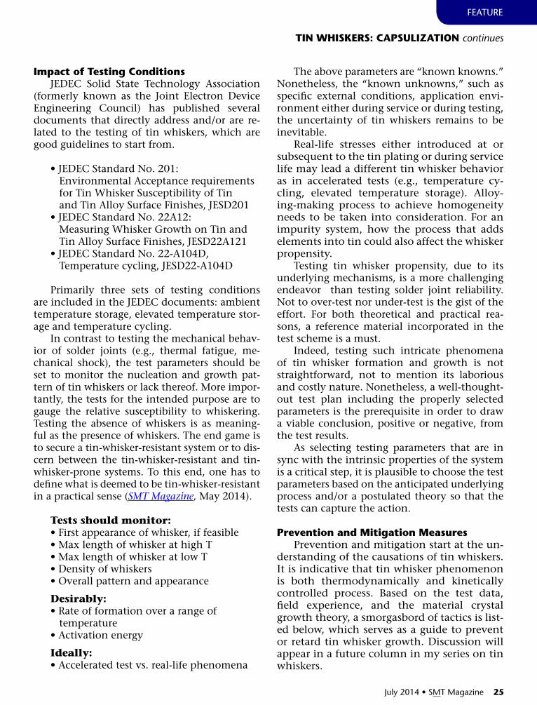
Impact of Testing ConditionsJEDEC Solid State Technology Association
(formerly known as the Joint Electron Device Engineering Council) has published several documents that directly address and/or are re-lated to the testing of tin whiskers, which are good guidelines to start from.
• JEDEC Standard No. 201: Environmental Acceptance requirements for Tin Whisker Susceptibility of Tin and Tin Alloy Surface Finishes, JESD201• JEDEC Standard No. 22A12: Measuring Whisker Growth on Tin and Tin Alloy Surface Finishes, JESD22A121• JEDEC Standard No. 22-A104D, Temperature cycling, JESD22-A104D
Primarily three sets of testing conditions are included in the JEDEC documents: ambient temperature storage, elevated temperature stor-age and temperature cycling.
In contrast to testing the mechanical behav-ior of solder joints (e.g., thermal fatigue, me-chanical shock), the test parameters should be set to monitor the nucleation and growth pat-tern of tin whiskers or lack thereof. More impor-tantly, the tests for the intended purpose are to gauge the relative susceptibility to whiskering. Testing the absence of whiskers is as meaning-ful as the presence of whiskers. The end game is to secure a tin-whisker-resistant system or to dis-cern between the tin-whisker-resistant and tin-whisker-prone systems. To this end, one has to define what is deemed to be tin-whisker-resistant in a practical sense (SMT Magazine, May 2014).
Tests should monitor:• First appearance of whisker, if feasible• Max length of whisker at high T• Max length of whisker at low T• Density of whiskers• Overall pattern and appearance
Desirably:• Rate of formation over a range of temperature• Activation energy
Ideally:• Accelerated test vs. real-life phenomena

26 SMT Magazine • July 2014
• Organic content – <0.05% (a typical military requirement)• Coating grain size – 0.5 to 5 mm – (matte Sn 1 -10 mm)• Coating thickness – < / = 2 mm or > 8 mm• Coating surface morphology – Semi-bright• Coating crystal orientation• Additional process, e.g., – Fusion – Reflow – Annealing (150°C, one hour) • Surface intactness – Absence of surface corrosion – Free of surface notches, scratches, grooves… • Minimize deformation – Avoid external mechanical force imposed on the coating surface• Use of underlying barrier for Cu substrate – Ni layer with nominally 0.5 to 2 micron thickness• Minimize CTE mismatch of the system• Minimize heat excursion• Choice of conformal coating • Change to a composition that is less prone to whiskering when needed• Dipping process• Use of alloying tactics (vs. SnPb)• Most effective elements include Bi, In• SnCu is not a good in whisker-resistance
In order to prevent and retard tin whisker growth, it is highly recommended to exercise the good practice by using aggregate tactics to suppress its driving forces to the level that is be-low the threshold.
Relative Effectiveness—use of Alloy Tactic
My anticipated effectiveness of tin-based materials in preventing and mitigating tin whis-ker formation and growth in descending order is depicted here:
1. SnBi, SnPb2. SnZn 3. SnAg, SAC
4. SnCu 5. Sn
Plausible TheoriesTin whiskers occur by science. What are
the driving forces that initiate the formation of whiskers? What sustain the growth? Can these driving forces be controlled practically and eco-nomically?
These are million dollar questions and de-serve a deliberate treatment. Overall, disparities in theories and reports abundantly exist. Thus far, there is not a uniform conclusion on the theory and mechanism behind tin whisker occurrence.
Discussion of plausible postulation will ap-pear in the future publication of my column se-ries on tin whiskers. Below outlines some key points to be addressed.
Whisker involves an intricate and complex process. Under accelerated test conditions or in real life services, the understanding of tin whis-ker calls for a deeper atomic level treatment con-sidering crystal structure, crystal orientation, grain size, grain boundaries, grain boundaries mobility, atomic mobility, and lattice structural changes to foreign elements. This goes to the heart of physical metallurgy theories in crystal nucleation and grain growth, by normal growth and by abnormal (protruding) growth, from a high energy state to a low energy or to a stress-free state.
Driving to the stress-free state involves sev-eral stages:
• Forming nuclei • Nucleation • Grain and sub-grain growth• Impingement of grains • Classical grain growth
Tin crystal structure (body-centered tetrago-nal, Figure 6) differentiates tin from other met-als that are less prone to whiskering. The aniso-tropic properties of tin result in different surface energies of grains exposed at the surface. This difference and the immobility of grain bound-aries pinned by surface grooves is expected to favor “abnormal” grain growth.
Relatively speaking, the energy to drive grain growth is very low and so it tends to oc-
TIN WHISKERS: CAPSulIzATIoN continues
fEATURE

We deliver AdvancedPCB Solutions!
Landless Via TechnologyWe’re the only manufacturer in the world to haveperfected a liquid photo-imageable resist (PiP) in
electrolytic form, used for all our production.
CLICK TO LEARN MORE
With our panel plating process combined with continuous foil lamination, our impedance tolerances
are second to none!
Impedance Tolerance <5%!
CLICK TO LEARN MORE
Fine line PCB, 2 mil line /spaceWe have developed a unique set of processes based on
electro-depositable liquid photoresist.
CLICK TO LEARN MORE
CANDOR INDUSTRIES, INC.ADVANCED PCB SOLUTIONS
www.candorind.com | [email protected] | (416) 736-6306
Our unique processes enable us to create and deliver Advanced
PCB Solutions that meet the needs of the demanding market
at competitive prices!

28 SMT Magazine • July 2014
TIN WHISKERS: CAPSulIzATIoN continues
cur at much slower rates and is easily changed by the presence of second phase particles or sol-ute atoms in the structure. The external tem-perature (test temperature) drives the kinetics of defect dynamics in the tin layer by affecting stress relaxation and atomic mobility-related mechanisms. For instance, a high temperature (relative to tin’s recrystallization temperature) is expected to impede the continued growth along the protruding direction, resulting in short whiskers. It is also worth noting that tin’s recrystallization temperature changes with the level of its purity. In other words, when add-ing elements into tin, tin’s behavior in relation to the external temperature (test temperatures) will change.
The propensity of a tin deposit to grow whiskers strongly depends on its structure: grain size and the relative crystallographic ori-entation of grains in the deposit. The evidence of recrystallization and grain growth prior to whisker formation is presented for bright tin deposit—large irregular shape grains that are the precursors for whiskers. However, recrys-tallization is only a part of the tin whisker process.
Further key points include:
• If there is sufficient strain to drive nucleation, whisker grain nuclei may form• If there is sufficient “stored” energy, whisker may grow
• To sustain growth, tin material has to be adequately supplied, and tin atoms need to be able to move to a whisker grain through passable paths • Driving forces push the tin from the free surface of the whisker grain outward, resulting in protruding whiskers• The appearance of whiskers in a range of shapes and lengths from rounded mound to long needles depends on relative nuclei sites, stored energy and temperature• But as an aggregate, two points are clear: 1) the driving forces are stress-related, and 2) internal stresses (compressive or tensile) play an important role to both whisker formation and growth • Various tests were performed under temperature cycling and electric field. The lack of harmonious testing results regarding the effects of temperature cycling and electric field on whisker growth suggests the intricate nature of the internal stresses engaged in the process. It is safe to say that tin whiskering is more
than a classical recrystallization process and it is more than a classical stress relief phenomenon. I would say that, for a given tin-based material, there is a threshold strain and there is a thresh-old temperature (in lieu of recrystallization temperature) to cause tin whiskering.
Concluding RemarksOur effort is to alleviate the uncertainty, ul-
timately control tin whiskering propensity.Each of the mitigating tactics has its limi-
tations. Combined tactics offer a high level of confidence in preventing tin whisker-related reliability issues. And each of the causes and factors as discussed does not play out by itself. An illustration is the Ni layer approach that has been proven to be effective in most cases. None-theless, a photo in one NASA report[7] reveals that Ni layer did not categorically prevent tin whisker as shown in Figure 6.
Some of causes and factors as listed above are intricately interplayed and application-spe-cific. This is the challenge imposed to the evalu-ation of tin whisker propensity based on a set of testing conditions. And this is also the very
fEATURE
figure 7: Tin whiskers—tin crystal structure.

July 2014 • SMT Magazine 29
TIN WHISKERS: CAPSulIzATIoN continues
4. BAE Systems/Celestica study.5. S. Meschter, P. Snugovsky, J. Kennedy,
Z.Bagheri#, and E. Kosiba, “SERDP Tin Whis-ker testing and Modeling: High temperature/Humidity Conditions”, ICSR Toronto, Ontario 2013.
6. S. Sakuyama & M.Kutami, “Substitute Ma-terials for Complete Elimination of hazardous Substances – Study of Whisker growth on lead-free Plating”, Fujitsu Sci. Tech. J., 41. 2. (2005).
7. NASA Goddard Space Flight Center report.
upcoming AppearancesDr. Hwang will present a lecture on “Tin
Whiskers – What is Important to Know” at SMT International Conference/Exhibition, on Sep-tember 28 in Chicago, IL.
fEATURE
reason that tin whisker appears to be elusive. Seeking an absolute prevention is hardly a
practical task. Based on the scientific principles as well as the decades’ field service performance, a tin-lead reference material containing lead in the range of 3% to 37% is indispensable. And this defines tin-whisker-resistance.
As to which preventive approach to take, it is the priority setting in the order of importance and effectiveness by assessing the design and specific application. For whisker-sensitive ap-plications, with practical importance in mind, steps to be taken in descending priority steps are: step one is not to use pure tin; step two is to select an effective composition of tin-based al-loy; steps three, four or five, if needed, are to be selected from the above list with the assessment based on the specific system.
There are a number of SAC alloy compo-sitions and the number of the compositions is looming. A specific composition of an SAC should be specified (e.g., SAC105 has different mechanical behavior and physical phenomena from SAC305).
Lead-free solder comprises a wide array of alloy systems not to mention that each alloy system can be modified in numerous ways. The bottom line is that an alloy, SAC or other, does not represent the material world of lead-free un-less a sufficient testing scheme comprising rep-resentative materials is designed and the rep-resentative tests are conducted to validate the “representation.”
In whisker phenomenon, the physical met-allurgy engaged in the process is complex and intricate—a compositional shift and /or an addi-tion of extraneous elements to a base alloy system can change its whisker propensity enormously. Tin whisker propensity under a study should be concluded with a specific alloy composition—the clarity is the name of the game. SMT
References1. (ISBN: 9780901150400) “Environment-
Friendly Electronics—Lead Free Technology”, Electrochemical Publications, LTD, Great Brit-ain, 2001, Page 697.
2. Courtesy of Lucent Technologies.3. Courtesy of George Milad, Uyemura In-
ternational.
Dr. Hwang, a pioneer and long-standing contributor to SMT manufacturing since its inception as well as to lead-free develop-ment and implementation, has helped improve production
yield and solved challenging reliability issues. Among her many awards and honors, she is inducted into the WiT international Hall of fame, elected to the national Academy of Engineering, and named an R&D-Stars-to-Watch. Having held senior executive positions with Lockheed Martin Corp., Sherwin Wil-liams Co., SCM Corp, iEM Corp., she is cur-rently CEo of H-Technologies group provid-ing business, technology and manufacturing solutions. She has served on U.S. Commerce Department’s Export Council, various national panels/committees, and the board of fortune 500 nySE companies and civic and university boards. She is the author of 400+ publications and several textbooks, and an international speaker and author on trade, business, educa-tion, and social issues. Her formal education includes four academic degrees (Ph.D., M.S., M.A., and B.S.) as well as Harvard Business School Executive Program and Columbia Uni-versity Corporate governance Program. To read past columns, click here. for further in-formation, go to: www.jenniehwang.com.
30 SMT Magazine • July 2014
AbstractTin-rich solders are widely applied in the
electronic industry in the majority of mod-ern PCBs. Because the use of lead-tin solders has been banned in the European Union since 2006, the problem of the bridging of adjacent conductors due to tin whisker growth (limited before by the addition of Pb) has been reborn. In this study, tin alloys soldered on glass-epoxy laminate (typically used for PCBs) are consid-ered. Scanning ion microscopy with focused ion beam (FIB) system and energy-dispersive X-ray spectroscopy (EDXS) were used to determine correlations between spatial non-uniformities
of the glass-epoxy laminate, the distribution of intermetallic compounds and whisker growth.
IntroductionTin whiskers are crystals growing from tin or
tin-alloy surface that are a threat to the reliabil-ity of electronic circuits because of short circuits (due to the bridging of adjacent conductors), increased electromagnetic radiation or device littering [1,2]. The phenomenon can occur in tin-rich solders, but the addition of lead to the tin alloy inhibits whisker growth. In the twentieth century, the most popular solder was Pb37Sn63 eutectics. However, since July 2006, when the Restriction of Hazardous Substances (RoHS) Di-rective was adopted by the European Union, the amount of Pb in solders has been limited to 0.1 wt.%. The application of tin-rich lead-free solders in the PCB assembly process has reintro-
Whisker Growth in Tin Alloys
on Glass-epoxy Laminate
fEATURE
by A. Czerwinski, A. Skwarek, M. Płuska, J. Ratajczak, K. Witek inSTiTUTE of ELECTRon TECHnoLogy

32 SMT Magazine • July 2014
duced the problem of tin whisker growth which had been limited before by the addition of Pb. Whiskers are responsible for many system fail-ures in the military, medical and telecommuni-cation industries.
There is no single, commonly accepted mod-el of whisker growth in the literature [2]. How-ever, most theories involve the role of compres-sive stress [2-5], which may result from chemical, mechanical and thermal factors, with the whis-ker growth as a phenomenon of stress relief. The growth is affected by such factors as tem-perature, residual stress, mechanical force, the formation of intermetallic compounds (IMCs), broken oxide layer, electric field, etc. The higher the compressive stress, the greater the volume of Sn contained in whiskers [6].
In typical PCBs with a copper layer above a laminate substrate, the compressive stress gen-erated as a result of volume expansion during the formation of IMCs (a Cu-Sn alloy formed at the Sn/Cu interface), is generally regarded as the driving force for Sn whisker growth. Whisker formation during thermal stress is also induced to a great extent by compressive stress resulting from the thermal expansion coefficient (CTE) mismatch of different layers. It has also been observed that when a tin-alloy layer is deposited on copper and there is compressive stress in-duced by IMCs created at the interface between tin and copper, the compressive stress near the
surface is lower for thicker films, which there-fore are more resistant for tin whisker formation [7,8]. Although full agreement has not yet been reached, it is suggested that when tin plating is over 5 µm [9] (or 8 µm [10]) thick then the layer is more resistant to the whisker growth. Thick-nesses below 0.5 µm and above 20 µm retard growth even more [9], although these very thin or thick plates may not be feasible in practice.
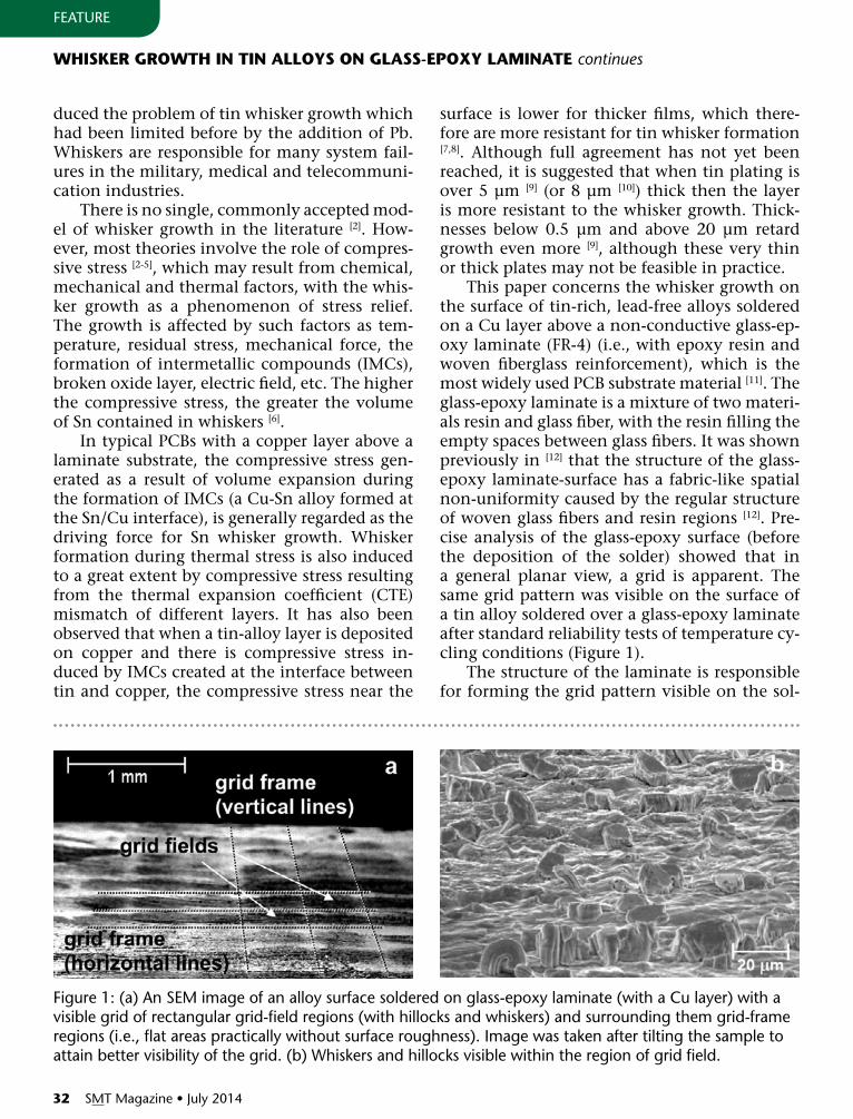
This paper concerns the whisker growth on the surface of tin-rich, lead-free alloys soldered on a Cu layer above a non-conductive glass-ep-oxy laminate (FR-4) (i.e., with epoxy resin and woven fiberglass reinforcement), which is the most widely used PCB substrate material [11]. The glass-epoxy laminate is a mixture of two materi-als resin and glass fiber, with the resin filling the empty spaces between glass fibers. It was shown previously in [12] that the structure of the glass-epoxy laminate-surface has a fabric-like spatial non-uniformity caused by the regular structure of woven glass fibers and resin regions [12]. Pre-cise analysis of the glass-epoxy surface (before the deposition of the solder) showed that in a general planar view, a grid is apparent. The same grid pattern was visible on the surface of a tin alloy soldered over a glass-epoxy laminate after standard reliability tests of temperature cy-cling conditions (Figure 1).
The structure of the laminate is responsible for forming the grid pattern visible on the sol-
WHISKER GRoWTH IN TIN AlloyS oN GlASS-EPoxy lAMINATE continues
fEATURE
figure 1: (a) An SEM image of an alloy surface soldered on glass-epoxy laminate (with a Cu layer) with a visible grid of rectangular grid-field regions (with hillocks and whiskers) and surrounding them grid-frame regions (i.e., flat areas practically without surface roughness). image was taken after tilting the sample to attain better visibility of the grid. (b) Whiskers and hillocks visible within the region of grid field.


34 SMT Magazine • July 2014
WHISKER GRoWTH IN TIN AlloyS oN GlASS-EPoxy lAMINATE continues
fEATURE
der surface. Local compressive stress in the sol-der layer due to large differences in the coef-ficient of thermal expansion (CTE) of the resin and glass fiber promotes whisker growth in the area of the alloy soldered on the Cu layer over the glass fiber (Figure 1) (i.e., in regions of grid fields of the visible grid pattern [12]). The coef-ficient of thermal expansion is much higher for the resin (e.g., about 63 ppm/°C), than for the glass fiber (about 5 ppm/°C) [11], while for tin and copper it is equal to 23 ppm/°C and 16.5 ppm/°C, re-spectively. This effect does not occur for an alloy soldered on Cu over a paper-phenol lami-nate, for example. The lines of the grid frame correspond to the area of the solder placed over the resin while the grid fields between the grid frames correspond to the area of the solder placed over the glass fi-ber in a cross-section [12].
ExperimentThe studied samples were PCB glass-epoxy
laminate covered by a Cu foil (at least 17 µm thick) with a layer of tin or other, commer-cially available tin rich solder alloys: Sn100C (Sn99.3Cu0.7Ni), Sn99Cu1, Sn97Cu3, Sn99.5Ag3Cu0.5, Sn99.3Cu0.7AgNiGe, and Sn99Ag0.3Cu0.7NiGe. The alloys were applied by hand soldering with the application of a water flux. The soldering temper-ature was dependent on the alloy composition.
The samples were tested in a VO¨ TSCH chamber for 1500 shocks within a cyclic tem-perature range of -45°C to +85°C, with each cycle lasting 20 min and the transition time of the lift between hot and cold zones equal to 5 s. These conditions are recommended by iNEMI (International Electronics Manufactur-ing Initiative) and JEDEC (Joint Electronic De-vice Engineering Council) as inducing whisker growth in most Sn and Sn-alloy layers [13].
The FEI Helios NanoLab 600 DualBeam FIB system was applied to the milling (cross-section-ing) of samples with a precise gallium ion beam and also for scanning ion microscopy imaging (i.e., induced by the ion beam and detected by
the secondary-electron detector) for the range of energies up to 30 keV. The cross-sections were thoroughly cleaned in FIB to remove contami-nations introduced during the FIB cross-sec-tioning process [14, 15]. EDXS with a Philips XL30 SEM and EDAX spectrometer (with 130 eV spec-tral resolution) was used, with an energy range
from 5–15 keV applied in the consid-ered case.
Results and DiscussionScanning ion microscopy
imaging and EDXS measure-ments were performed at vari-ous points on the mentioned grid to determine the correla-tions between the spatial non-uniformities of the structure of glass-epoxy laminate, of IMC distribution in the solder and of whisker growth after standard reliability tests. The grid on the solder is formed by
grid fields (rectangular regions with hillocks and whiskers) sur-
rounded by the grid frame (flat re-gions without surface roughness).
The measurements were first performed when the samples were observed in a planar view, with the sample surface placed perpen-dicular to the electron beam. Results obtained from grid fields (with hillocks and whiskers) showed a significant Cu content, much higher than that from grid frames where this content was negligible.
Afterwards, FIB was used for milling sam-ples with a gallium ion beam. These cross-sec-tions were performed at several adjacent points spaced along a line from the grid frame to the grid field, with the aim of comparing neighbor-ing points (instead of comparing random points in these two regions, because additional factors may be relevant in remote locations).
Images of cross-sectioned layers were taken by use of electron and ion microscopy. The scan-ning ion microscopy performed in FIB system, where detected secondary electrons are generat-ed by the incident gallium ions, allowed for bet-ter image contrast than that observed in images obtained from standard secondary-electron (SE)
The lines of the grid frame correspond to the area of the solder placed over the resin while the grid fields between the grid frames correspond to the area of the solder
placed over the glass fiber in a cross-section.
“
”

July 2014 • SMT Magazine 35
or backscattered-electron (BSE) modes of SEM. Various tin-alloy, copper and IMC grains look quite different in these FIB images (Figures 2, 3), due to significantly different ion channeling in-side various grains even in the case of the same material (e.g., tin alloy [16]).
Small dotted lines drawn along boundaries of IMC layer (at the alloy/Cu interface) enhance its visibility in the Figure 2a. Due to tilting of the sample the vertical marker is different from the horizontal one.
Cross-section images show three metal-lic layers above the laminate: a Cu layer at the bottom, a tin-alloy layer on the top and a thin IMC layer between them. The studies revealed a distinct difference between distinguished re-gions of grid frames and grid fields with respect to the quantity, size and location of IMC pre-cipitates within the solder layer (Figures 2 and 3). Although in the region of grid frames even long Cu6Sn5 protrusions extended into the sol-der layer from the IMC layer (i.e., situated at the interface between the layers of tin-alloy and copper), but only small IMC precipitates (with a sub-micrometer diameter) were observable in-side the solder layer(i.e., without a direct con-tact with the IMC layer), as shown in Figures 2a,b.
figure 2: Scanning ion microscopy image of cross-sections milled by fiB in three consecutive adjacent places along a line from the grid-frame to the grid-field region: (a, b) in the grid-frame region; (c) at the boundary between the grid-frame and the grid-field regions. from the bottom to top, the copper film, the interface iMC layer (with iMC protrusions extending upwards) and the solder layer (with small separate Cu6Sn5 precipitates inside) becoming thicker towards the grid-field region, are visible in these cross-sections.
figure 3: Scanning ion microscopy image of cross-sections milled by fiB in the grid field re-gion in the two consecutive adjacent places along a line from the grid-frame to the grid-field region (situated next to the three places shown in figure 2). going from the bottom to the top the copper film, the interface iMC layer and the solder layer (with large separate Cu6Sn5 precipitates inside) are visible in these cross-sections. Due to tilting of the sample the vertical marker is different from the horizontal one.
WHISKER GRoWTH IN TIN AlloyS oN GlASS-EPoxy lAMINATE continues
fEATURE

36 SMT Magazine • July 2014
In contrast, in the region of grid fields much bigger IMC precipitates (with diameters even in the range 5-8 µm) were observed inside the sol-der layer, without a direct contact with the IMC layer and close to the solder top surface (Figures 3a,b). In many cases densely distributed round-shaped Cu6Sn5 precipitates with diameters from one to several micrometers even reached the top surface of the tin alloy and these were ob-servable at close distances from each other (Fig-ure 4). The occurrence of IMC precipitates on solder surfaces has been observed previously [17].
Numerous previous observations have shown and discussed IMC protrusions extend-ing from the IMC layer into the solder layer as well as have shown IMC precipitates located within the solder layer and positioned along grain boundaries [18, 19]. However, in our inves-tigations (as well as observations in some other studies [20]) Cu6Sn5 precipitates were found not
only along grain boundaries but also inside the solder grains, i.e., without a visible contact with grain boundaries (Figures 2, 3 and 5). Separate Cu6Sn5 precipitates were also observed even in-side some whisker crystals (Figure 5), confirm-ing that during their upward migration IMCs can penetrate into various grains. It can also be seen in this figure that the density of IMC precipitates in the solder increases closer to the whisker.
Generally, during the soldering operation, material from the metal sublayer dissolves and mixes with the solder, allowing the formation of IMCs. In alloys consisting of Sn and Cu, two different phases of IMCs may be present: Cu6Sn5 and Cu3Sn. Especially the formation of a Cu6Sn5 phase (because of its large-volume expansion in comparison with the pure tin) is a strong fac-tor promoting whisker growth in the neighbor-ing alloy [3]. Our EDXS measurements revealed a content of about 39 wt.% Cu in the IMC layer at the interface between copper and tin-alloy layers, i.e. measurably equal to the Cu content in the Cu6Sn5 layer. The same content of about 39 wt.% Cu was found for all measured IMC precipitates observed within the tin-alloy layer, confirming that they also constituted a Cu6Sn5 phase. In contrast, the content of Cu in another possible Cu-Sn IMC phase (i.e., Cu3Sn) would
fEATURE
figure 4: SEM image of a single whisker. Densely distributed round-shaped Cu6Sn5 precipitates at the top surface of the tin alloy at the grid field are visible close to the whisker apparent in the center of the image. EDXS spectrum (obtained at elec-tron energy 15 kev) of an example precipitate is shown below.
figure 5: Scanning ion microscopy image of a cross-section with a whisker grown in the grid-frame region. An increased density of Cu6Sn5 pre-cipitates in the tin-alloy solder close to the whis-ker base and a small separate Cu6Sn5 precipitate inside the whisker are seen.
WHISKER GRoWTH IN TIN AlloyS oN GlASS-EPoxy lAMINATE continues


38 SMT Magazine • July 2014
be equal to above 60 wt.% Cu, much higher than revealed in our measurements.
In contrast, no distinguishable difference in the shape of the interface IMC layer was observed between the two regions (of the grid frame and of grid fields, see Figures 2 and 3). This means that the spatial non-uniformity caused by the regular structure of glass fi-bers and resin regions in the top layer of a glass-epoxy laminate also promotes spatial non-uni-formity of the IMC-precipitate distribution within the solder layer, often close to its top sur-face. This effect seems to con-stitute an additional factor for the apparent non-uniformity of whisker growth.
Thick solder layers (signifi-cantly more than 10 µm) were applied in samples to ensure their resistance to whisker growth. Cross-sections performed in regions adjacent to grid frames and grid fields show that the thickness of tin alloy in the frame regions is significantly lower than in the field regions, e.g., equals about 13 µm at the grid frame (Figure 2a) while about 18 µm in the adjacent regions of grid fields (Figures 3a,b). The calculation of alloy thickness takes into ac-count that the studied samples were tilted during observations in the microscope chamber. Thus markers shown in Figures 2, 3 and 5 represent horizontal dimensions, while the vertical dimen-sions are underestimated and therefore their mul-tiplication by the tilt angle secant is required (i.e., by 1.24, because the tilt angle equals 36° there).
Whisker growth depends on many factors with an impact of one factor being distinguish-able only when other important factors are fixed. Although a thinner (if not very thin) solder is considered to be more prone to whisker growth [7-10], the mentioned additional factors related to the compressive stress have forced an absence of whiskers in grid frame regions (with thinner sol-der), and their presence in regions of grid fields (with thicker solder).
Much higher thermal expansion coefficient of the resin than of the glass fiber causes the resin to expand and shrink more than the glass fiber during tests performed with a cyclic temperature
range of -45°C to +85°C. A nonuniform expansion of the top area of the glass-epoxy laminate occurs in its longisection, as well as in its cross-section. It may be expected that alongside differences in compressive stress in adjacent regions, the lay-ers in various regions will be differently affected
mechanically, shifted and pushed up during temperature cycles.
The observed non-uniform spatial distribution of IMC pre-cipitates seems to occur due to differences in mechanical interactions and compressive stress in various regions, while the presence of IMCs is a driv-ing force for whisker growth. Therefore, it may be expected that CTE differences in various regions of PCBs with tin-alloy
on glass-epoxy laminate facili-tate spatially non-uniform whisker
growth in two ways, directly by the implemented compressive stress and indirectly by the generation of non-uniform IMC distribution.
SummaryWhisker growth on the surface of tin alloys
soldered above a glass-epoxy laminate was stud-ied (i.e., for the most widely used PCB substrate material). The structure of the glass-epoxy lami-nate surface has a spatial non-uniformity caused by the regular structure of glass fibers and resin regions in the top layer of the laminate. There-fore, the local compressive stress in the solder layer due to differences in the thermal expan-sion of the resin and glass fiber promotes whis-ker growth in the area of the alloy soldered on the Cu layer over the glass fiber.
Scanning ion microscopy using the FIB sys-tem and EDXS performed after standard reliabil-ity tests determined a strong correlation between the structure of glass-epoxy laminate, the spatial distribution of IMCs and whisker growth. In the region of grid frames only small IMC precipitates were observable inside the solder layer (i.e., with-out a direct contact with the IMC layer situated at the interface between the tin-alloy and Cu lay-ers). In contrast, in the region of grid fields much bigger IMC precipitates were observed inside the solder layer, without a contact with the IMC layer
WHISKER GRoWTH IN TIN AlloyS oN GlASS-EPoxy lAMINATE continues
fEATURE
Whisker growth depends on many
factors with an impact of one factor being distinguishable only
when other important factors are fixed.
“
”

July 2014 • SMT Magazine 39
whisker growth in tin alloys on glass-epoxy laminate continues
FeaTure
and close to the solder top surface. Densely dis-tributed round-shaped Cu6Sn5 precipitates with diameters from one to several micrometers also reached the top surface of solder in many places.
It can be concluded that CTE differences of various PCB regions with tin alloys on glass-epoxy laminate facilitate spatially non-uniform whisker growth directly by the non-uniform compressive stress and indirectly by the generation of a non-uniform spatial distribution of IMCs. smt
acknowledgementsThe work has been partially supported by
the National Science Centre (project number N N515 503940).
references1. D. Pinsky, M. Osterman, S. Ganesan, IEEE
Transactions on Components and Packaging Tech-nologies 27, 427 (2004).
2. G.T. Galyon, IEEE Transactions on Electronics Packaging Manufacturing 28, 94 (2005).
3. G.T. Galyon, L. Palmer, IEEE Transactions on Electronics Packaging Manufacturing 28, 17 (2005).
4. C. Xu, Y. Zhang, C. Fan, J.A. Abys, IEEE Trans-actions on Electronics Packaging Manufacturing 28, 31 (2005).
5. J. Smetana, IEEE Transactions on Electronics Packaging Manufacturing 30, 11 (2007).
6. J. Cheng, S. Chen, P.T. Vianco, J.C.M. Li, Jour-nal of Applied Physics 107, 074902 (2010).
7. B.D. Dunn, A laboratory study of tin whisker growth, European Space Agency (1987).
8. J. Cheng, F. Yang, P.T. Vianco, B. Zhang, J.C.M. Li, Journal of Electronic Materials 40, 2069 (2011).
9. X.C. Tong, Advanced Materials for Thermal Management of Electronic Packaging (Springer Series in Advanced Microelectronics) Schaumburg 2011.
10. R. Schetty, Circuit World 27, 17 (2001).11. R. Sanapala, Characterization of FR-4 Printed
Circuit Board Laminates Before and After Exposure to Lead-free Soldering Conditions, ProQuest LLC, Ann Arbor, 2008.
12. A. Skwarek, M. Pluska, A. Czerwinsky, K. Wi-tek, Materials Science and Engineering B177, 1286 (2012).
13. N. Vo, M. Kwoka, P. Bush, IEEE Transac-tions on Electronics Packaging Manufacturing 28, 3 (2005).
14. J. Orloff, M. Utlaut, L. Swanson, High Reso-lution Focused Ion Beam: FIB and Its Applications,
Kluwer Academic/Plenum Press, New York 2003.15. L.A. Giannuzzi, F.A. Stevie, Introduction to
Focused Ion Beams: Instrumentation, Theory, Tech-niques and Practice, Springer, New York 2005.
16. S.W. Liang, C. Chen, J.K. Han, L. Xu, K.N. Tu, Y.-S. Lai, Journal of Applied Physics 107, 093715 (2010).
17. S. Choi, K.N. Subramanian, J.P. Lucas, T.R. Bieler, T.R., Journal of Electronic Materials 29, 1249 (2000).
18. G.T.T. Sheng, C.F. Hu, W.J. Choi, K.N. Tu, Y.Y. Bong, L. Nguyen, Journal of Applied Physics 92, 64 (2002).
19. K.N. Tu, J.C.M. Li, Materials Science and En-gineering A 409, 131 (2005).
20. C.-F. Yu, C.-M. Chan, K.-C. Hsieh, Microelec-tronics Reliability 50, 1146 (2010).
This article originally appeared in the Archives of Metallurgy and Materials, vol. 58 (2) s. 413-417 (2013).
Andrzej Czerwinski (PhD, DSc) is associate professor and head of Department of Materials and Semiconductor Structures Research, Institute of Electron
Technology, Warsaw, Poland.
Agata Skwarek (PhD) is an assis-tant professor in the Department of Microelectronics in the Institute of Electron Technology (Krakow Division), Poland.
Mariusz Pluska (PhD) and Jacek Ratajczak (PhD) are assistant professors with the Department of
Materials and Semiconductor Structures Research, Institute of Electron Technology, Warsaw, Poland.
Krzysztof Witek (M.Sc. Eng.) works in the Institute of Electron Tech-nology (Krakow Division), Poland as manager of Implementation and Production Department.

40 SMT Magazine • July 2014
Abstract The objective of this study is to evaluate
conformal coatings for mitigation of tin whis-ker growth. The conformal coatings chosen for the experiment are acrylic, polyurethane and parylene. The coatings were applied in thick-nesses ranging from 0.5 to 3.0 mils on 198 bright tin plated coupons with a base metal of either Copper C110 or Alloy 42. Prior to coat-ing, light scratches were applied to a portion of the coupons, and a second fraction of the coupons were bent at 45° angles to provide sources of stress thought to be a possible ini-tiating factor in tin whisker growth. The cou-pons have been subjected to an environment of 50°C with 50% relative humidity for 9.5 years. Throughout the trial period, the samples were inspected by both optical and scanning elec-tron microscopy for tin whisker formation and penetration out of the coatings by tin whiskers. Tin whiskers were observed on each coupon in-
cluded in the test, with stressed regions of the bent samples demonstrating significantly high-er tin whisker densities. In addition, the Alloy 42 base metal samples showed greater tin whis-ker densities than the Copper C110 base metal samples. There were no observable instances of tin whisker penetration out of the coatings or tenting of the conformal coat materials for any of the non-stressed test coupons. The stressed coupons demonstrated tin whisker protrusion of the 1.0 and 2.0 mil thick acrylic coating and the 1.0 mil polyurethane coating for the Alloy 42 base metal samples. The greater thickness coatings did not demonstrate tenting or tin whisker protrusion. Also included in this paper are tin whisker inspection results of tin-plated braiding and wire that was exposed to an en-vironment of 50°C with 50% relative humidity for over five years.
Introduction A tin whisker is a spontaneous growth of a
tin crystal from tin-finished surfaces. The crys-tal often grows in a needle-like form, and due to the electrical conductivity of the anomaly,
fEATURE
by linda Woody and William Fox LoCKHEED MARTin MiSSiLES AnD fiRE ConTRoL
Tin Whisker Risk Management by Conformal Coating


42 SMT Magazine • July 2014
fEATURE
there is a resulting risk of current leakage and shorting due to bridging of adjacent conduc-tors. There have been multiple studies into the mechanisms for whisker growth and both en-vironmental and mechanical factors that may promote whisker growth[1-5].
Similarly there have been multiple stud-ies on methods for mitigating tin whisker growth[6,7]. Mathew et al. reviewed research into mitigation strategies such as conformal coating, electroplating techniques, surface treatments, alloying tin, use of various under-plates and an-nealing of tin[6].
The conformal coating miti-gation strategy has shown multiple results using various coating materials and envi-ronmental storage conditions. NASA studies[8-10] indicated that bright tin plated brass coupons, conformal coated with a uralane-based material, was able to prevent tin whis-ker protrusion following nine years of ambient storage when the coating thickness was at least 2.0 mils. If the coating was thinner, there were obser-vations of tin whisker protru-sions.
Woodrow and Ledbury re-leased two papers[11,12] examining tin whisker growth through mul-tiple conformal coating materials. Both studies used bright tin plated brass test coupons. For the first study, when the test coupons were sub-jected to an environmental chamber set to 50°C with 50% relative humidity (RH), tin whisker penetration was noted after approximately one year for coatings of 1.5 mils and less, but not for coatings of at least 3.9 mils. For the second study, the conformal coatings examined were urethane-acrylic hybrid, silicone, acrylic and parylene. The test coupons were subjected to an environmental chamber set to 25°C with 97% RH. All of the test coupons exhibited tin whis-ker penetration of the conformal coatings, even on samples with up to 6.0 mils of coating.
The University of Maryland’s Center for Advanced Life Cycle Engineering (CALCE) has
studied the interfacial strength of conformal coatings in comparison to the whisker buck-ling force[13] initially presented by Kadesch and Leidecker[8]. Preliminary testing indicated that conformal coatings of 25 microns (approximate-ly 1.0 mil) or less with a modulus of 100MPa or less are at risk of tin whisker penetration. Nak-agawa et al. similarly identified harder coatings with high adhesion strengths as the most likely materials to prevent tin whisker protrusion[14].
Han et al. review the effectiveness of confor-mal coatings as a tin whisker mitigator on ac-
tual circuit cards and determined that coating coverage is an essential
factor[15]. As the coating thinned along the edges of component leads, the potential for tin whiskers to protrude through the coating, regardless of the coating type increased dramat-ically. This was confirmed by the NPL’s Hunt and Wickham who designed a test vehicle to determine the propensity of whiskers to grow through coatings and contact a neigh-boring plate[16].
Reviewing the multiple studies on the use of confor-mal coatings as a mitigation
technique for tin whiskers indi-cates that tin whiskers can grow
through a coating. One of the lead-ing factors for the risk of a protrusion through a coating is the thickness. Coating thicknesses below 2.0 mils appear to present a greater risk of tin whisker penetration, although extreme en-vironmental conditions coupled with the type of tin plating could promote tin whisker growth through any type of coating at relatively large coating thicknesses.
This company conformal coats 99% of all circuit boards using one of three different con-formal coating materials: acrylic, polyurethane and parylene. This study examined the effects of tin whisker growth on the three coatings ap-plied to test coupons at varying thicknesses.
Acrylic conformal coatings are perhaps the most popular of all conformal coating materi-als due to their ease of application, removal and
TIN WHISKER RISK MANAGEMENT By CoNFoRMAl CoATING continues
Reviewing the multiple studies on the use of
conformal coatings as a mitigation technique
for tin whiskers indicates that tin whiskers can
grow through a coating. One of the leading
factors for the risk of a protrusion through a coating is the thickness.
“
”

July 2014 • SMT Magazine 43
forgiving nature[17]. Acrylics dry rapidly, reach-ing optimum physical properties in minutes, are fungus resistant and provide long pot life. Additionally, acrylics give off little or no heat during cure eliminating potential damage to heat-sensitive components. They do not shrink during cure and have good humidity resistance and exhibit low glass transition temperatures.
Polyurethane coatings are available as either single or two-component formulations[14]. Both formulations provide excellent humidity resis-tance and far greater chemical resistance than acrylic coatings. Single component polyure-thanes, while easy to apply, enjoy long pot life but sometimes require very lengthy cure cycles to achieve full or optimum cure. Two compo-nent formulations can reach optimum cure properties in as little as one to three hours with the assistance of heat. However, when compared to single component formulations, two-compo-nent formulas can have a relatively short pot life sometimes making them difficult to work with. Since polyurethanes are polymerized and cross-linked in place, they have excellent resistance to chemicals, moisture and solvents. They are available in tough, abrasion-resistant varieties and also in low modulus varieties for extreme temperature ranges. Polyurethanes have good adhesion to most materials and provide for a robust coating process. The material is difficult to remove following cure except by thermal or mechanical means.
The parylene coating is chemically inert and moisture resistant[14]. Very thin, uniform layers can be applied to the surface with no pinholes or voids. Parylene coating has a high dielectric strength. Due to the nature of the deposition process used to apply the coating, there are no volatiles generated. Parlylene coatings are ex-tremely low weight and yet have the highest modulus of the three coatings being examined. The coating process must be performed in batch mode, using specialized coating equipment. Re-work is difficult, and a microabrasion process is usually required to remove the coating.
The spray process used at the company for application of the acrylic and polyurethane coatings is automated with a rotating spray head. The motion of the head is designed to cover a given width from all angles. Masking is
required to keep coating out of areas that should not be coated.
Parylene is applied at room temperature with deposition equipment that controls the coating rate and ultimate thickness. Polymer deposition takes place at the molecular level in three stages. The raw material dimer is vapor-ized under vacuum and heated to a dimeric gas. The gas is then pyrolized to cleave the dimer to its monomeric form. In the room temperature deposition chamber, the monomer gas deposits as a transparent polymer film.
In addition to tin whisker growth on com-ponent leads and coatings, the risk of tin whis-ker growth on braiding and wires is also of con-cern. Hillman et al. indicated a low risk for tin coated copper wire, braid and cable following exposure of samples to 85°C and 85% relative humidity[18].
Scope and objective This study was designed to examine the ef-
fects of tin whisker growth on the three coat-ings, applied to test coupons at varying thick-nesses. In addition, the tin whisker growth on braiding, stranded wire and solid single strand wire with pure tin coating was also monitored to determine the risk of use in high-reliability products.
Examination of Conformal Coating as a Mitigating Material for Tin Whisker Growth
Test coupons consisting of two types of base material (Copper C110 alloy and Alloy 42) were electrodeposited with a layer of “bright tin” plating. Copper C110 and Alloy 42 are com-mon base metals utilized for component leads. After plating and prior to conformal coating a quantity of the plated coupons were scratched to simulate those found during handling and shipping conditions, and another quantity of plated coupons were bent (without scratches) to induce tensile and compressive stresses on the plating. All of the test coupons were then conformal coated on approximately half of the surface with the other half remaining un-coated. The coupons were masked, coated, and then demasked to ensure the coating thickness was uniform and there was no thinning at the
TIN WHISKER RISK MANAGEMENT By CoNFoRMAl CoATING continues
fEATURE
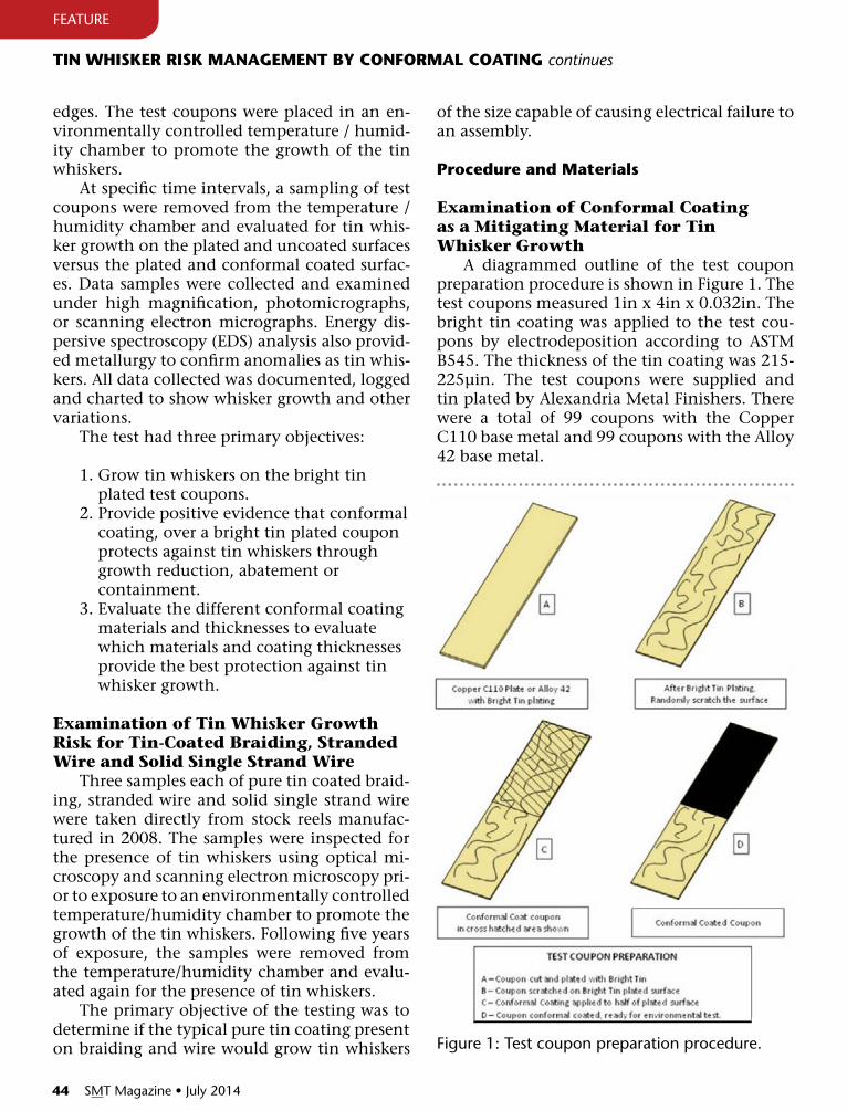
44 SMT Magazine • July 2014
edges. The test coupons were placed in an en-vironmentally controlled temperature / humid-ity chamber to promote the growth of the tin whiskers.
At specific time intervals, a sampling of test coupons were removed from the temperature / humidity chamber and evaluated for tin whis-ker growth on the plated and uncoated surfaces versus the plated and conformal coated surfac-es. Data samples were collected and examined under high magnification, photomicrographs, or scanning electron micrographs. Energy dis-persive spectroscopy (EDS) analysis also provid-ed metallurgy to confirm anomalies as tin whis-kers. All data collected was documented, logged and charted to show whisker growth and other variations.
The test had three primary objectives:
1. Grow tin whiskers on the bright tin plated test coupons. 2. Provide positive evidence that conformal coating, over a bright tin plated coupon protects against tin whiskers through growth reduction, abatement or containment. 3. Evaluate the different conformal coating materials and thicknesses to evaluate which materials and coating thicknesses provide the best protection against tin whisker growth.
Examination of Tin Whisker Growth Risk for Tin-Coated Braiding, Stranded Wire and Solid Single Strand Wire
Three samples each of pure tin coated braid-ing, stranded wire and solid single strand wire were taken directly from stock reels manufac-tured in 2008. The samples were inspected for the presence of tin whiskers using optical mi-croscopy and scanning electron microscopy pri-or to exposure to an environmentally controlled temperature/humidity chamber to promote the growth of the tin whiskers. Following five years of exposure, the samples were removed from the temperature/humidity chamber and evalu-ated again for the presence of tin whiskers.
The primary objective of the testing was to determine if the typical pure tin coating present on braiding and wire would grow tin whiskers
of the size capable of causing electrical failure to an assembly.
Procedure and Materials
Examination of Conformal Coating as a Mitigating Material for Tin Whisker Growth
A diagrammed outline of the test coupon preparation procedure is shown in Figure 1. The test coupons measured 1in x 4in x 0.032in. The bright tin coating was applied to the test cou-pons by electrodeposition according to ASTM B545. The thickness of the tin coating was 215-225µin. The test coupons were supplied and tin plated by Alexandria Metal Finishers. There were a total of 99 coupons with the Copper C110 base metal and 99 coupons with the Alloy 42 base metal.
fEATURE
TIN WHISKER RISK MANAGEMENT By CoNFoRMAl CoATING continues
figure 1: Test coupon preparation procedure.

Miraco, Inc. • 102 Maple Street, Manchester, NH 03103 • miracoinc.com603-665-9449 • Fax: 603-665-9459
...connecting technology
M IRACO
Engineering And Providing Balanced Interconnect Solutions
Our products and services are specifically designed to empower our customers toproduce a product with superior performance and quality, as well as lower design,
assembly, and system installation costs.
Partnering With Your Engineering Team To Deliver The Best Solution
Flexible Printed Circuits • Rigid Flex • Wire Harnesses • Complete Assemblies
MiracoFullPageAd.indd 1 4/3/14 5:23 PM

46 SMT Magazine • July 2014
Following the plating process, 69 Copper C110 base metal coupons and 69 Alloy 42 base metal coupons were scratched along the surface. Brown paper wrapping material was cut in sheet sizes approximately 8.5in x 11in, wrinkled by “balling and crushing” and then unraveled and flattened. Each coupon was separately wrapped (one sheet/coupon), then individually laid on a hard surface (i.e., tabletop) and shuffled around several times on each of the flat sides thereby randomly creating light scratches on the tin surface. These scratches were intended to simu-late those found on the surface of component leads as a result of shipping and handling. The typical light scratch created by this method was photo documented.
fEATURE
TIN WHISKER RISK MANAGEMENT By CoNFoRMAl CoATING continues
Also following the plating process, 30 cop-per C110 base metal coupons and 30 Alloy 42 base metal coupons had a 45° bend placed in 2 places as shown in Figure 2 using a machine vise with appropriate protection applied to the jaws of the vise (i.e., Teflon tape or equivalent). This bend was intended to put the tin plating under stress. Necessary precautions were taken to protect the transfer of metal to the tin plat-ing during the bending process. These coupons do not have scratches in the tin plated surfaces.
The conformal coatings used in the test-ing were acrylic per MIL-C-46058, Type AR, polyurethane per MIL-C-46058, Type UR, and parylene per MIL-C-46058, type XY. Table 1 in-cludes mechanical properties of the coatings
figure 2: Drawing of bent test coupons. (note: for the bent test coupons, the regions of compression and tension in the tin plating, caused through relaxation of the material following the bending process are identified in the schematic.)

July 2014 • SMT Magazine 47
used in the testing. The application thickness of the coatings was 1.0, 2.0 or 3.0 mils for the acrylic and polyurethane coating and 0.5 mils for the parylene coating.
Prior to the coating process, the samples were cleaned using the existing in-line cleaner and then baked at 85°C for two hours. The ap-propriate areas of the coupons were masked using tape. The acrylic and polyurethane coatings were applied using a spray coat process and the parylene coating was applied using a vapor deposition process. All test coupons were coated by the com-pany. The samples were labeled ac-cording to Table 2.
Following the conformal coating of the test coupons, and a visual in-spection to insure continuity of the coating as well as a measurement of the coating thickness on approxi-mately ten samples to insure that the proper coating thicknesses were applied, the samples were placed in an environmental chamber. The en-vironmental chamber was capable of maintaining a temperature of 50° ± 10°C and a relative humidity of 50% ± 15%. The oven was equipped with a fail-safe device to ensure against overheating. The internal working envelope of the environ-mental chamber was 16in x 16in x
Table 1: Properties of confomal coatings used in testing. (note: Properties from material technical data sheets.)
Table 2: Test coupon matrix.
TIN WHISKER RISK MANAGEMENT By CoNFoRMAl CoATING continues
fEATURE

48 SMT Magazine • July 2014
12in. The temperature and humidity was con-tinually monitored by an electronic recording device. The date of the initial insertion of the coupons into the environmental chamber was June 15, 2004.
On one occasion during the last quarter of each year, a sample of test coupons was removed from the environmental chamber and inspect-ed. The inspection consisted first of optical mi-croscopy, using the indirect light procedures de-scribed on the ‘NASA Tin Whisker Homepage’ website [19]. Anomalies in the integrity of the conformal coating were noted, and any areas with suspect tin whisker growth were noted and inspected further using scanning electron mi-croscopy. SEM was also used on the areas of the test coupons without conformal coating to de-termine the length and density of tin whiskers.
Examination of Tin Whisker Growth Risk for Tin-Coated Braiding, Stranded Wire and Solid Single Strand Wire
Three samples each of braiding, stranded wire and solid single strand wire were removed directly from stock reels. The braiding select-ed had a braid length of 4in, an average braid width of 0.172in, an average braid height of 0.029in and a strand quantity of 30. The strand-ed wire selected conformed to the M22759/34-24-9 specification. The insulation was stripped on each sample to expose approximately 3in of wire. The solid single strand wire selected con-formed to the A-A-59551, Type S, 20AWG tin-
coated specification. All of the samples exam-ined were manufactured in 2008.
Prior to environmental exposure, the sam-ples were inspected by optical microscopy and scanning electron microscopy for the presence of tin whiskers. The samples were placed in an environmental chamber set to 50° ± 10°C and a relative humidity of 50% ± 15% in Septem-ber 2008. In September 2013, all of the samples were removed from the environmental cham-ber and again inspected by optical microscopy and scanning electron microscopy for the pres-ence of tin whiskers.
Results and Discussion
Examination of Conformal Coating as a Mitigating Material for Tin Whisker Growth
A detailed review of the annual inspection results for the initial 5.5 years of environmental exposure was reported previously[20].
Original inspection of the test coupons fol-lowing application of the tin plating indicated no observable anomalies in plating integrity (Figure 3). Cross-sections of ten samples con-firmed the plating thickness to be between 215 and 225µin. The thickness of the applied con-formal coating was confirmed from several pre-vious processing tests run to evaluate process-ing parameters for required coating thickness. Inspection of the conformal coating integrity indicated no significant anomalies. The coat-
fEATURE
TIN WHISKER RISK MANAGEMENT By CoNFoRMAl CoATING continues
figure 3: Scanning electron micrographs (800X magnification) demonstrating the condition of the sur-face of the tin plating prior to conformal coating for both the Copper C110 base metal (left) and Alloy 42 base metal (right).
July 2011 • SMT Magazine 47

50 SMT Magazine • July 2014
ing thickness at the line of demarcation for the flat samples tended to be slightly less than that for the remainder of the sample but not signifi-cantly.
Figure 4 includes scanning electron micro-graphs of the tin plating on a Copper C110 base metal coupon at the location of the bend pri-or to conformal coating. There are observable stress cracks in the tin plating caused by the bending process. The tin plating on the Alloy 42 base metal appeared similar.
Inspection Results for Coupons without Conformal Coating
Table 3 includes whisker density values for the uncoated samples for both the Copper C110 base metal and the Alloy 42 base metal on the
control samples and on the bent samples for both regions in tension and compression. As of the fourth quarter of 2013 sampling, the whis-ker density on the Alloy 42 base metal control sample (62 whiskers/mm2) was greater than that of the whisker density on the Copper C110 base metal control sample (39 whiskers/mm2). The largest tin whiskers and odd-shaped eruptions observable on the control samples approached 5.0 mils, indicating that whiskers were present with minimum lengths dimensionally capable of extending through the conformal coating thicknesses applied to the test coupons. The ef-fect of the light scratches applied to the surface of the control samples was negligible with no observable pattern of whiskers accumulating along the scratches.
fEATURE
TIN WHISKER RISK MANAGEMENT By CoNFoRMAl CoATING continues
figure 4: Scanning electron micrographs of the tin plating following the bending process on the Copper C110 base metal.
Table 3: Average tin whisker densities on uncoated regions throughout environmental exposure.


52 SMT Magazine • July 2014
metal coupons (128 whiskers/mm2 in regions of compression and 59 whiskers/mm2 in regions of tension). The length of tin whiskers growing along the surface of the samples from both base metals approached 8.0 mils (Figure 6).
The observations of the conformal coated test coupons as of the fourth quarter of 2013 are summarized in Table 4.
Inspection Results for Straight, Scratched Coupons with Conformal Coating
There were no observed tin whisker protru-sions through any of the conformal coating
As of the fourth quarter 2013 sampling, the whisker densities in the stressed regions were considerably higher than that for the control samples (Figure 5). The regions in compression exhibited greater whisker densities than the regions in tension for both the Copper C110 and Alloy 42 base metal coupons. The whis-kers tended to grow along stress cracks in the tin plating caused by the bending process. The Alloy 42 coupons had significantly greater tin whisker density in both regions of compression (367 whiskers/mm2) and tension (213 whiskers/mm2) than that of the bent Copper C110 base
fEATURE
TIN WHISKER RISK MANAGEMENT By CoNFoRMAl CoATING continues
figure 5: Scanning electron micrographs (100X magnification) demonstrating the density of tin whis-kers on the uncoated areas in the compression regions the bent coupons (top two micrographs) and the regions of tension for the bent coupons (bottom two micrographs).

July 2014 • SMT Magazine 53
TIN WHISKER RISK MANAGEMENT By CoNFoRMAl CoATING continues
fEATURE
materials used on the coupons that were not bent for both base metals (Table 4). In addition, there was no indication of tenting of the con-formal coat where a tin whisker may push the coating away from the tin plating. There were tin whiskers or odd-shaped eruptions observed beneath the conformal coating for samples of both base metals and all coating types; howev-er the observed tin whiskers did not cause any disturbance to the conformal coating. The pres-ence of conformal coating over the tin whis-kers was confirmed by EDS. Figure 7 includes a scanning electron micrograph detailing the interface of the parylene coating to the uncoat-ed region of one coupon. Tin whiskers are ob-served growing on the uncoated region of the coupon; however the parylene coating appears undisturbed.
figure 6: Scanning electron micrographs detailing the appearance of tin whiskers growing on uncoated regions of the bright tin-plated coupons.
figure 7: Scanning electron micrograph (600X magnification) detailing the appearance tin whiskers growing on an uncoated region of a coupon adjacent to the parylene coating.

54 SMT Magazine • July 2014
TIN WHISKER RISK MANAGEMENT By CoNFoRMAl CoATING continues
fEATURE
Inspection Results for Bent Coupons with Conformal Coating
There was observable tenting but no tin whisker protrusion of the 1.0 mil and 2.0 mil thick acrylic conformal coating on the regions
in compression for the Copper C110 base metal samples during the sampling in the fourth quar-ter of 2013. There was no indication of tenting or tin whisker protrusion for the 3.0 mil acrylic conformal coating or any of the thicknesses of
Table 4: Tin whisker observations at end of experiment.

July 2014 • SMT Magazine 55
polyurethane conformal coating. The regions in tension similarly showed no evidence of tenting or tin whisker penetration for any of the coated areas of the Copper C110 base metal samples.
For the bent Alloy 42 base metal samples, there was tin whisker protrusion of both the 1.0 mil thick acrylic and polyurethane conformal coatings in both the regions of compression and tension as reported previously. The Alloy 42 base metal samples with acrylic conformal coat-
ing of 2.0 mil thickness exhibited tin whisker protrusion in the compression region (Figure 8), and the Alloy 42 base metal samples with poly-urethane coating of 2.0 mil thickness exhibited tenting of the coating in the compression re-gion (Figure 9). The 3.0 mil thick acrylic and polyurethane coatings showed no indication of tenting or tin whisker protrusion in either the tension or compression regions.
Examination of Tin Whisker Growth Risk for Tin-Coated Braiding, Stranded Wire and Solid Single Strand Wire
Following exposure of the samples to a temperature of 50°C and a relative humidity of 50% for five years, the tin coated braiding and the stranded wire exhibited no observable tin whisker growth. For the solid single strand wire, there was a significant concentration of tin whiskers along the surface of all three sam-ples (Figure 10). The longest whiskers present on the surface of the wire measured up to 40µm in length (Figure 11).
Conclusions The Alloy 42 base metal test coupons exhib-
ited higher tin whisker densities in uncoated re-gions than that of the Copper C110 base metal test coupons. The stressing of the test coupons by applying a 45° bend in two locations caused a significant increase in tin whisker density for
figure 8: Scanning electron micrographs detailing the appearance of tin whiskers protruding through 2.0 mil thick acrylic coating in the compression region of a bent Alloy 42 base metal coupon.
figure 9: Scanning electron micrograph characteristic of tenting of the 2.0 mil thick polyurethane coating in a region of compression on a bent Alloy 42 base metal coupon.
TIN WHISKER RISK MANAGEMENT By CoNFoRMAl CoATING continues
fEATURE

56 SMT Magazine • July 2014
figure 10: Scanning electron micrographs detailing the concentration of tin whiskers on the surface of tin coated solid singled strand wire following five years of exposure to 50°C / 50% relative humidity.
figure 11: Scanning electron micrographs detailing the characteristic appearance of tin whiskers on the surface of tin coated solid singled strand wire following five years of exposure to 50°C / 50% relative humidity.
fEATURE
TIN WHISKER RISK MANAGEMENT By CoNFoRMAl CoATING continues

July 2014 • SMT Magazine 57
TIN WHISKER RISK MANAGEMENT By CoNFoRMAl CoATING continues
fEATURE
both regions of tension and compression. The effect of the bending was noticeably more sig-nificant for the Alloy 42 base metal test cou-pons and the regions of compression had high-er whisker density than the regions of tension. The negative effect of Alloy 42 base metal on the propensity of electrodeposited bright tin coatings to whisker has been shown in previous research. In addition, the effect of stressing tin plating resulting in increased tin whisker den-sity has also been previously reported.
The conformal coatings used in this experi-ment mitigated tin whisker protrusions for the test coupons that were not stressed. Parylene coating at a thickness of 0.5 mils and both acrylic and polyurethane coatings with a mini-mum thickness of 1.0 mils did not exhibit any tenting following the 9.5 years of environmen-tal exposure to 50°C and 50% RH.
Tenting was observable on the 1.0 and 2.0 mil thick acrylic coating in regions of compres-sion for the bent Copper C110 base metal sam-ples; however there were no indications of tin whisker protrusions. There was no disruption of the polyurethane coating of any thickness for the bent Copper C110 base metal samples.
For the Alloy 42 base metal samples, in addi-tion to the tin whisker protrusion in the tension and compression regions for the 1.0 mil thick acrylic coating reported after 5.5 years, there was tin whisker protrusion of the 2.0 mil thick acrylic coating in the compression regions ob-served initially after 9.5 years. The 2.0 mil thick acrylic coating also exhibited tenting due to tin whisker growth in the tension regions. While there was observable tin whisker protrusions through the 1.0 mil thick polyurethane coating in regions of tension and compression for the bent Alloy 42 base metal samples, there was no observable tin whisker protrusions through the 2.0 mil thick polyurethane coating. The 2.0 mil thick polyurethane coating did exhibit tenting only in the compression regions, initially ob-served after 9.5 years. The improved tin whis-ker mitigation with thicker conformal coating is in agreement with the CALCE study stating that coatings of 1.0 mils and thickness and low modulus are at risk for tin whisker penetration.
The conformal coating materials used in this testing mitigated the growth of tin whis-
kers through the coating for this specific elec-trodeposited tin plating and this specific envi-ronmental exposure when there were no addi-tional stresses applied to the coupons. It should be noted that the tin plating selected and ap-plied during this experiment were intentionally designed to promote the growth of tin whiskers and would not normally be considered as an acceptable plating for component leads of real hardware. Parylene, which has a significantly higher modulus demonstrated in this experi-ment the ability to mitigate tin whiskers at a thickness of 0.5 mils; however there were no stressed (bent) samples for parylene. The bent samples indicate that stressed regions of tin plating will have a greater tendency to whisker. Additional testing on real world component leads mounted to circuit cards is warranted to determine minimum requirements for each coating type.
For the tin coated braiding and stranded wire subjected to temperature and humidity exposure, there was no observable tin whisker growth on the surface following five years of ex-posure. The lack of observed tin whiskers may be due to the minimal thickness of the tin coat-ing and the lack of stressed regions within the strands. In addition, the thin tin coating may have been consumed by the tin-copper inter-metallic layer relatively quickly following man-ufacturing, resulting in the reduced risk of tin whisker formation. The braiding and stranded wire products should be considered acceptable for use in high-reliability assemblies without having to add mitigation steps to reduce the risk of tin whisker growth.
The tin coated single strand wire did exhib-it a high concentration of tin whisker growth with whiskers measured up to 40µ in length. This does comply with the JESD201 maximum tin whisker length for Class 2 hardware; how-ever the presence of tin whiskers is not allow-able for JESD201 Class 3 hardware. While the JESD201 specification is not accepted industry-wide, the observed presence of tin whiskers on the tin coated single strand wire indicates that further analysis may be required to insure that the potential growth of tin whiskers on the product is accounted for in design and building of hardware. SMT

58 SMT Magazine • July 2014
References 1. J.A. Brusse, G.J. Ewell, J.P. Siplon, “Tin Whis-
kers: Attributes and Mitigation”, 22nd Capacitor and Resistor Technology Symposium Proceedings, March 25-29, 2002, pp 67-80.
2. A. Selucker, M. Johnson, “Microstructural Characterization of Electrodeposited Tin Layer in Re-lation to Whisker Growth”, Capacitor and Resistor Technology Symposium Proceedings, October 1990, pp 19-22.
3. K.M. Cunningham, M.P. Donahue, “Tin Whis-kers: Mechanism of Growth and Prevention”, 4th In-ternational SAMPE Electronics Conference Proceed-ings, June 12-14, 1990, pp 569-575.
4. B.Z. Lee, D.N. Lee, “Spontaneous Growth Mechanism of Tin Whiskers”, Acta Metallurgica, Vol. 46, No. 10, 1998, pp 917-922.
5. J. Smetana, “Theory of Tin Whisker Growth: The End Game”, IEEE Transactions on Electronics Packaging Manufacturing, January, 2007, pp 11-22.
6. S. Mathew, M. Osterman, T. Shibutani, Q. Yu, M. Pecht, “Tin Whiskers: How to Mitigate and Man-age the Risks”, International Symposium on High Density Packaging and Microsystem Integration, June 26-28, 2007, pp 1-8.
7. S. Barr, “Mitigating and Preventing the Growth of Tin and Other Metal Whiskers on Critical Hard-ware”, Proceedings of the 2nd IAASS Conference, May 14-16, 2007.
8. J.S. Kadesch, H. Leidecker, “Effects of Uralane Conformal Coating on Tin Whisker Growth”, Pro-ceedings of the 37th IMAPS Nordic Annual Confer-ence, September 10-13, 2000, pp 108-116.
9. J.S. Kadesch, J.A. Brusse, “The Continuing Dan-gers of Tin Whiskers and Attempts to Control Them With Conformal Coat”, NASA’s EEE Links Newsletter, July 2001.
10. J.A. Brusse, H. Leidecker, L. Panashchenko, “ Metal Whiskers: Failure Modes and Mitigation Strate-gies”, IEEE Microelectronics Reliability and Qualifica-tion Workshop, December 5-7, 2007.
11. T. Woodrow, E. Ledbury, “Evaluation of Con-formal Coatings as a Tin Whisker Mitigation Strate-gy”, IPC/JEDEC 8th International Conference on Pb-Free Electronic Components and Assemblies, April 18-20, 2005.
12. T. Woodrow, E. Ledbury, “Evaluation of Con-formal Coatings as a Tin Whisker Mitigation Strategy, Part 2”, Proceedings of SMTA International Confer-ence, September 24-28, 2006.
13. S. Han, C. Jang, B. Han, M. Osterman, “Ex-amination of Properties and Failure Mitigation Of-fered by Conformal Coats”, Center for Advanced Life Cycle Engineering Electronic Products and Systems Consortium Technical Review, October 13-14, 2009.
14. T. Nakagawa, T. Yamada, N. Nemoto, K. Sug-anuma, “Evaluation of Conformal Coating for Miti-gation of Tin Whisker Growth (Part II)”, 4th Inter-national Symposium on Tin Whiskers, June 23-24, 2007.
15. S. Han, M. Osterman, S. Meschter, M. Pecht, “Evaluation of Effectiveness of Conformal Coatings as Tin Whisker Mitigation”, Journal of Electronic Ma-terials, Vol. 41, Iss. 9, 2012, pp 2508-2518.
16. C. Hunt, M. Wickham, “Measuring the Miti-gation Capability of Conformal Coatings: Part 2”, 4th International Symposium on Tin Whiskers, June 23-24, 2007.
17. C. Coombs, ed. Printed Circuits Handbook 6th Edition. New York: McGraw-Hill, 2008.
18. D. Hillman, T. Pearson, T. Lesniewski, “An In-vestigation of Whisker Growth on Tin Coated Wire and Braid”, Proceedings of the 2012 IPC APEX Expo, 2012.
19. http://nepp.nasa.gov/whisker/ 20. W. Fox, L. Woody, “Conformal Coatings for
Tin Whisker Risk Management”, Proceedings of the 2010 IPC APEX Expo, 2010.
Linda Woody is a member of the Lockheed Martin Production Technical Excellence staff as a Corporate SME for electronics as-sembly and soldering processes. She has been in the electronics
industry for 36 years and she received a patent for her work in laser soldering in 2001.
William fox is the lead materials engineer for the Lockheed Martin ocala Advanced Services Labora-tory focusing on failure analysis and process and materials devel-opment. He has authored or co-
authored nine technical papers including pa-pers on mixed-metal alloy soldering processes and properties and tin whisker mitigation and analysis.
fEATURE
TIN WHISKER RISK MANAGEMENT By CoNFoRMAl CoATING continues


60 SMT Magazine • July 2014
Mil/Aero007 News Highlights
60 SMT Magazine • July 2014
Flextronics Nets Contract fromAviage Systemsflextronics has been selected by Aviage Systems to manufacture integrated Modular Avionics (iMA) cabinet units to support commercial aircraft pro-grams in China.
Delta Boosts Military Capabilitywith PartnershipDelta group Electronics inc. and Mesa Secure Acquisitions LLC have signed a Joint Marketing Agreement whereby they will combine their col-lective knowledge and expertise to provide prod-uct design, engineering support, and EMS services to U.S. government and industrial customers with communication systems products.
NATEl EMS lands Contract forNASA’s Space StationThe company has been awarded a multimillion dollar contract from Aerojet Rocketdyne to as-semble replacement lithium ion battery orbital replacement units (oRUs) for nASA’s internation-al Space Station, announced President and CEo Sudesh Arora. nATEL EMS has previously worked on control electronics for the Space Shuttle arm and other similar projects through contracts with nASA.
PEI-Genesis Achieves AS9100C:2009CertificationPEi-genesis inc., one of the world’s fastest assem-blers of precision connectors and power supplies, has reached the achievement of AS9100C:2009 certification for its corporate headquarters and South Bend, indiana production facility.
NATEl Boosts Military Services withRF Filters ContractnATEL is breaking new ground in its services to the U.S. military with a five-year contract to man-ufacture sophisticated radio frequency (Rf) filters for U.S. navy and Army communications systems.
Aerospace & Military APu Marketto Hit CAGR of 3.92%APU use the same fuel as the aircraft’s engines and generally account for about 2% of the total fuel consumption on a given mission. The global aero-space and military APU market is estimated to be $1,527.89 million in 2014 and is projected to reg-ister a CAgR of 3.92% to reach $1,851.69 million by 2019.
Analysis of Global Air & MissileDefense RadarThis report provides an in-depth analysis of the air and missile defense radar market from the year (2014–2020). it includes information about the current trends in the market with respect to plat-forms, technology, region, country, and the cur-rent market scenario.
Report: SATCoM Terminals &Commercial off the ShelfResearch and Markets has announced the addition of the “Military Communications Market— World-wide forecasts & Analysis (2014-2019)” report to their offerings.
Review: uAV/uAS Market & FutureBusiness TrendsThe report that analyzes UAv/UAS industry de-mand prospects, key markets, top investment re-gions, and major challenges also examines trends that currently affect the industry is now available.
SIA lauds DoD Rule ReducingCounterfeit SemiconThe Semiconductor industry Association (SiA), representing U.S. leadership in semiconductor manufacturing and design, has applauded a newly finalized DoD rule that reduces the risk of coun-terfeit semiconductor products being used by our military by implementing needed safeguards in the procurement of semiconductors and other electronic parts.

Living proof that flying dragons are real!Dragon Circuits is proud to be at the
forefront in unmanned aviation.Interested in unmanned aerial or ground vehicles? Dragon Circuits is developing the newest technology to enhance vehicle run-time, performance and durability to put your company at the top of the industry. Proprietary electronics, built in the USA with ITAR, AS9100 and MIL-SPEC standards. Contact us for more information on a range of servicesfrom design, manufacturing, and even flight school!
LEARN MORE »
CHECK OUT THEDRAGON DRONESINSTAGRAM FEED!
www.dragoncircuits.com | 972.790.7610

62 SMT Magazine • July 2014
by Todd KramerSECURE CoMPonEnTS LLC
KRAMER oN CoMPoNENTS
CoLUMn
DFARS Flow Downs and Trusted Suppliers
On May 6, 2014, the Department of De-fense issued Defense Federal Acquisition Regu-lation Supplement: Detection and Avoidance of Counterfeit Electronic Parts (DFARS Case 2012–D055); Final Rule. The purpose of this rule is to clarify the sections of the National Defense Authorization Act (NDAA) for 2012 and 2013, which deal with counterfeit parts. This supple-ment sought insight from industry that would allow the clarification of several key terms such as “trusted supplier” and “counterfeit part.” Ad-ditionally, this supplement addresses both the applicability of these clarifications and the role that existing industry standards play in assess-ing the trusted status of suppliers.
One of the main components of the DFARS
is the clarification of two key definitions: “coun-terfeit part” and “trusted supplier.” These two terms are both major components of NDAA Section 818, which among other things, re-quires the use of trusted suppliers in order to mitigate the proliferation of counterfeits. There was a very large industry response to requests for comment, which were put forward on these subjects. Ultimately, several key responses were given by the DoD to industry recommenda-tions regarding the definition of “counterfeit part,” as follows:
• Due to concerns regarding the broad nature of the term “counterfeit part,” the term was determined to apply specifically to electronic components• An element of intent was added to the term “counterfeit part” by including the term “misrepresented”• All terms in the original definition referring to a part’s “substitute” were replaced with the term “unlawful substitute”
The ultimate effect of these three changes is the fact that in order for a part to be considered counterfeit under DFARS, it must be substituted for a legitimate part with the intent of deceit. This eliminates the possibility that parts might be considered counterfeit as a result of manu-facturing defects or improper handling.
The definition of the term “trusted sup-plier” is likely of even larger importance than what determines a counterfeit component. This is due to the fact that the idea of who is consid-ered a trusted supplier is not only essential to DFARS, but also one of the main concepts put forth by NDAA Section 818: the use of “trusted suppliers” in the defense industry is now re-quired by law.
figure 1: Defense federal Acquisition Regulation Supplement: Detection and Avoidance of Counterfeit Electronic Parts.

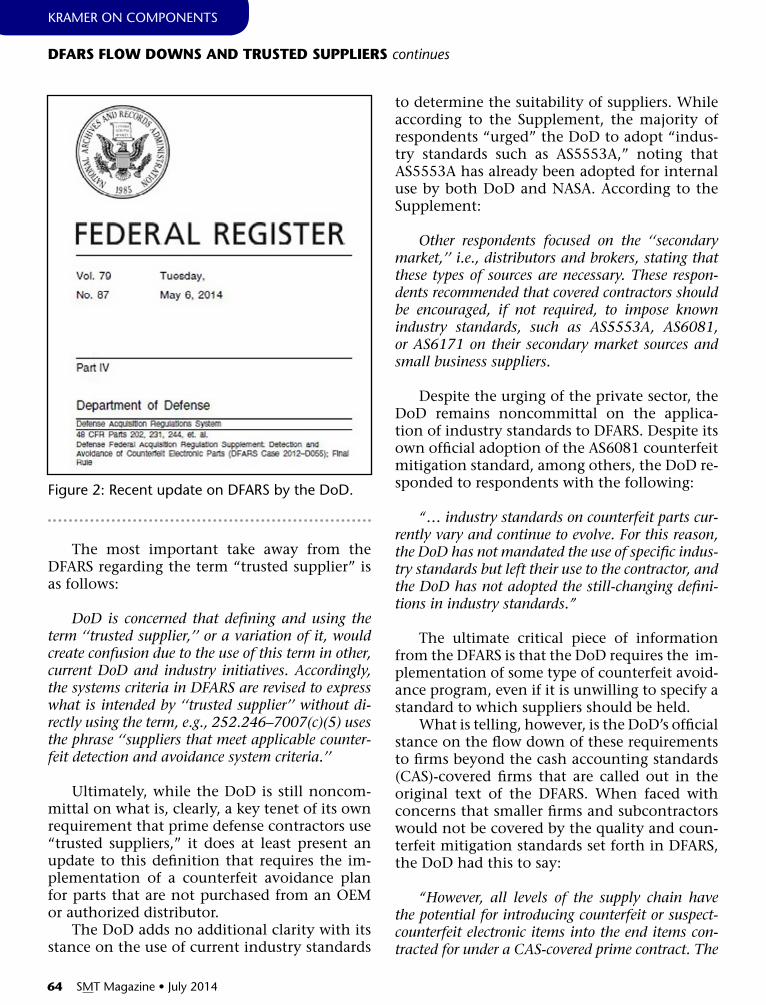
64 SMT Magazine • July 2014
The most important take away from the DFARS regarding the term “trusted supplier” is as follows:
DoD is concerned that defining and using the term ‘‘trusted supplier,’’ or a variation of it, would create confusion due to the use of this term in other, current DoD and industry initiatives. Accordingly, the systems criteria in DFARS are revised to express what is intended by ‘‘trusted supplier’’ without di-rectly using the term, e.g., 252.246–7007(c)(5) uses the phrase ‘‘suppliers that meet applicable counter-feit detection and avoidance system criteria.’’
Ultimately, while the DoD is still noncom-mittal on what is, clearly, a key tenet of its own requirement that prime defense contractors use “trusted suppliers,” it does at least present an update to this definition that requires the im-plementation of a counterfeit avoidance plan for parts that are not purchased from an OEM or authorized distributor.
The DoD adds no additional clarity with its stance on the use of current industry standards
to determine the suitability of suppliers. While according to the Supplement, the majority of respondents “urged” the DoD to adopt “indus-try standards such as AS5553A,” noting that AS5553A has already been adopted for internal use by both DoD and NASA. According to the Supplement:
Other respondents focused on the ‘‘secondary market,’’ i.e., distributors and brokers, stating that these types of sources are necessary. These respon-dents recommended that covered contractors should be encouraged, if not required, to impose known industry standards, such as AS5553A, AS6081, or AS6171 on their secondary market sources and small business suppliers.
Despite the urging of the private sector, the DoD remains noncommittal on the applica-tion of industry standards to DFARS. Despite its own official adoption of the AS6081 counterfeit mitigation standard, among others, the DoD re-sponded to respondents with the following:
“… industry standards on counterfeit parts cur-rently vary and continue to evolve. For this reason, the DoD has not mandated the use of specific indus-try standards but left their use to the contractor, and the DoD has not adopted the still-changing defini-tions in industry standards.”
The ultimate critical piece of information from the DFARS is that the DoD requires the im-plementation of some type of counterfeit avoid-ance program, even if it is unwilling to specify a standard to which suppliers should be held.
What is telling, however, is the DoD’s official stance on the flow down of these requirements to firms beyond the cash accounting standards (CAS)-covered firms that are called out in the original text of the DFARS. When faced with concerns that smaller firms and subcontractors would not be covered by the quality and coun-terfeit mitigation standards set forth in DFARS, the DoD had this to say:
“However, all levels of the supply chain have the potential for introducing counterfeit or suspect-counterfeit electronic items into the end items con-tracted for under a CAS-covered prime contract. The
KRAMER on CoMPonEnTS
figure 2: Recent update on DfARS by the DoD.
DFARS FloW DoWNS AND TRuSTED SuPPlIERS continues

July 2014 • SMT Magazine 65
prime contractor cannot bear all responsibility for preventing the introduction of counterfeit parts. By flowing down the prohibitions against counterfeit and suspect counterfeit electronic items and the re-quirements for systems to detect such parts to all subcontractors that provide electronic parts or as-semblies containing electronic parts (without regard to CAS-coverage of the subcontractor), there will be checks instituted at multiple levels within the sup-
ply chain, reducing the opportunities for counterfeit parts to slip through into end items.”
What does this mean for businesses that supply components to prime defense contrac-tors and other CAS-covered firms?
Ultimately, as requirements are flowed down from larger firms who wish to reduce their own liability, smaller firms will be required to adapt
KRAMER on CoMPonEnTS
DFARS FloW DoWNS AND TRuSTED SuPPlIERS continues
figure 3: Authenticating purchased product flow down.

66 SMT Magazine • July 2014
to the new market conditions in the defense sector. This will ultimately take the form of an industry-wide push towards certification, as larger firms attempt to mitigate liability and smaller suppliers fight to keep the business of the primes and other large firms.
The main points of the DFARS that should be considered are as follows:
• Firms that already maintain a certification to the most recent standards such as AS5553A and AS6081 should both maintain these levels of counterfeit mitigation and encourage other firms to do so• Those suppliers which are compliant, but not certified to up-to-date standards should strongly consider certification in order to keep pace with the flow down of DFARS, as well as for the limiting of liability• Firms which do not maintain a counterfeit avoidance program should immediately
develop a program that is, at the very least, compliant with current standards, and should rapidly pursue certification to these standards. This is both for the good of the firm and for the good of the ultimate customer, the Warfighter.
These points should be considered by all firms who wish to remain in the defense sup-ply chain—hopefully the application of these standards will lead to the eventual eradication of the current counterfeit epidemic. SMT
Todd Kramer is CEo of Secure Components LLC, an AS6081 & AS9120 certified independent distributor of electronic and mechanical components to the aerospace, defense, and high-
reliability industries. To contact Kramer or to read past columns, click here.
KRAMER on CoMPonEnTS
DFARS FloW DoWNS AND TRuSTED SuPPlIERS continues
realtimewith.comCliCk
To View
Video Interview
Eric Miscoll, managing principal of Charlie Barnhart & Associates, discusses the trends facing the electron-ics industry, and he explains some of the newest terms that have been adopted by electronics manufacturers.
A Glimpse of the Futureby Real Time with...IPC APEX EXPO 2014


68 SMT Magazine • July 2014
SMTonline Market News Highlights
IoT Market to Reach $1,423 Billionby 2020The value of internet of Things (ioT) market was worth $1029.5 billion in 2013, and is expected to reach $1,423.09 billion by 2020, at an estimated CAgR of 4.08% from 2014–2020.
Graphene Markets to Top $390 Millionin 2024new research by iDTechEx in the report “gra-phene Markets, Technologies and opportuni-ties 2014–2024” shows that graphene markets will grow from around $20 million in 2014 to more than $390 million in 2024, at the material level.
Printing Technologies Extend toPE ComponentsPrinted electronics uses graphic arts techniques such as screen printing or inkjet, to print electronic and photonic devices by using conducting or di-electric inks that results in the development of ac-tive or passive devices such as resistors or thin film transistors (TfT).
Positive outlook Develops forGlobal EconomyPaul A. Laudicina, founder of the fDi Confidence index, notes, “Despite racking volatility and eco-nomic uncertainty on a global scale, the findings from the 2014 fDiCi suggest that a corner is be-ing turned. Corporations sitting on massive cash reserves are increasingly confident they can parlay these into productive investments with attractive returns.”
EMS Market Driven by Demandfor Testing ServicesThe testing services provided by EMS provid-ers are dependent on the solutions required by oEMs and the vertical to which they cater. The outsourcing of testing services to EMS provid-ers will increase due to innovation in consumer electronics products. The market is driven by strong demand for such services from the tele-communication and consumer electronics in-dustries.
The Conference Board Sees Strong,Steady Job GrowthThe underlying hiring trend, especially in profes-sional services, is encouraging, with more good news expected through the summer and into the fall. More jobs means more pay checks, lifting sen-timent and resulting in still more consumer buying.
Industrial Robotics Market to SeeSteady 6.4% CAGRin United States alone the sale of industrial robotics for manufacturing use grew by 44% during 2011, indicating that the industrial robotics market is a correlant to the overall revitalization of the produc-tion base in the U.S. and a an important compo-nent of the general economic performance of the country.
Energy Capacity of Energy StorageApplications: CAGR of 71%According to a recent report from navigant Re-search, the annual energy capacity of advanced batteries for utility-scale energy storage applica-tions will grow from 412 megawatt-hours (MWh) in 2014 to more than 51,200 MWh in 2023, at a compound annual growth rate of 71%.
Automotive Electronics Market at$77B by 2020The automotive under-the-hood ECU electronics market is estimated to have been worth $44.8 bil-lion in 2013 and is forecast to grow to $77 billion in 2020, a CAgR of 8%. Semicast forecasts global light vehicle production volumes to grow over this period from 82 million to 106 million. However, more than 40% of the increase in global light ve-hicle production is forecast for China alone.
3D Printing: The Making of a $7B Market The market has huge potential, but is still embry-onic in terms of development, with main players taking their first steps by 3D printing conductive and insulating materials into a single object. 3D printed electronics, including 3D printed transis-tors, will not be fully realised within 10 years, but some emerging medical applications will be com-mercialised well before 2025.
68 SMT Magazine • July 2014

Become part of a global network of trusted
industry sources
Differentiate your company from the competition
Reduce your costs and labor for quality assurance audits
and minimize material qualification cycle time
Ensure product quality throughout your supply chain
Explore the IPC Validation Services website and learn how you can win with VS.
IPC Validation Services takes certification to the product and enterprise level. Through two
new programs — the Qualified Products List (QPL)
and the Qualified Manufacturers List (QML) —
IPC Validation Services has expanded the value,
quality and risk mitigation already offered by
IPC’s standards and training.
www.ipcvalidation.org

70 SMT Magazine • July 2014
by Rachel Miller-Short
THE SHoRT SCooP
CoLUMn
More Stencil Questions(and the Answers!)
My March Short Scoop column, 10 Com-mon Stencil Questions, brought in a slew of new questions from customers. Do you know the answers?
1. What are my fiducial choices and how do they differ?
Yes, stencils require fiducial markings to make sure the stencils are aligned correctly to properly print the pattern, as most people know. What they might not know is that there are ac-tually several types of fiducials, and when you select a stencil, you must choose one of them.
The fiducial choices available today depend
on the stencil manufacturer you use and/or your own requests, but truthfully, there really are only two predominate types. One is half-etched and filled, which have an etched pocket in the stencil at the fiducial location that is then filled with a black epoxy. Ultimately, these of-fer one of the strongest contrasts for the visual printer cameras, but they are an older technol-ogy and often, the epoxy falls out at the least opportune time.
The other predominate type is a laser tat-tooed fiducial, which is a relatively newer tech-nology. These are applied by a laser (usually the same one that cuts the apertures for a laser sten-cil). In this technology, the laser truly burns the

We offer a full range of auditing services for bothbuyers and sellers, backed by 35 years of industry experience.
We’d love to talk with you about getting to the next level.
A few words from our clients.
AN AUDIT ING COMPANY
" ...with Rob’s years of experience performing audits and his vast knowledge, I believe Wizlogix and my end customers are benefiting. Moving forward, we will continue to explore more opportunities and collaborations with Next Level PCB services in the future."
Shawn NgDirector/Co-Founder, Wizlogix Pte Ltd
Steve RobinsonPresident, APCT, Inc.
"...Not only did we gain the potential of a valued new customer, we also had the eyes of a skilled PCB expert reviewing our operations and systems providing some positive and constructive feedback."
View full testimonial
View full testimonial
Say hello to us
(360) 531-3495www.nextlevelpcb.com

72 SMT Magazine • July 2014
fiducial to the stencil. The benefits are that it lasts forever and the epoxy doesn’t fall out. La-ser tattooed fiducials provide the tightest loca-tion tolerance of any fiducial and most com-panies are moving toward this technology. It is imperative to note, however, that the dark-ness of the laser fiducials have varying contrasts from one stencil to another. This is usually due to the material type, the pattern density of the stencil, laser type, and several other factors. I mention this because some printers struggle with the contrast that is less than what they might have had previously in the half-etched and filled fiducials.
2. What CAD information and files are needed to make my stencil and how will I re-ceive my check plots?
These are very important questions so that manufacturers know what to expect and don’t waste time or effort preparing something that isn’t usable by the stencil manufacturer. Addi-tionally, they don’t have to go back to a format that is different from what is usually done. We use IGI and Valor, which are software systems that can custom design each stencil. The types of files we need include:
• Import file types: Gerber (274x), ODB++, dxf/dwg and gdsII• Export file types: Gerber (274x), ODB++, dxf/dwg, gdsII and pdf• Types of files needed to create a stencil: Gerber (274x), ODB++, dxf/dwg, gdsII and pdf
It’s always best to ask this question at the initial meeting with your stencil manufacturer to make sure your systems are compatible.
3. What types of quality inspection are per-formed on my stencils and when are they done?
QC checks can vary quite drastically from one stencil vendor to another. High-quality stencil manufacturers usually have QC checks starting from the very beginning when a new order comes in, which ensures that the order is processed correctly, the CAD files are inter-preted and modified correctly, and customer re-quirements are clearly understood. In addition, a completed stencil usually goes through a QC process to ensure that all of the apertures are present. This entails a scan of the stencil to com-pare it to the Gerber file, thus making sure that all necessary apertures are present. Especially with electroformed or step stencil technologies, the stencil thickness needs to be verified to see that the targeted thickness or thicknesses have been achieved.
Final QC checks usually include verifica-tion of aperture size, either on certain selected apertures or apertures in certain defined geog-raphies of the stencil, image run-out, fiducial count and darkness, surface roughness, frame type and flatness, and any additional QC checks that the manufacturer or customer deems nec-essary. Some customers require a Certificate of Compliance to accompany purchased stencils. Usually included in a Certificate of Compliance are specifications such as thickness, certain ap-erture size measurements, and run-out.
CoLUMn
figure 1: Duraglide squeegee blades yield near perfect solder brick deposits over tens of thousands of print cycles.
MoRE STENCIl QuESTIoNS (AND THE ANSWERS!) continues

July 2014 • SMT Magazine 73
4. What is an average blade life and how often should I change them?
We seem to get a lot of blade questions. Blades are a key component to the print pro-cess.
Through many conversations with cus-tomers and time on SMT lines, it has become apparent to me that blades are not getting the attention they should be. The right blade, when paired with a stencil in an application, can make the difference between a success-ful print and a print that needs substantial rework.
That said, in general, standard OEM blades are sufficient for most print applications as long as they are changed and inspected for de-fects regularly. As a rule of thumb, an SMT line running 1.5–2 shifts, 5–6 days a week, with a couple of different blades or blade size chang-es during the course of a week, should have the blades changed every 3–4 months. At that point, the blades will have produced enough
prints to dull the blade edge, which has prob-ably been nicked or dinged a couple of times already, but not severely enough to cause them to be replaced. Most OEM blades cost under $55 a set, and some companies can even arrange an automatic replacement program. The negative impact on your process and product that results from not changing the blades regularly certain-ly costs more than $55.
In a future column, I will explore questions regarding the possible causes of poor printing results. SMT
MoRE STENCIl QuESTIoNS (AND THE ANSWERS!) continues
CoLUMn
Rachel Miller-Short is global vP of sales at Photo Stencil LLC. To contact the author, or to read past columns, click here.
realtimewith.comCliCk
To View
Video Interview
DEK’s Clive Ashmore and Editor Kelly Dack explore the ways DEK handles automotive customers’ challenges with device miniaturization, and why the lessons learned in the mobilephone segment don’t necessarily translate into the automotive world.
DEK Deals with Automotive Device Miniaturization
by Real Time with...IPC APEX EXPO 2014

74 SMT Magazine • July 2014
SMTonline Supplier/New Product News Highlights
GoEPEl’s GATE Extends Partnershipin ChinagoEPEL electronic extends its strategic partner-ship program goEPEL Associated Technical Experts (gATE) in the Asian market by adding the Chinese company Sifo as a new member.
CircuitWorks overcoat Pen Releasedby Intertronicsintertronics’ recent launch of the CircuitWorks overcoat Pen is expected to make coating of PCBs especially convenient during manufacture, rework, and prototyping, by enabling the replacement of permanent solder resist or mask over repaired ar-eas, or where it is damaged or missing.
Electrolube Coating Earns SMT ChinaVISIoN AwardElectrolube, the leading manufacturer of special-ist chemicals for the electronics, automotive, and industrial manufacturing industries, announced that its UvCL Uv cure conformal coating has won the 8th SMT China vision Award in the Conformal Coatings category.
Essemtec Strengthens Partnershipwith ACI Technologies The company has renewed its partnership with ACi Technologies inc. (ACi) and will provide ACi with a complete SMT line. in return, Essemtec will use ACi’s facility for demos, seminars, training, and more.
Nordson Expands in Colorado;To Build New Facility“We continue to see outstanding global growth opportunities for innovative components, devices and custom oEM solutions related to precision flu-id management and delivery of biomaterials,” said george Porter, vice president and general manager for medical product lines.
New Paste Retainer Design fromTransisiton AutomationTransition Automation inc. has unveiled a new paste retainers design which improves the man-
agement of solder paste within the printing area. The new product, SPR, helps eliminate leakage of solder paste out of the print area by way of a floating spring supported paste re-tainer attached to the end of the squeegee holder.
Manncorp Enhances Dip Soldering;Debuts New ModelsAuto-Dip models feature programmable preheat and dip-height settings and include an adjust-able, finger-type PCB holder that firmly grips the edges of the board throughout the soldering cycle. This flexible design is especially useful for heavy component-laden assemblies and can also accept customized pallets of very small, irregular-ly-shaped PCBs.
universal Science B.V. Invests inEssemtec MachinesUniversal Science, the international market leader in thermal management in electronics assemblies and LED lighting, has further expanded its SMT production line with the investment in an Essem-tec Tucano Plus screenprinter.
Speedline launches NewElectrovert ElectraThe new Electrovert Electra by Speedline Technol-ogies is the next generation in wave soldering sys-tems, offering new features and enhanced perfor-mance that make it the most state-of-the-art wave soldering system to be launched into the market-place to date, according to geoff Klein, Electrovert general manager.
Panasonic Selects Repstronics asSales Rep in Mexico“Repstronics’ team of experienced, bilingual en-gineers, as well as their dedicated Technical Cen-ter in guadalajara, are a great resource for help-ing manufacturers in Mexico find the right elec-tronics assembly and software solutions for their challenges,” said Mark Ragard, general manager, Electronics Assembly Sales.
74 SMT Magazine • July 2014


76 SMT Magazine • July 2014
ARTiCLE
AbstractThe explosive growth of personal electronic
devices, such as mobile phones, tablets, and personal music devices, has driven the need for smaller and smaller active and passive electrical components. Not long ago, 0201 passives were seen as the ultimate in miniaturization, but now we have 01005 passives with rumors of even smaller sizes not far behind. For active compo-nents, array packages with 0.4 mm pitch are virtually a requirement for enabling the many features in modern portable electronic devices. To meet the challenge of stencil printing small-er stencil apertures, there is an increased inter-est in using finer particle-sized solder pastes to improve transfer efficiency. The smaller particle size results in a large surface area-to-volume ra-tio that challenges the solder paste’s flux to ef-fectively perform its fluxing and oxidation pro-
tection action. The potential resulting surface oxidation can lead to voiding, graping, head-in-pillow, and other defects.
The combination of higher lead-free process temperatures, smaller print deposits, and tem-perature restraints on electrical components has created several challenges. Two in particular are obtaining consistent volume in the printed sol-der paste deposit and minimizing the oxidation of the solder powder in the small deposit during reflow. Solder pastes comprised of finer particle solder powders may help with stencil printing, but the increased surface oxide associated with finer powders may also reduce the reflow pro-cess window. The focus of this paper is to pro-vide a statistical comparison of the transfer ef-ficiency of different solder powder particle sizes, specifically types 3, 4, 5, and 6, and to visually observe post-reflow results in both optimal and harsh conditions.
IntroductionBack to the basics, or the fundamentals, is
a term often heard in relation to sports teams when they lose sight of the basic foundations
by Edward BriggsinDiUM CoRPoRATion
Meeting Future Stencil Printing Challenges with Ultrafine Powder Solder Pastes
As originally published in the 2014 International Conference on Soldering and Reliability Proceedings.

www.smta.org
2014 Event Schedule
SMTA Headquarters |5200 Willson Road| Suite 215| Edina, MN55424 | [P] 952-920-7682 | [F] 952-926-1819
Facebook: Facebook.com/SMTAssociation LinkedIn: Find us under groups, “Surface Mount Technology Association”
July 15 & 22 Webtorial: Failure Analysis: Lessons Learned in Manufacturing Instructor: Martin Anselm, Ph.D., Universal Instruments Corp. July 17 Ohio Expo and Tech Forum Doubletree Hotel, Independence, OH July 17 Guadalajara Expo and Tech Forum Real Inn, Ciudad Juarez, Mexico August 12 Philadelphia Expo and Tech Forum Crowne Plaza Philadelphia, Cherry Hill, NJ August 14 West Penn Expo and Tech Forum Doubletree Monroeville, Monroeville, PA August 19 & 26 Webtorial: SMT for Movers, Shakers, and Rainmakers Instructor: Ray Prasad, Ray Prasad Consultancy Group September 9 Capital Expo and Tech Forum Johns Hopkins University, Laurel, MD September 10 Webinar: Power and High Temperature Electronics Manufacturing Instructors: Dr. Chris Hunt, NPL Bob Willis, NPL Defect Database Coordinator September 11 & 18 Webtorial: Evaluating the Performance of Conformal Coatings Instructor: Doug Pauls, Rockwell Collins September 18 Empire Expo and Tech Forum Radisson Hotel, Rochester, NY September 18 - 19 Medical Electronics Symposium Organized by SMTA, iNEMI & MEPTEC Marylhurst University, Portland, OR
September 28 - October 2 SMTA International Conference & Exhibition Co-located with IPC Fall Standards Development Committee Meetings Donald Stephens Convention Center, Rosemont, IL October 14 Austin (CTEA) Expo and Tech Forum Norris Conference Center, Austin, TX October 15 Long Island Expo and Tech Forum Islandia Marriott, Long Island, NY October 16 & 23 Webtorial: Improving Mechanical, Electrical and Thermal Reliability of Electronic Assemblies Instructor: Tim Jensen, Indium Corporation October 21 Connecticut Expo and Tech Forum Waterbury Marriott, Waterbury, CT October 23 Intermountain Expo and Tech Forum University of Utah, Salt Lake City, UT November 6 LA/Orange County Expo and Tech Forum Grand Event Center, Long Beach, CA November 11-13 International Wafer-Level Packaging Conference (IWLPC) DoubleTree by Hilton Hotel, San Jose, CA November 18-20 High-Reliability Cleaning and Conformal Coating Conference Organized by SMTA & IPC Chicago Marriott Schaumberg, Schaumburg, IL November 19 Arizona Expo and Tech Forum Phoenix Marriott, Tempe, AZ December 4 Space Coast Expo & Tech Forum Park Inn by Radisson, Kissimmee, FL

78 SMT Magazine • July 2014
MEETING FuTuRE STENCIl PRINTING CHAllENGES continues
ARTiCLE
of playing the game. In the SMT process, this may not necessarily be due to losing sight of the basic fundamentals, but because the game itself continues to evolve. As the trend towards miniaturization continues, a process that was successful in the past may suddenly present un-acceptable results due to the decreasing size of the stencil apertures required to print ultrafine solder paste deposits. In an earlier paper titled “Process Guidelines to Ensure Optimal SMT Electronics Assembly” (Edward Briggs and Ron Lasky SMTAI Toronto, May 2012), I discussed solder paste storage and handling; process set-up, including the importance of gasketing and registration; solder paste attributes; reflow pro-cesses; newer SMT technologies; and the data collection methods for characterizing the sten-cil printing process to meet this evolution. The focus of this paper is to single out one of those considerations—powder particle size (powder types) and its effect on the stencil printing pro-cess. In order to focus on particle sizes, many variables as possible were eliminated and the data analyzed using solder paste inspection equipment. A physical observation will also be made of the reflowed results. Finer powder par-ticles mean an increase in surface oxide and can create challenges for reflow.
Stencil Printing and Area Ratio and Transfer Efficiency
In regard to stencil printing success, the two most critical parameters are the area ratio (AR) and transfer efficiency. Area ratio is the area of the stencil aperture opening divided by the area of the aperture side walls. Figure 1 shows
an area ratio schematic for a circular aperture. Simplifying the calculation shows that the area ratio (AR) is the diameter (D) of the circle di-vided by 4 times the stencil thickness (t): AR = D/4t. The result is the same for square apertures, with the diameter (D) now equal to a side of the square. For the AR of a rectangular aperture, the formula is a little more complicated: ab/2(a+b)t, where a and b are the sides of the rectangle.
It is widely accepted in the industry that the AR (area ratio) must be 0.66 or greater to be suc-cessful in the stencil printing process. Histori-cally, experience has shown that if AR < 0.66, the transfer efficiency will be low and inconsis-tent. Transfer efficiency is defined as the volume of the actual solder paste deposited divided by the calculated volume. Measuring the effect of AR on fine feature printing will be an important part of our experiment.
The Experimental DesignThe focus of this printing experiment was to
differentiate transfer efficiency and consistency between powder types. Therefore, in an effort to diminish the number of variables, the same stencil, squeegee blades and printer parameters were utilized (Figure 2).
A 4 mil thick laser cut stencil, 250 mm squeegee with edge guards, foilless clamps, and landscape vacuum support blocks were used on the stencil printer. Figure 2 depicts the printer
figure 1: Definition of the area ratio for a circular stencil. figure 2: Printer settings.

July 2014 • SMT Magazine 79
MEETING FuTuRE STENCIl PRINTING CHAllENGES continues
ARTiCLE
settings utilized for the experiment. Each sol-der paste was printed at 50 mm/s with a blade pressure of 4.4kg, 5 mm/s separation speed, and separation distance of 2 mm. The underside stencil-wipe method was used only during the one-hour pause W/D/V (wet/dry/vacuum).
A test vehicle (Figure 3) was selected with fo-cus on 6, 7, 8, 9, 10, 12 mil circles and squares, as well as 0201 pads in both solder mask defined (SMD) and non-solder mask defined (NSMD) pads. Four powder types were evaluated: types 3, 4, 5, and 6 in no-clean and water soluble flux formulations. Response to pause was measured by continuous printing 20 times, pausing for 1 hour, and printing 6 more times. A wet/dry/vacuum stencil wipe was incorporated imme-diately after printing the first 20 PWBs. A Koh Young KY-3020T laser scanning system was used to measure the volume of the stencil printed de-posits. In all, 1,386,500 data points (solder paste deposits) were collected.
Figure 4 shows the component identifica-tion and the area ratio associated with it.
Printing ResultsGauge Variability Chart for Volume (%)
Figure 5 represents a broad view of the re-sultant test data. The y axis of the upper graph indicates the transfer efficiency in volume %, with 100% being the target. The bottom graph indicates the standard deviation of the process; a smaller standard deviation indicates a more consistent process. Included in the test were a number of 0201 and 12 mil chip scale package
(CSP) test pads that are not depicted. The solder paste deposits on these pads were well-printed regardless of powder and flux type and were therefore excluded from further investigation. The data in Figure 5 reveals that the smallest test aperture (6 mil) did not print well for all powder types or flux vehicles. The area ratio is quite small (0.375) for the 6 mil aperture and the results were inconsistent.
Variability Gauge Component ID=S07_SMD Variability Chart for Volume(%)
A dramatic improvement occured with 7 mil apertures that deserved further investigation, notably between the water soluble and no-clean flux formulations. Figure 6 shows the improve-ment in more detail by expanding the view of the 7 mil aperture and breaking out the data be-fore and after the 1-hour pause. Note that a stan-dard deviation <10%, with the exception of a few outliers which exhibits a controlled process, was achieved specifically with the Indium8.9 no-clean flux chemistry. The area ratio for the
figure 3: Test vehicle.
figure 4: Pad labels, description, and associated area ratios.
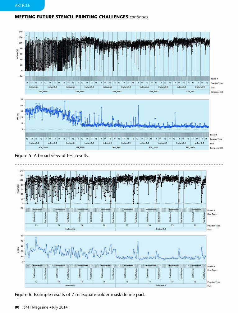
80 SMT Magazine • July 2014
MEETING FuTuRE STENCIl PRINTING CHAllENGES continues
ARTiCLE
figure 5: A broad view of test results.
figure 6: Example results of 7 mil square solder mask define pad.

July 2014 • SMT Magazine 81
MEETING FuTuRE STENCIl PRINTING CHAllENGES continues
ARTiCLE
7 mil aperture is 0.4375. The transfer efficiency was near the target (100%) and improved as the powder type moved toward type 6. Type 5 ex-hibited the best results; a narrow distribution in volume percent and low standard deviation ex-cept after first pause. It is important to note that the significant drop in transfer efficiency after the 1-hour pause is not consistent with previ-ous experiments; this is attributed to a very low humidity (<10%) and had a dramatic effect on the first print after sitting on the stencil for one hour, for all solder pastes tested.
Looking at the first chart in Figure 7, it can be seen that the mean transfer efficiency favors the no-clean flux. The water soluble flux in the Indium6.4 solder paste was more erratic, giving more insufficient, as well as excessive, solder
paste deposits. The second chart reveals that most of this inconsistency occurs with the 6 mil aperture. This result is consistent with previous experience. The rosin/resin bases found in most no-clean fluxes increase the material’s tacky properties (adhesive and cohesive attractions) of the solder pastes. When releasing from the stencil aperture, adhesion of the solder paste to the PCB pad helps pull the paste from the sten-cil aperture as the PCB is lowered from the sten-cil. This is especially true for the smaller pads, as there is very little surface area for the paste deposit to cling to. The cohesive forces or at-traction of the flux-coated powder particles to one another are also increased. These cohesive forces help the paste release from the stencil walls and retain shape of the stencil aperture after printing.
Variability GaugeVariability Chart for Volume (%)
Figure 8 shows stencil printing results for square vs. circular apertures. The results for 7 and 8mil square apertures are designated S07 and S08 respectively, and those for 7, 8, and 9 mil circular apertures are C07, C08, and C09 respectively. The 7 mil square aperture exhibits acceptable results with less than10% standard deviation and good volume percent aperture filling. There were, however, a couple of outli-ers after the one-hour pause. The 7 mil circular aperture exhibits erratic behavior as shown by its high standard deviation. The 8 mil circular is comparable to the 7 mil square with much smaller standard deviation and good volume percent aperture filling. Consistent with past experience for the same area ratio, the square aperture with radius corners produced deposits with more volume of solder paste—21% more in this test.
Variability GaugeVariability Chart for Volume (%)
Perhaps one of the more dramatic changes in transfer efficiency and standard deviation is noted for the same aperture size and shape, but with pads that differ in solder mask. Sol-der mask defined pads exhibit far better results than the non-solder mask defined or copper defined. This result is also consistent with pri-
figure 7: Mean of volume percent by flux and flux/aperture interaction.

82 SMT Magazine • July 2014
ARTiCLE
MEETING FuTuRE STENCIl PRINTING CHAllENGES continues
figure 8: Circles vs. squares.
figure 9: Solder mask defined vs. non-solder mask defined (copper defined) pads.
Medical Electronics Symposium 2014September 18 & 19, 2014
MARYLHURST UNIVERSITY • PORTLAND, OR
Oregon BioscienceAssociation
INEMI, MEPTEC, and SMTA have joined forces to host this international confer-ence, focusing on advances in electronic technologies and advanced manufacturing, specifically targeting medical and bioscience applications. Previously, MEPTEC’s and SMTA’s conferences were held in Phoenix, Arizona and Milpitas, CA, respectively, drawing technology experts, entrepreneurs and service providers that work in this niche technology space. Typi-cal applications within this space involve implantable defibrillators, neurostimula-tors and drug delivery, inter-ventional catheters, pillcams, ultrasound transducers, hear-ing aids, biosensors, micro-fluidics, wireless communica-tions, as well as future diag-nostic and treatment solu-tions that may use stretchable electronics, microelectrome-chanical systems (MEMS) or nanoelectromechanical sys-tems (NEMS). ◆
Marylhurst University, founded in 1893, is Oregon’s oldest Catholic university, and the first liberal arts college for women established in the Northwest.
Multiple Track Topics Include:
n Track 1: Components and Designs for Higher Density Functionalities
This track will focus on advances in electronics components and designs that can make current medical electronics ever more miniaturized with more functionality and at lower power.
n Track 2: Solutions for Best-in-Class Assembly and Volume Manufacturing
This track will focus on critical methods and protocols to ensure that the production of Class II and III medical electronics is conducted in the most effective, efficient and quality-controlled way with full traceability and zero defects.
n Track 3: Next Generation Microelectronics for Changing Healthcare Markets
This track will focus on advances in next generation, revolutionary microelectronics for medical devices and applications that solve technology challenges and are aligned with solutions for new healthcare models.
REGISTER ONLINE TODAY AT SMTA.ORG/MEDICAL
KEYNOTES
Digital Health and the Connected Consumer
Matthew HudesU.S. Managing Principal,
Biotechnology
Deloitte Health Sciences
Ensuring Quality Medical Devices Meet Regulatory
Scrutiny in the Face of Industry Cost Pressures
Mike TendickHealthcare/Life Sciences
Market Sector Vice President
Plexus
What Can Medical Devices Leverage from Consumer Electronics?
Chandra SubramaniamVice President CRDM
Research & Development
Medtronic
GOLD SPONSOR GOLD SPONSOR SILVER SPONSOR SILVER SPONSOR LUNCH SPONSOR FLASH DRIVE SPONSOR

84 SMT Magazine • July 2014
or experience and attributed to an increase in surface area for the solder paste deposit to ad-here to when solder mask define pads are used. However, the challenge with solder mask at these small apertures is the registration of the solder mask to the pad. Achieving this precise registration can become difficult for the board supplier.
Reflow ProfileImproving the stencil printing process with
finer particle solder pastes affects the reflow process, often minimizing the reflow process window for acceptable results. As the particle size decreases, the total surface area for the same volume of solder paste increases. This increase in total surface area also means an increase in total surface oxide and increases the demand on the flux to remove them.
The demand on the flux is further chal-lenged as the reason for selecting a finer particle solder paste to print into a smaller stencil aper-
MEETING FuTuRE STENCIl PRINTING CHAllENGES continues
ARTiCLE
figure 10: Relationship of surface area to available flux as aperture size decreases.
figure 11: optimal reflow profile.
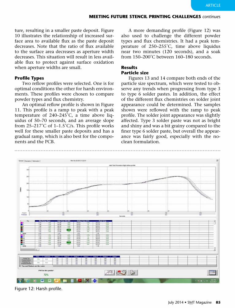
July 2014 • SMT Magazine 85
MEETING FuTuRE STENCIl PRINTING CHAllENGES continues
ARTiCLE
figure 12: Harsh profile.
ture, resulting in a smaller paste deposit. Figure 10 illustrates the relationship of increased sur-face area to available flux as the paste deposit decreases. Note that the ratio of flux available to the surface area decreases as aperture width decreases. This situation will result in less avail-able flux to protect against surface oxidation when aperture widths are small.
Profile TypesTwo reflow profiles were selected. One is for
optimal conditions the other for harsh environ-ments. These profiles were chosen to compare powder types and flux chemistry.
An optimal reflow profile is shown in Figure 11. This profile is a ramp to peak with a peak temperature of 240–245˚C, a time above liq-uidus of 50–70 seconds, and an average slope from 25–217˚C of 1–1.5˚C/s. This profile works well for these smaller paste deposits and has a gradual ramp, which is also best for the compo-nents and the PCB.
A more demanding profile (Figure 12) was also used to challenge the different powder types and flux chemistries. It had a peak tem-perature of 250–255˚C, time above liquidus near two minutes (120 seconds), and a soak from 150–200˚C between 160–180 seconds.
ResultsParticle size
Figures 13 and 14 compare both ends of the particle size spectrum, which were tested to ob-serve any trends when progressing from type 3 to type 6 solder pastes. In addition, the effect of the different flux chemistries on solder joint appearance could be determined. The samples shown were reflowed with the ramp to peak profile. The solder joint appearance was slightly affected. Type 3 solder paste was not as bright and shiny and was a bit grainy compared to the finer type 6 solder paste, but overall the appear-ance was fairly good, especially with the no-clean formulation.

86 SMT Magazine • July 2014
MEETING FuTuRE STENCIl PRINTING CHAllENGES continues
ARTiCLE
A couple of observations can be made from Figures 15 and 16. First, a dramatic effect is seen in the type of reflow profile; the harsh environ-ment imposed by the hotter, longer profile ex-hausts the flux activity and oxidative resistance. The solder joints show observable effects of flux exhaustion giving an appearance of some de-
wetting and graping (oxidized solder particles that do not coalesce into the solder joint). The type of reflow profile used shows the effect on the solder joints, as seen in the observable re-sults.
The second observation is in regards to flux formulation. Note that a more dramatic ef-
figure 13: 0201 components and 6 mil dot, water soluble paste (indium6.4): type 3, top; type 6, bottom.
figure 15: 0201 components and 6 mil dot, water soluble indium6.4 type 6: ramp to peak, top; soak, bottom.
figure 14: 0201 components and 6 mil dot, no-clean solder paste (indium8.9): type 3, top; type 6, bottom.
figure 16: 0201 components and 6 mil dot, no-clean indium8.9 type 6: ramp to peak, left; soak, right.


88 SMT Magazine • July 2014
fect is observed between the ramp to peak and soak profiles for the water soluble formulation. This result is consistent with prior experience and due to lower oxidation resistance of water soluble fluxes. It is true that water soluble for-mulations are more active, but the oxidation resistance is poor in comparison to rosin/resin based no-clean formulations. Activity refers to the ability to remove existing surface oxides; oxidation resistance refers to the ability of the flux chemistry to prevent re-oxidation, which occurs later in the reflow process. Rosin/resin provides an excellent oxidative barrier, widen-ing the reflow process window. This is espe-cially true if a ramp to peak type profile is not attainable.
SummaryThe utilization of ultrafine solder powders
can improve transfer efficiency in the stencil printing process and effectively reduce the area ratio acceptance level to 0.50. Some con-tributing factors need to be considered such as square vs. circle and solder mask defined pads vs. copper defined to attain desireable results.
A trade-off when choosing ultrafine solder pastes is the premature flux exhaustion due to an increase in total surface oxide, and sensitiv-ity of the smaller paste deposit-utilized for the oven environment. The total heat excursion that the solder paste endures may need to be optimized. Striving for a ramp to peak type profile with a peak temperature 240–245˚C (SAC305), time above liquidus 45–60s, and an average ramp rate 1–1.5 ˚C/s is ideal. No-clean flux formulations provide more oxidation resis-tance than water soluble formulations and can widen a reflow process window, especially if a ramp to peak profile is not attainable. SMT
AcknowledementSpecial thanks to Eric Moen and Laserjob
for providing the stencil utilized in this study.
MEETING FuTuRE STENCIl PRINTING CHAllENGES continues
ARTiCLE
Ed Briggs is a green Belt Six Sigma certified technical support engineer with indium Corporation. To contact him, click here.
Thermal systems use heat to produce cold, and vice versa. To do so, a material must dissipate water vapor particularly well and quickly. A new method applies this property as a layer onto the components.
Refrigerators have the human body as an ex-ample: When we perspire, water evaporates on our skin and cools it. if the process is transferred to a vacuum, water evaporates at a few millibar and a temperature of 10 degrees. for the devices to continu-ously cool, vapor must be removed. This is achieved, for example, by an electric compressor.
An alternative is the thermal compressor; the operating power
is not electrical, but thermal. Heat pumps or chill-ers produce cold from heat, and vice versa. So far, however, these have not been able to prevail en-tirely over their electricity-powered counterparts.
Researchers at the fraunhofer institute for Solar Energy Systems iSE have now closed this gap. Their metal organic frameworks (Mofs) are well suited to absorb water vapor.
These layers can be directly applied without further auxiliary layers. in prototypes, Mofs are di-rectly crystallized onto metals. for other materials, such as ceramics, the scientists have accomplished this with binder-based coatings.
in both methods, the compo-nents of the device are immersed in a fluid containing the essential components of the material. The temperature needed for direct crystallization occurs only on the surface of the component, with minimum waste.
efficient thermal Cooling and Heating

July 10Conflict Minerals: Staying Current in a Changing LandscapeSanta Clara, CA, USA
August 20Southeast Asia High Reliability ConferencePenang, Malaysia
September 23–25IPC India Conference & Workshops at electronica & productronica India 2014Bangalore, India
September 28–October 2IPC Fall Standards Development Committee Meetingsco-located with SMTA InternationalRosemont, IL, USA
October 14–15IPC Europe High Reliability ForumDüsseldorf, Germany
October 28–30IPC TechSummitTM
Raleigh, NC, USA
November 18–20High-Reliability Cleaning and Conformal Coating Conferencesponsored by IPC and SMTASchaumburg, IL, USA
November 19Assembly & Reliability Conference Bangkok, Thailand
December 3–5International Printed Circuit and APEX South China Fair(HKPCA and IPC Show)Shenzhen, China
Questions? Contact IPC registration staff at +1 847-597-2861 or [email protected].
®
More Informationwww.ipc.org/events
SAVE THE DATES!Upcoming IPC Events
Strengthening & Advancing Electronics Manufacturing Globally

90 SMT Magazine • July 2014
aIPC Certifies Conflict Minerals Data Exchange Standard iPC-1755 was developed under a globally rec-ognized, industry-consensus standards process, which makes it easier for companies to use a single standard for all international operations. Support from AiAg, CfSi, and JEiTA highlight the global support for this effort. The association’s experience in developing industry-consensus data exchange standards helped standardize the data fields.
bVaritron Expands Presence; Acquires Altronics
“varitron and Altronics provide similar services, but also have complementary offerings intended for dif-ferent markets,” notes Michel farley, president of va-ritron group. “By pooling our expertise, we will be able to serve more customers and to provide added value in terms of volume with the aim of consolidat-ing the U.S. market and developing new niches.”
cNewbury Extends Free Parts listing for PCB Components
newbury Electronics is increasing its list of free parts for use in its PCB assembly to over 1,000 different components with immediate effect. The free parts scheme has been on trial for some time but has now been greatly extended to in-clude a wider range and more expensive com-ponents. This new approach to costing will ap-ply across the company’s PCB Train assembly operation.
dlower Mfg Volumes in Europe Hurt Incap’s Q1 Revenue
The group’s revenue was EUR 5.5 million, down approximately 51% year-on-year (Q1/2013: EUR 10.7 million) due to the decreased manufacturing volumes in the company’s factories in Europe.
Top TenNews Highlights from SMTonline this Month
90 SMT Magazine • July 2014
July 2014 • SMT Magazine 91
eFlextronics Expands Capabilities; Joins openDaylight
“With the advent of convergence, SDn and cloud, we see rapid shifts in the end-markets of our oEM customers. By leveraging open source platforms such as openDaylight, our oEM customers are able to get ahead of these shifts in the iT space,” said Dharmesh Jani, vP, Cloud Strategy.
fEnics Slovakia Receives ISo/TS 16949 Compliance
The plant has received an iSo/TS 16949 compli-ance letter from Bureau veritas stating its confor-mity with iSo/TS16949:2009—the Quality Sys-tem Requirement used in the automotive indus-try. “This is a remarkable achievement and proves that the people, processes, and systems are in place to meet most stringent quality requirements from the customers,” said Jari Utriainen, quality director.
gSMT’s Recovery Continues to Gain Momentum in Fy2014
SMT’s recovery continues to gain momentum. We are seeing increases in demand from most of our existing customers, in particular those from Eu-rope. There are new projects and new customers.
our outlook is positive. However, the escalating operating costs in China remain challenging.
hIncap Concludes Vaasa Factory Negotiation; Trims Jobs The negotiation process started on March 24, 2014 and total of 74 persons were invited to the negotiation process to discuss the actions to adjust the vaasa factory organization, operations, and cost structure to match the current and estimated situation.
iDeswell Suffers Sales Decline in Fy 2014 Deswell’s net sales for the fourth quarter end-ed March 31, 2014 were $7.9 million, down by 16.5% compared to net sales of $9.5 million for the same quarter ended March 31, 2013.
jEMS & oDM Vendors Benefit from High Capacity utilization
EMS and oDM services refer to the services for brand vendors except brand marketing, including product development and design, raw material procurement, manufacturing, assembly, and after-sales services.
July 2014 • SMT Magazine 91
smtonline.com for the latest SMT news—anywhere, anytime.

92 SMT Magazine • July 2014
for the ipc’s calendar of Events, click here.
for the smta calendar of Events, click here.
for the inEmi calendar, click here. for a complete listing, check out smt magazine’s full events calendar here.
SEMICoN West TechxPoT: Driving Automotive InnovationJuly 8–10, 2014San francisco, California, USA
ohio Expo & Tech ForumJuly 17, 2014Cleveland, ohio, USA
92 SMT Magazine • July 2014
E v E n T S
SusTech 2014July 24–26, 2014Portland, oregon, USA Advancements in Thermal Management 2014August 6–7, 2014Denver, Colorado, USA
Philadelphia Expo & Tech ForumAugust 12, 2014Cherry Hill, new Jersey, USA
CALEnDAR

July 2014 • SMT Magazine 93
advErtisEr indEx
PUBLiSHER: BARRy MATTIES
PUBLiSHER: RAy RASMuSSEN(916) 294-7147;
SALES MAnAgER: BARB HoCKADAy (916) 608-0660;
MARKETing SERviCES: ToBEy MARSICoVETERE (916) 266-9160; [email protected]
EDITORIAL:gRoUP EDiToRiAL DiRECToR: RAy RASMuSSEN(916) 294-7147;
MAnAging EDiToRS: lISA luCKE (209) 304-4011; [email protected], and ANDy SHAuGHNESSy (770) 315-9901;
TECHniCAL EDiToR: PETE STARKEy+44 (0) 1455 293333;
SMT® (Surface Mount Technology) is published by BR Publishing, inc., Po Box 50, Seaside, oR 97138
©2014 BR Publishing, inc. does not assume and hereby disclaims any liability to any person for loss or damage caused by errors or omissions in the material contained within this publication, regardless of whether such errors or omissions are caused accidentally, from negligence or any other cause.
July 2014, volume 29, number 7 • SMT© (Surface Mount Technology©) is published monthly, by BR Publishing, inc.
Coming soon to SMT Magazine:
August:Assembly of Printed Electronics
september:Automation
october: Alternatives to Solder
Blackfox................................ 17
Bob Willis (SMTAi)................ 87
Candor industries................. 27
CML-Eurasia......................... 59
Dragon Circuits.................... 61
Eagle Electronics................... 67
EasyBraid.............................. 49
EE Technologies.................... 37
H&T global.......................... 51
Hunter Technology................. 9
imagineering.......................... 7
indium................................. 23
iPC................................. 69, 89
Manncorp.............................. 5
Mentor................................. 13
MEPTEC............................... 83
Miraco inc............................ 45
nextLevel PCB...................... 71
P Kay Metal.......................... 31
Prototron Circuits................. 41
SMTA............................... 3, 77
Sunstone................................ 1
The PCB List..................... 2, 75
Transition Automation.......... 63
US Circuit............................. 33
EDITORIAL ADVISORY BOARD:BIll ColEMAN, PH.D., Photo StencilHAPPy HolDEN, gentex CorporationCRAIG HuNTER, vishayDR. JENNIE S. HWANG, H-Technology group MICHAEl KoNRAD, Aqueous TechnologiesGRAHAM NAISBITT, gen3 Systems & SMART groupRAy PRASAD, Ray Prasad Consultancy groupSTEVE PuDlES, iPC S. MANIAN RAMKuMAR, PH.D., Rochester institute of TechnologyRoBERT RoWlAND, RadiSys CorporationDoNGKAI SHANGGuAN, PH.D., national Center for Advanced Packaging, ChinaVERN SolBERG, independent Technical ConsultantGARy TANEl, Electronics AllianceMICHAEl McCuTCHEN, ZESTRon America
MAGAZINE PRODUCTION CREW:PRoDUCTion MAnAgER: SHElly STEIN MAgAZinE LAyoUT: RoN MEoGRoSSIAD DESign: SHElly STEIN, MIKE RADoGNAinnovATivE TECHnoLogy: BRySoN MATTIESCovER PHoTo: © CyCREATion / DoLLAR PHoTo CLUB