smart slave ic with integrated current and temperature sensors · smart slave ic with integrated...
TRANSCRIPT
19-7030; Rev 4; 11/14 Maxim Integrated Products, Inc. 1
VT1697SB
SMART SLAVE IC WITH INTEGRATED CURRENT AND TEMPERATURE SENSORS
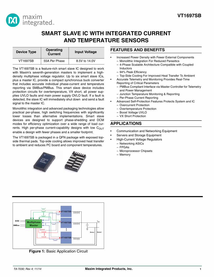
The VT1697SB is a feature-rich smart slave IC designed to workwith Maxim’s seventh-generation masters to implement a high-density multiphase voltage regulator. Up to six smart slave ICs,plus a master IC, provide a compact synchronous buck converterthat includes accurate individual phase-current and temperaturereporting via SMBus/PMBus. This smart slave device includesprotection circuits for overtemperature, VX short, all power sup-plies UVLO faults and main power supply OVLO fault. If a fault isdetected, the slave IC will immediately shut down and send a faultsignal to the master IC.
Monolithic integration and advanced packaging technologies allowpractical per-phase, high switching frequencies with significantlylower losses than alternative implementations. Smart slavedevices are designed to support phase-shedding and DCMmodes for efficiency optimization over a wide range of load cur-rents. High per-phase current-capability designs with low COUTenable a design with fewer phases and a smaller footprint.
The VT1697SB is packaged in a QFN package with exposed top-side thermal pads. Top-side cooling allows improved heat transferto ambient and reduces PC board and component temperatures.
Figure 1: Basic Application Circuit
FEATURES AND BENEFITS
• Increased Power Density with Fewer External Components– Monolithic Integration For Reduced Parasitics– 4-Phase Scalable Architecture Compatible with Coupled
Inductors– 94% Peak Efficiency– Top-Side Cooling For Improved Heat Transfer To Ambient
• Accurate Telemetry and Monitoring Provides Real-Time Reporting of Critical Parameters– PMBus Compliant Interface via Master Controller for Telemetry
and Power Management– Junction Temperature Monitoring & Reporting– Per-Phase Current Reporting
• Advanced Self-Protection Features Protects System and IC– Overcurrent Protection– Overtemperature Protection– Boost Voltage UVLO– VX Short Protection
APPLICATIONS
• Communication and Networking Equipment• Servers and Storage Equipment• High-Current Voltage Regulators
– Networking ASICs– FPGAs– Microprocessor Chipsets– Memory
Device TypeOperating
CurrentInput Voltage
VT1697SB 55A Per Phase 8.5V to 14.0V
Control1
ISENSE1
ISENSE2
ISENSE3
VOUT
Control2
Control6
Sense+ Sense-
TSENSE1
TSENSE2
TSENSE6
SVID
SMBusMultiphase
Master
VT1697SB
VT1697SB
VT1697SB

2 Maxim Integrated Products, Inc.
VT1697SB
Ordering Information
ABSOLUTE MAXIMUM RATINGS1
Supply Voltage (12V)........................................... -0.3V to 16V
Supply & Input Pin Voltages (1.8V) .................... -0.3V to 2.5V
Switching Node Voltage (VX) DC ........................ -0.3V to 16V
Switching Node Voltage (VX) 25ns2 ..................... -10V to 23V
VDDH Pin - VX Pin Differential 25ns4 .................... -10V to 23V
BST Pin (BST) DC............................................... -0.3V to 20V
BST Pin (BST) 25ns ............................................ -6.0V to 27V
BST Pin - VX Pin Differential ............................................2.5V
Operating Junction Temperature (TJ) ............................ 150°C
Storage Temperature Range ..........................-65°C to 150°C
Peak Reflow Temperature.............................................. 260°C
OPERATING RATINGS
VDD, VCC.......................................................... 1.71V to 1.98V
12V Supply (VDDH) ............................................ 8.5V to 14.0V
Junction Temperature (TJ) ............................... -40°C to 125°C
Frequency (Fsw).........................................300kHz to 1.3MHz
THERMAL RATINGS
VT1697SB JC Max .................................................0.42°C/W
Note 1: Stresses beyond those listed under “Absolute Maximum Ratings” may cause permanent damage to the device. These are stress ratings only;functional operation of the device at these or any other conditions beyond those indicated in the operational sections of the specifications is notimplied. Exposure to absolute maximum rating conditions for extended periods may affect device reliability.
Note 2: The 25ns rating is the allowable voltage that the VX node may exceed the -0.3V to 16V ratings in either positive or negative direction for up to 25ns per cycle.
Note 3: These products are completely Halogen-free and Pb-free, employing special materials sets: molding compounds/die attach materials and 100% matte tin plate including anneal. These products are RoHS compliant with an -e3 termination finish and are compatible with both SnPb and Pb-free soldering operations. These products are MSL classified at peak reflow temperatures that meet JEDEC JSTD-020.
Note 4: The VDDH input pin voltage AC should not exceed 19V (25ns). This measurement is taken at the VDDH pin referenced to VSS pin immediatelyadjacent using a high frequency scope probe with ILOAD at IMAX. A high-frequency input bypass capacitor must be located less than 60mils(1.524mm) from the VDDH pin and the Maxim device per our design guidelines.
Part Number Description Package Drawing Number Shipping Method Package Marking
RoHS Compliant3
VT1697SBFQX55A smart slave
DeviceQFN-16[Type G]
ES AP-2896 2.5ku Tape & Reel VT1697SBF
3 Maxim Integrated Products, Inc.
VT1697SB
Electrical Characteristics
VDD = VCC = 1.71V - 1.98V, VDDH = 12V. The symbol denotes specifications which apply over the following temperature range: TJ = 0 to 125°C, otherwise specifications are for TJ = 25°C. The # symbol denotes specifications which apply over the following temperature range: TJ = -25 to 125°C.
Symbol Parameter Conditions Min Typ Max UnitsSupply Voltages , Supply CurrentVDD, VCC Bias Supply Voltage 1.71 1.98 V
VDDH Power Train Input Voltage 8.5 12.0 14.0 V
ICC + IDD 1.8V Bias Supply Current
Shutdown (See Note 1) 0.5 2 µA
Inactive, No Switching (See Note 2) 3.2 5.0 mA
Load = 0A, VOUT = 1.8V, Fsw = 1.5MHz 43 61 mA
Load = 0A, VOUT = 1.8V, Fsw = 300KHz 14 20 mA
Load = 0A, VOUT = 1.8V, Fsw = 600KHz 29 41 mA
IDDH 12V Bias Supply CurrentShutdown (See Note 1) 1.3 10 µA
Inactive, No Switching (See Note 2) 6.5 20 µA
IRECON Specification
AI Current gain (IL to ISENSE) -70A < IL < 70A 95000 100000 105000 A/A
Temperature Sensor SpecificationsTRANGE Temperature Sensor Dynamic Range 0 150 °C
ATEMP Temperature Sensor Gain 3.01 mV/°C
– Temperature Sensor Voltage TJ = 0°C 832 mV
Protection Features
VDD_UVLO
VDD UVLO Threshold (Rising) 1.47 1.57 1.64 V
VDD UVLO Threshold (Falling) 1.41 1.5 1.58 V
VDDH_OVLO
VDDH OVLO Threshold (Rising) 15.48 16 16.41 V
VDDH OVLO Threshold (Falling) 14.95 15.5 15.81 V
VDDH_UVLO
VDDH UVLO Threshold (Rising) 4.05 4.27 4.40 V
VDDH UVLO Threshold (Falling) 3.90 4.09 4.25 V
VBST_UVLO
VBST UVLO Threshold (Rising) Note 3 1.39 1.52 1.66 V
VBST UVLO Threshold (Falling) Note 3 1.32 1.45 1.57 V
OCP
Peak Positive OCP Clamp Level 59 67 80 A
Peak Positive OCP Clamp Delay 63 ns
Peak Positive OCP Shutdown Level 99 110 121 A
Peak Positive OCP Shutdown Delay 42 ns
Peak Negative OCP Clamp Level -79.1 -71.9 -64.7 A
Peak Negative OCP Delay 110 ns
OTP Overtemperature Shutdown Rising Threshold 140 150 165 °C
PWM InputVIH Input Voltage, High State VDD - 0.20 V
VIL Input Voltage, Low State 0.20 V
– Tristate Control Threshold (VIN Rising) 0.63 V
TS_FAULTB InputVIH TS_FAULTB Digital Threshold VIH 0.41 V
VIL TS_FAULTB Digital Threshold VIL 0.17 V
Note 1: TSENSE, PWM and ISENSE pins of the slave are pulled LOW by the master. The slave is in this state before master OE is enabled.Note 2: Inactive, no switching: PWM signal is tristated by the master. The slave is in this mode when the master sheds a phase (temporarily disabling this slave) to save
power at lighter loads.Note 3: VBST_UVLO is measured with respect to VX and not from ground.
4 Maxim Integrated Products, Inc.
VT1697SB
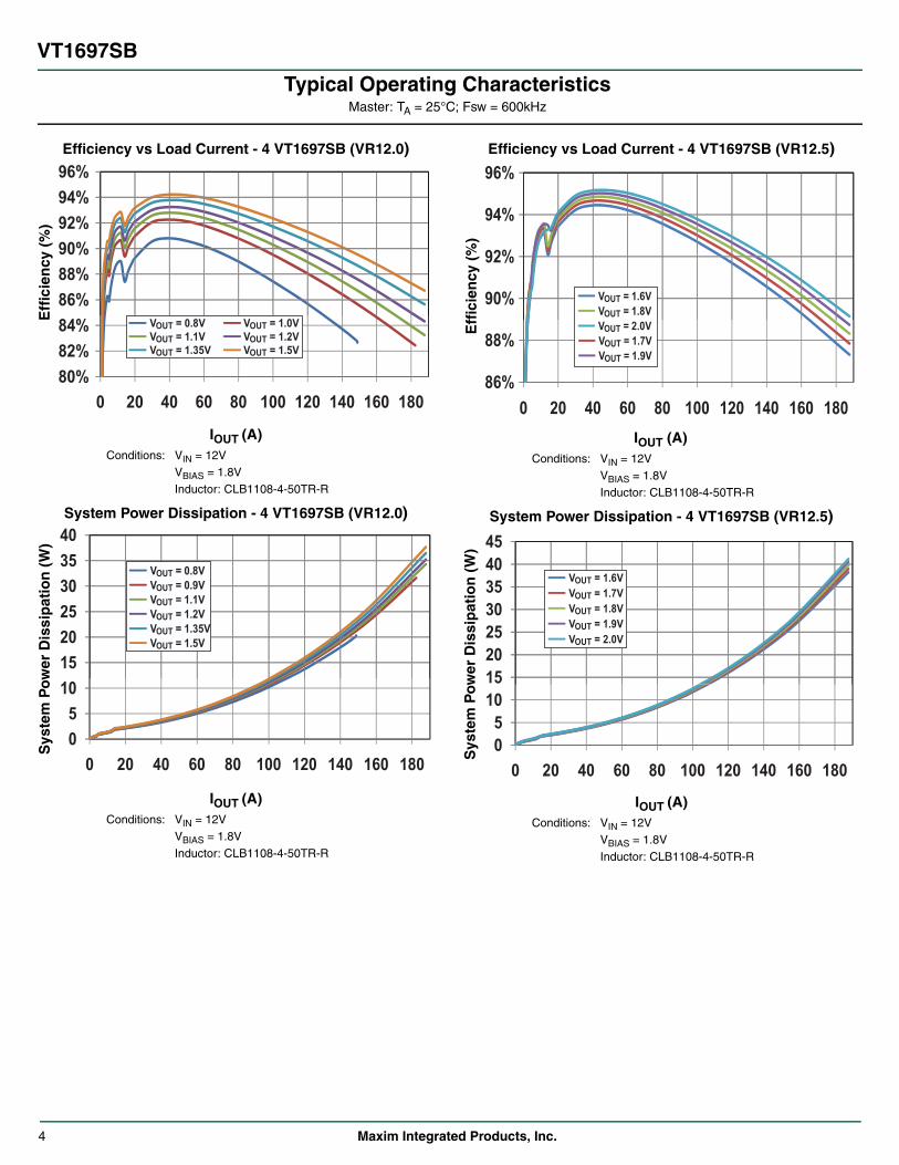
Typical Operating CharacteristicsMaster: TA = 25°C; Fsw = 600kHz
Efficiency vs Load Current - 4 VT1697SB (VR12.0)
IOUT (A)Conditions: VIN = 12V
VBIAS = 1.8VInductor: CLB1108-4-50TR-R
System Power Dissipation - 4 VT1697SB (VR12.0)
IOUT (A)Conditions: VIN = 12V
VBIAS = 1.8VInductor: CLB1108-4-50TR-R
Efficiency vs Load Current - 4 VT1697SB (VR12.5)
IOUT (A)Conditions: VIN = 12V
VBIAS = 1.8VInductor: CLB1108-4-50TR-R
System Power Dissipation - 4 VT1697SB (VR12.5)
IOUT (A)Conditions: VIN = 12V
VBIAS = 1.8VInductor: CLB1108-4-50TR-R
Eff
icie
ncy
(%
)
86%88%90%92%94%96%
80%82%84%
0 20 40 60 80 100 120 140 160 180
VOUT = 0.8V VOUT = 1.0VVOUT = 1.1V VOUT = 1.2VVOUT = 1.35V VOUT = 1.5V
Sys
tem
Po
wer
Dis
sip
atio
n (
W)
152025303540
05
10
0 20 40 60 80 100 120 140 160 180
VOUT = 0.8VVOUT = 0.9VVOUT = 1.1VVOUT = 1.2VVOUT = 1.35VVOUT = 1.5V
Eff
icie
ncy
(%
)
90%
92%
94%
96%
86%
88%
0 20 40 60 80 100 120 140 160 180
VOUT = 1.6VVOUT = 1.8V
VOUT = 1.7VVOUT = 1.9V
VOUT = 2.0V
Sys
tem
Po
wer
Dis
sip
atio
n (
W)
15202530354045
05
10
0 20 40 60 80 100 120 140 160 180
VOUT = 1.6VVOUT = 1.7VVOUT = 1.8VVOUT = 1.9VVOUT = 2.0V
5 Maxim Integrated Products, Inc.
VT1697SB
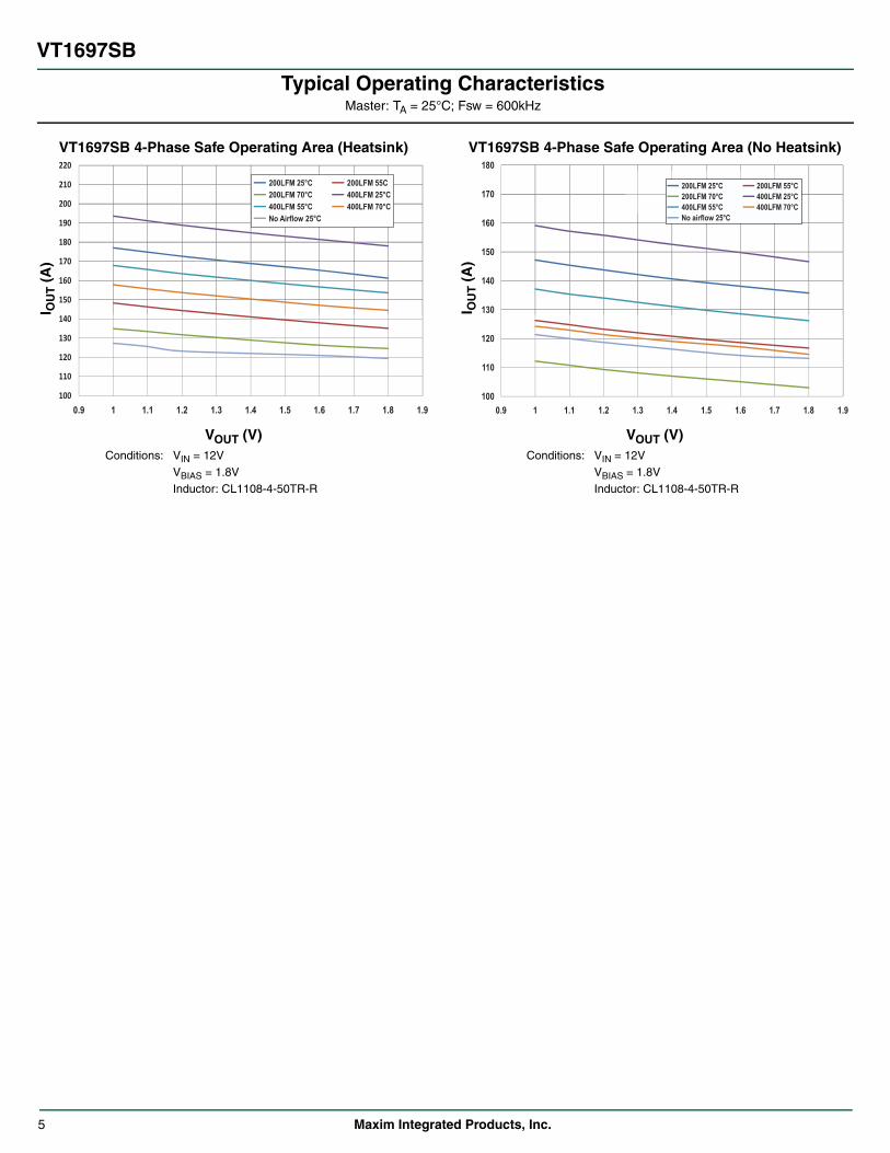
Typical Operating CharacteristicsMaster: TA = 25°C; Fsw = 600kHz
VT1697SB 4-Phase Safe Operating Area (Heatsink)
VOUT (V)Conditions: VIN = 12V
VBIAS = 1.8VInductor: CL1108-4-50TR-R
VT1697SB 4-Phase Safe Operating Area (No Heatsink)
VOUT (V)Conditions: VIN = 12V
VBIAS = 1.8VInductor: CL1108-4-50TR-R
I OU
T (
A)
150
160
170
180
190
200
210
220
100
110
120
130
140
0.9 1 1.1 1.2 1.3 1.4 1.5 1.6 1.7 1.8 1.9
200LFM 55C400LFM 25°C400LFM 70°C
200LFM 25°C200LFM 70°C400LFM 55°CNo Airflow 25°C
I OU
T (
A)
130
140
150
160
170
180
100
110
120
0.9 1 1.1 1.2 1.3 1.4 1.5 1.6 1.7 1.8 1.9
200LFM 25°C 200LFM 55°C200LFM 70°C 400LFM 25°C400LFM 55°C 400LFM 70°CNo airflow 25°C
6 Maxim Integrated Products, Inc.
VT1697SB
Pinout and Block Diagrams
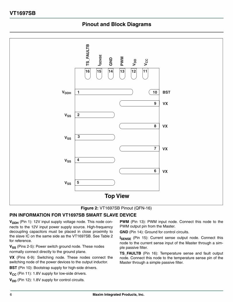
Figure 2: VT1697SB Pinout (QFN-16)
PIN INFORMATION FOR VT1697SB SMART SLAVE DEVICEVDDH (Pin 1): 12V input supply voltage node. This node con-nects to the 12V input power supply source. High-frequencydecoupling capacitors must be placed in close proximity tothe slave IC on the same side as the VT1697SB. See Table 2for reference.
VSS (Pins 2-5): Power switch ground node. These nodes normally connect directly to the ground plane.
VX (Pins 6-9): Switching node. These nodes connect theswitching node of the power devices to the output inductor.
BST (Pin 10): Bootstrap supply for high-side drivers.
VCC (Pin 11): 1.8V supply for low-side drivers.
VDD (Pin 12): 1.8V supply for control circuits.
PWM (Pin 13): PWM input node. Connect this node to thePWM output pin from the Master.
GND (Pin 14): Ground for control circuits.
ISENSE (Pin 15): Current sense output node. Connect thisnode to the current sense input of the Master through a sim-ple passive filter.
TS_FAULTB (Pin 16): Temperature sense and fault outputnode. Connect this node to the temperature sense pin of theMaster through a simple passive filter.
1
2
3
4
Top View
5
6
9
10
7
8
VDDH
VSS
VSS
VSS
VSS
16
TS
_FA
ULT
B
15
I SE
NS
E
14
GN
D
13
PW
M
12
VD
D
11
VC
C
BST
VX
VX
VX
VX
7 Maxim Integrated Products, Inc.
VT1697SB
Pinout and Block Diagrams
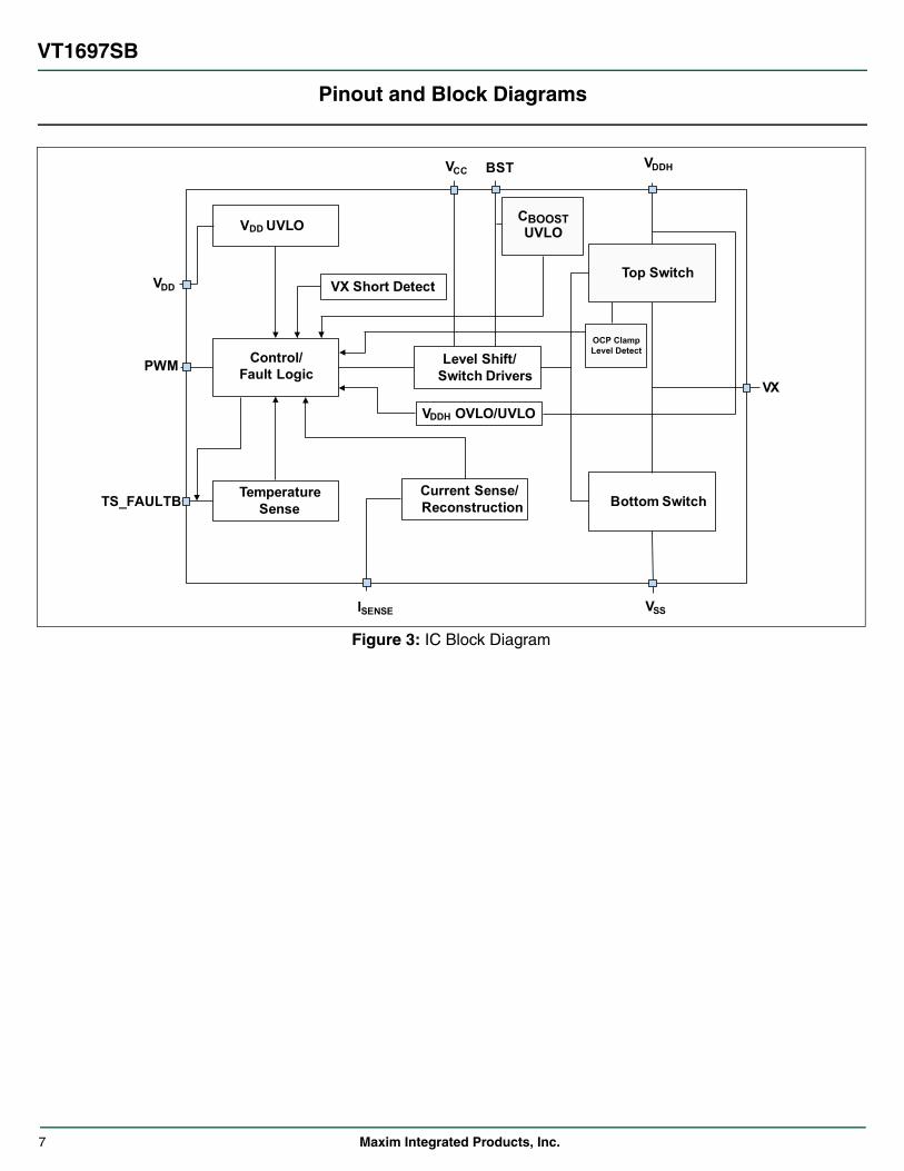
Figure 3: IC Block Diagram
Bottom Switch
Control/Fault Logic
Current Sense/ Reconstruction
Level Shift/ Switch Drivers
TemperatureSense
VDD UVLO
VX Short Detect
PWM
TS_FAULTB
VX
ISENSE
BSTVCC
VDD
VSS
VDDH
VDDH OVLO/UVLO
Top Switch
CBOOSTUVLO
OCP ClampLevel Detect
8 Maxim Integrated Products, Inc.
VT1697SB
Theory of Operation
VOLTAGE REGULATIONMaxim smart slave ICs provide the control logic, drivers, mon-itoring circuits and power semiconductors for a synchronousbuck converter with fault protection, status monitoring andaccurate lossless current sensing. Phases are controlled bythe Master IC independently by separate phase control sig-nals.Power Switch Control and Drivers The smart slave ICs operate in conjunction with a MaximMaster IC. The Master controller will configure the voltageregulator based on its configuration resistors and the numberof phases populated. The smart slave device’s switching iscontrolled by the proprietary command signals on the phasecontrol lines. The phase control signal has three definedstates: high, low and a "tri-state". "Tri-state" is used for phaseshedding and DCM modes. An external boost capacitor isrequired to supply the voltage for the high-side switch driver.VDD and VCC are brought out separately to allow separatedecoupling to improve noise immunity on the VDD rail. Current Sense OutputThe integrated lossless current sense (or “current reconstruc-tion”) produces a precise ratiometric current sense signal forboth positive and negative currents which is sent to the mas-ter as an analog current signal. This current sense technologyprovides accurate current information over load and tempera-ture that is not affected by tolerances of passive elementssuch as the output inductor, resistors and capacitors.Phase Configuration The ability for the Master to dynamically disable and re-enable a phase is an integral part of the Maxim Master/Slavearchitecture. The Master sets the phase control signal to “tri-state” to disable a phase. The same state is used to controlDCM operation. When using a coupled inductor, a proprietarymode (Coupled Inductor Mode) may be set by the master andcommunicated to the smart slave via the phase control signalto minimize losses due to coupled currents in inactive phases.
PROTECTION CIRCUITSOvercurrent Protection
The smart slave ICs incorporate instantaneous overcurrentfault protection using the lossless current sense/reconstruc-tion. This overcurrent protection is separate from the systemovercurrent protection, and is intended to operate only inextreme fault conditions to protect the IC and other compo-nents. The system overcurrent protection set by the mastershould be set with sufficient margin below the individualSlave’s threshold to ensure correct system operation.
For current sourcing operation, if the instantaneous current inthe top switch (based on the current sense/reconstruction cir-cuit) exceeds the overcurrent protection value shown in theElectrical Characteristics table, the slave will regulate theperiod of the top-side switch so as to keep its peak current ata safe level. The protection threshold has been set to ensure
that the IC's maximum allowable peak current is not exceededwhen using the recommended inductors. The sourcing cur-rent limiting is not considered a hard fault condition for slave,and therefore TS_FAULTB will not be asserted. Since clamp-ing is based on instantaneous reconstructed current, the rip-ple current must be considered when calculating themaximum average current per slave. The maximum averagecurrent before clamping can be calculated as shown inEquation 1. Note that the clamping is based on reconstructedcurrent. Limits shown in the Electrical Characteristics table forClamp Level reflect expected variations in application condi-tions and external component characteristics. Also note thatthe master (i.e., system) overcurrent protection should be setlower than the corresponding slaves' maximum operating cur-rent as stated above.
Equation 1
For current sinking protection, if the negative overcurrent pro-tection threshold is reached, the slave limits the current andTS_FAULTB is not asserted.
The VT1697SB implements an additional OCP shutdownlevel (beyond the clamp levels). If the current in the top switchexceeds the OCP shutdown level (shown in the ElectricalCharacteristics table), the IC is turned OFF and fault isreported by asserting FAULTB pin. The slave is then latchedOFF until the power is cycled.
VDD and VBOOST Undervoltage Lockout
The smart slave ICs include undervoltage lockout circuits:VDD and VBOOST. For power sequencing guidelines and oper-ation with separate bias rails for master and slaves, pleaserefer to appropriate master data sheet. VBOOST UVLO isactive at all times after the initial system start up. It is notactive during the initial system power on state (before regula-tion is enabled) and is activated approximately 20µs after ini-tial start up. If either of these UVLO circuits is tripped duringoperation, the smart slave will stop switching and a fault sig-nal (TS_FAULTB pulled LOW) will be sent to the master.
Maximum Average DC Slave Current OCPIRIPPLE
2-------------------–=
where,OCP = Peak OCP Clamp Level (A)IRIPPLE = Peak-to-Peak Inductor Ripple Current (A)
9 Maxim Integrated Products, Inc.
VT1697SB
Theory of Operation
VIN (VDDH) Undervoltage and Overvoltage Lockout
The slaves include protection circuits that shut down the slaveand assert TS_FAULTB if VDDH is above or below the correctoperating range. If either of these circuits is tripped duringoperation, the slave will stop switching and a fault signal(TS_FAULTB pulled LOW) will be sent to the master.
Temperature Sensing and Overtemperature Protection
Each smart slave IC incorporates an accurate die tempera-ture sensor. The temperature sense signal is sent to the mas-ter as an analog signal via the temperature sense pin. Theactual temperature of each smart slave device is then madeavailable via the SMBus of the master. The smart slave ICalso includes overtemperature protection. If the trip point isreached, the IC immediately shuts down and the fault isreported to the master via the TS_FAULTB pin.
VX Short Protection
The smart slave ICs include a VX short detection to detect alocal short circuit from the VX node to either VDDH or ground.If such a fault is detected, the slave shuts down and commu-nicates a fault to the master via the TS_FAULTB pin.
TS_FAULTB Signal
If a fault is detected, the smart slave sends a signal to themaster by pulling the TS_FAULTB pin to ground. Under nor-mal conditions, this pin is used to send an accurate analogrepresentation of the slave temperature. If a fault is detected,this pin is asserted LOW to indicate that a fault condition wasdetected by a slave IC. Table 1 shows the faults that result inthis signal being asserted. For a latching fault, the fault mustbe cleared and the VDD power cycled to re-enable the IC (fornon-latching faults, see note below the Table 1.). Please referto the applicable master IC data sheet for details about han-
Table 1: Fault Detection and Protection CircuitsFault Description Type Fault Flag (TS_FAULTB)
Boost UVLO Undervoltage Lockout on Boost Supply Shutdown* Asserted
VDDH UVLO Undervoltage Lockout on VDDH Shutdown* Asserted
VDDH OVLO Overvoltage Lockout Signal on VDDH Shutdown* Asserted
VDD UVLO Undervoltage Lockout Signal on VDD Shutdown* Asserted
VX Short VX Short-to-Ground or VDDH Shutdown Asserted
POCP (Sourcing) Positive/Sourcing Overcurrent Protection Cycle-by-Cycle Current Limit Not Asserted
NOCP (Sinking) Negative/Sinking Overcurrent Protection Cycle-by-Cycle Current Limit Not Asserted
OTP Overtemperature Protection Shutdown Asserted
* VDDH_UVLO, VDDH_OVLO, VBST_UVLO and VDD_UVLO are non-latching faults. If a non-latching fault is detected by the slave, it will assert TS_FAULTB signal low and stop switching. The slave resumes switching and de-asserts TS_FAULTB around 37µs from when the fault condition is removed. Please refer to the master data sheet for master response to TS_FAULTB asserted LOW by the slave device.
10 Maxim Integrated Products, Inc.
VT1697SB
Theory of Operation
DESIGN CONSIDERATIONSPhase Current Sharing and Steering Control
Maxim master/slave chipsets offer options for thermal balanc-ing in applications where one or more phases have differentthermal characteristics. The current sense and chipset regu-lation system offer the potential for current steering, where apercentage of current can be steered away from any phase,allowing that phase to operate at a different current than theother phases. This allows a precise scaling of current in anyslave(s) to achieve proper thermal balance between phases.Refer to the applicable Maxim master IC datasheet for moreinformation on how to program this feature.
Thermal Path and Printed Circuit Board Design
The smart slave IC has an exposed pad on the top-side of thepackage that is designed as an additional thermal path. Thispad is electrically connected to AGND/VSS, but is not intendedfor use as an electrical connection. Since there is normallysufficient airflow above the regulator, conducting heat fromthe top of the package results in a low junction-to-ambientthermal impedance, and hence lower junction temperature.This method provides additional thermal path to the heat flowfrom the die to the PCB to ambient and also reduces the tem-perature of the PCB. Thermal performance is presented forvarious thermal conditions and airflow rates in the SOA plots.
Printed Circuit Board (PCB) Layout
PCB layout can significantly affect the performance of the reg-ulator. Careful attention should be paid to the location of theinput capacitors and the output inductor which should beplaced close to the IC. The VX traces include large voltageswings (greater than 12V) with dv/dt greater than 10V/ns. It isrecommended that these traces are not only kept short, butalso are shielded with a ground plane immediately beneath.
Gerber files with layout information and complete referencedesigns can be obtained by contacting a Maxim account rep-resentative. Please contact Maxim to obtain QFN layoutguidelines for optimal design.
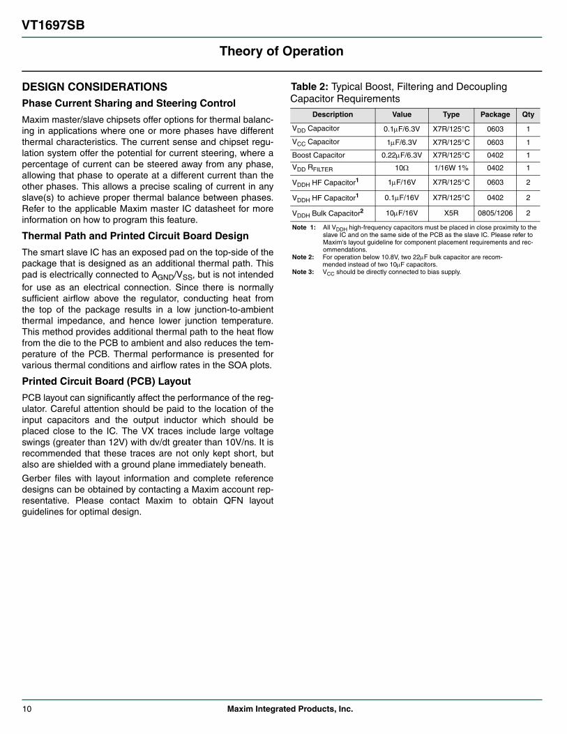
Table 2: Typical Boost, Filtering and Decoupling Capacitor Requirements
Description Value Type Package Qty
VDD Capacitor 0.1F/6.3V X7R/125°C 0603 1
VCC Capacitor 1F/6.3V X7R/125°C 0603 1
Boost Capacitor 0.22F/6.3V X7R/125°C 0402 1
VDD RFILTER 10 1/16W 1% 0402 1
VDDH HF Capacitor1 1F/16V X7R/125°C 0603 2
VDDH HF Capacitor1 0.1F/16V X7R/125°C 0402 2
VDDH Bulk Capacitor2 10F/16V X5R 0805/1206 2
Note 1: All VDDH high-frequency capacitors must be placed in close proximity to the slave IC and on the same side of the PCB as the slave IC. Please refer to Maxim's layout guideline for component placement requirements and rec-ommendations.
Note 2: For operation below 10.8V, two 22F bulk capacitor are recom-mended instead of two 10F capacitors.
Note 3: VCC should be directly connected to bias supply.
VT1697SB
11 Maxim Integrated Products, Inc.
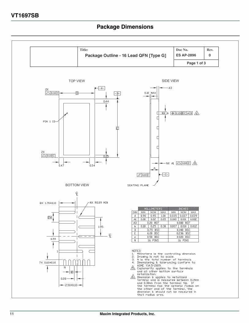
Package Dimensions
Package Outline - 16 Lead QFN [Type G]Title: Doc No. Rev.
ES AP-2896 0
Page 1 of 3
VT1697SB
12 Maxim Integrated Products, Inc.
Package Dimensions
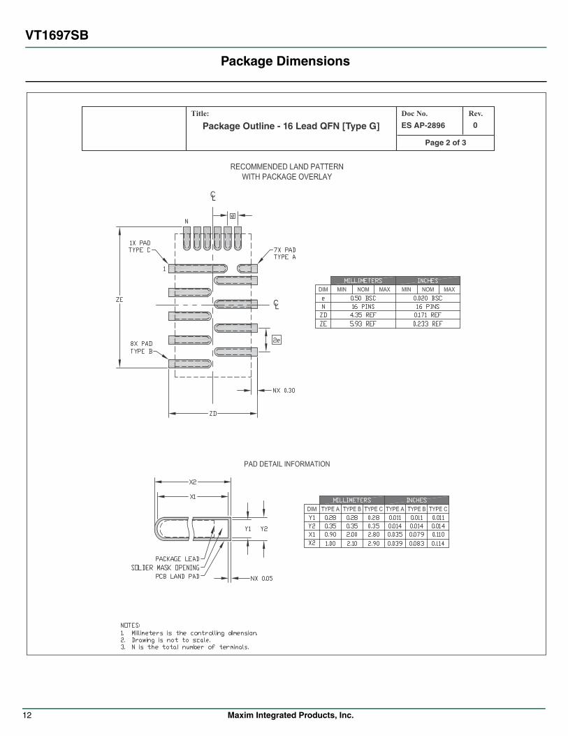
Title: Doc No. Rev.ES AP-2896 0
Page 2 of 3
Package Outline - 16 Lead QFN [Type G]
VT1697SB
13 Maxim Integrated Products, Inc.
Revision History
REVISION HISTORY
For pricing, delivery, and ordering information, please contact Maxim Direct at 1-888-629-4642, or visit Maxim Integrated’s website at www.maximintegrated.com.
Maxim Integrated cannot assume responsibility for use of any circuitry other than circuitry entirely embodied in a Maxim Inte-grated product. No circuit patent licenses are implied. Maxim Integrated reserves the right to change the circuitry and specifica-tions without notice at any time. The parametric values (min and max limits) shown in the Electrical Characteristics table areguaranteed. Other parametric values quoted in this data sheet are provided for guidance.
Maxim Integrated and the Maxim Integrated logo are trade-marks of Maxim Integrated Products, Inc. © 2014 Maxim Integrated Products, Inc.
Revision Description Date
0 Initial Data Sheet N/A
1
Changed Status of VT1697SB to New Product.Updated ICC + IDD, VBST_UVLO and NOCP specifications in the Electrical Characteristics table.
Made a change in the “filter” (from VDDH to VDD) in Table 2.1/14
2 Updated to Maxim Template 2/14
3Updated Electrical Characteristics Table and Overcurrent Protection section.Updated Operating Current Rating to 55A.Removed all VT1677SB references from data sheet.
9/14
4 Removed “Scalable 120A Multiphase Solution in < 835mm2” in Features and Benefits section 11/14