slus940c –september 2009–revised december … · – available in small 2-mm × 2-mm or the end...
TRANSCRIPT

Battery Pack
VBUS
GND
D+
D-
USB Port
DC
1 Fm1 Fm1kW
1.5kW
2kW
+
GND
Adaptor
VDD
D-
D+
GND
TTDM
Host
System Load
Disconnect after Detection
OR
ISET/100/500 mA
1
2
3
4
5
10
9
8
7
6
IN
ISET
VSS
PRETERM
D+ D-
ISET2
CHG
TS
OUT
bq24050/2
+
Product
Folder
Sample &Buy
Technical
Documents
Tools &
Software
Support &Community
ReferenceDesign
bq24050, bq24052, bq24055SLUS940C –SEPTEMBER 2009–REVISED DECEMBER 2014
bq2405x 1-A, Single-Cell Li-Ion and Li-Pol Battery Charger With Automatic Adaptorand USB Detection
1 Features 3 DescriptionThe bq2405x series of devices are highly integrated
1• ChargingLi-Ion and Li-Pol linear chargers devices targeted at– 1% Charge Voltage Accuracy space-limited portable applications. The devices
– 10% Charge Current Accuracy operate from either a USB port or AC adapter. Thehigh-input voltage range with input overvoltage– Pin Selectable USB 100-mA and 500-mAprotection supports low-cost unregulated adapters.Maximum Input Current LimitThe bq2405x has a single power output that charges– Programmable Termination and Prechargethe battery. A system load can be placed in parallelThresholdwith the battery as long as the average system load• Protection does not keep the battery from charging fully during
– 30-V Input Rating; With 6.6-V Input the 10-hour safety timer.Overvoltage Protection
The battery is charged in three phases: conditioning,– Input Voltage Dynamic Power Management constant current, and constant voltage. In all charge– 125 °C Thermal Regulation; 150°C Thermal phases, an internal control loop monitors the IC
junction temperature and reduces the charge currentShutdown Protectionif an internal temperature threshold is exceeded.– OUT Short-Circuit Protection and ISET Short
Detection The charger power stage and charge current sensefunctions are fully integrated. The charger function– Operation Over JEITA Range Through Batteryhas high accuracy current and voltage regulationNTC - ½ Fast-Charge-Current at Cold, 4.06 Vloops, charge status display, and charge termination.at HotThe precharge current and termination current
– Fixed 10-Hour Safety Timer threshold are programmed through an external• System resistor. The fast charge current value is also
programmable through an external resistor.– Auto Input Source Detection (D+, D– Pins)– No Device Transceiver Required Device Information(1)
– USB Friendly PART NUMBER PACKAGE BODY SIZE (NOM)– Automatic Termination and Timer Disable bq24050
WSON (10) 2.00 mm × 2.00 mmMode (TTDM) for Absent Battery Pack With bq24052Thermistor bq24055 WSON (12) 2.00 mm × 3.00 mm
– Status Indication – Charging/Done(1) For all available packages, see the orderable addendum at
– Available in Small 2-mm × 2-mm or the end of the datasheet.2-mm × 3-mm Package
Simplified Circuit2 Applications• Smart Phones• PDAs• MP3 Players• Low-Power Handheld Devices
1
An IMPORTANT NOTICE at the end of this data sheet addresses availability, warranty, changes, use in safety-critical applications,intellectual property matters and other important disclaimers. PRODUCTION DATA.

bq24050, bq24052, bq24055SLUS940C –SEPTEMBER 2009–REVISED DECEMBER 2014 www.ti.com
Table of Contents7.4 Device Functional Modes........................................ 251 Features .................................................................. 17.5 Programming........................................................... 252 Applications ........................................................... 1
8 Application and Implementation ........................ 263 Description ............................................................. 18.1 Application Information............................................ 264 Revision History..................................................... 28.2 Typical Applications ................................................ 265 Pin Configuration and Functions ......................... 3
9 Power Supply Recommendations ...................... 306 Specifications......................................................... 410 Layout................................................................... 316.1 Absolute Maximum Ratings ..................................... 4
10.1 Layout Guidelines ................................................. 316.2 Handling Ratings ...................................................... 410.2 Layout Example .................................................... 316.3 Recommended Operating Conditions ...................... 410.3 Thermal Considerations ........................................ 326.4 Thermal Information .................................................. 5
11 Device and Documentation Support ................. 336.5 Electrical Characteristics........................................... 511.1 Documentation Support ........................................ 336.6 Timing Requirements ................................................ 911.2 Related Links ........................................................ 336.7 Switching Characteristics .......................................... 911.3 Trademarks ........................................................... 336.8 Typical Characteristics ............................................ 1011.4 Electrostatic Discharge Caution............................ 337 Detailed Description ............................................ 1411.5 Glossary ................................................................ 337.1 Overview ................................................................. 14
12 Mechanical, Packaging, and Orderable7.2 Functional Block Diagram ....................................... 15Information ........................................................... 337.3 Feature Description................................................. 16
4 Revision HistoryNOTE: Page numbers for previous revisions may differ from page numbers in the current version.
Changes from Revision B (June 2012) to Revision C Page
• Added Handling Rating table, Feature Description section, Device Functional Modes, Application andImplementation section, Power Supply Recommendations section, Layout section, Device and DocumentationSupport section, and Mechanical, Packaging, and Orderable Information section................................................................ 1
Changes from Revision A (September 2009) to Revision B Page
• Changed all occurrences of Li-Ion To: Li-Ion and Li-Pol ........................................................................................................ 1
Changes from Original (August 2009) to Revision A Page
• Changed the status of the devices From: Product Preview To: Production Data .................................................................. 1
2 Submit Documentation Feedback Copyright © 2009–2014, Texas Instruments Incorporated
Product Folder Links: bq24050 bq24052 bq24055

1
2
3
4
5
12
11
10
9
8
IN
PRETERM
ISET
VSS
D+ D-
ISET2
CHG
TS
OUT
6 7PG NC
1
2
3
4
5
10
9
8
7
6
IN
ISET
VSS
PRETERM
D+ D-
ISET2
CHG
TS
OUT
bq24050, bq24052, bq24055www.ti.com SLUS940C –SEPTEMBER 2009–REVISED DECEMBER 2014
5 Pin Configuration and Functions
DSQ PackageDSS Package10-Pin WSON With Exposed Thermal Pad
12-Pin WSON With Exposed Thermal Padbq24050/bq24052 Top Viewbq24055 Top View
NOTE: NC - No internal connection
Pin FunctionsPIN I/O DESCRIPTION
NAME NO.bq24050/2 bq24055
Low (FET on) indicates charging and Open Drain (FET off) indicates no Charging orCHG 8 10 O Charge complete.D+ 5 5 I USB port D+ input connectionD– 6 8 I USB port D– input connection
Input power, connected to external DC supply (AC adapter or USB port). Expected rangeIN 1 1 I of bypass capacitors 1 μF to 10 μF, connect from IN to VSS.Programs the Fast-charge current setting. External resistor from ISET to VSS defines fastISET 2 2 I charge current value. Range is 52.3k (10 mA) to 540 Ω (1.0 A).Programming the Input/Output Current Limit for the USB or Adaptor source: High = 500
ISET2 7 9 I mA max, Low = ISET, FLOAT = 100 mA max. D+D– Detection initially sets the chargethreshold and requires ISET2 to change states to take control.
NC – 7 NA Do not make connection to this pin (internal use) – Do not route through this pinBattery Connection. System Load may be connected. Average load should not be
OUT 10 12 O excessive, allowing battery to charge within the 10-hour safety timer window. Expectedrange of bypass capacitors 1 μF to 10 μF.Low (FET on) indicates the input voltage is above UVLO and the OUT (battery) voltagePG – 6 O and less than VOVP
Programs the Current Termination Threshold (5 to 50% of Iout which is set by ISET) andSets the Precharge Current to twice the Termination Current Level.
PRE-TERM 4 4 IExpected range of programming resistor is 1k to 10 kΩ (2k: IOUT/10 for term; IOUT/5 forprecharge)Temperature sense pin connected to ‘50/55 –10k at 25C NTC thermistor, ’52 – 100k NTCat 25°C, in the battery pack. Floating TS Pin or pulling High puts part in TTDM and disableTS monitoring, Timers and Termination. Pulling pin Low disables the IC (CE function). IfTS 9 (1) 11 I NTC sensing is not needed, connect this pin to VSS through an external ‘50/55-10-kΩ/’52-100-kΩ resistor. A ‘50/55-250-kΩ/’52-880-kΩ from TS to ground will prevent ICentering TTDM when battery with thermistor is removed.
VSS 3 3 – Ground terminal
(1) Spins have different pin definitions
Copyright © 2009–2014, Texas Instruments Incorporated Submit Documentation Feedback 3
Product Folder Links: bq24050 bq24052 bq24055

bq24050, bq24052, bq24055SLUS940C –SEPTEMBER 2009–REVISED DECEMBER 2014 www.ti.com
Pin Functions (continued)PIN I/O DESCRIPTION
NAME NO.bq24050/2 bq24055
There is an internal electrical connection between the exposed thermal pad and the VSSThermal Pad pin of the device. The thermal pad must be connected to the same potential as the VSSPad and Pad 2x2mm2 –2x3mm2 pin on the printed circuit board. Do not use the thermal pad as the primary ground inputPackage for the device. VSS pin must be connected to ground at all times.
6 Specifications
6.1 Absolute Maximum Ratings (1)
over operating free-air temperature range (unless otherwise noted)MIN MAX UNIT
Input Voltage IN (with respect to VSS) –0.3 30 VOUT (with respect to VSS) –0.3 7 VPRE-TERM, ISET, ISET2, TS, CHG, PG, D+, D–, –0.3 7 V(with respect to VSS)
Input Current IN 1.25 AOutput Current (Continuous) OUT 1.25 AOutput Sink Current CHG 15 mAJunction temperature, TJ –40 150 °C
(1) Stresses beyond those listed under Absolute Maximum Ratings may cause permanent damage to the device. These are stress ratingsonly, and functional operation of the device at these or any other conditions beyond those indicated under Recommended OperatingConditions is not implied. Exposure to absolute-maximum-rated conditions for extended periods may affect device reliability. All voltagevalues are with respect to the network ground terminal unless otherwise noted.
6.2 Handling RatingsMIN MAX UNIT
Tstg Storage temperature range –65 150 °CHuman body model (HBM), per ANSI/ESDA/JEDEC JS-001, all 3000pins (1)
V(ESD) Electrostatic discharge VCharged device model (CDM), per JEDEC specification 1500JESD22-C101, all pins (2)
(1) JEDEC document JEP155 states that 500-V HBM allows safe manufacturing with a standard ESD control process.(2) JEDEC document JEP157 states that 250-V CDM allows safe manufacturing with a standard ESD control process.
6.3 Recommended Operating Conditions (1)
MIN NOM UNITIN voltage range 3.5 28 V
VIN IN operating voltage range, Restricted by VDPM and VOVP 4.45 6.45 VIIN Input current, IN pin 1.0 AIOUT Current, OUT pin 1.0 ATJ Junction temperature 0 125 °CRPRE-TERM Programs precharge and termination current thresholds 1 10 kΩRISET Fast-charge current programming resistor 0.540 52.3 kΩ
10k NTC thermistor range without entering TTDM, bq24050/55 1.66 258 kΩRTS 100k NTC thermistor range without entering TTDM, bq24052 24 885 kΩ
(1) Operation with VIN less than 4.5 V or in drop-out may result in reduced performance.
4 Submit Documentation Feedback Copyright © 2009–2014, Texas Instruments Incorporated
Product Folder Links: bq24050 bq24052 bq24055

bq24050, bq24052, bq24055www.ti.com SLUS940C –SEPTEMBER 2009–REVISED DECEMBER 2014
6.4 Thermal Informationbq24050 bq24055bq24052
THERMAL METRIC (1) UNITDSQ DSS10 PINS 12 PINS
RθJA Junction-to-ambient thermal resistance 63.5 61.8RθJC(top) Junction-to-case (top) thermal resistance 79.5 70.9RθJB Junction-to-board thermal resistance 33.9 25.7
°C/WψJT Junction-to-top characterization parameter 7.8 1.9ψJB Junction-to-board characterization parameter 34.3 25.7RθJC(bot) Junction-to-case (bottom) thermal resistance 7.5 7.2
(1) For more information about traditional and new thermal metrics, see the IC Package Thermal Metrics application report, SPRA953.
6.5 Electrical CharacteristicsOver junction temperature range 0°C ≤ TJ ≤ 125°C and recommended supply voltage (unless otherwise noted)
PARAMETER TEST CONDITIONS MIN TYP MAX UNIT
INPUT
UVLO Undervoltage lock-out Exit VIN: 0V → 4V Update based on sim/char 3.15 3.3 3.45 V
VIN: 4V→0V,VHYS_UVLO Hysteresis on VUVLO_RISE falling 175 230 280 mVVUVLO_FALL = VUVLO_RISE –VHYS-UVLO
Input power good detection threshold (Input power good if VIN > VOUT + VIN-DT); VOUT =VIN-DT 30 80 145 mVis VOUT + VIN-DT 3.6V, VIN: 3.5V → 4V
VHYS-INDT Hysteresis on VIN-DT falling VOUT = 3.6V, VIN: 4V → 3.5V 31 mV
VOVP Input overvoltage protection threshold VIN: 5V → 7V (50/52/55) 6.5 6.65 6.8 V
VHYS-OVP Hysteresis on OVP VIN: 11V → 5V 95 mV
Feature active in USB mode; Limit Input Source 4.34 4.4 4.46Current to 50mA; VOUT=3.5V; RISET = 825ΩUSB/Adaptor low input voltageVIN-DPM VFeature active in Adaptor mode; Limit Inputprotection. Restricts lout at VIN-DPM
Source Current to 50mA; VOUT=3.5V; RISET = 4.24 4.3 4.36825Ω
USB input I-Limit 100 mA ISET2 = Float; RISET = 825Ω 85 92 100IIN-USB-CL mA
USB input I-Limit 500 mA ISET2 = High; RISET = 825Ω 430 462 500
ISET SHORT CIRCUIT TEST
Highest Resistor value considered a Riset: 600Ω → 250Ω, Iout latches off. CycleRISET_SHORT 280 500 Ωfault (short). Monitored for Iout>90mA power to Reset. USB100 mode.
Maximum OUT current limit VIN = 5V, VOUT = 3.6V, VISET2 =Low, Riset: 600ΩIOUT_CL 1.05 1.4 ARegulation (Clamp) → 250Ω, Iout latches off after tDGL-SHORT
BATTERY SHORT PROTECTION
OUT pin short-circuit detectionVOUT(SC) VOUT:3V → 0.5V, no deglitch 0.75 0.8 0.85 Vthreshold/ precharge threshold
Recovery ≥ VOUT(SC) + VOUT(SC-HYS); Rising, noVOUT(SC-HYS) OUT pin Short hysteresis 77 mVDeglitch
Source current to OUT pin duringIOUT(SC) 10 15 20 mAshort-circuit detection
QUIESCENT CURRENT
IOUT(PDWN) Battery current into OUT pin VIN = 0V 1μA
IOUT(DONE) OUT pin current, charging terminated VIN = 6V, VOUT > VOUT(REG) 6
IIN(STDBY) Standby current into IN pin TS = LO, VIN ≤ 6V 125 μA
TS = open, VIN = 6V, TTDM – no load on OUTICC Active supply current, IN pin 0.8 1 mApin, VOUT > VOUT(REG), IC enabled
BATTERY CHARGER FAST-CHARGE
VOUT(REG) Battery regulation voltage VIN =5.5V, IOUT =25mA, VTS-45°C≤ VTS ≤ VTS-0°C 4.16 4.20 4.23 V
VO_HT(REG) Battery hot regulation Voltage VIN =5.5V, IOUT =25mA, VTS-60°C≤ VTS ≤ VTS-45°C 4.02 4.06 4.1 V
Programmed Output “fast charge” VOUT(REG) > VOUT > VLOWV, VIN = 5V, ISET2=Lo,IOUT(RANGE) 10 800 mAcurrent range RISET = 675 to 10.8kΩ
Copyright © 2009–2014, Texas Instruments Incorporated Submit Documentation Feedback 5
Product Folder Links: bq24050 bq24052 bq24055

bq24050, bq24052, bq24055SLUS940C –SEPTEMBER 2009–REVISED DECEMBER 2014 www.ti.com
Electrical Characteristics (continued)Over junction temperature range 0°C ≤ TJ ≤ 125°C and recommended supply voltage (unless otherwise noted)
PARAMETER TEST CONDITIONS MIN TYP MAX UNIT
Adjust VIN down until IOUT = 0.5A, VOUT = 4.15V,VDO(IN-OUT) Drop-Out, VIN – VOUT RISET = 675 , ISET2=Lo (Adaptor Mode); Tj ≤ 325 500 mV
100°C
IOUT Output “fast charge” formula VOUT(REG) > VOUT > VLOWV, VIN = 5V, ISET2=Lo KISET/RISET A
RISET = KISET /IOUT 50 < IOUT < 1.0 A 510 540 570
KISET Fast charge current factor RISET = KISET /IOUT 25 < IOUT < 50 mA 480 527 600 AΩ
RISET = KISET /IOUT 10 < IOUT < 25 mA 350 520 680
PRECHARGE – SET BY PRETERM PIN
Precharge to fast-charge transitionVLOWV 2.4 2.5 2.6 Vthreshold
Deglitch time on precharge to fast-tDGL1(LOWV) 70 μscharge transition
IPRE-TERM Refer to the Termination Section
Precharge Current Level, Default VOUT < VLOWV; RPRE-TERM = High Z (≥13kΩ); RISET 18 20 22 %IOUT-CCSetting = 1k%PRECHG
Precharge current formula RPRE-TERM = KPRE-CHG (Ω/%) × %PRE-CHG (%) RPRE-TERM/KPRE-CHG
VOUT < VLOWV, VIN = 5V, RPRE-TERM = 2k to 10kΩ;RISET = 1080Ω , RPRE-TERM = KPRE-CHG × %IFAST- 90 100 110 Ω/%CHG, where %IFAST-CHG is 20 to 100%
KPRE-CHG % Precharge FactorVOUT < VLOWV, VIN = 5V, RPRE-TERM = 1k to 2kΩ;RISET = 1080Ω, RPRE-TERM = KPRE-CHG × %IFAST- 84 100 117 Ω/%CHG, where %IFAST-CHG is 10% to 20%
TERMINATION – SET BY PRE-TERM PIN
Termination Current Threshold, VOUT > VRCH; RPRE-TERM = High Z (≥13kΩ); RISET 9 10 11 %IOUT-CCDefault Setting = 1k%TERM
Termination Current Threshold RPRE-TERM = KTERM (Ω/%) × %TERM (%) RPRE-TERM/ KTERMFormula
VOUT > VRCH, VIN = 5V, RPRE-TERM = 2k to 10kΩ ;RISET = 750Ω; KTERM × %IFAST-CHG, where %IFAST- 182 200 216CHG is 10 to 50%
KTERM % Term Factor Ω/%VOUT > VRCH, VIN = 5V, RPRE-TERM = 1k to 2kΩ ;RISET = 750Ω; KTERM × %IFAST-CHG, where %IFAST- 174 199 224CHG is 5 to 10%
Current for programming the term.IPRE-TERM and precharge with resistor. ITerm-Start RPRE-TERM = 2k, VOUT = 4.15V 71 75 81 μA
is the initial PRE-TERM curent.
%TERM Termination current formula RTERM/ KTERM
Elevated PRE-TERM current for, tTerm-ITerm-Start Start, during start of charge to prevent 80 85 92 μA
recharge of full battery,
RECHARGE OR REFRESH
Recharge detection threshold – VO(REG)–0. VO(REG) VO(REG)–0.VIN = 5V, VTS = 0.5V, VOUT: 4.25V → VRCH VNormal Temp 120 –0.095 070VRCH
Recharge detection threshold – Hot VO_HT(REG) VO_HT(REG) VO_HT(REG)VIN = 5V, VTS = 0.2V, VOUT: 4.15V → VRCH VTemp –0.130 –0.105 –0.080
BATTERY DETECT ROUTINE (1)
VOUT Reduced regulation during VO(REG)–0. VO(REG–0. VO(REG)–0.VREG-BD Vbattery detect 450 400 350VIN = 5V, VTS = 0.5V, Battery AbsentIBD-SINK Sink current during VREG-BD 7 10 mA
VO(REG)–0. VO(REG)–0. VO(REG)–0.VBD-HI High battery detection threshold VIN = 5V, VTS = 0.5V, Battery Absent V150 100 050
VREG-BD VREG-BD VREG-BDVBD-LO Low battery detection threshold VIN = 5V, VTS = 0.5V, Battery Absent V+0.050 +0.100 +0.150
BATTERY-PACK NTC MONITOR (2)
NTC bias current; 10k NTCINTC-10k VTS = 0.3V 48 50 52 μAthermsistor, bq24050/5
(1) In Hot Mode VO(REG) becomes VO_HT(REG)(2) TS pin: bq24050/5: 10k NTC; bq24052: 100k NTC; See the TS Section for Thermistor Information
6 Submit Documentation Feedback Copyright © 2009–2014, Texas Instruments Incorporated
Product Folder Links: bq24050 bq24052 bq24055

bq24050, bq24052, bq24055www.ti.com SLUS940C –SEPTEMBER 2009–REVISED DECEMBER 2014
Electrical Characteristics (continued)Over junction temperature range 0°C ≤ TJ ≤ 125°C and recommended supply voltage (unless otherwise noted)
PARAMETER TEST CONDITIONS MIN TYP MAX UNIT
NTC bias current; 100k NTCINTC-100k VTS = 0.3V 4.8 5 5.2 μAthermsistor, bq24052
bq24050/5 bias current whenINTC-DIS-10k VTS = 0V 27 30 34 μACharging is disabled.
bq24052 bias current when ChargingINTC-DIS-100k VTS = 0V 4.4 5 5.8 μAis disabled.
INTC is reduced prior to enteringINTC-FLDBK-10k TTDM to keep cold thermistor from VTS: Set to 1.525V 4 5 6.5 μA
entering TTDM, bq24050/5
INTC is reduced prior to enteringINTC-FLDBK-100k TTDM to keep cold thermistor from VTS: Set to 1.525V 1.1 1.5 1.9 μA
entering TTDM, bq24052
Termination and timer disable modeVTTDM(TS) VTS: 0.5V → 1.7V; Timer Held in Reset 1550 1600 1650 mVThreshold – Enter
VHYS-TTDM(TS) Hysteresis exiting TTDM VTS: 1.7V → 0.5V; Timer Enabled 100 mV
VCLAMP(TS) TS maximum voltage clamp VTS= Open (Float) 1800 1950 2000 mV
INTC adjustment (90 to 10%; 45 to 6.6uA) takesTS voltage where INTC is reduce toVTS_I-FLDBK place near this spec threshold. 1475 mVkeep thermistor from entering TTDM VTS: 1.425V → 1.525V
CTS Optional Capacitance – ESD 0.22 μF
bq2405x Low temperature CHG Low Temp Charging to Pending;VTS-0°C 1205 1230 1255 mVPending VTS: 1V → 1.5V
Charge pending to low temp charging; VTS: 1.5VVHYS-0°C Hysteresis at 0°C 86 mV→ 1V
Normal charging to low temp charging; VTS: 0.5VVTS-10°C Low temperature, half charge 765 790 815 mV→ 1V
Low temp charging to normal CHG;VHYS-10°C Hysteresis at 10°C 35 mVVTS: 1V → 0.5V
Normal charging to high temp CHG;VTS-45°C High temperature at 4.1V 263 278 293 mVVTS: 0.5V → 0.2V
High temp charging to normal CHG;VHYS-45°C Hysteresis at 45°C 10.7 mVVTS: 0.2V → 0.5V
High temp charge to pending;VTS-60°C High temperature Disable 170 178 186 mVVTS: 0.2V → 0.1V
Charge pending to high temp CHG;VHYS-60°C Hysteresis at 60°C 11.5 mVVTS: 0.1V → 0.2V
VTS-EN-10k Charge Enable Threshold, (10k NTC) VTS: 0V → 0.175V; 80 88 96 mV
HYS below VTS-EN-10k to Disable, (10kVTS-DIS_HYS-10k VTS: 0.125V → 0V; 12 mVNTC)
Charge Enable Threshold, (100kVTS-EN-100k VTS: 0V → 0.175V 140 150 160 mVNTC)
HYS below VTS-EN-100k to Disable,VTS-DIS_HYS-100k VTS: 0.125V → 0V; 50 mV(100k NTC)
THERMAL REGULATION
TJ(REG) Temperature regulation limit 125 °C
TJ(OFF) Thermal shutdown temperature 155 °C
TJ(OFF-HYS) Thermal shutdown hysteresis 20 °C
LOGIC LEVELS ON ISET2
VIL Logic LOW input voltage Sink more than 8μA 0.4 V
VIH Logic HIGH input voltage Source more than 8μA 1.4 V
IIL Sink current required for LO 2 9 μA
IIH Source current required for HI 1.1 8 μA
VFLT ISET2 Float Voltage 650 900 1200 mV
D+/D– DETECTION – bq2405x
VD+ Bias at D+, during detection routine Can source at least 200μA 0.475 0.6 0.7 V
Current Limit at D+ pin, duringID+ VD+ = 0V 1.5 mAdetection routine
Copyright © 2009–2014, Texas Instruments Incorporated Submit Documentation Feedback 7
Product Folder Links: bq24050 bq24052 bq24055

bq24050, bq24052, bq24055SLUS940C –SEPTEMBER 2009–REVISED DECEMBER 2014 www.ti.com
Electrical Characteristics (continued)Over junction temperature range 0°C ≤ TJ ≤ 125°C and recommended supply voltage (unless otherwise noted)
PARAMETER TEST CONDITIONS MIN TYP MAX UNIT
Current Sink at D– pin, duringID– VD– = 0.5V 50 100 150 μAdetection routine
D+ leakage when not in detectionID+_LEAK VD+ = 5V 1 μAmode
D– leakage when not in detectionID–_LEAK VD– = 5V 1 μAmode
VDPDM_0.4V D– Comparator Threshold Rising 0.35 0.45 V
VDPDM_HYS_0.4V D– Comparator Hysteresis 42 mV
VDPDM_0.8V D+/D– Comparator Threshold Rising 0.75 0.875 V
VDPDM_HYS_0.8V D+/D– Comparator Hysteresis 42 mV
LOGIC LEVELS ON CHG AND PG
VOL Output LOW voltage ISINK = 5mA 0.4 V
Ilkg Leakage current into IC V CHG = 5V, V PG = 5V 1 μA
8 Submit Documentation Feedback Copyright © 2009–2014, Texas Instruments Incorporated
Product Folder Links: bq24050 bq24052 bq24055

bq24050, bq24052, bq24055www.ti.com SLUS940C –SEPTEMBER 2009–REVISED DECEMBER 2014
6.6 Timing RequirementsMIN NOM MAX UNIT
PRECHARGE – SET BY PRETERM PINtDGL2(LOWV) Deglitch time on fast-charge to precharge transition 32 msTERMINATION – SET BY PRE-TERM PINtDGL(TERM) Deglitch time, termination detected 29 mstTerm-Start Elevated termination threshold initially active for tTerm-Start 1.25 minBATTERY-PACK NTC MONITOR (1)
tDGL(TTDM) Deglitch exit TTDM between states 57 msDeglitch enter TTDM between states 8 μs
(1) TS pin: bq24050/5: 10k NTC; bq24052: 100k NTC; See the TS Section for Thermistor Information
6.7 Switching Characteristicsover operating free-air temperature range (unless otherwise noted)
PARAMETER TEST CONDITIONS MIN TYP MAX UNIT
INPUT
Time measured from VIN: 0V → 5V 1μs rise-tDGL(PG_PWR) Deglitch time on exiting sleep. 45 μstime to PG = low, VOUT = 3.6V
Deglitch time on VHYS-INDT power down. Time measured from VIN: 5V → 3.2V 1μs fall-tDGL(PG_NO-PWR) 29 msSame as entering sleep. time to PG = High Z, VOUT = 3.6V
tDGL(OVP-SET) Input overvoltage blanking time VIN: 5V → 12V 113 μs
Time measured from VIN: 12V → 5V 1μs fall-tDGL(OVP-REC) Deglitch time exiting OVP 30 μstime to PG = LO
ISET SHORT CIRCUIT TEST
Deglitch time transition from ISET shorttDGL_SHORT Clear fault by cycling IN or TS 1 msto Iout disable
RECHARGE OR REFRESH
Deglitch time, recharge threshold VIN = 5V, VTS = 0.5V, VOUT: 4.25V → 3.5V intDGL1(RCH) 29 msdetected 1μs; tDGL1(RCH) is time to ISET ramp
Deglitch time, recharge threshold VIN = 5V, VTS = 0.5V, VOUT = 3.5V inserted;tDGL2(RCH) 3.6 msdetected in OUT-Detect Mode tDGL2(RCH) is time to ISET ramp
BATTERY DETECT ROUTINE (1)
tDGL(HI/LOW REG) Regulation time at VREG or VREG-BD VIN = 5V, VTS = 0.5V, Battery Absent 25 ms
BATTERY CHARGING TIMERS AND FAULT TIMERS
Restarts when entering precharge; AlwaystPRECHG Precharge safety timer value 1700 1940 2250 senabled when in precharge.
Clears fault or resets at UVLO, TS (CE)tMAXCH Charge safety timer value 34000 38800 45000 sdisable, OUT Short, exiting LOWV and Refresh
BATTERY-PACK NTC MONITOR (2)
Normal to Cold Operation: VTS: 0.6V → 1V 40 mstDGL(TS_10C) Deglitch for TS thresholds: 10°C
Cold to Normal Operation: VTS: 1.0V → 0.6V 12 ms
tDGL(TS) Deglitch for TS thresholds: 0/45/60C. Battery charging 30 ms
D+/D– DETECTION – bq2405x
DetectionTime from start of D+/D– t = 0 at D– pulled-up > 0.5V or D+ pulled uptDPDM 65 msdetection to latched output externally, >0.8V
(1) In Hot Mode VO(REG) becomes VO_HT(REG)(2) TS pin: bq24050/5: 10k NTC; bq24052: 100k NTC; See the TS Section for Thermistor Information
Copyright © 2009–2014, Texas Instruments Incorporated Submit Documentation Feedback 9
Product Folder Links: bq24050 bq24052 bq24055

Vin
Viset
Vchg
Vpg
t - time - 100ms/div
2V/div
2V/div
2V/div
5V/div
Vin
Viset
Vchg
Vpg
t - time - 20ms/div
2V/div
2V/div
5V/div
2V/div
Vin
D+
Vd-
Viset
Vchg
End ofDetectionRoutine
Detection RoutineStarted
USB CommunicationBetween Host andDevice Receiver
t - time - 50ms/div
2V/div
5V/div
2V/div
1V/div
1V/div
Vin
D+
Vd-
Viset
Vchg
t - time - 100ms/div
2V/div
2V/div
5V/div
1V/div
1V/div
Vin
D+
Vd-
Viset
Vchg
t - time - 100ms/div
2V/div
2V/div
5V/div
1V/div
1V/div
D+
Vd-
Viset
Vchg
t - time - 10ms/div
2V/div
2V/div
2V/div
1V/div
1V/div
Vin
bq24050, bq24052, bq24055SLUS940C –SEPTEMBER 2009–REVISED DECEMBER 2014 www.ti.com
6.8 Typical CharacteristicsSETUP: bq24055 typical applications schematic; VIN = 5 V, VBAT = 3.6 V (unless otherwise indicated)RISET = 1k; IOUT_FAST_CHG = 540 mA; RPAC_TERM = 2k; IOUT_PRE_CHG = 108 mA; IOUT_TERM = 54 mA
6.8.1 Power Up, Down, OVP, Disable and Enable Waveforms
. .Detected D– line pulled to 0.6 V and the detection routine is No signal detected on D+ or D–. After 500 ms, the detectionstarted routine is forced to run
Figure 1. D+ D– Detection for Adaptor Hot Plug Figure 2. D+ D– Detection for Unknown Source Hot Plug
(Device transceiver is "dead") After 500 ms, the detection routineis forced to run.
Figure 4. D+ D– Detection for USB Hot Plug With PullupFigure 3. D+ D– Detection for USB Hot Plug No Pullup
VIN = 0 V → 5 V → 8 V → 5 V
Figure 5. OVP 8-V Adaptor – Hot Plug Figure 6. OVP from Normal Operation
10 Submit Documentation Feedback Copyright © 2009–2014, Texas Instruments Incorporated
Product Folder Links: bq24050 bq24052 bq24055

Viset
Vchg
V_0.1 _OUTW
Vout
Battery Declared Absent
t - time - 20ms/div
100mV/div
1V/div
1V/div
5V/div
Viset
Vchg
Vts
Vout 1 Battery Detect Cycle
Entered TTDM
t - time - 10ms/div
5V/div
1V/div
1V/div
1V/div
Vin
Viset
Vts
Vout
t - time - 5ms/div
2V/div
2V/div
1V/div
500mV/div
bq24050, bq24052, bq24055www.ti.com SLUS940C –SEPTEMBER 2009–REVISED DECEMBER 2014
Power Up, Down, OVP, Disable and Enable Waveforms (continued)
42-Ω Load 100–Ω Load
Figure 7. Battery Removal – GND Removed First Figure 8. Battery Removal With OUT andTS Disconnect First
.Continuous battery detection when not in TTDM
Figure 9. Battery Removal With Fixed TS = 0.5 V
Copyright © 2009–2014, Texas Instruments Incorporated Submit Documentation Feedback 11
Product Folder Links: bq24050 bq24052 bq24055

528
530
532
534
536
538
540
542
544
546
0 0.2 0.4 0.6 0.8
I - Output Current - AO
Kiset
K-
iset
W
.15
Low to High Currents(may occur in recharge to fast charge transion)
High to Low Currents(may occur in Voltage Regulation - Taper Current)
Vin
Viset
Vchg
Vpg
t - time - 20ms/div
5V/div
5V/div
1V/div
1V/div
Vin
Viset
Vchg
V_0.1 _OUTW
t - time - 500 s/divm
2V/div
2V/div
500mV/div
20mV/div
Viset
VoutVin
V_0.1 _OUTW
ExitsThermal
Regulation
EntersThermalRegulation
t - time - 1s/div
2V/div
1V/div
1V/div
50mV/div
Vin
Viset
Vchg
V_0.1 _OUTW
Short Detected in 100mAmode and Latched Off
t - time - 5ms/div
2V/div
2V/div
500mV/div
20mV/div
Vin
Viset
Vchg
V_0.1 _OUTW
t - time - 1ms/div
2V/div
2V/div
20mV/div
500mV/div
bq24050, bq24052, bq24055SLUS940C –SEPTEMBER 2009–REVISED DECEMBER 2014 www.ti.com
6.8.2 Protection Circuits Waveforms
CH4: IOUT (0.2A/Div) CH4: IOUT (0.2A/Div)
Figure 10. ISET Shorted Before USB Power Up Figure 11. DPM – Adaptor Current Limits –VIN Regulated to 4.3 V
The IC temperature rises to 125°C and enters thermalregulation. Charge current is reduced to regulate the IC at 125°C.VIN is reduced, the IC temperature drops, the charge currentreturns to the programmed value.
Figure 13. Thermal Regulator – VIN IncreasesFigure 12. DPM – USB Current Limits– VIN Regulated to 4.4 V
VIN swept from 5 V to 3.9 V to 5 V, VBAT = 4 V
Figure 14. Entering and Exiting Sleep Mode Figure 15. KISET for Low and High Currents
12 Submit Documentation Feedback Copyright © 2009–2014, Texas Instruments Incorporated
Product Folder Links: bq24050 bq24052 bq24055
361.8
362
362.2
362.4
362.6
362.8
363
363.2
363.4
2.5 3 3.5 4 4.5
V - Output Voltage - VO
I-
Ou
tpu
t C
urr
en
t -
mA
O
I @ 0°CO
I @ 25°CO
I @ 85°CO
4.196
4.198
4.2
4.202
4.204
4.206
4.208
4.21
4.212
4.5 5 5.5 6 6.5
R 100OUT = Ω
V @ 25°CO
V @ 85°CO
V - Input Voltage DC - VI
V-
Ou
tpu
t V
olt
ag
e D
C -
VO
UT
V @ 0°CO
4.192
4.193
4.194
4.195
4.196
4.197
4.198
4.199
4.2
0 0.2 0.4 0.6 0.8 1
I - Output Current - AO
V-
Ou
tpu
t V
olt
ag
e -
VO
V @ 25°Creg
V @ 85°Creg
V @ 0°Creg
bq24050, bq24052, bq24055www.ti.com SLUS940C –SEPTEMBER 2009–REVISED DECEMBER 2014
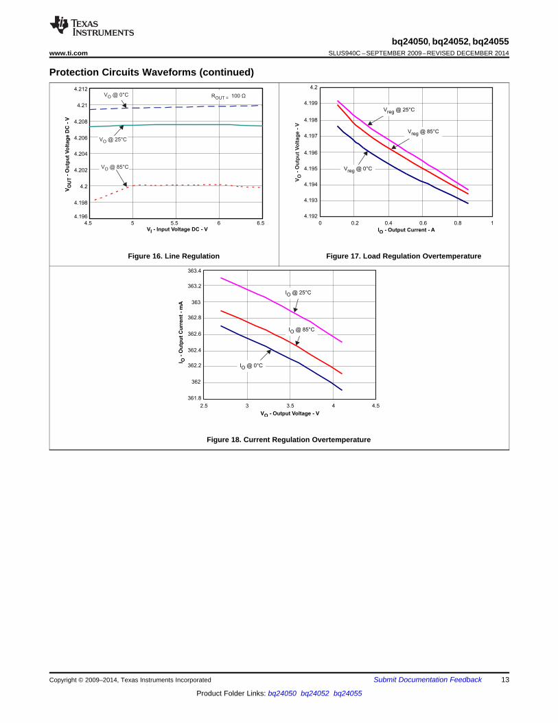
Protection Circuits Waveforms (continued)
Figure 16. Line Regulation Figure 17. Load Regulation Overtemperature
Figure 18. Current Regulation Overtemperature
Copyright © 2009–2014, Texas Instruments Incorporated Submit Documentation Feedback 13
Product Folder Links: bq24050 bq24052 bq24055

bq24050, bq24052, bq24055SLUS940C –SEPTEMBER 2009–REVISED DECEMBER 2014 www.ti.com
7 Detailed Description
7.1 OverviewThe bq2405x is a highly integrated family of 2-mm × 2-mm or 2-mm × 3-mm single-cell Li-Ion and Li-Polchargers. The charger can be used to charge a battery, power a system or both. The charger has three phasesof charging: precharge to recover a fully discharged battery, fast-charge constant current to supply the buckcharge safely and voltage regulation to safely reach full capacity. The charger is flexible, allowing programmingof the fast-charge current, precharge current and termination. This charger is designed to work with a USBconnection or adaptor (DC out). The charger also checks to see if a battery is present.
The charger also comes with a full set of safety features: JEITA Temperature Standard, Overvoltage Protection,DPM-IN, Safety Timers, and ISET short protection. All of these features and more are described in detail below.
The charger is designed for a single power path from the input to the output to charge a single cell Li-Ion orLi-Pol battery pack. Upon application of a 5VDC power source the D+, D– detection routine is run to determine ifthe source is an Adaptor or a USB port. This feature is useful, when the battery is discharged (USB transceiverdead) or there is no transceiver, by early detection of an adaptor, thus allowing initial charging at the adaptorlevel. ISET and OUT short checks are performed in parallel with the detection routine to assure a proper chargecycle.
If the battery voltage is below the LOWV threshold, the battery is considered discharged and a preconditioningcycle begins. The amount of precharge current can be programmed using the PRE-TERM pin which programs apercent of fast charge current (10 to 100%) as the precharge current. This feature is useful when the system loadis connected across the battery stealing the battery current. The precharge current can be set higher to accountfor the system loading while allowing the battery to be properly conditioned. The PRE-TERM pin is a dual-function pin which sets the precharge current level and the termination threshold level. The termination "currentthreshold" is always half of the precharge programmed current level.
Once the battery voltage has charged to the VLOWV threshold, fast charge is initiated and the fast charge currentis applied. The fast charge constant current is programmed using the ISET pin. The constant current provides thebulk of the charge. Power dissipation in the IC is greatest in fast charge with a lower battery voltage. If the ICreaches 125°C, the IC enters thermal regulation. Slow the timer clock by half and reduce the charge current asneeded to keep the temperature from rising any further. Figure 19 shows the charging profile with thermalregulation. Typically under normal operating conditions, the IC’s junction temperature is less than 125°C andthermal regulation is not entered.
Once the cell has charged to the regulation voltage the voltage loop takes control and holds the battery at theregulation voltage until the current tapers to the termination threshold. The charge termination can be disabled ifdesired. The CHG pin is low (LED on) during the first charge cycle only and turns off once the charge terminationthreshold is reached, regardless if termination is enabled or disabled.
The TS pin monitors the voltage across the pack thermistor and implements the JEITA standard. This allows forreduced voltage regulation at hot temperatures and reduced charge currents at low temperatures. The TS pinincorporates a chip disable feature when pulled low and an Termination and Timer Disable Mode (TTDM) featurewhen left floating or pulled high.
14 Submit Documentation Feedback Copyright © 2009–2014, Texas Instruments Incorporated
Product Folder Links: bq24050 bq24052 bq24055

Charge
Pump
IN OUT
OUTREGREF
T CJo
TJ°C
125
Thermal Regulation
°CREF
IN
IN
ISET
Charge
Pump
PRE-TERM
75 Am+
CHARGE
CONTROL
OUT
VTERM_EN
ISET2 (LOW = ISET, HI = USB500,
FLOAT = USB100)
VCOLD-FLT
VHOT-45C
VTTDMTS
5 Am 45 Am
VCLAMP = 1.4 V
Cold Temperature
Sink Current
= 45 Am
LO = TTDM MODE
HI = CHIP DISABLE
OUT
CHG
ON:
On During1st Charge Only
OFF:
+Increased from 75 A to 85 A form m
1st
minute of charge.
+_ +
_
+_
+_
+_
+_
+_
+_
+_
+_
+_
+_
Internal Charge
Current Sense
w/Multiple Outputs
+_
USB Sense
Resistor USB100/500REF
+_
1.5 V
FAST CHARGE
PRE-CHARGE
PG
HI = Suspend CHG
VCOLD-10C
VHOT-FLT
+_
+_
HI = Half CHG (JEITA)
HI = 4.06Vreg (JEITA)
VDISABLE
D+ / D-
DETECTION
CONTROL
- On Initial
Supply Power
Connection
D+
D-
0.6 V(200 mA)
(100 mA)
bq24055 Only
+
-
80
mV
OUT
Input
Power
I x 1.5 V
540 A
OUT
W
+_
IN-DPMREF
150 C
Thermal Shutdown
o
REF
0.9 V Float
+_
Disable
Sink Current
= 20 Am
X2 Gain (1:2)
Term:Pre-CHG
Term Reference
Pre-CHG Reference
Detect
IN
+_
OVPREF
bq24050, bq24052, bq24055www.ti.com SLUS940C –SEPTEMBER 2009–REVISED DECEMBER 2014
7.2 Functional Block Diagram
Copyright © 2009–2014, Texas Instruments Incorporated Submit Documentation Feedback 15
Product Folder Links: bq24050 bq24052 bq24055

PRE-CHARGECURRENT ANDTERMINATIONTHRESHOLD
FAST-CHARGECURRENT
T(PRECHG)
ChargeComplete
Status,Charger
Off
Pre-Conditioning
Phase
CurrentRegulation
Phase
Voltage Regulation andCharge Termination
Phase
BatteryVoltage,V(OUT)
Battery Current,I(OUT)
DONE
0A
ThermalRegulation
Phase
Temperature, Tj
IO(OUT)
T(THREG)
I(TERM)IO(PRECHG)
VO(REG)
VO(LOWV)
DONET(CHG)
bq24050, bq24052, bq24055SLUS940C –SEPTEMBER 2009–REVISED DECEMBER 2014 www.ti.com
Functional Block Diagram (continued)
Figure 19. Charging Profile With Thermal Regulation
7.3 Feature Description
7.3.1 Power Down, or Undervoltage Lockout (UVLO):The bq2405x family is in power down mode if the voltage of the IN pin is less than UVLO. The part is considereddead and all the pins are high impedance. Once the IN voltage rises above the UVLO threshold the IC entersSleep Mode or Active mode depending on the voltage of the OUT pin (battery).
7.3.2 Power UpThe IC is alive after the IN voltage ramps above UVLO (see Sleep Mode), resets all logic and timers, and startsto perform the D+D– detection along with many of the continuous monitoring routines. The D+/D– detectiontypically take less than 100 ms, but can take as long as 600 ms if there is no activity on the D+ or D– lines whichindicates the device transceiver nor an adaptor is present. Typically the input voltage quickly rises through theUVLO and sleep states where the IC declares power good, starts the qualification charge at 100 mA, finishes theUSB detection routine, sets the input current limit threshold base on the source detected (ISET=adaptor or100mA=USB), starts the safety timer, and enables the CHG pin. See Figure 21.
7.3.3 D+, D– Detection:This detection is designed to give the charger advance notice that an adaptor or USB port is connect for thecases where the battery is discharged and device transceiver is not able to communicate with a USB host orthere is not a device transceiver. If an adaptor is detected, then the charger can immediately start charging at theprogrammed ISET level. Without this early detection, the charger would have to default to the 100-mA inputcurrent level to make sure it was not over-loading a low power USB port. The detection method monitors the D+,D– communication lines looking for a short between the lines (Adaptor source connected) or pulldown resistorson D+, D– (USB source connected) to determine what source is connected (no USB communication takesplace). If an adaptor source is detected then the charger will transition from the 100 mA startup level to the ISETprogrammed current level. If a USB port is detected, the input current limit will stay at the 100 mA level. If adifferent charge level is desired, than the one detected, the host has to change the state of the ISET2 pin(signals the internal logic to start using the ISET2 as the program pin) and then set to the desired state.
16 Submit Documentation Feedback Copyright © 2009–2014, Texas Instruments Incorporated
Product Folder Links: bq24050 bq24052 bq24055
bq24050, bq24052, bq24055www.ti.com SLUS940C –SEPTEMBER 2009–REVISED DECEMBER 2014
Feature Description (continued)The D+ and D– pin connections inside the charger are disconnected within 100 ms of the D+ or D– lines beingpulled high (start of detection), to minimize any interaction between the charger detection pins and the USBnormal communications. If the device transceiver is able to communicate with the USB host, communicationtypically starts after 100 ms after the device has pulled the D+ or D– line high indicating it is “on line”, and bythen the IC detection is complete and has been disconnected. The device host then may change the ISET2 levelor disable the IC by pulling the TS pin low.
7.3.4 New Charge CycleA new charge cycle is started when a good power source is applied, performing a chip disable/enable (TS pin),exiting Termination and Timer Disable Mode (TTDM), detecting a battery insertion or the OUT voltage droppingbelow the VRCH threshold. The CHG pin is active low only during the first charge cycle, therefore exiting TTDMor a dropping below VRCH will not turn on the CHG pin FET, if the CHG pin is already high impedance.
Copyright © 2009–2014, Texas Instruments Incorporated Submit Documentation Feedback 17
Product Folder Links: bq24050 bq24052 bq24055

LD
O
VS
S
1.8
V
0V
LD
OH
YS
0°C
0°C
HY
S
10°C
10°C
HY
S
45°C
45°C
HY
S
60°C
60°C
HY
S
EN
DIS
HY
S
t DG
L(T
S)
t DG
L(T
S)
t DG
L(T
S)
t DG
L(T
S)
t DG
L(T
S_IO
C)
Ris
ing
t DG
L(T
S_IO
C)
Falli
ng
t DG
L(T
S)
t DG
L(T
S)
t DG
L(T
TD
M)
Exit
t DG
L(T
TD
M)
Ente
r
t <
tD
GL(T
TD
M)
Exit
t <
tD
GL(I
S)
Norm
al
Opera
tion
LD
OM
ode
Norm
al
Opera
tion
Cold
Opera
tion
Cold
Fault
LD
OM
ode
Cold
Fault
Norm
al
Opera
tion
t DG
L(T
S)
t DG
L(T
TD
M)
Ente
r
Dis
able
dC
old
Opera
tion
HO
TF
ault
4.0
6 V
HO
TO
pera
tion
Norm
al
Opera
tion
4.0
6 V
HO
TO
pera
tion
Dis
able
d
t DG
L(T
S1_IO
C)
Cold
to N
orm
al
Dra
win
g N
ot to
Scale
Dots
Show
Thre
shold
Trip P
oin
tsfllo
wed b
y a
deglit
ch tim
e b
efo
retr
ansitio
nin
g into
a n
ew
mode.
t
bq24050, bq24052, bq24055SLUS940C –SEPTEMBER 2009–REVISED DECEMBER 2014 www.ti.com
Feature Description (continued)
Figure 20. TS Battery Temperature Bias Threshold and Deglitch Timers
18 Submit Documentation Feedback Copyright © 2009–2014, Texas Instruments Incorporated
Product Folder Links: bq24050 bq24052 bq24055

Apply Input
Power
Turn on PG FET – PG pin LOW
Set Input Current Limit to 100mA
and Start Charge
Perform ISET & OUT short tests
Remember ISET2 State
Has ISET2 changed state since
Detection Routine was run?
Yes
Set charge current
based on ISET2 truth
table.
Return to
Charge
No
Yes
Is Chip Enabled &Alive?
VTS > VEN
& VIN>VUVLO
No
Yes
Is power good?
VBAT+VDT < VIN < VOVP
& VUVLO < VIN
No
Yes
Set charge current
based Detection
Routine..
Start Running USB
Detection Routine
bq24050, bq24052, bq24055www.ti.com SLUS940C –SEPTEMBER 2009–REVISED DECEMBER 2014
Feature Description (continued)
Figure 21. Power Up Flow Diagram
7.3.5 Overvoltage Protection (OVP) – Continuously MonitoredIf the input source applies an overvoltage, the pass FET, if previously on, turns off after a deglitch, tBLK(OVP). Thetimer ends and the CHG and PG pin goes to a high impedance state. Once the overvoltage returns to a normalvoltage, the PG pin goes low, timer continues, charge continues and the CHG pin goes low after a 25-msdeglitch. PG pin is optional on some packages.
Copyright © 2009–2014, Texas Instruments Incorporated Submit Documentation Feedback 19
Product Folder Links: bq24050 bq24052 bq24055

bq24050, bq24052, bq24055SLUS940C –SEPTEMBER 2009–REVISED DECEMBER 2014 www.ti.com
Feature Description (continued)7.3.6 Power Good Indication (PG)After application of a 5 V source, the input voltage rises above the UVLO and sleep thresholds (VIN> VOUT+VDT),but is less than OVP (VIN< VOVP), then the PG FET turns on and provides a low impedance path to ground. SeeFigure 5, Figure 6, and Figure 14.
7.3.7 CHG Pin IndicationThe charge pin has an internal open drain FET which is on (pulls down to VSS) during the first charge only(independent of TTDM) and is turned off once the battery reaches voltage regulation and the charge currenttapers to the termination threshold set by the PRE-TERM resistor.
The charge pin will be high impedance in sleep mode and OVP (if PG is high impedance) and return to itsprevious state when the condition is removed.
Cycling input power, pulling the TS pin low and releasing or entering precharge mode will cause the CHG pin toreset and is considered the start of a first charge.
7.3.8 CHG and PG LED Pullup SourceFor host monitoring, a pullup resistor is used between the STATUS pin and the VCC of the host and for a visualindication a resistor in series with an LED is connected between the STATUS pin and a power source. If theCHG or PG source can exceed 7 V, a 6.2-V Zener diode should be used to clamp the voltage. If the source isthe OUT pin, note that as the battery changes voltage, the brightness of the LEDs vary.
CHARGING STATE CHG FET/LED1st Charge ON
Refresh ChargeOVP OFF
SLEEPTEMP FAULT ON for 1st Charge
VIN POWER GOOD STATE PG FET/LEDUVLO
SLEEP Mode OFFOVP Mode
Normal Input (VOUT + VDT < VIN < ONVOUP)PG is independent of chip disable (bq24055, VTS = 0V)
7.3.9 Input DPM Mode (VIN-DPM or IN-DPM)The IN-DPM feature is used to detect an input source voltage that is folding back (voltage dropping), reaching itscurrent limit due to an excessive load. When the input voltage drops to the VIN-DPM threshold the internal passFET starts to reduce the current until there is no further drop in voltage at the input. This would prevent a sourcewith voltage less than VIN-DPM to power the out pin. This works well with current limited adaptors and USB portsas long as the nominal voltage is above 4.3 V and 4.4 V respectively. This is an added safety feature that helpsprotect the source from excessive loads.
7.3.10 OUTThe OUT pin of the charger provides current to the battery and to the system, if present. This IC can be used tocharge the battery plus power the system, charge just the battery or just power the system (TTDM) assuming theloads do not exceed the available current. The OUT pin is a current limited source and is inherently protectedagainst shorts. If the system load ever exceeds the output programmed current threshold, the output will bedischarged unless there is sufficient capacitance or a charged battery present to supplement the excessive load.
20 Submit Documentation Feedback Copyright © 2009–2014, Texas Instruments Incorporated
Product Folder Links: bq24050 bq24052 bq24055

0
0.2
0.4
0.6
0.8
1
1.2
1.4
1.6
1.8
100 1000 10000
I -SET W
I-
Ou
tpu
t C
urr
en
t -
AO
I Internal Clamp RangeOUT
I Short
FaultRange
SET
Non RestrictedOperating Area
I ProgrammedOUT
min
max
IC
lam
p m
in -
max
OU
T
IF
ault m
in -
max
OU
T
0
0.5
1
1.5
2
2.5
3
3.5
4
4.5
0.6 1.8
V - Voltage - VTS
No
rmalized
OU
T C
urr
en
t an
d V
- V
RE
G 60 C to 45 CHOT TEMP
4.06VRegulation
o o
IOUT
VOUT
0 0.2 0.4 0.8 1 1.2 1.4 1.6
For < 45 C, 4.2V Regulationo
H
ot F
ault
No OperationDuring Cold
Fault
ColdFault
IC D
isable
0 Co
< 48 Co
60 Co
10 Co
100% of ProgrammedCurrent
50%
Term
ination
Dis
able
bq24050, bq24052, bq24055www.ti.com SLUS940C –SEPTEMBER 2009–REVISED DECEMBER 2014
7.3.11 ISETAn external resistor is used to Program the Output Current (10 mA to 1.0 A) and can be used as a currentmonitor.RISET = KISET ÷ IOUT (1)
Where:IOUT is the desired fast charge current;KISET is a gain factor found in the electrical specification
For greater accuracy at lower currents, part of the sense FET is disabled to give better resolution. Figure 15shows the transition from low current to higher current. Going from higher currents to low currents, there ishysteresis and the transition occurs around 0.15 A.
The ISET resistor is short protected and will detect a resistance lower than ≉340 Ω. The detection requires atleast 80 mA of output current. If a “short” is detected, then the IC will latch off and can only be reset by cyclingthe power. The OUT current is internally clamped to a maximum current between 1.05 A and 1.4 A and isindependent of the ISET short detection circuitry, as shown in Figure 23. Also, see Figure 30 and Figure 10.
Figure 22. Operation Over TS Bias Voltage Figure 23. Programmed / Clamped Out Current
Copyright © 2009–2014, Texas Instruments Incorporated Submit Documentation Feedback 21
Product Folder Links: bq24050 bq24052 bq24055

bq24050, bq24052, bq24055SLUS940C –SEPTEMBER 2009–REVISED DECEMBER 2014 www.ti.com
7.3.12 TSThe TS pin is designed to follow the new JEITA temperature standard for Li-Ion and Li-Pol batteries. There arenow four thresholds, 60°C, 45°C, 10°C, and 0°C. Normal operation occurs from 10°C to 45°C. If between 0°Cand 10°C the charge current level is cut in half and if between 45°C and 60°C the regulation voltage is reducedto 4.1 Vmax, see Figure 22. The TS feature is implemented using an internal 50-μA current source to bias thethermistor (bq24050/5 designed for use with a 10k NTC β = 3370 (SEMITEC 103AT-2 or Mitsubishi TH05-3H103F), and bq24052 with a 100k NTC β = 3540 (Mitsubishi TH05-36104F) or equivalent) connected from theTS pin to VSS. If this feature is not needed, a fixed 10k can be placed between TS and VSS to allow normaloperation. This may be done if the host is monitoring the thermistor and then the host would determine when topull the TS pin low to disable charge.
The TS pin has two additional features, when the TS pin is pulled low or floated/driven high. A low disablescharge (similar to a CE feature) and a high puts the charger in TTDM.
Above 60°C or below 0°C the charge is disable. Once the thermistor reaches ≉–10°C the TS current folds backto keep a cold thermistor (from –10°C to –50°C) from placing the IC in the TTDM mode. If the TS pin is pulledlow into disable mode, the current is reduce to ≉30 μA, see Figure 20. Because the ITS current is fixed along withthe temperature thresholds, it is not possible to use thermistor values other than the 10k and 100k.
7.3.13 Termination and Timer Disable Mode (TTDM) -TS pin highThe battery charger is in TTDM when the TS pin goes high from removing the thermistor (removing batterypack/floating the TS pin) or by pulling the TS pin up to the TTDM threshold.
When entering TTDM, the 10 hour safety timer is held in reset and termination is disabled. A battery detectroutine is run to see if the battery was removed or not. If the battery was removed then the CHG pin will go to itshigh impedance state if not already there. If a battery is detected the CHG pin does not change states until thecurrent tapers to the termination threshold, where the CHG pin goes to its high impedance state if not alreadythere (the regulated output will remain on).
The charging profile does not change (still has precharge, fast-charge constant current and constant voltagemodes). This implies the battery is still charged safely and the current is allowed to taper to zero.
When coming out of TTDM, the battery detect routine is run and if a battery is detected, then a new charge cyclebegins and the CHG LED turns on.
If TTDM is not desired upon removing the battery with the thermistor, one can add a 237k resistor between TSand VSS to disable TTDM. This keeps the current source from driving the TS pin into TTDM. This creates ≉0.1°Cerror at hot and a ≉3°C error at cold.
7.3.14 TimersThe precharge timer is set to 30 minutes . The precharge current, can be programmed to offset any system load,making sure that the 30 minutes is adequate.
The fast charge timer is fixed at 10 hours and can be increased real time by going into thermal regulation, IN-DPM or if in USB current limit. The timer clock slows by a factor of 2, resulting in a clock than counts half as fastwhen in these modes. If either the 30 minute or 10-hour timer times out, the charging is terminated and the CHGpin goes high impedance if not already in that state. The timer is reset by disabling the IC, cycling power, orgoing into and out of TTDM.
7.3.15 TerminationOnce the OUT pin goes above VRCH, (reaches voltage regulation) and the current tapers down to thetermination threshold, the CHG pin goes high impedance and a battery detect route is run to determine if thebattery was removed or the battery is full. If the battery is present, the charge current terminates. If the batterywas removed along with the thermistor, then the TS pin is driven high and the charge enters TTDM. If the batterywas removed and the TS pin is held in the active region, then the battery detect routine continues until a batteryis inserted.
22 Submit Documentation Feedback Copyright © 2009–2014, Texas Instruments Incorporated
Product Folder Links: bq24050 bq24052 bq24055

bq24050, bq24052, bq24055www.ti.com SLUS940C –SEPTEMBER 2009–REVISED DECEMBER 2014
7.3.16 Battery Detect RoutineThe battery detect routine should check for a missing battery while keeping the OUT pin at a useable voltage.Whenever the battery is missing the CHG pin should be high impedance.
The battery detect routine is run when entering and exiting TTDM to verify if battery is present, or run all the timeif battery is missing and not in TTDM. On power up, if battery voltage is greater than VRCH threshold, a batterydetect routine is run to determine if a battery is present.
The battery detect routine will be disabled while the IC is in TTDM or has a TS fault. See Figure 24 for theBattery Detect Flow Diagram.
7.3.17 Refresh ThresholdAfter termination, if the OUT pin voltage drops to VRCH (100 mV below regulation) then a new charge isinitiated, but the CHG pin remains at a high impedance (off).
7.3.18 Starting a Charge on a Full BatteryThe termination threshold is raised by ≉14%, for the first minute of a charge cycle so if a full battery is removedand reinserted or a new charge cycle is initiated, that the new charge terminates (less than 1 minute). Batteriesthat have relaxed many hours may take several minutes to taper to the termination threshold and terminatecharge.
Copyright © 2009–2014, Texas Instruments Incorporated Submit Documentation Feedback 23
Product Folder Links: bq24050 bq24052 bq24055

Start
BATT_DETECT
Start 25ms timer
Timer Expired?
Is VOUT<VREG-100mV?
Battery Present
Turn off Sink Current
Return to flow
Set OUT REG
to VREG-400mV
Enable sink current
Reset & Start 25ms timer
No
Yes
Timer Expired?No
Yes
Is VOUT>VREG-300mV?
Battery Present
Turn off Sink Current
Return to flow
Yes
No
Yes
No
Battery Absent
Don’t Signal Charge
Turn off Sink Current
Return to Flow
bq24050, bq24052, bq24055SLUS940C –SEPTEMBER 2009–REVISED DECEMBER 2014 www.ti.com
Figure 24. Battery Detect Flow Diagram
24 Submit Documentation Feedback Copyright © 2009–2014, Texas Instruments Incorporated
Product Folder Links: bq24050 bq24052 bq24055

DriveLogic
VCC
ToISET2
R1
R2
To ISET2
VCC
Q1
Q2
DriveLogic
R1/R2 Dividerset to 0.9 VWhich is theFloat VoltageOR
bq24050, bq24052, bq24055www.ti.com SLUS940C –SEPTEMBER 2009–REVISED DECEMBER 2014
7.4 Device Functional Modes
7.4.1 Sleep ModeIf the IN pin voltage is between than VOUT+VDT and UVLO, the charge current is disabled, the safety timercounting stops (not reset) and the PG and CHG pins are high impedance. As the input voltage rises and thecharger exits sleep mode, the PG pin goes low, the safety timer continues to count, charge is enabled and theCHG pin returns to its previous state. See Figure 14.
7.5 Programming
7.5.1 PRE_TERM – Precharge and Termination Programmable ThresholdPre-Term is used to program both the precharge current and the termination current threshold, on the bq2405x.The precharge current level is a factor of two higher than the termination current level. The termination can beset between 5 and 50% of the programmed output current level set by ISET. If left floating the termination andprecharge are set internally at 10/20%, respectively. The precharge-to-fast-charge, Vlowv threshold is set to 2.5 V.RPRE-TERM = %Term × KTERM = %Pre-CHG × KPRE-CHG (2)
Where:%Term is the percent of fast charge current where termination occurs;%Pre-CHG is the percent of fast charge current that is desired during precharge;KTERM and KPRE-CHG are gain factors found in the electrical specifications.
7.5.2 ISET2Is a 3-state input and programs the Input Current Limit/Regulation Threshold. A low will program a regulated fastcharge current via the ISET resistor and is the maximum allowed input/output current for any ISET2 setting, Floatwill program a 100-mA Current limit and High will program a 500-mA Current limit. Note that initially the D+/D–detection will latch the charge mode according to the source detected (dedicated charger: ISET; USB Host: at100 mA) until the ISET2 pin has changed states, indicating the processor or transceiver is controlling the pin.
The detection routine registers the input level (Low–High-Z–High) of the ISET2 pin typically 532 μs after applyinginput power (VIN > 3.4 V – UVLO). After the detection routine is complete, which is typically 100 ms after a pullupon the D+ or D– line or after typically 570 ms if no pullup, the IC monitors the ISET2 pin for a change of state. Ifthe state changes (Low–High-Z–High) from the one registered, for more than 5 μs, then the "detected" latchedcharge mode is released and is then controlled by the ISET2 pin. The completion of the detection routine variesdue to the mechanical-plugging action of the USB cable; therefore, it is best to wait ≥ 600 ms after VIN > 3.4 V totake control of the ISET2 pin.
The following illustration shows two configurations for driving the 3-state ISET2 pin:
Copyright © 2009–2014, Texas Instruments Incorporated Submit Documentation Feedback 25
Product Folder Links: bq24050 bq24052 bq24055

Battery Pack
VBUS
GND
D+
D-
USB Port
DC+
GND
Adaptor
VDD
D-
D+
GND
TTDM
Host
System Load
Disconnect after Detection
OR
ISET/100/500 mA
1
2
3
4
5
10
9
8
7
6
IN
ISET
VSS
PRETERM
D + D -
ISET2
CHG
TS
OUT
bq24050/2
1 Fm1 Fm1kW
1.5kW
2kW
+
bq24050, bq24052, bq24055SLUS940C –SEPTEMBER 2009–REVISED DECEMBER 2014 www.ti.com
8 Application and Implementation
NOTEInformation in the following applications sections is not part of the TI componentspecification, and TI does not warrant its accuracy or completeness. TI’s customers areresponsible for determining suitability of components for their purposes. Customers shouldvalidate and test their design implementation to confirm system functionality.
8.1 Application InformationThe bq2405x evaluation module (EVM) is used to perform a stand-alone evaluation for the bq2405x devicefamily. Refer to the user's guide SLUU378 for details.
8.2 Typical Applications
8.2.1 bq2405x Charger Application Design ExampleThe bq2405x chargers are designed to deliver up to 800 mA of continuous current to the battery output whenprogrammed with a resistor on the ISET pin and is programmed for typically 540 mA at the factory. The USBcurrent limit modes are selected by the ISET2 pin and ISET2 pin programs the charge current using the ISETresistor.
IOUT_FAST_CHG = 540 mA; IOUT_PRE_CHG = 108 mA; IOUT_TERM = 54 mA
Figure 25. Typical Application Circuit, bq24050, bq24052
8.2.1.1 Design Requirements• Supply voltage = 5 V• Fast charge current: IOUT-FC = 540 mA; ISET-pin 2• Termination Current Threshold: %IOUT-FC = 10% of Fast Charge or ≉54 mA• Precharge Current by default is twice the termination Current or ≉108 mA• TS – Battery Temperature Sense = 10-kΩ NTC (103AT)
26 Submit Documentation Feedback Copyright © 2009–2014, Texas Instruments Incorporated
Product Folder Links: bq24050 bq24052 bq24055

bq24050, bq24052, bq24055www.ti.com SLUS940C –SEPTEMBER 2009–REVISED DECEMBER 2014
Typical Applications (continued)8.2.2 Detailed Design Procedure
8.2.2.1 Program the Fast Charge Current, ISETRISET = [K(ISET) / I(OUT)]from electrical characteristics table. . . K(SET) = 540 AΩRISET = [540AΩ/0.54A] = 1.0 kΩSelecting the closest standard value, use a 1-kΩ resistor between ISET (pin 16) and VSS.
8.2.2.2 Program the Termination Current Threshold, ITERMRPRE-TERM = K(TERM) × %IOUT-FCRPRE-TERM = 200Ω/% × 10% = 2 kΩSelecting the closest standard value, use a 2-kΩ resistor between ITERM (pin 15) and Vss.One can arrive at the same value by using 20% for a precharge value (factor of 2 difference).RPRE-TERM = K(PRE-CHG) × %IOUT-FCRPRE-TERM = 100Ω/% × 20%= 2 kΩ
8.2.2.3 TS FunctionUse a 10-kΩ NTC thermistor in the battery pack (103AT).
To disable the temp sense function, use a fixed 10-kΩ resistor between the TS (Pin 1) and VSS.
8.2.2.4 CHG and PGLED Status: connect a 1.5-kΩ resistor in series with a LED between the OUT pin and the CHG pin. Connect a1.5-kΩ resistor in series with a LED between the OUT pin and the and PG pin.
Processor Monitoring: Connect a pullup resistor between the power rail of the processor and the CHG pin.Connect a pullup resistor between the power rail of the processor and the PG pin.
8.2.2.5 Selecting IN and OUT Pin CapacitorsIn most applications, all that is needed is a high-frequency decoupling capacitor (ceramic) on the power pin, inputand output pins. Using the values shown on the application diagram, is recommended. After evaluation of thesevoltage signals with real system operational conditions, one can determine if capacitance values can be adjustedtoward the minimum recommended values (DC load application) or higher values for fast high amplitude pulsedload applications. Note if designed for high input voltage sources (bad adaptors or wrong adaptors), the capacitorneeds to be rated appropriately. Ceramic capacitors are tested to 2x their rated values so a 16-V capacitor maybe adequate for a 30-V transient (verify tested rating with capacitor manufacturer).
Copyright © 2009–2014, Texas Instruments Incorporated Submit Documentation Feedback 27
Product Folder Links: bq24050 bq24052 bq24055

Battery Pack
VBUS
GND
D+
D-
USB Port
DC+
GND
Adaptor
VDD
D-
D+
GND
TTDM
System Load
Disconnected after Detection
OR
ISET/100/500 mA
1
2
3
4
5
12
11
10
9
8
IN
PRETERM
ISET
VSS
D+ D-
ISET2
CHG
TS
OUT
bq24055
6 7PG NC
Host
1 Fm1 Fm
1kW
1.5kW
2kW
+
Vts
Viset
Vchg
Vpg
t - time - 50ms/div
2V/div
2V/div
2V/div
500mV/div
Vin
Vchg
Vpg
Vout
Battery Detect Mode
t - time - 20ms/div
2V/div
5V/div
5V/div
2V/div
bq24050, bq24052, bq24055SLUS940C –SEPTEMBER 2009–REVISED DECEMBER 2014 www.ti.com
Typical Applications (continued)8.2.3 Application Curves
.Fixed 10-kΩ resistor, between TS and GND10-kΩ resistor from TS to GND.
10 kΩ is shorted to disable the IC.
Figure 27. Hot Plug Source w/No Battery – BatteryFigure 26. TS Enable and DisableDetection
8.2.4 bq24055 ApplicationThe bq2405x chargers are designed to deliver up to 800 mA of continuous current to he battery output whenprogrammed with a resistor on the ISET pin and is programmed for typically 540 mA at the factory. The USBcurrent limit modes are selected by the ISET2 pin and ISET2 pin programs the charge current using the ISETresistor.
IOUT_FAST_CHG = 540 mA; IOUT_PRE_CHG = 108 mA; IOUT_TERM = 54 mA
Figure 28. Typical Application Circuit, bq24055
28 Submit Documentation Feedback Copyright © 2009–2014, Texas Instruments Incorporated
Product Folder Links: bq24050 bq24052 bq24055

bq24050, bq24052, bq24055www.ti.com SLUS940C –SEPTEMBER 2009–REVISED DECEMBER 2014
Typical Applications (continued)8.2.4.1 Design Requirements• Supply voltage = 5 V• Fast charge current: IOUT-FC = 540 mA; ISET-pin 2• Termination Current Threshold: %IOUT-FC = 10% of Fast Charge or ≉54 mA• Precharge Current by default is twice the termination Current or ≉108 mA• TS – Battery Temperature Sense = 10-kΩ NTC (103AT)
8.2.4.2 Detailed Design Procedure
8.2.4.2.1 Program the Fast Charge Current, ISET
RISET = [K(ISET) / I(OUT)]from electrical characteristics table. . . K(SET) = 540 AΩRISET = [540AΩ/0.54A] = 1.0 kΩSelecting the closest standard value, use a 1-kΩ resistor between ISET (pin 16) and VSS.
8.2.4.2.2 Program the Termination Current Threshold, ITERM
RPRE-TERM = K(TERM) × %IOUT-FCRPRE-TERM = 200Ω/% × 10% = 2 kΩSelecting the closest standard value, use a 2-kΩ resistor between ITERM (pin 15) and Vss.One can arrive at the same value by using 20% for a precharge value (factor of 2 difference).RPRE-TERM = K(PRE-CHG) × %IOUT-FCRPRE-TERM = 100Ω/% × 20%= 2 kΩ
8.2.4.2.3 TS Function
Use a 10-kΩ NTC thermistor in the battery pack (103AT).
To disable the temp sense function, use a fixed 10-kΩ resistor between the TS (Pin 1) and VSS.
8.2.4.2.4 CHG and PG
LED Status: connect a 1.5-kΩ resistor in series with a LED between the OUT pin and the CHG pin. Connect a1.5-kΩ resistor in series with a LED between the OUT pin and the and PG pin.
Processor Monitoring: Connect a pullup resistor between the power rail of the processor and the CHG pin.Connect a pullup resistor between the power rail of the processor and the PG pin.
8.2.4.2.5 Selecting IN and OUT Pin Capacitors
In most applications, all that is needed is a high-frequency decoupling capacitor (ceramic) on the power pin, inputand output pins. Using the values shown on the application diagram, is recommended. After evaluation of thesevoltage signals with real system operational conditions, one can determine if capacitance values can be adjustedtoward the minimum recommended values (DC load application) or higher values for fast high amplitude pulsedload applications. Note if designed for high input voltage sources (bad adaptors or wrong adaptors), the capacitorneeds to be rated appropriately. Ceramic capacitors are tested to 2x their rated values so a 16-V capacitor maybe adequate for a 30-V transient (verify tested rating with capacitor manufacturer).
Copyright © 2009–2014, Texas Instruments Incorporated Submit Documentation Feedback 29
Product Folder Links: bq24050 bq24052 bq24055

Viset
Vchg
Vout
V_0.1 _OUTW
I Clamped CurrentOUT
I Short Detected
and Latched OffSET
t - time - 200 s/divm
1V/div
2V/div
500mV/div
100mV/div
Viset
Vchg
Vout
V_0.1 _OUTW
BatteryThresholdReached
t - time - 500ms/div
1V/div
5V/div
1V/div
100mV/div
bq24050, bq24052, bq24055SLUS940C –SEPTEMBER 2009–REVISED DECEMBER 2014 www.ti.com
Typical Applications (continued)8.2.4.3 Application Curves
V.CH4: IOUT (1A/Div)CH4: IOUT (1A/Div)
Battery voltage swept from 0 V to 4.25 V to 3.9
Figure 30. ISET Shorted During Normal OperationFigure 29. Battery Charge Profile
9 Power Supply RecommendationsThe devices are designed to operate from an input voltage supply range between 3.5 V and 28 V and currentcapability of at least the maximum designed charge current. This input supply should be well regulated. If locatedmore than a few inches from the bq2405x IN and GND terminals, a larger capacitor is recommended.
30 Submit Documentation Feedback Copyright © 2009–2014, Texas Instruments Incorporated
Product Folder Links: bq24050 bq24052 bq24055

bq24050, bq24052, bq24055www.ti.com SLUS940C –SEPTEMBER 2009–REVISED DECEMBER 2014
10 Layout
10.1 Layout GuidelinesTo obtain optimal performance, the decoupling capacitor from IN to GND (thermal pad) and the output filtercapacitors from OUT to GND (thermal pad) should be placed as close as possible to the bq2405x, with shorttrace runs to both IN, OUT and GND (thermal pad).• All low-current GND connections should be kept separate from the high-current charge or discharge paths
from the battery. Use a single-point ground technique incorporating both the small signal ground path and thepower ground path.
• The high current charge paths into IN pin and from the OUT pin must be sized appropriately for the maximumcharge current in order to avoid voltage drops in these traces
• The bq2405x family is packaged in a thermally enhanced MLP package. The package includes a thermal padto provide an effective thermal contact between the IC and the printed circuit board (PCB); this thermal pad isalso the main ground connection for the device. Connect the thermal pad to the PCB ground connection. It isbest to use multiple 10-mill vias in the power pad of the IC and in close proximity to conduct the heat to thebottom ground plane. The bottom ground place should avoid traces that “cut off” the thermal path. The thinnerthe PCB the less temperature rise. The EVM PCB has a thickness of 0.031 inches and uses 2 oz. (2.8-millthick) copper on top and bottom, and is a good example of optimal thermal performance.
10.2 Layout Example
Copyright © 2009–2014, Texas Instruments Incorporated Submit Documentation Feedback 31
Product Folder Links: bq24050 bq24052 bq24055

bq24050, bq24052, bq24055SLUS940C –SEPTEMBER 2009–REVISED DECEMBER 2014 www.ti.com
10.3 Thermal ConsiderationsThe bq2405x family is packaged in a thermally enhanced MLP package. The package includes a thermal pad toprovide an effective thermal contact between the IC and the printed circuit board (PCB). The power pad shouldbe directly connected to the VSS pin. Full PCB design guidelines for this package are provided in the QFN/SONPCB Attachment Application Note application note (SLUA271). The most common measure of package thermalperformance is thermal impedance (θJA ) measured (or modeled) from the chip junction to the air surrounding thepackage surface (ambient). The mathematical expression for θJA is:θJA = (TJ – T) / P (3)
Where:TJ = chip junction temperatureT = ambient temperatureP = device power dissipation
Factors that can influence the measurement and calculation of θJA include:1. Whether or not the device is board mounted2. Trace size, composition, thickness, and geometry3. Orientation of the device (horizontal or vertical)4. Volume of the ambient air surrounding the device under test and airflow5. Whether other surfaces are in close proximity to the device being tested
Due to the charge profile of Li-Ion and Li-Pol batteries the maximum power dissipation is typically seen at thebeginning of the charge cycle when the battery voltage is at its lowest. Typically after fast charge begins the packvoltage increases to ≉3.4 V within the first 2 minutes. The thermal time constant of the assembly typically takes afew minutes to heat up so when doing maximum power dissipation calculations, 3.4 V is a good minimum voltageto use. This is verified, with the system and a fully discharged battery, by plotting temperature on the bottom ofthe PCB under the IC (pad should have multiple vias), the charge current and the battery voltage as a function oftime. The fast charge current will start to taper off if the part goes into thermal regulation.
The device power dissipation, P, is a function of the charge rate and the voltage drop across the internalPowerFET. It can be calculated from the following equation when a battery pack is being charged:P = [V(IN) – V(OUT)] × I(OUT) + [V(OUT) – V(OUT)] × I(OUT) (4)
The thermal loop feature reduces the charge current to limit excessive IC junction temperature. TI recommendsthat the design not run in thermal regulation for typical operating conditions (nominal input voltage and nominalambient temperatures) and use the feature for nontypical situations such as hot environments or higher thannormal input source voltage. With that said, the IC will still perform as described, if the thermal loop is alwaysactive.
10.3.1 Leakage Current Effects on Battery CapacityTo determine how fast a leakage current on the battery discharges, the battery is used for the calculation. Thetime from full to discharge can be calculated by dividing the Amp-Hour Capacity of the battery by the leakagecurrent. For a 0.75AHr battery and a 10-μA leakage current (750mAHr/0.010mA = 75000 hours), it would take75k hours or 8.8 years to discharge. In reality, the self discharge of the cell is much faster, so the 10 μA leakagewould be considered negligible.
spacer
32 Submit Documentation Feedback Copyright © 2009–2014, Texas Instruments Incorporated
Product Folder Links: bq24050 bq24052 bq24055

bq24050, bq24052, bq24055www.ti.com SLUS940C –SEPTEMBER 2009–REVISED DECEMBER 2014
11 Device and Documentation Support
11.1 Documentation Support
11.1.1 Related DocumentationFor related documentation see the following:
QFN/SON PCB Attachment Application Note, SLUA271
11.2 Related LinksThe table below lists quick access links. Categories include technical documents, support and communityresources, tools and software, and quick access to sample or buy.
Table 1. Related LinksTECHNICAL TOOLS & SUPPORT &PARTS PRODUCT FOLDER SAMPLE & BUY DOCUMENTS SOFTWARE COMMUNITY
bq24050 Click here Click here Click here Click here Click herebq24052 Click here Click here Click here Click here Click herebq24055 Click here Click here Click here Click here Click here
11.3 TrademarksAll trademarks are the property of their respective owners.
11.4 Electrostatic Discharge CautionThese devices have limited built-in ESD protection. The leads should be shorted together or the device placed in conductive foamduring storage or handling to prevent electrostatic damage to the MOS gates.
11.5 GlossarySLYZ022 — TI Glossary.
This glossary lists and explains terms, acronyms, and definitions.
12 Mechanical, Packaging, and Orderable InformationThe following pages include mechanical, packaging, and orderable information. This information is the mostcurrent data available for the designated devices. This data is subject to change without notice and revision ofthis document. For browser-based versions of this data sheet, refer to the left-hand navigation.
Copyright © 2009–2014, Texas Instruments Incorporated Submit Documentation Feedback 33
Product Folder Links: bq24050 bq24052 bq24055

PACKAGE OPTION ADDENDUM
www.ti.com 15-Dec-2017
Addendum-Page 1
PACKAGING INFORMATION
Orderable Device Status(1)
Package Type PackageDrawing
Pins PackageQty
Eco Plan(2)
Lead/Ball Finish(6)
MSL Peak Temp(3)
Op Temp (°C) Device Marking(4/5)
Samples
BQ24050DSQR ACTIVE WSON DSQ 10 3000 Green (RoHS& no Sb/Br)
CU NIPDAU Level-2-260C-1 YEAR CVC
BQ24050DSQT ACTIVE WSON DSQ 10 250 Green (RoHS& no Sb/Br)
CU NIPDAU Level-2-260C-1 YEAR CVC
BQ24052DSQR ACTIVE WSON DSQ 10 3000 Green (RoHS& no Sb/Br)
CU NIPDAU Level-2-260C-1 YEAR CGT
BQ24052DSQT ACTIVE WSON DSQ 10 250 Green (RoHS& no Sb/Br)
CU NIPDAU Level-2-260C-1 YEAR CGT
(1) The marketing status values are defined as follows:ACTIVE: Product device recommended for new designs.LIFEBUY: TI has announced that the device will be discontinued, and a lifetime-buy period is in effect.NRND: Not recommended for new designs. Device is in production to support existing customers, but TI does not recommend using this part in a new design.PREVIEW: Device has been announced but is not in production. Samples may or may not be available.OBSOLETE: TI has discontinued the production of the device.
(2) RoHS: TI defines "RoHS" to mean semiconductor products that are compliant with the current EU RoHS requirements for all 10 RoHS substances, including the requirement that RoHS substancedo not exceed 0.1% by weight in homogeneous materials. Where designed to be soldered at high temperatures, "RoHS" products are suitable for use in specified lead-free processes. TI mayreference these types of products as "Pb-Free".RoHS Exempt: TI defines "RoHS Exempt" to mean products that contain lead but are compliant with EU RoHS pursuant to a specific EU RoHS exemption.Green: TI defines "Green" to mean the content of Chlorine (Cl) and Bromine (Br) based flame retardants meet JS709B low halogen requirements of <=1000ppm threshold. Antimony trioxide basedflame retardants must also meet the <=1000ppm threshold requirement.
(3) MSL, Peak Temp. - The Moisture Sensitivity Level rating according to the JEDEC industry standard classifications, and peak solder temperature.
(4) There may be additional marking, which relates to the logo, the lot trace code information, or the environmental category on the device.
(5) Multiple Device Markings will be inside parentheses. Only one Device Marking contained in parentheses and separated by a "~" will appear on a device. If a line is indented then it is a continuationof the previous line and the two combined represent the entire Device Marking for that device.
(6) Lead/Ball Finish - Orderable Devices may have multiple material finish options. Finish options are separated by a vertical ruled line. Lead/Ball Finish values may wrap to two lines if the finishvalue exceeds the maximum column width.
Important Information and Disclaimer:The information provided on this page represents TI's knowledge and belief as of the date that it is provided. TI bases its knowledge and belief on informationprovided by third parties, and makes no representation or warranty as to the accuracy of such information. Efforts are underway to better integrate information from third parties. TI has taken and

PACKAGE OPTION ADDENDUM
www.ti.com 15-Dec-2017
Addendum-Page 2
continues to take reasonable steps to provide representative and accurate information but may not have conducted destructive testing or chemical analysis on incoming materials and chemicals.TI and TI suppliers consider certain information to be proprietary, and thus CAS numbers and other limited information may not be available for release.
In no event shall TI's liability arising out of such information exceed the total purchase price of the TI part(s) at issue in this document sold by TI to Customer on an annual basis.

TAPE AND REEL INFORMATION
*All dimensions are nominal
Device PackageType
PackageDrawing
Pins SPQ ReelDiameter
(mm)
ReelWidth
W1 (mm)
A0(mm)
B0(mm)
K0(mm)
P1(mm)
W(mm)
Pin1Quadrant
BQ24050DSQR WSON DSQ 10 3000 180.0 8.4 2.2 2.2 1.2 4.0 8.0 Q2
BQ24050DSQT WSON DSQ 10 250 179.0 8.4 2.2 2.2 1.2 4.0 8.0 Q2
BQ24052DSQR WSON DSQ 10 3000 179.0 8.4 2.2 2.2 1.2 4.0 8.0 Q2
BQ24052DSQT WSON DSQ 10 250 179.0 8.4 2.2 2.2 1.2 4.0 8.0 Q2
PACKAGE MATERIALS INFORMATION
www.ti.com 8-May-2018
Pack Materials-Page 1

*All dimensions are nominal
Device Package Type Package Drawing Pins SPQ Length (mm) Width (mm) Height (mm)
BQ24050DSQR WSON DSQ 10 3000 195.0 200.0 45.0
BQ24050DSQT WSON DSQ 10 250 195.0 200.0 45.0
BQ24052DSQR WSON DSQ 10 3000 195.0 200.0 45.0
BQ24052DSQT WSON DSQ 10 250 195.0 200.0 45.0
PACKAGE MATERIALS INFORMATION
www.ti.com 8-May-2018
Pack Materials-Page 2


IMPORTANT NOTICE
Texas Instruments Incorporated (TI) reserves the right to make corrections, enhancements, improvements and other changes to itssemiconductor products and services per JESD46, latest issue, and to discontinue any product or service per JESD48, latest issue. Buyersshould obtain the latest relevant information before placing orders and should verify that such information is current and complete.TI’s published terms of sale for semiconductor products (http://www.ti.com/sc/docs/stdterms.htm) apply to the sale of packaged integratedcircuit products that TI has qualified and released to market. Additional terms may apply to the use or sale of other types of TI products andservices.Reproduction of significant portions of TI information in TI data sheets is permissible only if reproduction is without alteration and isaccompanied by all associated warranties, conditions, limitations, and notices. TI is not responsible or liable for such reproduceddocumentation. Information of third parties may be subject to additional restrictions. Resale of TI products or services with statementsdifferent from or beyond the parameters stated by TI for that product or service voids all express and any implied warranties for theassociated TI product or service and is an unfair and deceptive business practice. TI is not responsible or liable for any such statements.Buyers and others who are developing systems that incorporate TI products (collectively, “Designers”) understand and agree that Designersremain responsible for using their independent analysis, evaluation and judgment in designing their applications and that Designers havefull and exclusive responsibility to assure the safety of Designers' applications and compliance of their applications (and of all TI productsused in or for Designers’ applications) with all applicable regulations, laws and other applicable requirements. Designer represents that, withrespect to their applications, Designer has all the necessary expertise to create and implement safeguards that (1) anticipate dangerousconsequences of failures, (2) monitor failures and their consequences, and (3) lessen the likelihood of failures that might cause harm andtake appropriate actions. Designer agrees that prior to using or distributing any applications that include TI products, Designer willthoroughly test such applications and the functionality of such TI products as used in such applications.TI’s provision of technical, application or other design advice, quality characterization, reliability data or other services or information,including, but not limited to, reference designs and materials relating to evaluation modules, (collectively, “TI Resources”) are intended toassist designers who are developing applications that incorporate TI products; by downloading, accessing or using TI Resources in anyway, Designer (individually or, if Designer is acting on behalf of a company, Designer’s company) agrees to use any particular TI Resourcesolely for this purpose and subject to the terms of this Notice.TI’s provision of TI Resources does not expand or otherwise alter TI’s applicable published warranties or warranty disclaimers for TIproducts, and no additional obligations or liabilities arise from TI providing such TI Resources. TI reserves the right to make corrections,enhancements, improvements and other changes to its TI Resources. TI has not conducted any testing other than that specificallydescribed in the published documentation for a particular TI Resource.Designer is authorized to use, copy and modify any individual TI Resource only in connection with the development of applications thatinclude the TI product(s) identified in such TI Resource. NO OTHER LICENSE, EXPRESS OR IMPLIED, BY ESTOPPEL OR OTHERWISETO ANY OTHER TI INTELLECTUAL PROPERTY RIGHT, AND NO LICENSE TO ANY TECHNOLOGY OR INTELLECTUAL PROPERTYRIGHT OF TI OR ANY THIRD PARTY IS GRANTED HEREIN, including but not limited to any patent right, copyright, mask work right, orother intellectual property right relating to any combination, machine, or process in which TI products or services are used. Informationregarding or referencing third-party products or services does not constitute a license to use such products or services, or a warranty orendorsement thereof. Use of TI Resources may require a license from a third party under the patents or other intellectual property of thethird party, or a license from TI under the patents or other intellectual property of TI.TI RESOURCES ARE PROVIDED “AS IS” AND WITH ALL FAULTS. TI DISCLAIMS ALL OTHER WARRANTIES ORREPRESENTATIONS, EXPRESS OR IMPLIED, REGARDING RESOURCES OR USE THEREOF, INCLUDING BUT NOT LIMITED TOACCURACY OR COMPLETENESS, TITLE, ANY EPIDEMIC FAILURE WARRANTY AND ANY IMPLIED WARRANTIES OFMERCHANTABILITY, FITNESS FOR A PARTICULAR PURPOSE, AND NON-INFRINGEMENT OF ANY THIRD PARTY INTELLECTUALPROPERTY RIGHTS. TI SHALL NOT BE LIABLE FOR AND SHALL NOT DEFEND OR INDEMNIFY DESIGNER AGAINST ANY CLAIM,INCLUDING BUT NOT LIMITED TO ANY INFRINGEMENT CLAIM THAT RELATES TO OR IS BASED ON ANY COMBINATION OFPRODUCTS EVEN IF DESCRIBED IN TI RESOURCES OR OTHERWISE. IN NO EVENT SHALL TI BE LIABLE FOR ANY ACTUAL,DIRECT, SPECIAL, COLLATERAL, INDIRECT, PUNITIVE, INCIDENTAL, CONSEQUENTIAL OR EXEMPLARY DAMAGES INCONNECTION WITH OR ARISING OUT OF TI RESOURCES OR USE THEREOF, AND REGARDLESS OF WHETHER TI HAS BEENADVISED OF THE POSSIBILITY OF SUCH DAMAGES.Unless TI has explicitly designated an individual product as meeting the requirements of a particular industry standard (e.g., ISO/TS 16949and ISO 26262), TI is not responsible for any failure to meet such industry standard requirements.Where TI specifically promotes products as facilitating functional safety or as compliant with industry functional safety standards, suchproducts are intended to help enable customers to design and create their own applications that meet applicable functional safety standardsand requirements. Using products in an application does not by itself establish any safety features in the application. Designers mustensure compliance with safety-related requirements and standards applicable to their applications. Designer may not use any TI products inlife-critical medical equipment unless authorized officers of the parties have executed a special contract specifically governing such use.Life-critical medical equipment is medical equipment where failure of such equipment would cause serious bodily injury or death (e.g., lifesupport, pacemakers, defibrillators, heart pumps, neurostimulators, and implantables). Such equipment includes, without limitation, allmedical devices identified by the U.S. Food and Drug Administration as Class III devices and equivalent classifications outside the U.S.TI may expressly designate certain products as completing a particular qualification (e.g., Q100, Military Grade, or Enhanced Product).Designers agree that it has the necessary expertise to select the product with the appropriate qualification designation for their applicationsand that proper product selection is at Designers’ own risk. Designers are solely responsible for compliance with all legal and regulatoryrequirements in connection with such selection.Designer will fully indemnify TI and its representatives against any damages, costs, losses, and/or liabilities arising out of Designer’s non-compliance with the terms and provisions of this Notice.
Mailing Address: Texas Instruments, Post Office Box 655303, Dallas, Texas 75265Copyright © 2018, Texas Instruments Incorporated