single-phase inverter and rectifier for high …
TRANSCRIPT

SINGLE-PHASE INVERTER AND RECTIFIER FOR HIGH-RELIABILITY
APPLICATIONS
A Dissertation
by
SOUHIB MOHAMMAD ALI HARB
Submitted to the Office of Graduate and Professional Studies of
Texas A&M University
in partial fulfillment of the requirements for the degree of
DOCTOR OF PHILOSOPHY
Chair of Committee, Robert S. Balog
Committee Members, Prasad Enjeti
Shankar Bhattacharyya
Yu Ding
Head of Department, Chanan Singh
May 2014
Major Subject: Electrical Engineering
Copyright 2014 Souhib Mohammad Ali Harb

ii
ABSTRACT
With the depletion of fossil fuels and skyrocketed levels of CO2 in our atmosphere,
Renewable Energy Resources, generated from natural, sustained, clean, and domestic
resources, have caught the eye in recent years of both the industries and governments
worldwide. In addition to finding these energy resources, new technologies are being
sought to improve the efficiency of consuming the generated energy. Power Electronics is
the key technology for both generation and the efficient consumption of energy. The recent
trend in power electronics is to integrate the electronics into the source (Photovoltaic (PV))
or the load (light). For PV and outdoor lighting applications, this imposes a harsh, wide-
range operating environment on the power electronics. Thus, the reliability of power
electronics converters becomes a very crucial issue. It is required that the power
electronics, used in such environments, have reliability indices, such as lifetime, which
match with the source or load one. This eliminates the reoccurring cost of power
electronics replacement. Relatively high efficiencies have been reported in the literature,
and standards have been developed to measure it. However, the reliability aspect has not
received the same level of scrutiny. In this study, two main aspects have been investigated:
(1) A new methodology to evaluate the integrated power electronics that becomes more
involved task; and (2) new topology and control schemes, for the single-phase DC/AC and
AC/DC converters, which will improve the reliability. The proposed methodology has
been applied for different PV Module-Integrated-Inverter (MII) that employs different
power decoupling techniques. The results showed that the decoupling capacitor is the

iii
limiting lifetime component in all the studied topologies. Moreover, topologies use film
capacitor instead of electrolytic capacitor showed an order of magnitude improvement in
the lifetime. This clearly suggests that replacing the electrolytic capacitor by a high-
reliability film capacitor will enhance the reliability of the PV MII. In the second part of
this study, the ripple-port concept is applied for the single-phase DC/AC inverter and
AC/DC rectifier, which allows for the usage of the minimum required decoupling
capacitance. In conclusion, film capacitor can be used, which led to the improvement of
the overall reliability and lifetime.

iv
DEDICATION
To
My Father; Mohammad and My Late Mother; Mariam

v
ACKNOWLEDGEMENTS
All thanks and praise is due to Allah (God) the Almighty, the Most Gracious, the Most
Merciful.
I would like to thank my advisor Dr. Robert S. Balog, for his help and support
throughout this work. His invaluable guidance inspired the completion of this work.
My sincere appreciation and gratitude go to Dr. Prasad Enjeti, Dr. Shankar
Bhattacharyya, and Dr. Yu Ding, members of my PhD committee, for their help and advice
throughout my graduate studies at Texas A&M University.
I would like to acknowledge the Office of Graduate and Professional Studies at Texas
A&M University for awarding me the PhD Dissertation Fellowship/2013.
I would like to thank my fellow colleagues and friends in Renewable Energy and
Advanced Power Electronic Research lab and Power Quality lab: Mehran Mirjafari,
Mohammad Shadmand, Zhan Wang, Haiyu Zhang, Somasundaram Essakiappan, Harish
Sarma, Dibyendu Rana, Pawan Garg, Poornima Mazumdar, Puspa Kunwor, Cooper
Barry, Bo Tian, and Li Xiao for their friendship and so many good memories throughout
the time I spent at Texas A&M University.
Finally, I would like to thank all my family members for their continuous support and
tremendous help in all steps of my life.

vi
TABLE OF CONTENTS
Page
ABSTRACT ...................................................................................................................... ii
DEDICATION ..................................................................................................................iv
ACKNOWLEDGEMENTS ............................................................................................... v
TABLE OF CONTENTS ..................................................................................................vi
LIST OF FIGURES ............................................................................................................ x
LIST OF TABLES ..........................................................................................................xix
1 INTRODUCTION ........................................................................................................ 1
1.1 National energy and technical challenges ..................................................... 1
1.2 Photovoltaic system ....................................................................................... 5 1.2.1 Grid parity ............................................................................................ 5
1.2.2 Photovoltaic system configurations ..................................................... 7 1.3 LED lighting – Energy efficiency ................................................................. 8 1.4 Dissertation outline ..................................................................................... 11
2 TAXONOMY, USAGE MODEL, AND RELIABILITY ......................................... 13
2.1 Usage model for reliability evaluation ........................................................ 15 2.1.1 Developing a usage model ................................................................. 15 2.1.2 Experimental data ............................................................................... 17
2.1.3 PV electrical model ............................................................................ 18 2.2 Reliability prediction calculation ................................................................ 21
2.2.1 Different methods for calculating the MTBF ..................................... 21 2.2.2 Weighted MTBF ................................................................................ 23
2.3 Candidate inverter topologies for photovoltaic applications ....................... 27 2.3.1 Type I -PV-side-electrolytic capacitor (Ia1) ...................................... 30 2.3.2 Type II - DC-Link-electrolytic capacitor (IIa1) ................................. 32

vii
Page
2.3.3 Type I - PV-side-film capacitor (Ib2) ................................................ 33 2.3.4 Inverter electrical stresses .................................................................. 35
2.4 Reliability results ......................................................................................... 36 2.5 Lifetime of the module-integrated inverter (MII) ....................................... 38 2.6 Conclusion ................................................................................................... 40
3 MICROINVERTER AND STRING INVERTER GRID-CONNECTED
PHOTOVOLTAIC SYSTEM – A SYSTEMATIC STUDY ..................................... 42
3.1 Introduction ................................................................................................. 42 3.2 Case study system characteristics................................................................ 44
3.3 Reliability of the PV system ........................................................................ 46
3.4 Environmental impact ................................................................................. 49 3.5 Cost .............................................................................................................. 53
3.5.1 Levelized cost of energy (LCOE) ...................................................... 55
3.6 Safety ........................................................................................................... 56 3.7 Conclusion ................................................................................................... 60
4 DOUBLE-FREQUENCY POWER FLOW IN SINGLE-PHASE SYSTEMS .......... 62
4.1 Double-line frequency ripple ...................................................................... 64
4.1.1 The effects of the double-line frequency ripple ................................. 66 4.2 Power decoupling techniques ...................................................................... 69
4.2.1 DC side decoupling ............................................................................ 73 4.2.2 DC-link decoupling ............................................................................ 86 4.2.3 AC side decoupling ............................................................................ 90
4.3 Performance comparison of the decoupling circuits ................................... 95 4.4 Discussion ................................................................................................... 99
4.5 Conclusion ................................................................................................. 100
5 DC-LINK BASED RIPPLE-PORT ......................................................................... 102
5.1 DC-Link-Based PV Module-Integrated-Inverter (MII) ............................ 104
5.1.1 RP-MII implementation ................................................................... 106
5.1.1.1 Integrated ripple-port (Single flyback output) ......................... 107 5.1.1.2 Separated ripple-port (multiple flyback outputs) ..................... 108
5.1.2 Ripple-port power processing .......................................................... 110 5.1.3 Controlling the proposed RP-MII .................................................... 119 5.1.4 Reliability of the proposed RP-MII flyback topologies ................... 120
5.1.5 Simulation results for the DC-link MII ............................................ 123

viii
Page
5.1.6 Experimental results ......................................................................... 128 5.2 Single-phase rectifier with ripple-port ...................................................... 133
5.2.1 Single-phase PWM rectifier ............................................................. 135 5.2.1.1 Single-phase PWM rectifier with the ripple-port
implementation ........................................................................ 135 5.2.2 Double-line frequency ripple cancellation ....................................... 136 5.2.3 Parameters design ............................................................................. 138
5.2.4 Reliability of the proposed rectifier topology .................................. 139 5.2.5 Simulation results for the DC-link AC/DC ...................................... 140 5.2.6 Experimental results – AC/DC rectifier with ripple-port ................. 147
5.3 Conclusion ................................................................................................. 152
6 DC-LINK BASED POWER DECOUPLING VERSUS THE RIPPLE-PORT
POWER DECOUPLING TECHNIQUES ............................................................... 154
6.1 Design for high-reliability ......................................................................... 156 6.1.1 Design the decoupling capacitor for the conventional
DC-link MII ...................................................................................... 156 6.1.1.1 Derating the decoupling capacitor at the DC-link ................... 159
6.1.2 Design the decoupling capacitor for the DC-link based
ripple-port MII .................................................................................. 161 6.1.2.1 Multiple capacitor in parallel option ....................................... 162
6.1.3 Electrolytic versus film capacitor ..................................................... 163 6.2 Efficiency calculation ................................................................................ 164
6.2.1 DC-link current ................................................................................ 164 6.2.2 DC-link MII ...................................................................................... 166
6.2.3 DC-link based ripple-port MII ......................................................... 167 6.2.3.1 Conduction power loss ............................................................ 167
6.2.3.2 Switching power loss ............................................................... 167 6.3 Comparison ............................................................................................... 169 6.4 Conclusion ................................................................................................. 171
7 AC-LINK BASED RIPPLE-PORT ......................................................................... 172
7.1 High-frequency AC-link MII .................................................................... 172 7.1.1 Integrated ripple-port MII implementation (i-RP-MII) .................... 175 7.1.2 Controlling the HF link PWM inverters ........................................... 176
7.2 Controlling the bidirectional AC/AC H-Bridge ........................................ 177 7.2.1 Multi-step commutation ................................................................... 179
7.3 Efficiency and reliability ........................................................................... 184 7.4 Simulation results ...................................................................................... 185

ix
Page
7.5 Experimental implementation and practical limitations ............................ 191 7.5.1 Preliminary experimental results ...................................................... 192
7.5.2 Practical limitation ........................................................................... 194 7.5.2.1 Passive snubber circuit ............................................................ 194 7.5.2.2 Active snubber circuit .............................................................. 196
7.6 AC current source inverter ........................................................................ 197 7.6.1 Positive input current (Iin>0) ............................................................ 198
7.6.1.1 Energy transfer mode ............................................................... 199 7.6.1.2 Short-circuit mode ................................................................... 200
7.6.2 Multi-step commutation ................................................................... 201
7.6.2.1 Positive half-cycle - Q1 is ON and Q3 is OFF ......................... 201 7.6.2.2 Negative half-cycle - Q1 is OFF and Q3 is ON ........................ 204
7.7 Conclusion ................................................................................................. 204
8 CONCLUSIONS AND FUTURE WORK .............................................................. 206
8.1 Conclusions ............................................................................................... 206
8.2 Different power level operation ................................................................ 211 8.2.1 Step load simulation results .............................................................. 211
8.3 Control design for the ripple-port .............................................................. 212
REFERENCES ............................................................................................................... 215

x
LIST OF FIGURES
Page
Figure 1.1: National energy and technology challenges ...................................... 1
Figure 1.2: Global new investment in Renewable Energy by asset class,
2004-2012, [2] ................................................................................... 2
Figure 1.3: Energy production in US for the year of 2012,
source: DOE [3] ................................................................................ 3
Figure 1.4: Renewable energy growth in US, source: DOE [3] .......................... 3
Figure 1.5: Evolution of global PV cumulative installed capacity,
source: EPIA [4] ................................................................................ 4
Figure 1.6: Share of grid-connected and off-grid PV installations,
source: EPIA [5] ................................................................................ 5
Figure 1.7: Price of Crystalline silicon photovoltaic cells, $/watt,
source: Bloomberg New Energy Finance [6] .................................... 6
Figure 1.8: The Prospect for $1/Watt Electricity from Solar,
source: DOE [7] ................................................................................ 7
Figure 1.9: Photovoltaic (PV) system configurations .......................................... 8
Figure 1.10: The evolution of the lighting technology .......................................... 9
Figure 1.11: Forecasted U.S. lighting energy consumption and savings
resulting from the increased use of LEDs, 2010 to 2030,
source: DOE [16] ............................................................................ 10
Figure 2.1: New methodology for calculating the reliability of integrated
power electronics in outdoor applications ....................................... 16
Figure 2.2: Hourly measured operating temperature (Tm) ................................. 17
Figure 2.3: Hourly measured insolation level (G) ............................................. 18
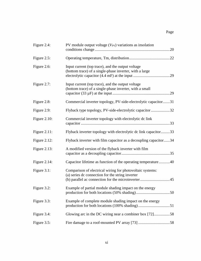
xi
Page
Figure 2.4: PV module output voltage (VPV) variations as insolation
conditions change ............................................................................ 20
Figure 2.5: Operating temperature, Tm, distribution ......................................... 22
Figure 2.6: Input current (top trace), and the output voltage
(bottom trace) of a single-phase inverter, with a large
electrolytic capacitor (4.4 mF) at the input ..................................... 29
Figure 2.7: Input current (top trace), and the output voltage
(bottom trace) of a single-phase inverter, with a small
capacitor (33 µF) at the input .......................................................... 29
Figure 2.8: Commercial inverter topology, PV-side-electrolytic capacitor ....... 31
Figure 2.9: Flyback type topology, PV-side-electrolytic capacitor ................... 32
Figure 2.10: Commercial inverter topology with electrolytic dc link
capacitor .......................................................................................... 33
Figure 2.11: Flyback inverter topology with electrolytic dc link capacitor ......... 33
Figure 2.12: Flyback inverter with film capacitor as a decoupling capacitor ...... 34
Figure 2.13: A modified version of the flyback inverter with film
capacitor as a decoupling capacitor ................................................. 35
Figure 2.14: Capacitor lifetime as function of the operating temperature ........... 40
Figure 3.1: Comparison of electrical wiring for photovoltaic systems:
(a) series dc connection for the string inverter
(b) parallel ac connection for the microinverter .............................. 45
Figure 3.2: Example of partial module shading impact on the energy
production for both locations (50% shading) .................................. 50
Figure 3.3: Example of complete module shading impact on the energy
production for both locations (100% shading) ................................ 51
Figure 3.4: Glowing arc in the DC wiring near a combiner box [72] ................ 58
Figure 3.5: Fire damage to a roof-mounted PV array [73] ................................ 58

xii
Page
Figure 3.6: Possible arc faults locations in string inverter ................................. 59
Figure 4.1: Basic microinverter’s configurations .............................................. 63
Figure 4.2: Single-phase grid-connected PV system ......................................... 64
Figure 4.3: The total power processed by the decoupling capacitor.................. 66
Figure 4.4: I-V and P-V characteristic of a PV module ..................................... 67
Figure 4.5: Single stage inverter ........................................................................ 70
Figure 4.6: Multi-stage inverter ......................................................................... 71
Figure 4.7: Employing power stage to realize power decoupling on
the PV side ...................................................................................... 73
Figure 4.8: Topology proposed by Kyritsis, et al [78] ...................................... 75
Figure 4.9: Power decoupling control strategy .................................................. 75
Figure 4.10: Topology proposed by Shimizu, et al [44] ...................................... 76
Figure 4.11: Magnetizing currents at primary side .............................................. 76
Figure 4.12: Modified topology proposed by Kjaer, et al [39] ............................ 77
Figure 4.13: Key waveforms in one switching cycle ........................................... 78
Figure 4.14: Topology proposed by Hu, et. al [82] ............................................. 79
Figure 4.15: Topology proposed by Harb, et. al [83] .......................................... 79
Figure 4.16: Key waveforms for topologies in Figure 4.14 and 4.15 .................. 80
Figure 4.17: Topology proposed by Shinjo, et. al [84] ........................................ 81
Figure 4.18: The driver signal for the topology in Figure 4.17 ........................... 81
Figure 4.19: Topology proposed by Hirao, et al [85] .......................................... 82
Figure 4.20: Magnetizing current and driver signals for the topology
in Figure 4.19 .................................................................................. 82

xiii
Page
Figure 4.21: Topology proposed by Chen, et. al [86] .......................................... 84
Figure 4.22: Key waveform for topology in Figure 4.21 ..................................... 84
Figure 4.23: Topology proposed by Li, et. al [87] .............................................. 84
Figure 4.24: Operation modes and driving signals for the topology
in Figure 4.23 .................................................................................. 85
Figure 4.25: Topology proposed by Tan, et. al [88] ............................................ 86
Figure 4.26: Key waveforms for the topology in Figure 4.25 ............................. 86
Figure 4.27: DC link voltage and the output AC voltage waveforms [89] .......... 87
Figure 4.28: Allowed maximum DC voltage ripple [90] ..................................... 88
Figure 4.29: Modulation technique proposed by Enjeti, et. al [94] ..................... 89
Figure 4.30: Control scheme proposed by Brekken, et. al [95] ........................... 89
Figure 4.31: Voltage-ripple estimation strategy for large DC ripple
proposed by Ninad, et. al [96] ......................................................... 90
Figure 4.32: Topology proposed by Li, et. al [100] ............................................ 91
Figure 4.33: Topology proposed by Bush, et. al [101] ........................................ 92
Figure 4.34: Topology proposed by Shimizu, et al [102] .................................... 92
Figure 4.35: Topology proposed by Tsuno, et al [103] ....................................... 93
Figure 4.36: The power process in the PV system with power
decoupling circuit ............................................................................ 96
Figure 4.37: An integrated three-port inverter with power decoupling
capability [104] ............................................................................. 100
Figure 4.38: AC link implementation of three-port converter proposed
in [105] .......................................................................................... 100
Figure 5.1: A general system block diagram of the ripple-port ....................... 103

xiv
Page
Figure 5.2: System block diagram of the ripple-port module-integrated
inverter (RP-MII) .......................................................................... 105
Figure 5.3: Ripple-port schematic ................................................................... 106
Figure 5.4: Ripple-port module-integrated inverter, single winding ............... 108
Figure 5.5: Ripple-port module-integrated inverter, multiple windings .......... 109
Figure 5.6: Low pass filter block diagrm ......................................................... 111
Figure 5.7: Theoretical voltage waveform of a single-phase
grid-connected PV System ............................................................ 115
Figure 5.8: Theoretical power waveform of a single-phase
grid-connected PV System ............................................................ 116
Figure 5.9: The relationship between the DoMRP and the operating
power at different decoupling capacitor (CD) design values ......... 118
Figure 5.10: Block diagram of a candidate SPWM control scheme used to
control both the output and the ripple-port inverters.
In practice, a deadtime would need to be added to ensure no
shoot-through condition ................................................................ 120
Figure 5.11: PSIM simulation schematic of the ripple-port
module-integrated inverter, single winding................................... 124
Figure 5.12: DC-Link, output, and decoupling capacitor voltage ..................... 125
Figure 5.13: Simulation shows operation of cancels double-line frequency ..... 125
Figure 5.14: Zoom in of the input power waveform, from Figure 5.13,
showing attenuation of the double-frequency ripple ..................... 126
Figure 5.15: FFT of the input power waveform ................................................ 126
Figure 5.16: Double-line frequency ripple as a function of DoMRP and
phase shift (ϕ) ................................................................................ 128
Figure 5.17: Ripple-port experiment set up ....................................................... 130
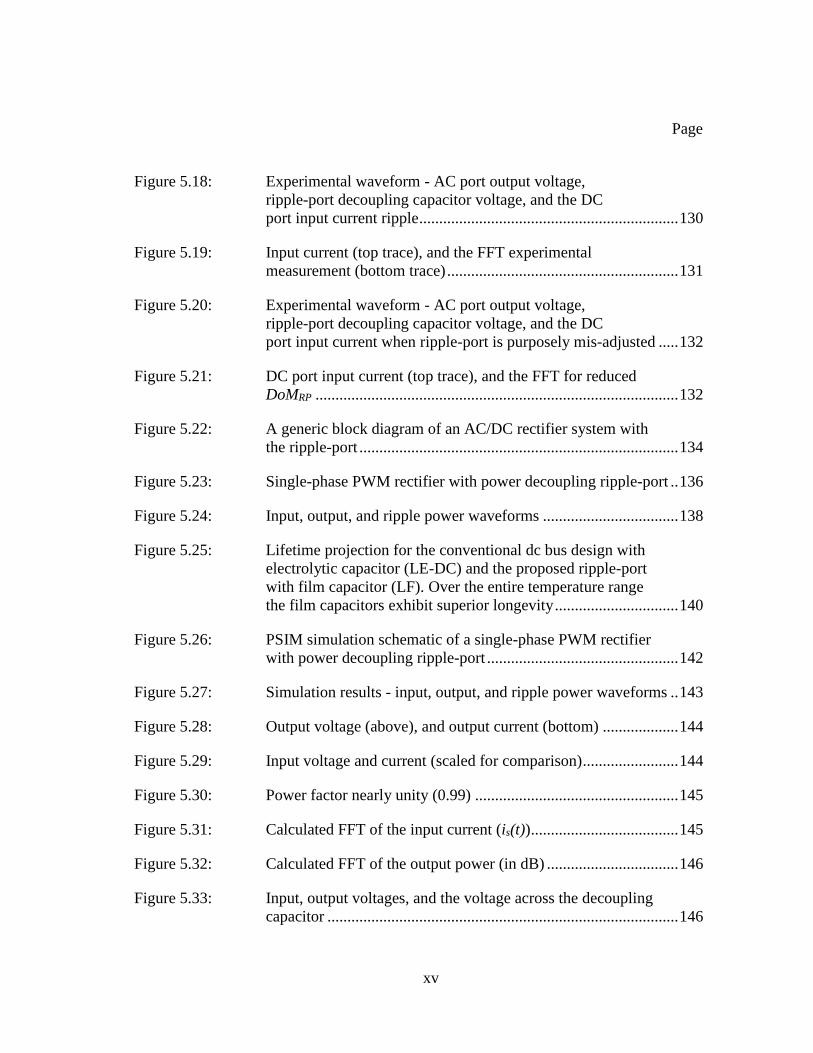
xv
Page
Figure 5.18: Experimental waveform - AC port output voltage,
ripple-port decoupling capacitor voltage, and the DC
port input current ripple ................................................................. 130
Figure 5.19: Input current (top trace), and the FFT experimental
measurement (bottom trace) .......................................................... 131
Figure 5.20: Experimental waveform - AC port output voltage,
ripple-port decoupling capacitor voltage, and the DC
port input current when ripple-port is purposely mis-adjusted ..... 132
Figure 5.21: DC port input current (top trace), and the FFT for reduced
DoMRP ........................................................................................... 132
Figure 5.22: A generic block diagram of an AC/DC rectifier system with
the ripple-port ................................................................................ 134
Figure 5.23: Single-phase PWM rectifier with power decoupling ripple-port .. 136
Figure 5.24: Input, output, and ripple power waveforms .................................. 138
Figure 5.25: Lifetime projection for the conventional dc bus design with
electrolytic capacitor (LE-DC) and the proposed ripple-port
with film capacitor (LF). Over the entire temperature range
the film capacitors exhibit superior longevity ............................... 140
Figure 5.26: PSIM simulation schematic of a single-phase PWM rectifier
with power decoupling ripple-port ................................................ 142
Figure 5.27: Simulation results - input, output, and ripple power waveforms .. 143
Figure 5.28: Output voltage (above), and output current (bottom) ................... 144
Figure 5.29: Input voltage and current (scaled for comparison) ........................ 144
Figure 5.30: Power factor nearly unity (0.99) ................................................... 145
Figure 5.31: Calculated FFT of the input current (is(t)) ..................................... 145
Figure 5.32: Calculated FFT of the output power (in dB) ................................. 146
Figure 5.33: Input, output voltages, and the voltage across the decoupling
capacitor ........................................................................................ 146

xvi
Page
Figure 5.34: Single-phase AC/DC rectifier with ripple-port - experiment
setup .............................................................................................. 148
Figure 5.35: Single-phase AC/DC rectifier with ripple-port – experiment
schematic ....................................................................................... 148
Figure 5.36: Experimental results: DC-link output voltage (ch.3),
decoupling LC filter’s current (ch.2), and input (ch.1) and
decoupling capacitor (ch.4) voltage waveforms
(with ripple-port) ........................................................................... 149
Figure 5.37: The experimentally measured FFT of the DC-link output
voltage (with ripple-port) .............................................................. 150
Figure 5.38: Experimental results: DC-link output voltage (ch.3),
decoupling LC filter’s current (ch.2), and input (ch.1) and
decoupling capacitor (ch.4) voltage waveforms
(without ripple-port) ...................................................................... 151
Figure 5.39: The experimentally measured FFT of the DC-link output
voltage (without ripple-port) ......................................................... 151
Figure 6.1: Ripple-port module-integrated inverter (RP-MII) ......................... 155
Figure 6.2: DC-link module-integrated inverter (DC-MII) ............................. 155
Figure 6.3: Pictorial illustration of the capacitance decrement with time ....... 160
Figure 6.4: Aluminum electrolytic and metalized polypropylene film
capacitors – comparison ................................................................ 163
Figure 6.5: MOSFET's power losses distribution ............................................ 170
Figure 7.1: A general system block diagram of AC-link based ripple-port..... 173
Figure 7.2: AC link ripple-port concept – separate winding configuration ..... 173
Figure 7.3: AC link ripple-port concept – integrated single winding .............. 174
Figure 7.4: Two possible converters for DC/AC stage at the PV-side ............ 174
Figure 7.5: AC-link based inverter with an integrated ripple-port .................. 176

xvii
Page
Figure 7.6: Bidirectional switch configuration: (a) common-source,
(b) common-drain configurations .................................................. 176
Figure 7.7: Control Circuit: high-frequency AC/AC converter driving
signals generation .......................................................................... 177
Figure 7.8: Possible conduction conditions ..................................................... 178
Figure 7.9: The transitions between the conduction states .............................. 179
Figure 7.10: All possible transitions and the commutation process .................. 181
Figure 7.11: Four-step switching technique (Vlink is positive) ........................... 182
Figure 7.12: Four-step switching technique (Vlink is negative) .......................... 184
Figure 7.13: Current commutation when switching from Q1, Q4 to Q2, Q3
(Vlink is positive) ............................................................................ 186
Figure 7.14: Current commutation when switching from Q2, Q3 to Q1, Q4
(Vlink is negative) ............................................................................ 186
Figure 7.15: The output voltage, v0, and the voltage across the decoupling
capacitor, vCD ................................................................................. 187
Figure 7.16: Input, output, and ripple-port power waveforms ........................... 188
Figure 7.17: Input current waveform ................................................................. 189
Figure 7.18: Calculated FFT of the input current .............................................. 189
Figure 7.19: Input power waveform .................................................................. 190
Figure 7.20: Calculated FFT of the input power ............................................... 190
Figure 7.21: Experimental setup of the proposed topology - PV-mode
operation ........................................................................................ 191
Figure 7.22: Measured FFT of the Input current without the ripple-port .......... 192
Figure 7.23: Measured FFT of the Input current with the ripple-port ............... 192
xviii
Page
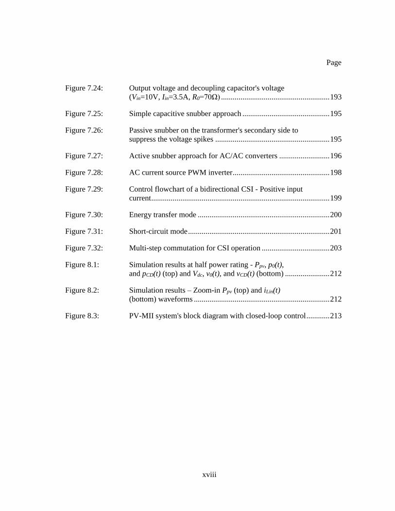
Figure 7.24: Output voltage and decoupling capacitor's voltage
(Vin=10V, Iin=3.5A, R0=70Ω) ........................................................ 193
Figure 7.25: Simple capacitive snubber approach ............................................. 195
Figure 7.26: Passive snubber on the transformer's secondary side to
suppress the voltage spikes ........................................................... 195
Figure 7.27: Active snubber approach for AC/AC converters .......................... 196
Figure 7.28: AC current source PWM inverter .................................................. 198
Figure 7.29: Control flowchart of a bidirectional CSI - Positive input
current ............................................................................................ 199
Figure 7.30: Energy transfer mode .................................................................... 200
Figure 7.31: Short-circuit mode ......................................................................... 201
Figure 7.32: Multi-step commutation for CSI operation ................................... 203
Figure 8.1: Simulation results at half power rating - Ppv, p0(t),
and pCD(t) (top) and Vdc, v0(t), and vCD(t) (bottom) ....................... 212
Figure 8.2: Simulation results – Zoom-in Ppv (top) and iLin(t)
(bottom) waveforms ...................................................................... 212
Figure 8.3: PV-MII system's block diagram with closed-loop control ............ 213
xix
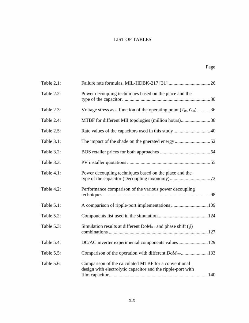
LIST OF TABLES
Page
Table 2.1: Failure rate formulas, MIL-HDBK-217 [31] .................................. 26
Table 2.2: Power decoupling techniques based on the place and the
type of the capacitor ........................................................................ 30
Table 2.3: Voltage stress as a function of the operating point (Tm, Gm) ........... 36
Table 2.4: MTBF for different MII topologies (million hours) ........................ 38
Table 2.5: Rate values of the capacitors used in this study .............................. 40
Table 3.1: The impact of the shade on the gnerated energy ............................. 52
Table 3.2: BOS retailer prices for both approaches ......................................... 54
Table 3.3: PV installer quotations .................................................................... 55
Table 4.1: Power decoupling techniques based on the place and the
type of the capacitor (Decoupling taxonomy) ................................. 72
Table 4.2: Performance comparison of the various power decoupling
techniques ........................................................................................ 98
Table 5.1: A comparison of ripple-port implementations .............................. 109
Table 5.2: Components list used in the simulation ......................................... 124
Table 5.3: Simulation results at different DoMRP and phase shift (ϕ)
combinations ................................................................................. 127
Table 5.4: DC/AC inverter experimental components values ........................ 129
Table 5.5: Comparison of the operation with different DoMRP ...................... 133
Table 5.6: Comparison of the calculated MTBF for a conventional
design with electrolytic capacitor and the ripple-port with
film capacitor ................................................................................. 140

xx
Page
Table 5.7: AC/DC rectifier with ripple-port simulation parameters .............. 141
Table 5.8: AC/DC rectifier experimental components values ........................ 147
Table 5.9: Comparison of operating the AC/DC system with and
without the ripple-port ................................................................... 152
Table 6.1: Two electrolytic capacitor options ................................................ 159
Table 6.2: Parallel capacitors option .............................................................. 163
Table 6.3: Switching power loss calculations ................................................ 168
Table 6.4: Paralleled capacitors implementation comparison ........................ 169
Table 6.5: MOSFET power loss ..................................................................... 170
Table 7.1: All possible static switch states ..................................................... 177
Table 7.2: Simulation parameters ................................................................... 185

1
1 INTRODUCTION
1.1 National energy and technical challenges
The Department of Energy (DOE) has identified a number of energy challenges that are
necessary to upgrade into the future smart grid [1]. Figure 1.1 summarizes these challenges
and illustrates how the field of Power Electronics has a very important role in bridging the
gap between the national energy and the technology challenges that will eventually
facilitate the transition into the future smart grid.
Figure 1.1: National energy and technology challenges
Energy
Independence
And
Affordability
Energy
reliability,
security and
efficiency
Economic
development
and job
security
Environmental
concerns and
impact of
climate
change
National Energy Challenges
Renewable
resources
technologies
Energy
efficiency
Electric
transportation
Energy
storage
Technology Challenges
Power ElectronicsFuture Grid that
evolves to enable
new solutions

2
With the depletion of fossil fuels, renewable sources, generated from natural resources,
have caught the eye in recent years from both the industries and governments worldwide
due to their environmental friendliness, sustainability nature, economic benefits, and
energy security. Figure 1.2 shows the investment growth in the Renewable Energy field
during the last decade, which shows an exponential growth [2].
Figure 1.2: Global new investment in Renewable Energy by asset class, 2004-2012, [2]
In the United States, Renewable Energy counts for 11.2% of the total Energy production
for 2012, as shown in Figure 1.3 [3]. Although Wind Energy and Solar Energy only count
for 2% of the Renewable energy production, they are the two Renewable energy sources
with the highest growing rate in the last decade, as show in Figure 1.4. Wind and

3
Photovoltaic (PV) Energy resources were the fastest growing technologies, as shown in
Figure 1.4. In 2012, wind and PV energy have experienced 28% and 83% increment in
cumulative installed capacity, respectively, in the US [3]. To meet the 2020 renewable
energy targets of the European Union, the European Photovoltaic Industry Association
(EPIA) recently estimated that the possible contribution of photovoltaic is up to 12% of
the electricity supply by 2020.
Figure 1.3: Energy production in US for the year of 2012, source: DOE [3]
Figure 1.4: Renewable energy growth in US, source: DOE [3]

4
In 2012, more than 100 GW of PV are installed globally—an amount capable of
producing at least 110 TWh of electricity every year [3]. Moreover, in Figure 1.5, new
players have entered into the PV field. Figure 1.5 shows that United States and China have
doubled and tripled, respectively, their PV installed capacity during the last three years
[4].
Figure 1.5: Evolution of global PV cumulative installed capacity, source: EPIA [4]
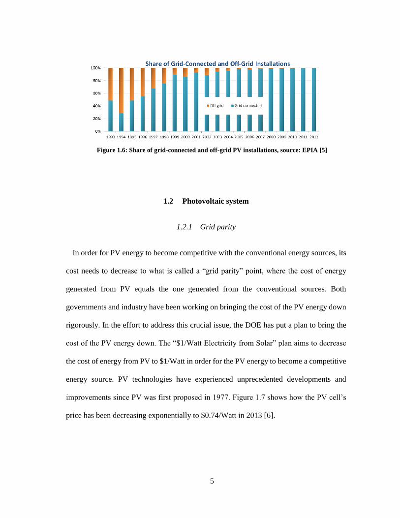
Figure 1.6 shows that grid-connected (AKA “grid-tie”) PV systems represent the largest
share of the market [5]. The Grid-connected PV system has become the trend in the past
decade because no energy storage devices are needed. Energy storage devices have
relatively low lifetime, and high cost.
5
Figure 1.6: Share of grid-connected and off-grid PV installations, source: EPIA [5]
1.2 Photovoltaic system
1.2.1 Grid parity
In order for PV energy to become competitive with the conventional energy sources, its
cost needs to decrease to what is called a “grid parity” point, where the cost of energy
generated from PV equals the one generated from the conventional sources. Both
governments and industry have been working on bringing the cost of the PV energy down
rigorously. In the effort to address this crucial issue, the DOE has put a plan to bring the
cost of the PV energy down. The “$1/Watt Electricity from Solar” plan aims to decrease
the cost of energy from PV to $1/Watt in order for the PV energy to become a competitive
energy source. PV technologies have experienced unprecedented developments and
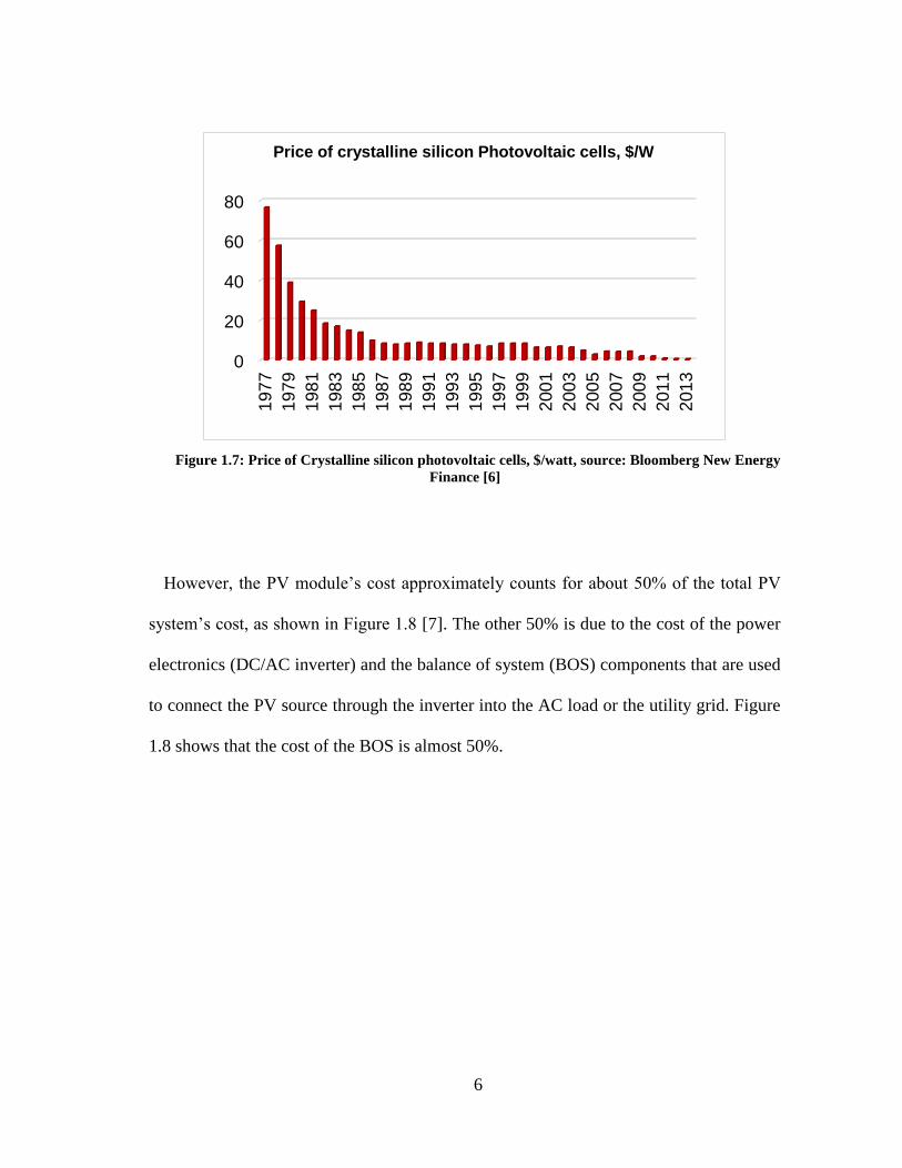
improvements since PV was first proposed in 1977. Figure 1.7 shows how the PV cell’s
price has been decreasing exponentially to $0.74/Watt in 2013 [6].
6
Figure 1.7: Price of Crystalline silicon photovoltaic cells, $/watt, source: Bloomberg New Energy
Finance [6]
However, the PV module’s cost approximately counts for about 50% of the total PV
system’s cost, as shown in Figure 1.8 [7]. The other 50% is due to the cost of the power
electronics (DC/AC inverter) and the balance of system (BOS) components that are used
to connect the PV source through the inverter into the AC load or the utility grid. Figure
1.8 shows that the cost of the BOS is almost 50%.
0
20
40
60
80
197
7
197
9
198
1
198
3
198
5
198
7
198
9
199
1
199
3
199
5
199
7
199
9
200
1
200
3
200
5
200
7
200
9
201
1
201
3
Price of crystalline silicon Photovoltaic cells, $/W

7
Figure 1.8: The Prospect for $1/Watt Electricity from Solar, source: DOE [7]
1.2.2 Photovoltaic system configurations
Grid-connected PV systems are categorized into three categories: centralized inverter,
string inverter, and AC-Module “microinverter” [8-10]. Microinverter or Module-
Integrated-Inverter (MII), with power levels ranging from 150W to 300W, has become the
trend for grid-connected PV systems due to its numerous advantages including: improved
energy harvest, improved system efficiency, lower installation costs, “Plug-N-Play”
operation, and enhanced modularity and flexibility. However many challenges remain in
the way of achieving low manufacturing costs, high conversion efficiencies, and long life
span. Since MII is typically attached to the back of the PV module, and may be well
integrated to the PV module back skin, it is desirable that the inverter has a lifetime that

8
matches the PV module one. It is well known that electrolytic capacitors are the limiting
components that determine the lifetime of the microinverter [11]. The aforementioned
advantages of the integration of the power electronics into the PV Module does not come
for free, the reliability of the power electronics should match the PV module’s one, namely
25 years [8, 9, 12].
Figure 1.9: Photovoltaic (PV) system configurations
1.3 LED lighting – Energy efficiency
According to [13] it was found that one-fifth of the world-wide electricity is consumed
in lighting applications. In the US, 17% of the total electricity is used for lighting [14].
DC
AC
PV
-Modu
le
Grid
PV
-Modu
le
Grid
DC
AC
PV
-Modu
le
Grid
DC
AC
Strin
gs P
V S
yste
m
PV
-Modu
le
PV
-Modu
le
DC
AC
Grid
DC
DC
DC
DC
Mu
lti-Strin
g P
V S
ystem
Grid
DC
AC
PV
-Modu
le
1980’s
Bulky, heavy, unreliable,
and difficult to install
85 – 90% efficiency
1995
Higher system efficiency
and reliability
efficiencies above 95%
2000’s
MPPT at the module
level higher efficiency
and reliability

9
The most commonly used lighting sources include incandescent bulbs and fluorescent
lamps. However, these lighting sources have reported a relatively low efficiency.
Recently, a new form of fluorescent lights, the compact fluorescent lamp (CFL), has
becoming more popular in the lighting industry, which is known as “energy-saving light”
because of its higher efficiency compared to the old technologies. However, CFL lights
still suffer from a low lifetime. Thus, a new more efficient, high-reliable, and cost effective
lighting source has been proposed using LED semiconductors. Figure 1.10 shows the three
different lighting technologies and their advantages. LEDs have attracted the attention in
last few years due its many advantages: high efficiency, small size (compactness), light
weight, robustness, long lifetime (high reliability), and environmental friendliness [13,
15].
Figure 1.10: The evolution of the lighting technology
No Power Electronics
Integrated
Power ElectronicsIntegrated
Power Electronics
Higher Efficiency
Higher Lifetime
Relatively Higher
Efficiency
Incandescent Light
Compact Fluorescent
Light (CFL)LED Light
Low Efficiency
10
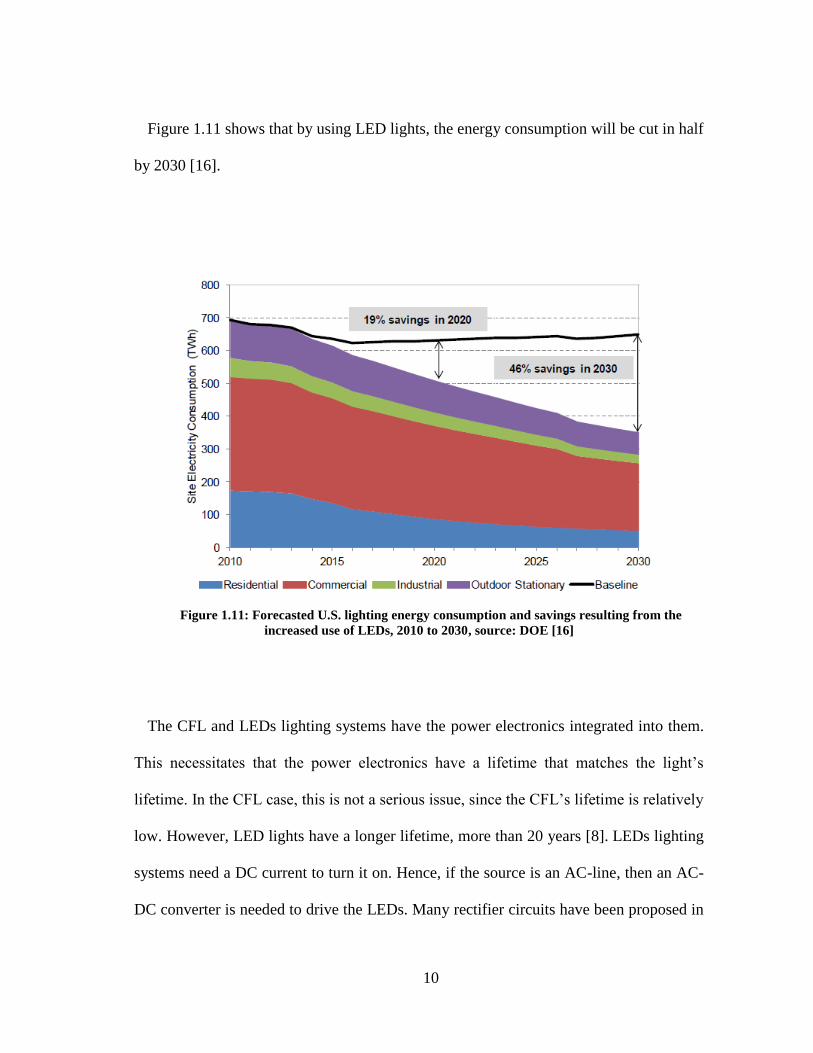
Figure 1.11 shows that by using LED lights, the energy consumption will be cut in half
by 2030 [16].
Figure 1.11: Forecasted U.S. lighting energy consumption and savings resulting from the
increased use of LEDs, 2010 to 2030, source: DOE [16]
The CFL and LEDs lighting systems have the power electronics integrated into them.
This necessitates that the power electronics have a lifetime that matches the light’s
lifetime. In the CFL case, this is not a serious issue, since the CFL’s lifetime is relatively
low. However, LED lights have a longer lifetime, more than 20 years [8]. LEDs lighting
systems need a DC current to turn it on. Hence, if the source is an AC-line, then an AC-
DC converter is needed to drive the LEDs. Many rectifier circuits have been proposed in

11
the literature [15, 17]. Based on the number of conversion stages and the number of phases,
theses rectifier topologies can be categorized into four types: single-phase single-stage,
single-phase multi-stage, three-phase single stage, and three-phase multi-stage [17]. The
single-phase PWM rectifier has numerous advantages over classical passive rectifier
topologies including: unity power factor, low THD, bidirectional power flow, and low
components count [18, 19], and is well suited for applications with power ranging from
data center servers to LED lighting.
1.4 Dissertation outline
This thesis deals with the reliability of the integrated power electronics that are used in
uncontrolled operating environments, such as: renewable energy applications, LED
lighting systems, etc. Operating in such an environment imposes very harsh, volatile, and
wide-range conditions on the power electronic converters. And thus, evaluating the
reliability of these converters becomes more involved task. The study is divided into two
main aspects: (1) a new methodology for evaluating the integrated power electronics; and
(2) a new power decoupling technique for the single-phase DC/AC and AC/DC
converters, which will improve the reliability. The remainder of this dissertation is
organized as follows.
In section 2, the reliability of integrated power electronics is thoroughly investigated
taking into account the usage model. PV module-integrated-inverter (MII) is considered
as a case study, and a comparative study of the reliability for different PV-MII topologies
is performed.

12
In section 3, the PV-MII configuration is compared against the string PV system
configuration. A typical 6 kW residential PV system is designed considering both PV
configurations. Reliability, environmental factors, inverter failure, and electrical safety
are the main factors that are investigated and evaluated.
In section 4, the double-line frequency ripple problem is presented alongside its negative
effects. Different decoupling techniques are presented and categorized based on the
decoupling capacitor place.
In section 5, the DC-link based ripple-port technique for double-line-frequency ripple
cancellation is presented. The ripple-port concept is implemented and tested in DC/AC
inverting mode and AC/DC rectifying mode. Analysis, simulation, and experimental
results are presented.
In section 6, the AC-link ripple-port topology is presented. Similarly, analysis
simulation results are presented. Practical experimental limitations for the proposed
topology implementation and possible solutions are presented.
In Section 7, the DC-link ripple-port MII is compared to the conventional DC-link MII.
Based on the assumption that both configuration offer the same lifetime, efficiency, power
density, and cost of each configuration are studied and presented.
Finally, Section 8 is a summary and conclusion of the work presented in this dissertation.
Also, possible future work on this subject is presented.

13
2 TAXONOMY, USAGE MODEL, AND RELIABILITY *
The trend in power electronics is to integrate the electronics into the source (PV) or the
load (light). For PV and outdoor lighting applications, this imposes a harsh, wide-range
operating environment on the power electronics. Thus, the reliability of power electronics
converters becomes a very crucial issue. It is required that the power electronics, used in
such harsh and uncontrolled environments, have reliability indices, namely: lifetime that
matches the lifetime of the source or the load. For example, integrating the inverter with
the PV module necessitates that the integrated-inverter has a lifetime that matches the PV
module, 25 years or more [8, 20, 21]. This eliminates the reoccurring cost of inverter
replacement that haunts current PV system return on investment (ROI). The reoccurring
cost is further extended in a PV- Module-Integrated-Inverter (MII) since the electronics
are exposed to a harsher environment than in the past when the inverter was mounted
indoors [22, 23]. Similarly in LED applications, the power electronic circuit is integrated
into the LED lighting; since the LED has a high lifetime—more than 20 years—the power
electronics are desired to have a lifetime that matches that of the LED.
Relatively high-efficiency topologies have been reported in the literature [9], and
* © 2012 IEEE. Reprinted, with permission, from S. Harb and R.S. Balog, “Reliability of Candidate
Photovoltaic Module-Integrated-Inverter Topologies,” 27th Annual IEEE Applied Power Electronics
Conference and Exposition (APEC), February, 2012. © 2012 IEEE. Reprinted, with permission, from S.
Harb and R.S. Balog, “Reliability of a PV-Module Integrated Inverter (PV-MII): A Usage Model
Approach,” 38th IEEE Photovoltaic Specialists Conference (PVSC), June, 2012. © 2013 IEEE. Reprinted,
with permission, from S. Harb and R.S. Balog, “Reliability of Candidate Photovoltaic Module-Integrated-
Inverter (PV-MII) Topologies—A Usage Model Approach,” IEEE Transactions on Power Electronics, June,
2013.

14
standards have been developed to measure the efficiency [24]. However, the reliability
aspect has not received the same level of scrutiny. The emergence of the ACPV module
in which the power electronics are directly mounted to the PV module has led to the start
of a rigorous study of the reliability of the PV inverter [25-29]. The recent surge of interest
in cost-effective renewable energy has accordingly focused attention on the balance of
system (BOS), including the power electronics needed to convert generated power into a
useful form and facilitate the penetration of these resources to the utility grid [30].
Although not everyone agrees with the methodology or underlying data, MIL-HDBK-217
[31] has long been considered a standard for computing Mean Time Between Failure
(MTBF) as an assessment of reliability, and thus serves as an excellent relative yardstick
for comparison. MIL-HDBK-217 is based on probability distribution and it is not a
demonstration of actual life of the specific device nor does it seek to identify failure
modes. As such, testing a small sample of units to failure may not result in exactly identical
results to the MTBF prediction. However, the MIL-HDBK-217 approach instead takes
into account statistically large samples sizes of individual components and applies an
acceleration factor based on the various component stresses—in the case in this study, for
example, power dissipation and ambient temperature. Operation time and operating
environment are important conditions that strongly affect the reliability of power
electronics. Evaluating inverter’s reliability at just one single operating condition, for
example, the worst operating condition, leads in most cases to unrealistically low and
pessimistic results, which require more expensive components to mitigate.
In this section, a new methodology to calculate the MTBF of a PV-MII is presented,

15
which takes into consideration the usage model of the inverter—the statistical distribution
of expected operating temperature and power processed rather than a single (worst-case)
operating point. Then, six different inverter topologies, suitable for a MII, will be studied
in the scope of reliability [8, 9]. This section is organized as follows: the usage model for
PV-MII is developed in the next section, and then different ways for calculating the MTBF
is presented in 2.2. The proposed methodology is applied on different MII topologies in
2.3 followed by the reliability and lifetime results in 2.4 and 2.5, respectively.
2.1 Usage model for reliability evaluation
Operating conditions can be either experimentally measured data or predicted by a
thermal model [22]. Although the actual measurements result in accurate reliability
predictions, it is more complex because of the need for an experimental setup and long
time to collect a meaningful set of data. On the other hand, using thermal analytical models
eliminates the aforementioned disadvantages, but on the expense of the accuracy. A
combination of both experimental measurement and thermal model prediction could
potentially give accurate, fast, and less expensive measurements.
2.1.1 Developing a usage model
In this section, an electrical model is developed using expected operating points. Either
from a thermal model [22] or experimentally measured data, it is possible to obtain the
range of operating points for temperature and insolation level (Tm, Gm) in pairs as follows:
(Operating temperature (Tm), Insolation Level (W/m2), Gm).
16
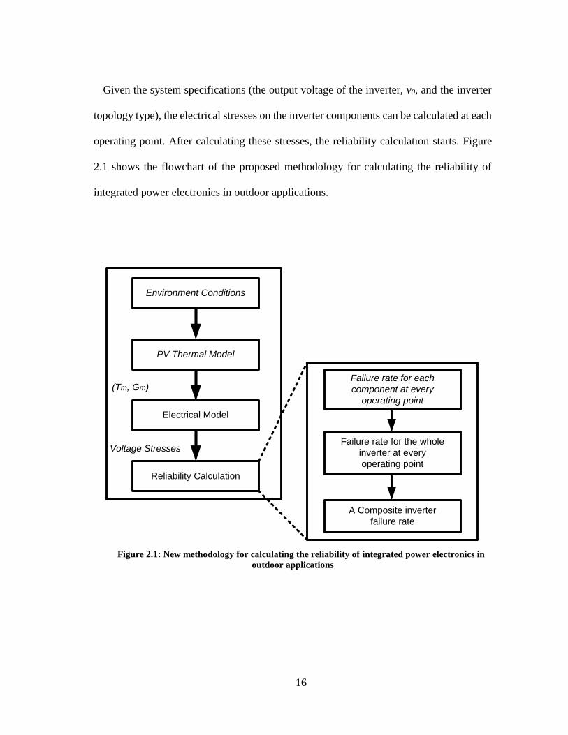
Given the system specifications (the output voltage of the inverter, v0, and the inverter
topology type), the electrical stresses on the inverter components can be calculated at each
operating point. After calculating these stresses, the reliability calculation starts. Figure
2.1 shows the flowchart of the proposed methodology for calculating the reliability of
integrated power electronics in outdoor applications.
Figure 2.1: New methodology for calculating the reliability of integrated power electronics in
outdoor applications
Environment Conditions
PV Thermal Model
Electrical Model
Reliability Calculation
Failure rate for each
component at every
operating point
Failure rate for the whole
inverter at every
operating point
A Composite inverter
failure rate
Voltage Stresses
(Tm, Gm)
17
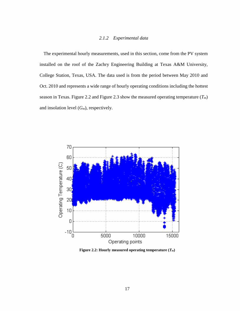
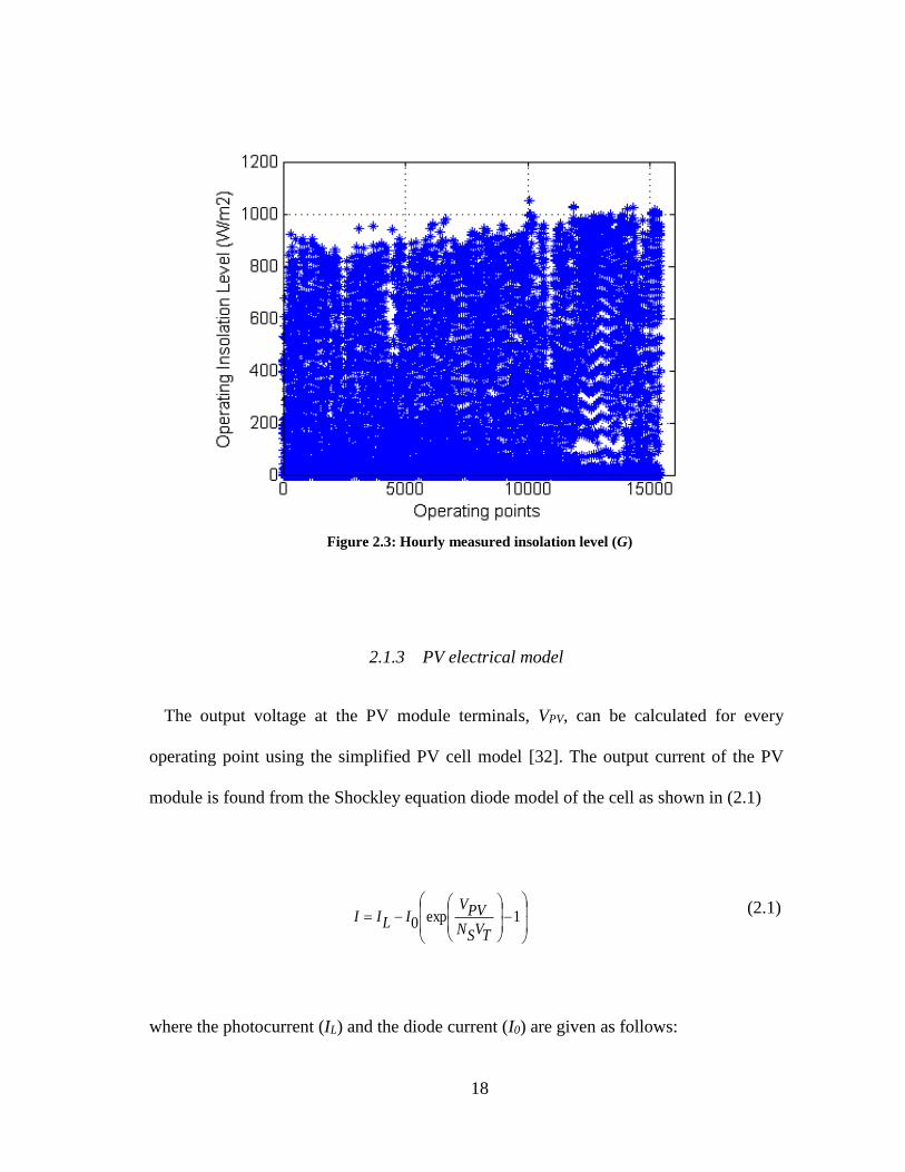
2.1.2 Experimental data
The experimental hourly measurements, used in this section, come from the PV system
installed on the roof of the Zachry Engineering Building at Texas A&M University,
College Station, Texas, USA. The data used is from the period between May 2010 and
Oct. 2010 and represents a wide range of hourly operating conditions including the hottest
season in Texas. Figure 2.2 and Figure 2.3 show the measured operating temperature (Tm)
and insolation level (Gm), respectively.
Figure 2.2: Hourly measured operating temperature (Tm)
18
Figure 2.3: Hourly measured insolation level (G)
2.1.3 PV electrical model
The output voltage at the PV module terminals, VPV, can be calculated for every
operating point using the simplified PV cell model [32]. The output current of the PV
module is found from the Shockley equation diode model of the cell as shown in (2.1)
1exp0
TVSN
PVVILII
(2.1)
where the photocurrent (IL) and the diode current (I0) are given as follows:
19
rTmTKrTLILI 01
(2.2)
rTmTnk
gqVn
rT
mTrTII
11exp
3
00
(2.3)
All parameters in (2.1) – (2.3) can be found in [32].
Since both the voltage and the current of the PV module are unknown, a third equation
is needed. The output power provides this extra equation:
IPVVPVP
1exp0
TVSN
PVVILIPVVPVP
(2.4)
The PV-MII system is assumed to operate at the maximum power point (MPP), a
realistic assumption given the desire to extract maximum energy from the PV system and
the prevalent use of maximum power point tracking controls. Hence, the derivative of the
power in (2.4) with respect to the PV module output voltage is zero, as shown in (2.5)

20
01exp10
kTSN
PVqV
kTSN
PVqVILI
PVdV
PVdP (2.5)
Solving (2.5), for VPV, results in the voltage across the PV module terminals for each
operating point. Figure 2.4 shows VPV as the operating conditions change. From the PV
module voltage, the voltage stresses of components within the inverter can be calculated.
Figure 2.4: PV module output voltage (VPV) variations as insolation conditions change

21
2.2 Reliability prediction calculation
Any reliability calculation standard can be used to calculate the failure rate. In this
section, MIL-HDBK-217 [31] is used because it is freely available unlike other reliability
tools—Telcordia. The failure rate for each component is calculated at every operating
point (Tm, Gm) using MIL-HDBK-217. The failure rate formulas, shown in Table 2.1,
clearly show that operating temperature affects all considered components. The Module
Integrated Inverters are assumed to operate in a benign environment, and according to
MIL-HDBK-217 the environment factor in this case is one (πE=1).
It is worth mentioning that reliability is usually represented by the reciprocal of the
failure rate. The term Mean Time Between Failure (MTBF) is often used interchangeably
with MTTF, which is valid when a failure is not repairable. In most electronic devices,
these values are similar if not identical because of the limited or total lack of reparability
of a failure [33]. Hence, the more common expression MTBF is used in this section with
the understanding that what is meant is really MTTF.
2.2.1 Different methods for calculating the MTBF
The failure rate for the PV-MII is calculated in five different ways:
I. At each operating point (Tm, Gm)
II. The worst case or the minimum MTBF
III. The corner MTBF, which occurs at the maximum temperature and maximum
power (or insolation level)

22
IV. The composite (averaged) MTBF, found from the arithmetic mean as follows:
L
iiMTBF
LavMTBF
1
1 (2.6)
a) MTBFav is the averaged inverter MTBF
b) MTBFi is the inverter MTBF at the ith operating point
c) L is the total number of operating points
V. Finally, since the operating temperature (Tm) affects the failure rate of all
components, its distribution, shown in Figure 2.5, will be used to calculate a
weighted MTBF.
Figure 2.5: Operating temperature, Tm, distribution

23
The results in [22] strongly support the idea of considering all operating temperatures
in calculating the MTBF. Also, the results in [22] show that the PV module temperature
exceeded 80°C for only 2 hours out of the 59,740 total operating hours in the 15 year data
set. Moreover, it shows that the PV module was operating at temperatures less than 60°C
for 95% of the time.
2.2.2 Weighted MTBF
Analysis of the operational data reveals that some operating points occur more
frequently than others, which means that the inverter will be operating at these conditions
more frequently than at others. This can be taken into consideration by calculating a
weighted MTBF. This section does not endorse the merits or suggest improvements to
deficiencies of MIL-HDBK-217, but rather presents a way to use the tool to analyze the
relative differences in reliability of candidate converter topologies. MIL-HDBK-217 does
not include stress factors for every physical failure mode that we as designers must
consider. Indeed there are other analysis tools, such as the Telcordia method that improves
upon MIL-HDBK-217. That said, we feel that the concept of using a reliability index, in
this case MIL-HDBK-217, has merit and deserves to be understood as another way in
which candidate topologies can be compared analytically before committing to a design
and investing time and money into building and testing a prototype. In the formulas shown
in Table 2.1, the temperature is used as an input to the calculation for the failure rate of
each component. Solar insolation also affects the failure rate by varying the input voltage
at the PV module terminals, VPV. According to MIL-HDBK-217 [31], the failure rate
24
formula for the MOSFET, shown in Table 2.1, does not have a voltage stress factor, and
it depends on the following factors: base failure rate (λb_S), which is given in MIL-HDBK-
217, the temperature factor (λT) that depends on the operating temperature as shown in
Table 2.1, the power factor (λA), which is given in MIL-HDBK-217 for different power
ratings, and finally the quality (λQ) and environment (λE) factors, which also are given in
MIL-HDBK-217 and selected for a specific application. Hence, the failure rate of the
MOSFET, according to MIL-HDBK-217, will not be directly affected by the changes in
the applied voltage, since the power rating categories, given in MIL-HDBK-217, are
relatively wide. Hence the input voltage affects just the diode failure rate. As a result, the
temperature has a stronger impact on the MTBF values than the insolation. Therefore,
weight factors based on the operating temperature will be used and a composite MTBF
will be formed from the weighted average failure rates of the operating points.
First, the weight factors are given as follows:
TN
iNiC (2.7)
where:
Ni is number of operating temperature points in the ith temperature range,
NT is the total number of operating temperature points,

25
i= 1, 2, ………Nn, and
Nn is number of intervals, given as:
,minmax
S
TTCeilnN
Ceil is the rounds the number of temperature intervals into the nearest higher integer
S is step in temperature.
Then, the weighted MTBF is calculated as follows:
Nn
kkCkTMTBFMTBFWg
1*)( (2.8)
where:
MTBFWg is the weighted inverter MTBF,
MTBF (Tk) is the MTBF at kT , and
2
1 iTiT
kT , k=1,2,….Nn
Following this procedure leads to a large reduction in the number of total computational
operations required to calculate the average inverter MTBF. Next, the proposed
methodology is applied to evaluate the reliability of potential MII candidates.

26
Table 2.1: Failure rate formulas, MIL-HDBK-217 [31]
Failure Rate (λp)
MOSFET EQATSbnSP _*_
012.0_
Sb
298
1
273
11925exp
mTT
WrPA 250508
5.5Q (Lower)
Diode EQCSTDb
nDP
_
*_
025.0_ Db
298
1
273
13091exp
mTT
13.043.2
3.0054.0
SVSV
SV
S
5.5Q (Lower)
Capacitor EQCVCbn
CP
_*
_
5
378
27309.5exp1
3
5.0
00254.0_mTS
Cb
18.034.0 CCV
10Q (Lower)
Inductor &
Transformer EQTIbn
IP
_*
_
00003.0_ Ib,
019.0_ Trb
298
1
273
1
510*617.8
11.0exp
mTT
3Q (Lower)

27
2.3 Candidate inverter topologies for photovoltaic applications
There are many inverter topologies in the literature that have been proposed in the last
decade for PV applications. Aside from the obvious differences in voltage, power, and
number of phase, these topologies can further be classified according to the number of the
power conversion stages, the power decoupling technique employed, and the presence of
galvanic isolation. For single-phase grid-connected MII, the latter is desirable for safety
purposes. Within a given topology, the capacitor technology used for power decoupling is
a crucial issue [34] as it is widely known to have a significant impact on the reliability of
the inverter, as will be demonstrated in this section.
In a single-phase inverter, a double-line frequency ripple is reflected at the input (DC)
side. In a PV system, this ripple will deteriorate the MPPT performance and consequently
reduce the system total energy harvest. Hence, a storage device is needed to filter out the
double-line frequency ripple. Usually, a capacitor is used to accomplish this task [8, 9, 35-
37]. The double-line-frequency ripple problem is presented in Section 4 in detail. Figure
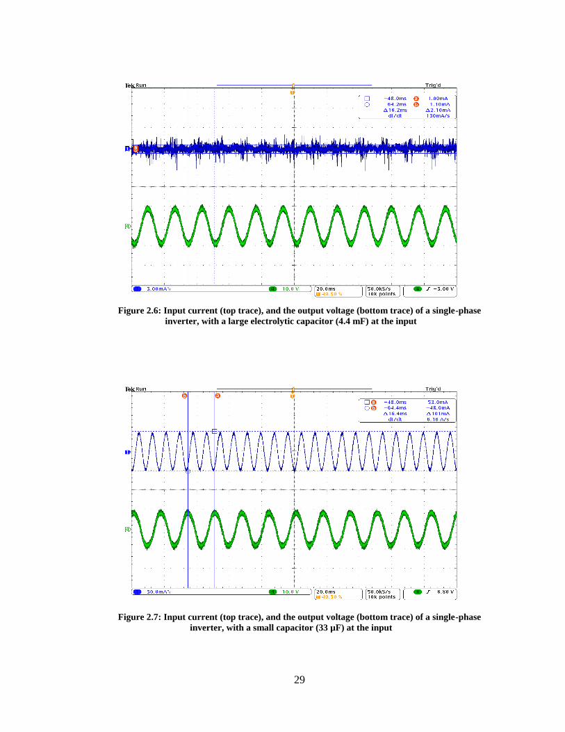
2.6 shows the input current (blue) and the output voltage (green) of a single-phase inverter
that uses an electrolytic capacitor on the input side (4400µF). The results in Figure 2.6
show an almost ripple-free input current. However, when the large, electrolytic capacitor,
used in the previous test, is replace by a another smaller capacitor (33µF) the input current
has a much higher double-line frequency ripple, as shown in Figure 2.7. Figure 2.6 and
Figure 2.7 experimentally justify the necessity of using the capacitor in order to have a
ripple-free input power. Having the double-line frequency ripple on the input side of the
MII results in shifting the MPP operating point away from the optimum operation [8]. The
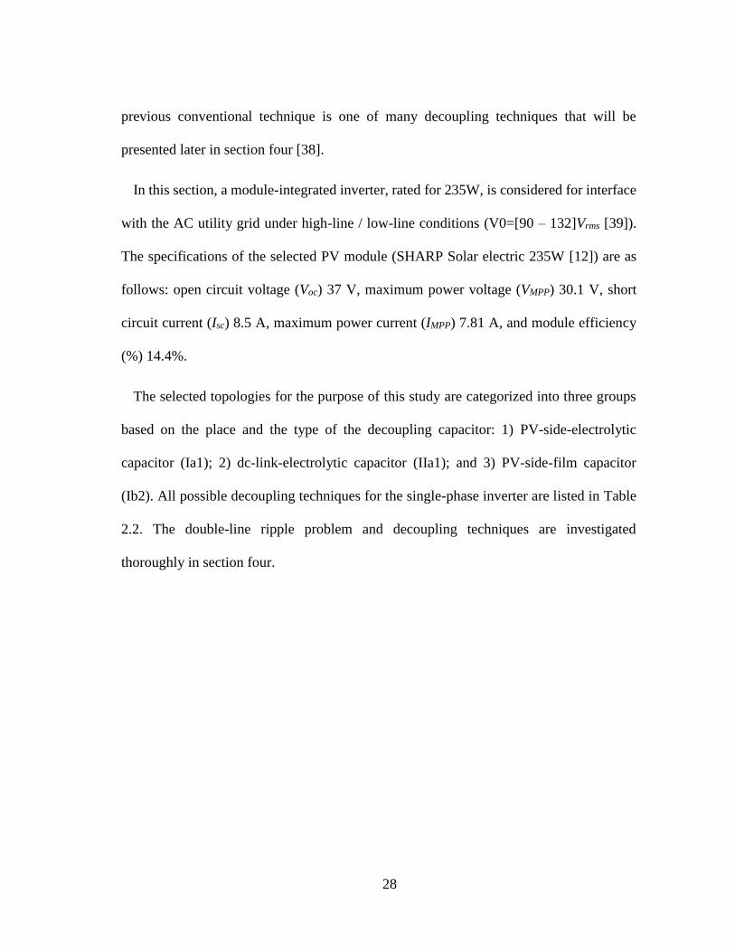
28
previous conventional technique is one of many decoupling techniques that will be
presented later in section four [38].
In this section, a module-integrated inverter, rated for 235W, is considered for interface
with the AC utility grid under high-line / low-line conditions (V0=[90 – 132]Vrms [39]).
The specifications of the selected PV module (SHARP Solar electric 235W [12]) are as
follows: open circuit voltage (Voc) 37 V, maximum power voltage (VMPP) 30.1 V, short
circuit current (Isc) 8.5 A, maximum power current (IMPP) 7.81 A, and module efficiency
(%) 14.4%.
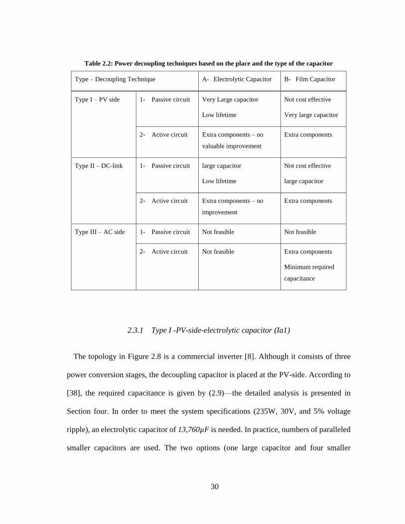
The selected topologies for the purpose of this study are categorized into three groups
based on the place and the type of the decoupling capacitor: 1) PV-side-electrolytic
capacitor (Ia1); 2) dc-link-electrolytic capacitor (IIa1); and 3) PV-side-film capacitor
(Ib2). All possible decoupling techniques for the single-phase inverter are listed in Table
2.2. The double-line ripple problem and decoupling techniques are investigated
thoroughly in section four.
29
Figure 2.6: Input current (top trace), and the output voltage (bottom trace) of a single-phase
inverter, with a large electrolytic capacitor (4.4 mF) at the input
Figure 2.7: Input current (top trace), and the output voltage (bottom trace) of a single-phase
inverter, with a small capacitor (33 µF) at the input
30
Table 2.2: Power decoupling techniques based on the place and the type of the capacitor
Type – Decoupling Technique A- Electrolytic Capacitor B- Film Capacitor
Type I – PV side 1- Passive circuit Very Large capacitor
Low lifetime
Not cost effective
Very large capacitor
2- Active circuit Extra components – no
valuable improvement
Extra components
Type II – DC-link 1- Passive circuit large capacitor
Low lifetime
Not cost effective
large capacitor
2- Active circuit Extra components – no
improvement
Extra components
Type III – AC side 1- Passive circuit Not feasible Not feasible
2- Active circuit Not feasible Extra components
Minimum required
capacitance
2.3.1 Type I -PV-side-electrolytic capacitor (Ia1)
The topology in Figure 2.8 is a commercial inverter [8]. Although it consists of three
power conversion stages, the decoupling capacitor is placed at the PV-side. According to
[38], the required capacitance is given by (2.9)—the detailed analysis is presented in
Section four. In order to meet the system specifications (235W, 30V, and 5% voltage
ripple), an electrolytic capacitor of 13,760µF is needed. In practice, numbers of paralleled
smaller capacitors are used. The two options (one large capacitor and four smaller

31
capacitors) are explored to quantify the effect of number of components.
VDC
Vo
PVP
DC
(2.9)
Figure 2.8: Commercial inverter topology, PV-side-electrolytic capacitor
The same power decoupling technique is employed by the topology in Figure 2.9 [40].
However, this inverter topology consists of single power conversion stage, hence, fewer
components are used. The purpose is to explore the impact of the number of power
components on inverter reliability. Only two diodes and three MOSFETs are needed
compared to four diodes and six MOSFETs needed by the previous topology in Figure
2.8.
S1S2
PV
D1
D2
D3
D4
LDC
Sac1
Sac2
Sac3
Sac4
CPV
Grid
Cf
Lf
1:N

32
Figure 2.9: Flyback type topology, PV-side-electrolytic capacitor
2.3.2 Type II - DC-Link-electrolytic capacitor (IIa1)
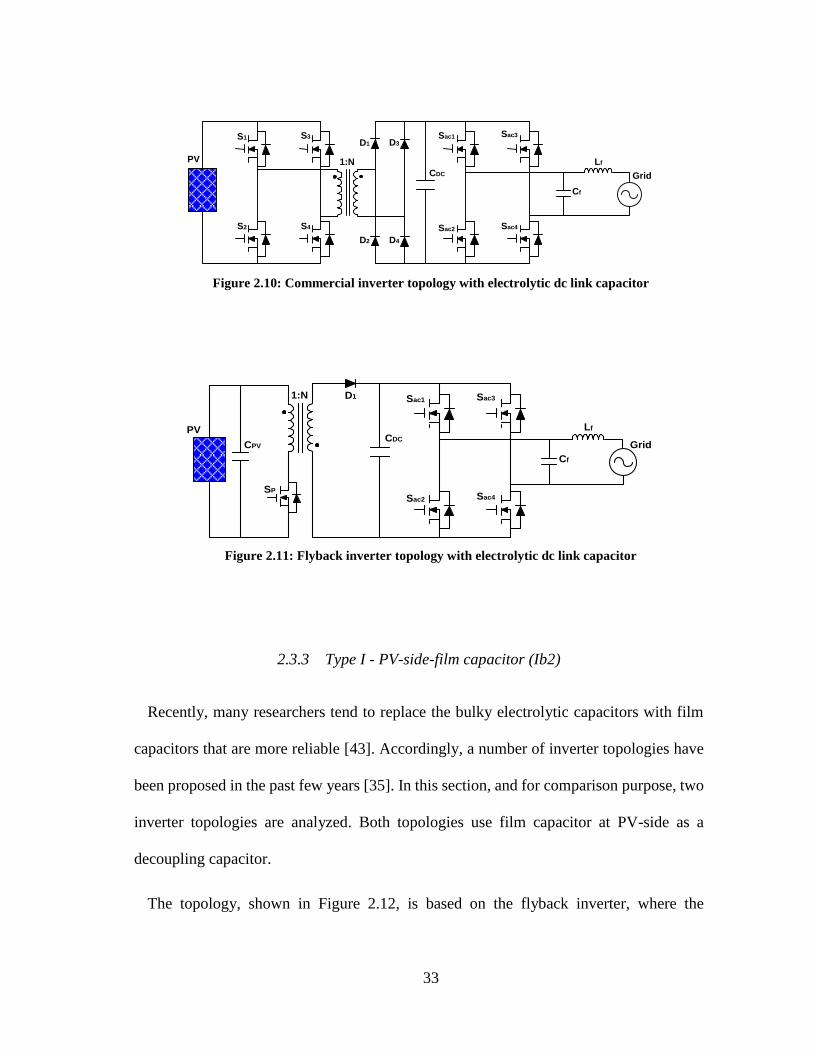
The topology shown in Figure 2.10 is also a commercial inverter [9]. It consists of three
power conversion stages; an inverter and a rectifier, at the front end, are used to provide a
galvanic isolation using high-frequency transformer. The decoupling capacitor is placed
at the DC-link with a relatively higher voltage level. This, in turn, allows for a smaller
capacitance to be used for the same power rating. According to (2.9), a 330µF electrolytic
capacitor is needed to meet the aforementioned specifications. Another topology, shown
in Figure 2.11 [41, 42], also employs the DC-link power decoupling; however, it consists
of two power conversion stages. As a result, fewer components are used. Similarly, this is
meant to study the effect of components other than the decoupling capacitor on the
reliability of the inverter.
CPV Cf
Lf
Grid
SP
Sac1
Sac2
D1
D2
PV
1:N
33
Figure 2.10: Commercial inverter topology with electrolytic dc link capacitor
Figure 2.11: Flyback inverter topology with electrolytic dc link capacitor
2.3.3 Type I - PV-side-film capacitor (Ib2)
Recently, many researchers tend to replace the bulky electrolytic capacitors with film
capacitors that are more reliable [43]. Accordingly, a number of inverter topologies have
been proposed in the past few years [35]. In this section, and for comparison purpose, two
inverter topologies are analyzed. Both topologies use film capacitor at PV-side as a
decoupling capacitor.
The topology, shown in Figure 2.12, is based on the flyback inverter, where the
D1
D2
D3
D4
Sac1
Sac2
Sac3
Sac4
Grid
Cf
Lf1:N
S3
S4
PV
CDC
S1
S2
CPV
SP
PV
Sac1
Sac2
Sac3
Sac4
Cf
Lf
CDC
1:N D1
Grid

34
decoupling capacitor is detached from the PV terminals by using one extra MOSFET and
diode [44]. Removing the decoupling capacitor from the PV module terminals allows for
arbitrary high voltage across the capacitor’s terminals. Consequently, only a small
decoupling capacitance is needed f to meet the aforementioned system specifications of
235W, the required capacitance is 40µF [44].
The second topology, shown in Figure 2.13 [39], is a modified version of the previous
topology. The main advantage of this topology is the ability to handle the transformer
leakage energy without using an extra circuitry—snubber circuit—as in the previous
topology [39]. Yet, the modified topology uses more power switches. Hence, the effect of
higher components count on the reliability is evaluated. This topology also needs 40µF of
decoupling capacitance for a 235W system.
Figure 2.12: Flyback inverter with film capacitor as a decoupling capacitor
CPV
Cf
Lf
Grid
DP
CD
S1
S2
Sac1
Sac2
Dac1
Dac2
Power Decoupling
Circuit
PV

35
Figure 2.13: A modified version of the flyback inverter with film capacitor as a decoupling
capacitor
2.3.4 Inverter electrical stresses
According to the MIL-HDBK-217 standard, only diodes and capacitors are affected by
the voltage stress. However, the failure rate of MOSFETs is affected by the power rating
of the inverter, which is considered the same for all the topologies in this section [31]. But,
numbers of the MOSFETs vary from each topology that has an impact on the failure rate.
Table 2.3 shows the voltage stresses on the diodes and capacitors used in each topology.
The stresses are functions of the actual voltage across the PV module terminals, VPV that
depends on the operating point: actual operating temperature (Tm) and insolation level
(Gm).
CD
SP2
Power Decoupling
Circuit
Cf
LfSac1
Sac2Df2
Dac1
SP1Df1
Dac2
PV
Grid
Ssync
SBB
CPV

36
Table 2.3: Voltage stress as a function of the operating point (Tm, Gm)
Diodes Capacitor
Figure 2.8 PVNVDVDVDVDV 4321
OCPVVCdcV _
Figure 2.9 PgridVPVNVDVDV
_21
OCPVVCdcV _
Figure 2.10 DC
VPVNVDVDVDVDV 4321 DC
VCdcV
Figure 2.11 DC
VPVNVDV 1 DC
VCdcV
Figure 2.12 Cdc
VPVVDpV
PgridVPVNVDacV
_
dcVodcVCdc
V~
_
Figure 2.13 PVV
CdcVDfV
PgridVPVNVDacV
_
dcVodcVCdc
V~
_
2.4 Reliability results
As explained in section 2.2.1, the MTBF is calculated in different ways. The results of
applying these different ways on the potential MII topologies, in section 2.3, are presented
in this section. The measurements, from section 2.1, were used for both finding the
electrical stresses and failure rate calculations. For each MII topology, the MTBF for the
MOSFETs, Diodes, transformer, and the decoupling capacitor are calculated at each
operating point. The failure rate formulas, given in Table 2.1, are used to calculate the
failure rate for these aforementioned components at each operating point. Then, the MTBF
for the whole inverter is calculated using (2.11). Table 2.4 shows the MTBF (million
hours) at the maximum operating temperature for the MOSFETs, capacitor, diode,
inductor, transformer, and the whole inverter. The averaged and the weighted MTBF of
the whole inverter, calculated using (2.6) and (2.8) respectively, are listed in Table 2.4 as

37
well.
The failure rate for the whole inverter is the sum of the failure rates of all components
as follows:
TrPIPCPDPSPinvP ______ (2.10)
and the MTBF is computed as
TrPIPCPDPSPInvP
MTBF
_____
1
_
1
(2.11)
The proposed methodology, for evaluating the reliability of the MII, does not depend on
a specific reliability calculation tool. Although MIL-HDBK-217 [31] is used in this study
to calculate the MTBFs, shown in Table 2.4, it is worth to mention that other reliability
tools like Telcordia and RELEX will result in approximately similar results. The results
show that the averaged and the weighted MTBFs—for each topology—are almost the
same. This concludes that a huge reduction in number of calculations—needed to find the
average inverter MTBF—is gained by using the temperature distribution, shown in Figure
2.5. Although measured operating temperature is used in this study, the PV module
temperature can also be calculated using the thermal model proposed in [22]. The PV-

38
side-electrolytic (Ia1) shows the lowest MBTF. While a small improvement is achieved
by the DC-link-electrolytic (IIa1) technique, the PV-side-film (Ib2) technique shows three
to six times improvement. The results in Table 2.4 show that the averaged MTBF for
almost all the topologies is three times higher than the worst (corner) MTBF.
Table 2.4: MTBF for different MII topologies (million hours)
Individual component Complete inverter
Topology MOSFETs Capacitor Diodes Inductor Transformer
min
MTBF
& Corner
MTBF
Averaged
MTBF
Weighted
MTBF
Figure 2.8
4 caps 141.34 0.1958
14.86 8758.5 41.48 0.1921 0.4764 0.4758
1 cap 0.6223 0.5863 1.4637 1.4607
Figure 2.9 4 caps 282.69
0.1958 10.34 - 41.48
0.1912 0.477 0.475
1 cap 0.6223 0.5776 1.470 1.453
Figure 2.10
106.01 0.892 13.11 - 41.48 0.5220 1.718 1.572
Figure
2.11 169.60 0.892 19.41 41.48 0.8318 2.090 2.070
Figure 2.12
212.02 6.376 Dp Dac
- 41.48 3.1704 5.577 5.504 9.676 37.85
Figure 2.13
141.34 6.376 Df Dac
- 41.48 1.3200 3.274 3.343 3.515 3.519
2.5 Lifetime of the module-integrated inverter (MII)
In the previous section, the reliability calculations show that the MTBF of the whole
inverter is determined significantly by the decoupling capacitor. The topologies that use
film capacitor technology show a higher MTBF, which means that the probability of the
inverter to work and accomplish all the required tasks properly during its useful lifetime

39
is higher. The useful lifetime of the inverter is determined by the component that has the
lowest lifetime, which is believed to be the capacitor based on the reliability calculations
in the previous section. Inverters that use film capacitor, as a decoupling capacitor, are
expected to have a longer lifetime than inverters use an electrolytic capacitor. In this
section, the lifetime of electrolytic and film capacitors will be examined.
Table 2.5 lists the capacitances used in the three categories along with their lifetime at
the rated voltage and reference temperature [43, 45]. The formula in (2.12) is used to
calculate the projected lifetime (L) at different operating temperature [46]. Figure 2.14
shows the projected lifetime for the three cases presented in Table 2.5: lifetime of the
electrolytic capacitor on the PV-side (LE_PV), the lifetime of the electrolytic capacitor on
the DC-link (LE_DC), and the lifetime of the film capacitor on the PV-side (LF). Placing the
decoupling capacitor on the DC-link allows for smaller capacitance to be used that in turn
improves the lifetime of the inverter, as shown in Figure 2.14. The film capacitors show
an order of magnitude higher lifetime over the entire operating temperature range.
5167.06087.2
1020
rVopV
rV
opV
Tref
T
L
L
(2.12)
where Vop is the operating voltage and T is the operating temperature.
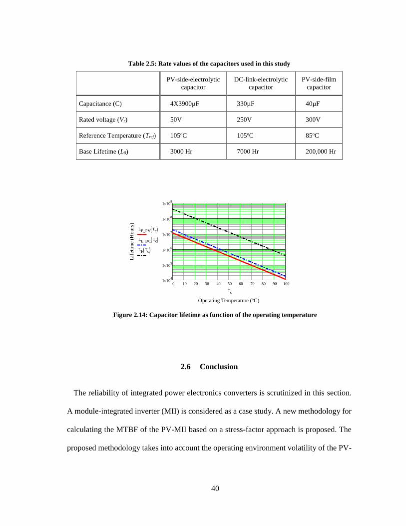
40
Table 2.5: Rate values of the capacitors used in this study
PV-side-electrolytic
capacitor
DC-link-electrolytic
capacitor
PV-side-film
capacitor
Capacitance (C) 4X3900µF 330µF 40µF
Rated voltage (Vr) 50V 250V 300V
Reference Temperature (Tref) 105oC 105oC 85oC
Base Lifetime (L0) 3000 Hr 7000 Hr 200,000 Hr
0 10 20 30 40 50 60 70 80 90 1001 10
4
1 105
1 106
1 107
1 108
1 109
Operating Temperature (°C)
Lif
etim
e (H
ou
rs)
LE_PV Tc
LE_DC Tc
LF Tc
Tc
Figure 2.14: Capacitor lifetime as function of the operating temperature
2.6 Conclusion
The reliability of integrated power electronics converters is scrutinized in this section.
A module-integrated inverter (MII) is considered as a case study. A new methodology for
calculating the MTBF of the PV-MII based on a stress-factor approach is proposed. The
proposed methodology takes into account the operating environment volatility of the PV-

41
MII. Hence, the results provide a quantified assessment of realistic MTBF under expected
operating conditions. The MTBF for six different MII topologies was calculated based on
the expected usage model for a PV module-integrated inverter and the MIL-HDBK-217.
It was found that considering the usage model, rather than a singular worst-case operating
point, yields a more optimistic MTBF. The results showed confirm the long-held belief
that the double-line frequency decoupling capacitor is the dominant component, not the
MOSFET, regardless of the numbers of power switches needed in the topology. Moreover,
topologies that employ film capacitor for power decoupling instead of aluminum
electrolytic capacitors have higher MTBF and longer lifetime. The reader is undoubtedly
aware that the computation of MTBF can be easily influenced by good and bad design
practices, such as component derating. Therefore, the objective of this study is not to judge
the reliability merits of one topology over another. Rather, it is meant to present a method
of applying a usage model of expected inverter operation as an evaluation tool when
comparing different topologies on the basis of MTBF. The dataset we used in this section
is, admittedly, limited, and therefore, it should not be taken to generally represent the
expected MII reliability in general. Further work in this area will apply a larger dataset of
operating points to represent a higher fidelity set of operating conditions.

42
3 MICROINVERTER AND STRING INVERTER GRID-CONNECTED
PHOTOVOLTAIC SYSTEM – A SYSTEMATIC STUDY *
This section presents a systematic comparison between two different PV configurations:
a string inverter based PV energy system and a microinverter based system. Reliability,
environmental factors, inverter failure, and electrical safety of a test case 6kW residential
PV system are thoroughly evaluated and compared considering the two configurations.
The impact of all these features on the cost of the PV system is estimated. The results
show that when the levelized cost of energy (LCOE) is considered, the break-even cost
can be reached by the microinverter more quickly than with a string inverter operating in
the same environment. Moreover, considering the replacement cost associated with the
expected string inverter failure, the microinverter configuration is the more cost effective
configuration.
3.1 Introduction
Is a microinverter more expensive than a string inverter? A microinverter connected to
a single PV module has become a trend for residential grid-connected PV systems,
replacing a single inverter connected to a string of series-connected PV modules. This is
due microinverter advantages including: (1) improved energy harvest, (2) improved
* © 2013 IEEE. Reprinted, with permission, from S. Harb, M. Kedia, H. Zhang, and R.S. Balog,
“Microinverter and String Inverter Grid-connected Photovoltaic System—A Comprehensive study,” 39th
IEEE Photovoltaic Specialists Conference (PVSC), June, 2013.
43
system efficiency, (3) lower installation costs, (4) plug-N-play operation, and (5) enhanced
flexibility and modularity [8, 9, 47]. At first glance, the string inverter appears to have a
lower per-watt capital cost when just the inverter is considered. However, the inverter
represents only about 15% of the entire PV system cost whereas the installation labor and
balance of system (BOS) cost account for 40%, depending on the system configuration
and inverter technology [48]. These factors have made it difficult to perform a comparative
cost study. Hence, in this section, we consider a 6kW PV system and compare the
microinverter-based system with the string inverter-based system.
An alternating-current photovoltaic module (ACPV) is created when the microinverter
is directly attached to a single PV module [49-52]. The result is a PV module that produces
AC power without any extra electronic components. The implication, however, is that
since the power electronic is indelibly integrated with the PV module, the microinverter
must have a lifetime that matches the lifetime of the PV module—namely 25 years. Hence,
most of the microinverter manufacturers provide a standard 25-year warranty [49, 50, 53,
54]. The high-reliability and long lifetime of the microinverter offer an added advantage
over the string inverter that typically has a lifetime of only 10 years [55]. The impacts of
the longer lifetime on the power generation, system failure, maintenance, and replacement
cost have not been thoroughly investigated in the literature. This section identifies the
effects of all the aforementioned factors on the total cost of the system over the expected
25-year lifetime of the PV module.
This section is organized as follows: the specifications of the system considered in this
study are presented in the next section. Then, the reliability impacts of both configurations
44
are evaluated. After that, the impact of the operating environment is presented, and the
levelized cost of energy (LCOE) of the system is evaluated. Finally, although it is not easy
to quantify because of limited published data, the safety of the microinverter versus string
inverter configurations is considered.
3.2 Case study system characteristics
In order to have an apple-to-apple comparison, a 6kW grid connected PV system is
designed considering two approaches. The first approach uses a string inverter
configuration, with 24 PV modules—250W each. Two strings are formed and connected
in parallel; each string consists of 12 PV modules in series. Then, the DC output is
connected to a 6kW string inverter, as shown in Figure 3.1(a). The other PV system is
based on the microinverter concept in which each PV module is connected to one
microinverter. The 24 microinverters are connected in parallel (AC connection), as shown
in Figure 3.1(b). The safety of the high DC string voltage connection versus the AC
connection will be examined later in this section.
The purpose of this study is not to evaluate the performance of the inverter itself, but
rather the impact of different inverter-module configurations on the overall performance,
lifetime and cost of the PV system. Therefore, the following features are assumed to be
common for both string inverter and microinverter: (1) efficiency, (2) high quality voltage
and current output, and (3) galvanic isolation. Also, both inverters are equipped with the
maximum power point tracking (MPPT) feature [56] in order to harvest the maximum
available energy. The string inverter performs MPPT at the string level while in the

45
microinverter configuration MPPT is performed at the module level. This leads to an
increase in the amount of harvested energy and reduce the effect of shaded modules [8,
57, 58]. The impact of shaded module is quantitatively evaluated later in this study.
Recently, the DC/DC optimizer has been proposed mainly to overcome the mismatch
between the different PV modules and enhancing the energy harvesting function with a
module-level MPPT [59, 60]. However, this configuration still suffers from the single
point failure problem since only one DC/AC inverter is used for the whole system.
Moreover, the DC/DC optimizers are connected in series to form high DC voltage that is
fed into the string inverter. Hence, it is not considered in this study.
Monitoring the performance of the system is an essential feature for any PV system; it
helps monitoring the power generation as well as detecting any failure the moment it
happens that expedites the repair time. Consequently, it is assumed that both systems are
equipped with a device that continuously monitors the system performance [55, 61].
Figure 3.1: Comparison of electrical wiring for photovoltaic systems: (a) series dc connection
for the string inverter (b) parallel ac connection for the microinverter
(a) (b)
DC
AC
Grid
High Voltage DC
DC
DC
DCA
C
AC
AC
Grid
AC Connection

46
3.3 Reliability of the PV system
Currently, microinverter manufacturers are providing 25-year warranties [49, 50, 54].
On the other hand, manufacturers of string inverters typically provide 10 years warranties,
and thus, the string invert is expected to need replacement at least once over the 25 years
power-output guaranty of the PV modules [55, 62]. Thus the total system lifetime cost of
the string inverter must include two inverters, the original and a replacement.
The inverter is generally considered to be the most failure prone component in the PV
energy system [55, 63]. Recently, some PV operators have started publishing failure data
from their installed PV systems. These results show that the string inverter is responsible
for 43% of failures and 36% of energy loss [63]. The similar data for the microinverter is
not available because it has not been in the field for long time yet. However, in addition
to the 25-year warranty, its mean time to fail (MTTF) is very high, around 300 years [53].
This means that the probability of the microinverter to accomplish all the required tasks
with no failure, during the useful lifetime, is 92% [33]. However, similar information is
not available for the string inverter. Hence, the failure rate of the conventional string
inverter is calculated in this study using MIL-217 handbook and the analysis in [47]. In
single-phase inverters, energy storage, usually capacitors, is needed for double-frequency
power decoupling. If the capacitor is located on the DC bus inside the inverter, the required
capacitance is a function of the power ratings, DC voltage bus voltage, allowable bus
voltage ripple, and the grid frequency [8, 64]:

47
VDC
V
PVP
DC
0
(3.1)
Equation (3.1) shows that the required capacitance is directly proportional to the
system’s power rating. Since the string inverter is rated for high power (6kW), it uses a
large electrolytic capacitor as an energy balancing device [8, 9, 64]. It is known that
electrolytic capacitors are the weakest component in the inverter [47]. Its failure rate, given
in (3.2), is directly proportional to its capacitance and operating voltage and temperature
[31]. This suggests that the failure rate of the string inverter is expected to be higher than
the failure rate of the microinverter:
EQCVCbn
CP
_*
_
5
378
27309.5exp1
3
5.000254.0
_mTS
Cb
18.034.0 CCV
10Q
(3.2)
For the 6kW PV system at 400VDC and 2% (8V) ripple, a 5,000µF is required as a
decoupling capacitance according to (3.1). In practice, inverter manufacturers de-rate the

48
decoupling capacitance in order to ensure sure that the minimum capacitance requirement
is met at the end of the inverter’s lifetime. Assuming a stress factor (S) of 0.75, and 50°C
operating temperature, the failure rate of a conventional string inverter is calculated using
(3.2) to be 1.5 failures per million hours. This can be interpreted, using (3.3), as 72%
probability of operation and accomplishing all the required functions during its expected
lifetime (25 years); whereas a commercial microinverter has a 92% probability.
tep (3.3)
Unlike the conventional energy generating source, the loss (or cost) is related only to
the cost of repair, since when the system is down no fuel is being consumed. But, in the
case of alternative energy resource in general and PV system especially, the time that the
system is not operating is considered as loss. This is because the energy source (or the
fuel) is free, and just needs to be converted to the useful form. Hence, this potential energy
loss is a key factor that should be precisely evaluated to help estimate the levelized cost
of energy (LCOE) over the expected lifetime of the system. The impact of the failure rate
manifests itself in the amount of loss in energy production when the inverter is not
operating due to failure or repair time. However, a typical residential 6KW string inverter
is non-repairable; rather it will be replaced with a new inverter once it fails. The cost of
the inverter depends on whether the manufacturer warranty is limited to only one
replacement during the inverter’s lifetime. In this study we assume that the warranty is for
49
unlimited replacement during the inverter’s lifetime and that the inverter will be replaced
only one extra time during the PV system’s lifetime (25 years) not covered by the
warranty. The quantified cost will be presented later in the cost section.
3.4 Environmental impact
In this section, the impact of shaded PV modules is examined. It is expected that with
different insolation level, the energy production, from PV modules of a fixed capacity also
changes. The insolation dataset used is the average of the insolation level over the last 22
years for Austin, TX [65]. Consequently, the total expected energy production, over the
PV modules’ lifetime, is 1,660,324 kWh. Next, the loss of energy production due to the
shade of PV modules is investigated. In string inverter configuration, multiple PV modules
are connected in series. Thus, even if only one PV module is shaded, the power output of
the entire string is reduced. In the microinverter configuration, because MPPT is
performed at the module level, the loss due to shading of only one module does not affect
the output of the unaffected modules. In a case study of 6kWh PV system at Austin, TX,
the effect of 50% and 100% shading of one module is shown in Figure 3.2 and Figure 3.3.
Evaluating the exact cost of the loss of energy production due to shading effects is very
complicated because the shading depends on many factors that vary by location,
surrounding environment, time of day, and season of the year.
However, the probability of shading can be calculated for a specific location, and thus,
the expected loss of energy production is calculated. In [57], a comparison study between
a string inverter and microinverter PV systems was conducted that is intended to analyze
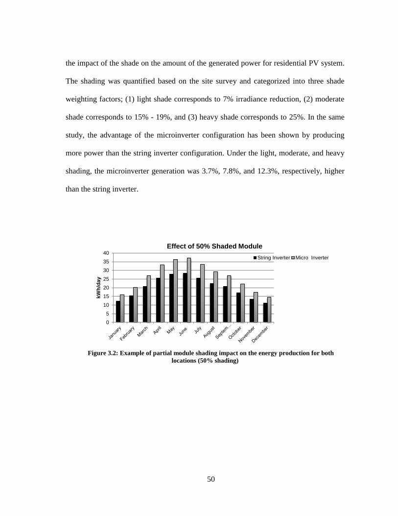
50
the impact of the shade on the amount of the generated power for residential PV system.
The shading was quantified based on the site survey and categorized into three shade
weighting factors; (1) light shade corresponds to 7% irradiance reduction, (2) moderate
shade corresponds to 15% - 19%, and (3) heavy shade corresponds to 25%. In the same
study, the advantage of the microinverter configuration has been shown by producing
more power than the string inverter configuration. Under the light, moderate, and heavy
shading, the microinverter generation was 3.7%, 7.8%, and 12.3%, respectively, higher
than the string inverter.
Figure 3.2: Example of partial module shading impact on the energy production for both
locations (50% shading)
0
5
10
15
20
25
30
35
40
kW
h/d
ay
Effect of 50% Shaded Module
String Inverter Micro Inverter

51
Figure 3.3: Example of complete module shading impact on the energy production for both
locations (100% shading)
In this section, we present an approach to quantify the cost of the loss of energy
production due to the shade effects. Similarly, shade site survey can be used to determine
the shade weighting factors for a specific installation. However, the results from [57] will
serve the purpose of the study in this paper, and thus, they are used to calculate the loss in
energy production. First, the expected energy generated by the microinverter configuration
will be calculated using the irradiance reduction percentage (r) [57]:
T
ErSHmicro
E 1_ (3.4)
where: r = 7%, 19%, and 25%. This energy will be considered the reference value against
which the energy produced by the string inverter is compared. The energy generated by
0
5
10
15
20
25
30
35
40
kW
h/d
ay
Effect of 100% Shaded Module
String Inverter Micro Inverter

52
the string inverter will be less than from the microinverter by the gain factor k [57],
SHmicro
EkSHstring
E_
1_
(3.5)
where k = 3.7%, 7.8%, and 12.3%.
The gain in energy produced by the microinverter is calculated as
microshkE
stringshE
microshEgainE
___ (3.6)
Table 3.1 summarizes the results for three shade weighting factors.
Table 3.1: The impact of the shade on the gnerated energy
Shade weighting
factor
Microinverter
energy (kWh)
String inverter
energy (kWh)
Energy Gain of microinverter
system (kWh)
Light
1,544,101 1,486,970 57,131
Moderate
1,344,862 1,239,963 104,899
Heavy
1,245,243 1,092,078 153,165

53
3.5 Cost
The cost of the PV system can be divided into the following categories: PV module,
inverter, balance of system (BOS), installation, maintenance and repair, and lost
production costs [55, 63]. Apart from the cost of the PV modules, the cost of other factors
differs based on the configuration that is selected to configure the system. String inverter
and microinverter configuration s are evaluated considering the aforementioned factors.
The total cost of installed residential PV system, in US, is $4.36 /watt, with only $1.8/watt
cost for PV module. The large difference in the cost is mainly due to the expensive labor
in US [48]. The installation process for the string inverter needs a high level of electrical
skills, because of the nature of the system that involves different subsystems that need to
be connected together at high DC voltage, such as high voltage DC wiring, string combiner
box, and DC protection circuit. On the other hand, in the microinverter configuration, the
AC outputs of the inverters are connected in parallel, which is easy, safer, and needs
shorter installation time. The study in [66] shows that the microinverter saves 24% of
installation cost, and 11% of the system cost for 7kWH system. Moreover, the total cost
of the maintenance, as a percentage of initial PV system costs, is 11% for string inverter,
and only 2% for the microinverter [66]. Table 3.2 lists the BOS for each configuration
along with the available retailer prices. It is worth to mention that these are the retailer
prices, since it is hard to estimate the real cost.

54
Table 3.2: BOS retailer prices for both approaches
String Inverter Microinverter
Components Cost ($/Unit) Components Cost
($/Unit)
Fuse PV-10A10F (DC) $17.21 Cable (1986164-2 TYCO) $1.01
(per foot)
Fuse PV-20A10F (DC) $27.14 Transition Cable $47.00
Fuse Holder (CHPV1U) $19.64 End Caps $2.50
Blocking Diode (SD 2510-B) $15.00 Data Logger $627.50
DC Disconnects (SBCD-4-40) $260.16 Transition Box (2106916-1
TYCO) $99.95
Cable (1986164-2 TYCO) $1.01
(per foot)
AC Disconnects
(H321DSEI) $2,382.39
Cable Coupler (6-1394462-3-
female; 6-1394461-5-male
TYCO)
$2.32
Cable Coupler (6-1394462-
3-female; 6-1394461-5-male
TYCO)
$2.32
Sub-array Combiner Box (SPD) $322.35
AC Disconnects (H321DSEI) $2,382.39
Data Logger $627.5
Total $4,035.34 Total $3,400.09
To refine the cost estimate from the installer side, two quotations were obtained from
Austin, TX based PV installers, for both configurations [67], as shown in Table 3.3. The
microinverter configuration costs just $581.4 extra than the string inverter configuration.
This extra cost can be easily compensated when the cost of loss of energy production is
taken in consideration. Table 3.3 shows that the labor cost is the same for both approaches;
nevertheless, few microinverter manufacturers have started producing what so called
“ACPV” to reduce the installation cost to half [49, 50, 54]. In the ACPV, the microinverter
is physically and electrically connected to the PV module in the factory.

55
Table 3.3: PV installer quotations
Total cost PV modules, inverter, and BOS Labor
Microinverter approach 20,359.72 16,265.40 3,190.00
String inverter approach 19,747.18 15,684.00 3,190.00
3.5.1 Levelized cost of energy (LCOE)
The aforementioned quotations are the cost of the installed PV system, however,
levelized cost of energy (LCOE) is not considered. These quotations do not include the
cost of unharnessed energy due to system’s failure and shading effects. In order to
comprehensively evaluate the cost as well as calculate the break-even cost of the PV
system, the LCOE needs to be calculated.
The calculation of the loss of energy production, due to system failure, can be divided
into two main time factors: time to detect the failure and the time to repair. In the string
inverter case, failures that are not related to the inverter can be easily missed, and the
system continues to operate at lower power rating. In a system similar to the string system
studied in this paper [68], a connector failure in one of the two strings resulted in a
reduction of the harvested power to half of the expected value. This failure persisted for
two months during the summer of 2012 until it was accidently discovered. Also, the repair
time is very complicated to expect, it depends on the cause of failure, whether it is
hardware or software failure [63]. Hence, the string inverter is considered to be replaced
at least one time during the 25 years PV system’s lifetime.

56
On the other hand, the cost of the loss of energy production due to shade effects can be
calculated using the results presented in the previous section. Using the price of electricity
in Austin, 0.109 $/kWh, the energy production gained by the microinverter is interpreted
into cost for the three shade weighting factors, light, moderate, and heavy, as follows:
$6,227, $11,434, and $16,695, respectively. If these gains are evenly distributed over the
system’s lifetime, then, it will be $249, $457, and $668. Since the difference between the
two quotations is $581, this concludes that microinverter configuration PV system takes
at most, considering light shade weighting factor, less than three years to reach the break-
even cost with the string inverter configuration. It is worth to mention that the replacement
cost of the string inverter has not included in the previous calculations. An average price
for a 6kW string inverter is approximately $2,500. Adding this $2,500 as a replacement
cost, results in making the microinverter configuration cost competitive with the string
inverter at the time of installation. Another way to calculate the break-even cost is to
compare the cost of the power electronics. 24 microinverters are needed to construct a
6kW PV system with $130/piece retailer price; the total is $3,120. Again, $620 will be the
difference in favor of the string inverter, which will be compensated by the gain in energy
harvest by the microinverter.
3.6 Safety
Safety of PV systems is becoming increasingly a concern [69, 70]. This paper compares
the safety of both the string inverter and the microinverter configurations. The safety
aspect of the PV system is very crucial not only because of the hazardous conditions that

57
could result, but also because of the potential for large financial losses. The latter can be
interpreted into cost (LCOE); however, due to the lack of research in this particular topic,
it is complicated to quantify the cost caused by hazardous conditions. The safety has been
studied in two aspects; (1) shock hazard and (2) arc fault.
Shock hazard is related to the amount of the current flow, which depending on the
voltage level, and can be lethal. In the string inverter configuration, the DC voltage can be
as high as 600VDC, creating a hazardous system voltage [71]. On the other hand, the DC
voltage level in the microinverter configuration is limited to the output of the PV module,
which could be as high as 40VDC. Moreover, this DC voltage is connected to the
microinverter either directly or by very short wires, and thus, the potential for a hazardous
situation is much less. Arc faults are more likely to occur in high DC-voltage PV
connection system, and can cause system fires [70]. Figure 3.4 [72] and Figure 3.5 [73]
show examples of hazards and resulting damage from arcing in PV systems.

58
Figure 3.4: Glowing arc in the DC wiring near a combiner box [72]
Figure 3.5: Fire damage to a roof-mounted PV array [73]

59
Three aspects of system design contribute to the arc faults risk: high voltage, high
current and large geographic distribution of AC or DC wiring. Arc faults can be divided
into AC and DC arc faults based on the electrical connection. However, AC connections
are less likely to sustain arcs since the current flows through zero twice per grid cycle [71].
In the string inverter configuration based PV system, 12 PV modules are connected in
series to form 360VDC. Then, connecting multiple strings in parallel will increase the DC
current. Besides, these PV modules with the DC distributed connection occupy a large
geographic area. This combination of high voltage, high current and large DC distributed
area results in increasing the probability of an arc fault to occur. Figure 3.6 illustrates
possible locations for arc faults in a typical string inverter configuration PV system [70].
Figure 3.6: Possible arc faults locations in string inverter

60
Standards have been developed to address the safety issues in PV system, for example:
UL1699B photovoltaic arc-fault circuit protection standard, which is a subset of the
National Electrical Code (NEC 690). It defines requirements for systems with a DC bus
voltage equal to or greater than 80 VDC and less than 1,000 VDC [70]. These standards
necessitate installing necessary protection equipment to ensure the safety of the system.
Hence, this leads to increase the total cost and the complexity of whole system.
In contrast, the microinverter configuration works at much lower DC voltages; the PV
module output voltage of 18V to 36V for most silicon modules. With this lower DC
voltage, it is harder to sustain an arc [74]. Moreover, the microinverter is physically
attached to the back of the PV module, thus, the DC wiring is almost negligible.
Microinverters are designed to stop operating once a fault or disconnection in the wiring
is detected. However, quantifying the cost associated with the extra safety requirements is
difficult due to two main reasons: (1) the safety of PV system is new topic, and has not
been thoroughly studied yet; (2) the protection equipment technology is still immature and
different technologies have been proposed recently.
3.7 Conclusion
Two different power electronics configurations for PV system, string inverter and
microinverter, are examined and compared in this paper. Reliability, availability, safety,
failure, and cost of both configurations were compared. The additional energy harvest of
the microinverter was found to give it an economic advantage over the expected lifetime
of the PV system, particularly when the cost of replacing the string inverter is taken into

61
account. The microinverter also offers safety advantages, which have not previously been
monetized into the LCOE calculations.
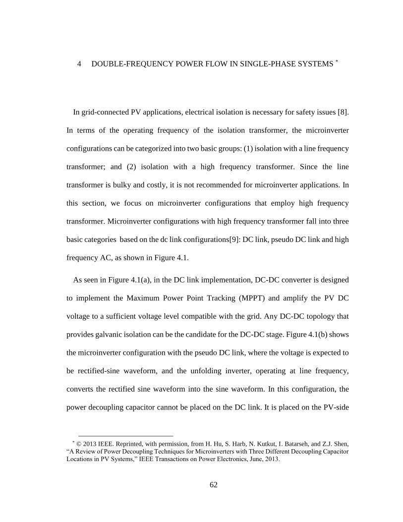
62
4 DOUBLE-FREQUENCY POWER FLOW IN SINGLE-PHASE SYSTEMS *
In grid-connected PV applications, electrical isolation is necessary for safety issues [8].
In terms of the operating frequency of the isolation transformer, the microinverter
configurations can be categorized into two basic groups: (1) isolation with a line frequency
transformer; and (2) isolation with a high frequency transformer. Since the line
transformer is bulky and costly, it is not recommended for microinverter applications. In
this section, we focus on microinverter configurations that employ high frequency
transformer. Microinverter configurations with high frequency transformer fall into three
basic categories based on the dc link configurations[9]: DC link, pseudo DC link and high
frequency AC, as shown in Figure 4.1.
As seen in Figure 4.1(a), in the DC link implementation, DC-DC converter is designed
to implement the Maximum Power Point Tracking (MPPT) and amplify the PV DC
voltage to a sufficient voltage level compatible with the grid. Any DC-DC topology that
provides galvanic isolation can be the candidate for the DC-DC stage. Figure 4.1(b) shows
the microinverter configuration with the pseudo DC link, where the voltage is expected to
be rectified-sine waveform, and the unfolding inverter, operating at line frequency,
converts the rectified sine waveform into the sine waveform. In this configuration, the
power decoupling capacitor cannot be placed on the DC link. It is placed on the PV-side
* © 2013 IEEE. Reprinted, with permission, from H. Hu, S. Harb, N. Kutkut, I. Batarseh, and Z.J. Shen,
“A Review of Power Decoupling Techniques for Microinverters with Three Different Decoupling Capacitor
Locations in PV Systems,” IEEE Transactions on Power Electronics, June, 2013.

63
instead, and usually this results in a large capacitance due to the low DC level and the need
for ripple-free voltage on the PV-side.
If we replace the rectifier circuit on the secondary side with the cyclone converter, a
new configuration without the DC link is derived, as illustrated in Figure 4.1(c). In this
case, the cyclone converter directly converts the high frequency AC into the desired line
frequency AC output. As for the power decoupling capacitor, in this case usually it is
placed on the PV-side, which is similar to the previous case, and a large capacitance is
needed. However, the power decoupling capacitor can be placed on the AC side, and
consequently, a very small capacitance is needed for the same power ratings.
Figure 4.1: Basic microinverter’s configurations
High
frequency
isolation
DC link
Pseudo DC link
Without DC link
(High frequency AC)
DC/ACRectifier
Decoupling
capacitor
High
frequency
transformer
DC/DC converter
UnfolderRectifier
Decoupling
capacitor
High
frequency
transformer
DC/DC converter
Cyclone
converter
Decoupling
capacitor
High frequency
DC/AC
Alternative
decoupling
capacitor
(a)
(b)
(c)
CD
CD
Grid
Grid
Grid
High
frequency
transformer
CD
CD

64
This section presents the double-line frequency issue that is inherent in the single-phase
conversion systems. Also, it scrutinizes the various power decoupling techniques that have
been proposed and compares their performance in terms of efficiency, cost, and control
complexity. Although the following analysis is based on the single-phase, grid-connected
PV system, shown in Figure 4.2, but the result or the effect is similar for a single-phase
rectifier system.
Figure 4.2: Single-phase grid-connected PV system
4.1 Double-line frequency ripple
In a single-phase, grid-connected system, the injected current to the grid is given in (4.1)
and the grid voltage is given in (4.2).
Cin
DC/AC converter
PV Module
Grid
vg(t)
ig(t)

65
tg
Itg
i 0sin)( (4.1)
tgVtgv 0sin)( (4.2)
where ω0 is the grid frequency and 𝜑 is the phase difference between the injected current
and the grid voltage, which is desired to be zero for unity power factor operation. Then,
the instantaneous output power, p0(t), is given as follows:
)(*)()(0
tg
itg
vtp
(4.3)
tg
Ig
Vg
Ig
Vtp0
2cos2
1cos
2
1)(
0 (4.4)
when the phase shift (φ) is zero, then the expression for p0(t) in (4.4) is reduced to (4.5)
tg
Ig
Vg
Ig
Vtp0
2cos2
1
2
1)(
0 (4.5)
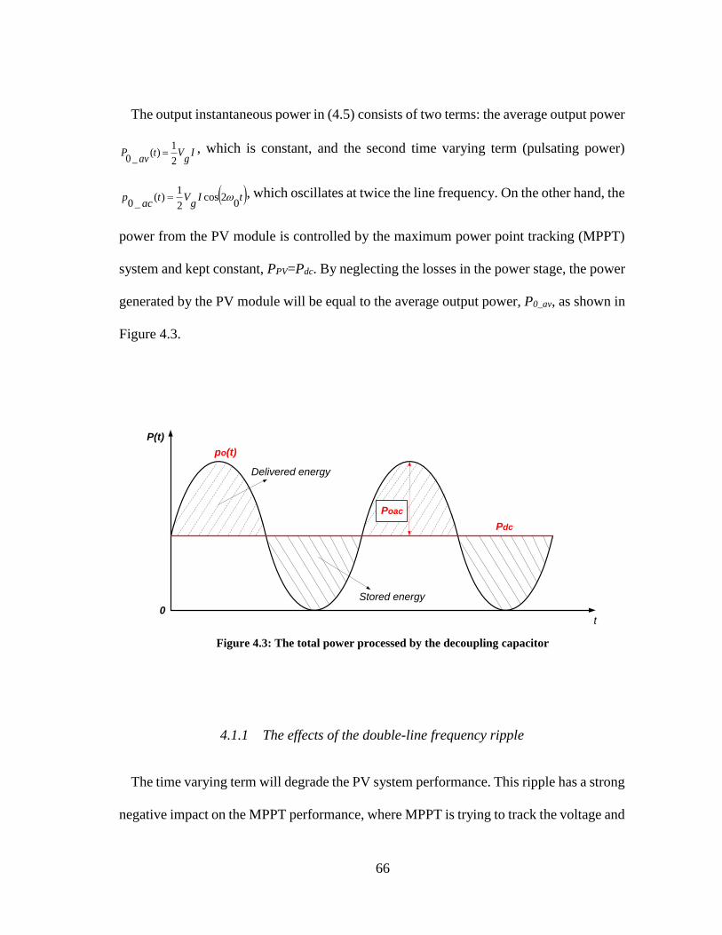
66
The output instantaneous power in (4.5) consists of two terms: the average output power
Ig
Vtav
P2
1)(
_0 , which is constant, and the second time varying term (pulsating power)
tIg
Vtac
p0
2cos2
1)(
_0 , which oscillates at twice the line frequency. On the other hand, the
power from the PV module is controlled by the maximum power point tracking (MPPT)
system and kept constant, PPV=Pdc. By neglecting the losses in the power stage, the power
generated by the PV module will be equal to the average output power, P0_av, as shown in
Figure 4.3.
Figure 4.3: The total power processed by the decoupling capacitor
4.1.1 The effects of the double-line frequency ripple
The time varying term will degrade the PV system performance. This ripple has a strong
negative impact on the MPPT performance, where MPPT is trying to track the voltage and
Delivered energy
Stored energy
po(t)
Pdc
t
P(t)
0
Poac
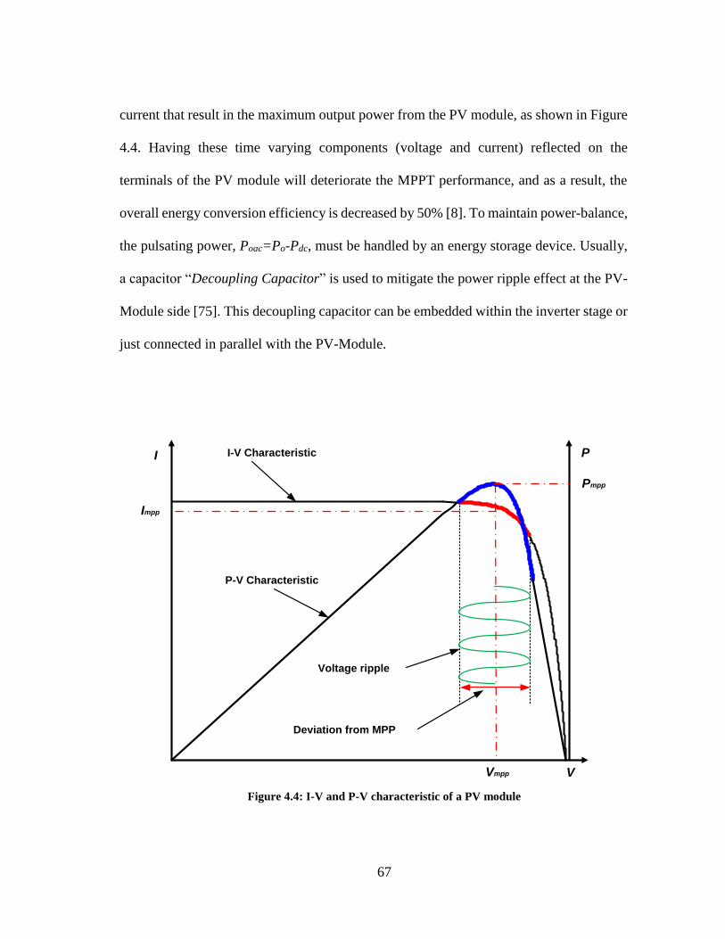
67
current that result in the maximum output power from the PV module, as shown in Figure
4.4. Having these time varying components (voltage and current) reflected on the
terminals of the PV module will deteriorate the MPPT performance, and as a result, the
overall energy conversion efficiency is decreased by 50% [8]. To maintain power-balance,
the pulsating power, Poac=Po-Pdc, must be handled by an energy storage device. Usually,
a capacitor “Decoupling Capacitor” is used to mitigate the power ripple effect at the PV-
Module side [75]. This decoupling capacitor can be embedded within the inverter stage or
just connected in parallel with the PV-Module.
Figure 4.4: I-V and P-V characteristic of a PV module
Voltage ripple
Deviation from MPP
V
I
Impp
P-V Characteristic
I-V Characteristic
Pmpp
P
Vmpp

68
The energy that is being charged to or discharged from the decoupling capacitor during
a half line cycle can be calculated by integrating one of shadowed areas in Figure 4.3.
)(2
1)))(((2 2
min_
2
max_8
1
0dcdcD
fodcCD VVCdttPPE grid (4.6)
where f0 is the line (grid) frequency, and Vdc_max and Vdc_min are maximum and minimum
voltages across the decoupling capacitor.
Combining (4.5) and (4.6), the required decoupling capacitance is found to be as
follows:
vdc
Vf
dcP
C
02
(4.7)
where Vdc is the DC voltage level and Δv is the allowed voltage ripple across the
capacitor’s terminals. It is obvious that by increasing either Vdc or Δv or both, the needed
decupling capacitance, to cancel the double-line frequency, decreases. However, this will
impose a higher voltage stress on the semiconductors, and thus, a compromise design
should be carried out.

69
Usually, a capacitor is used to serve as a power decoupling element. However, the
lifetime of different types of capacitors varies greatly, e.g. electrolytic capacitors typically
have a limited lifetime, namely 1000~7000 hours at 105˚C operating temperature [45].
Most of presently available commercial microinverter s use electrolytic capacitors as
power decoupling storage element due to their large capacitance and ease of
implementation, which tend to limit the lifetime of the microinverter [11, 53, 76, 77].
Some researchers have explored various ways to reduce the size of the required
capacitance so as to allow for other longer lifetime capacitor technologies, such as film
capacitors, to be used. In the next section, different power decoupling techniques are
presented, categorized, and compared in terms of efficiency and performance.
4.2 Power decoupling techniques
Different topologies and techniques have been proposed in the last decade that tackle
the double-line frequency issue, and enhance the reliability of the single-phase converters.
These topologies and techniques are presented in this section, and they will be categorized
into three different categories based on the place of the decoupling capacitor. Advantages
and disadvantages of each of these topologies will be discussed as well.
Based on the micro inverter configuration that is being employed, different power
decoupling techniques can be implemented. As it was shown in the previous section,
microinverter topologies can be divided into three groups, according to the DC link
configurations. Usually, the pseudo DC link configurations are referred to as single-stage
inverters since the second stage is just unfold the rectified low-frequency DC signal; hence

70
it is called “unfolder”. And, the decoupling capacitor can only be placed on the DC side.
Other configurations are considered multi-stage inverters. The single stage inverters, as
shown in Figure 4.5, accomplish both tasks: boosting the input voltage, and sine or
rectified sine waveform modulation. In this case, the only way to employ the power
decoupling capacitor is to place it on the DC (PV) side.
Figure 4.5: Single stage inverter
Unfolder
DC
Rectified
AC
Decoupling
capacitor
CD Grid
vg(t)
PV Module
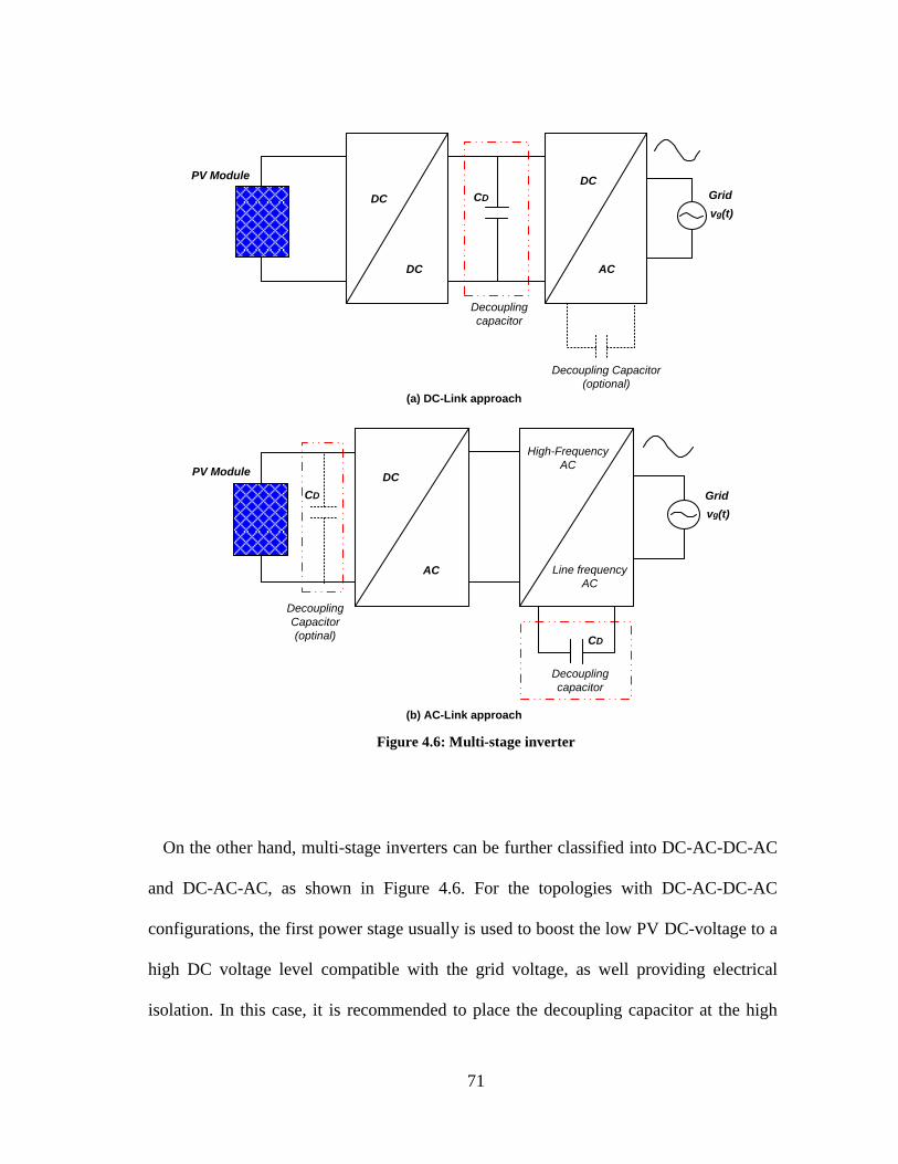
71
Figure 4.6: Multi-stage inverter
On the other hand, multi-stage inverters can be further classified into DC-AC-DC-AC
and DC-AC-AC, as shown in Figure 4.6. For the topologies with DC-AC-DC-AC
configurations, the first power stage usually is used to boost the low PV DC-voltage to a
high DC voltage level compatible with the grid voltage, as well providing electrical
isolation. In this case, it is recommended to place the decoupling capacitor at the high
DC
DC
Decoupling
capacitor
CD
DC
AC
Decoupling Capacitor
(optional)
PV Module
Grid
vg(t)
DC
AC
High-Frequency
AC
Line frequency
AC
Decoupling
Capacitor
(optinal)
Decoupling
capacitor
Grid
vg(t)
PV Module
CD
CD
(a) DC-Link approach
(b) AC-Link approach

72
voltage DC link, which will reduce the required decoupling capacitance, according to
(4.7). By adding several active switches and reactive components, the decoupling
capacitor can also be placed on the AC-side. Cycloconverters (or matrix) changing high
frequency AC to line frequency AC, are used in topologies with DC-AC-AC
implementation, in which the power decoupling capacitor can only be placed on the PV
side or on the AC side. Detailed description and analysis are given in the following
subsections. The inverter topologies can be categorized based on the location of the
decoupling capacitor and associated circuitry, as shown in Table 4.1. However, in this
study only the most three viable decoupling techniques options will be investigated,
namely, (1) PV side decoupling (IA1 and IB2); (2) DC link decoupling (IIA1); and (3) AC
side decoupling (IIIB2).
Table 4.1: Power decoupling techniques based on the place and the type of the capacitor
(Decoupling taxonomy)
Type – Decoupling Technique A- Electrolytic Capacitor B- Film Capacitor
Type I – PV side
1- Passive circuit Very Large capacitor
Low lifetime
Not cost effective
Very large capacitor
2- Active circuit Extra components – no
valuable improvement Extra components
Type II – DC-link
1- Passive circuit large capacitor
Low lifetime
Not cost effective
large capacitor
2- Active circuit Extra components – no
improvement Extra components
Type III – AC side
1- Passive circuit Not feasible Not feasible
2- Active circuit Not feasible
Extra components
Minimum required
capacitance
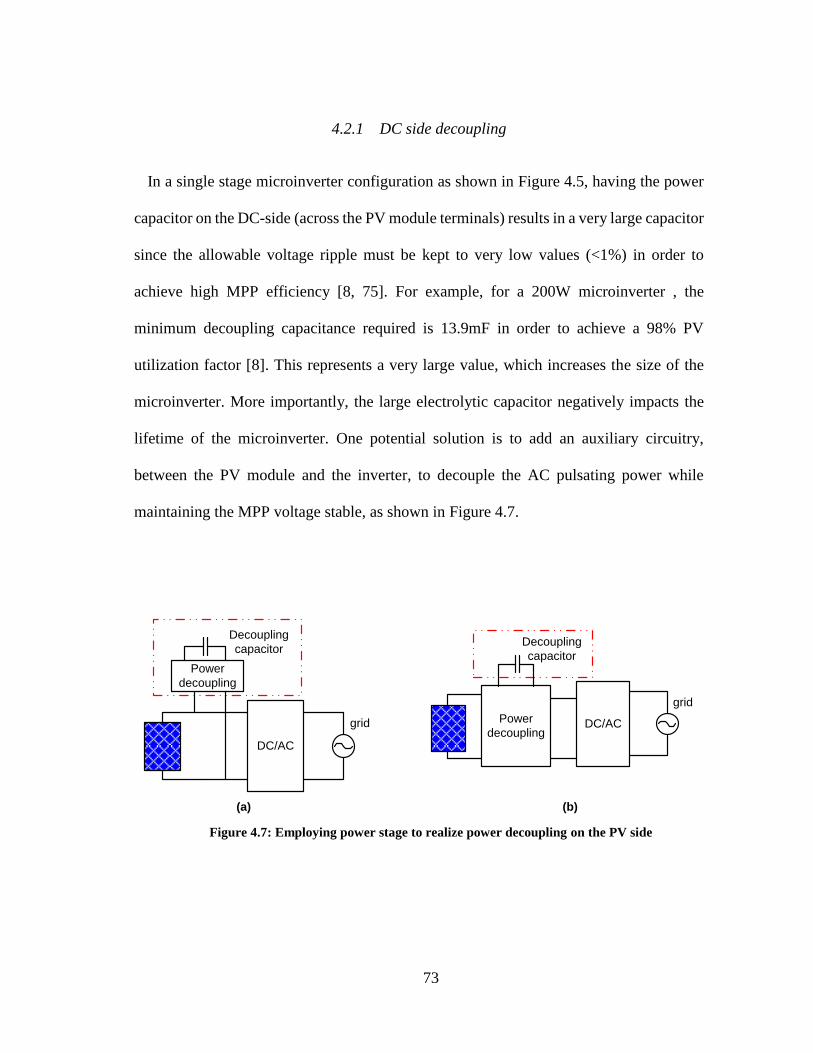
73
4.2.1 DC side decoupling
In a single stage microinverter configuration as shown in Figure 4.5, having the power
capacitor on the DC-side (across the PV module terminals) results in a very large capacitor
since the allowable voltage ripple must be kept to very low values (<1%) in order to
achieve high MPP efficiency [8, 75]. For example, for a 200W microinverter , the
minimum decoupling capacitance required is 13.9mF in order to achieve a 98% PV
utilization factor [8]. This represents a very large value, which increases the size of the
microinverter. More importantly, the large electrolytic capacitor negatively impacts the
lifetime of the microinverter. One potential solution is to add an auxiliary circuitry,
between the PV module and the inverter, to decouple the AC pulsating power while
maintaining the MPP voltage stable, as shown in Figure 4.7.
Figure 4.7: Employing power stage to realize power decoupling on the PV side
DC/AC
Power
decoupling
Decoupling
capacitor
grid DC/ACPower
decoupling
grid
Decoupling
capacitor
(a) (b)
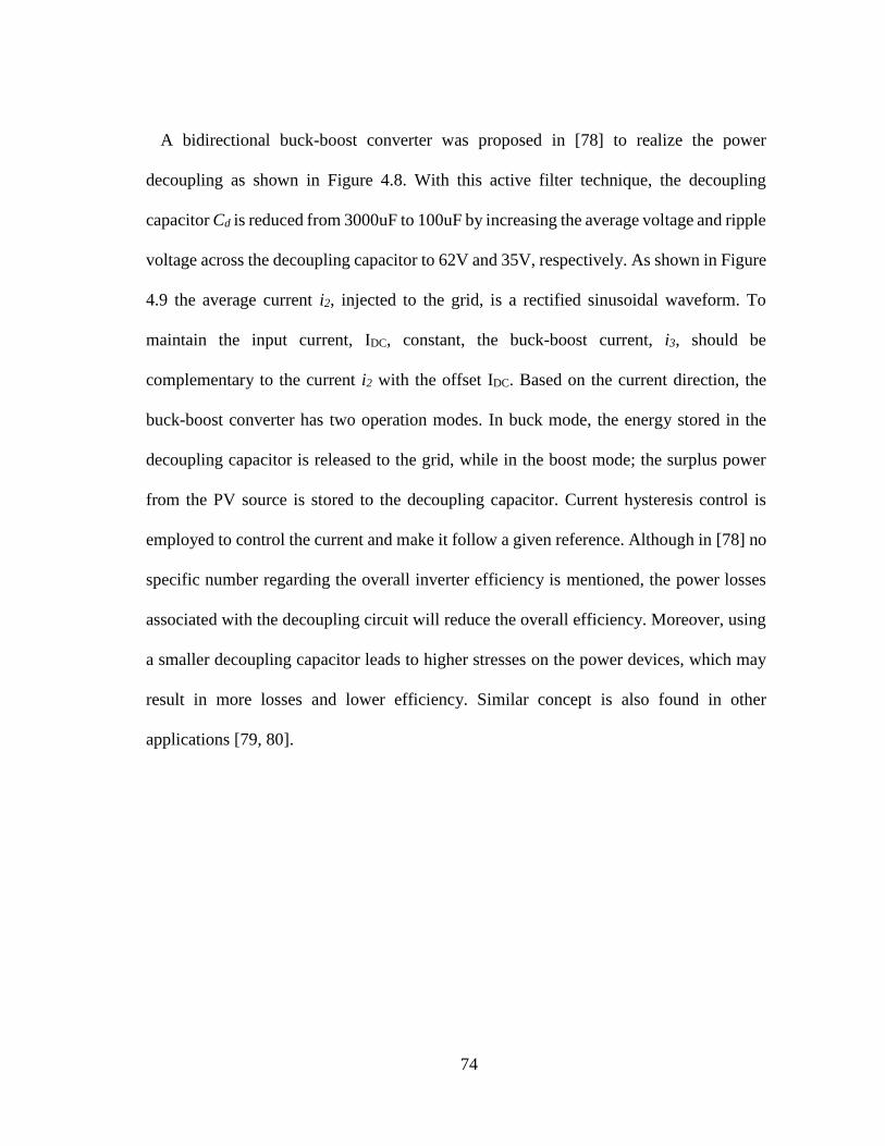
74
A bidirectional buck-boost converter was proposed in [78] to realize the power
decoupling as shown in Figure 4.8. With this active filter technique, the decoupling
capacitor Cd is reduced from 3000uF to 100uF by increasing the average voltage and ripple
voltage across the decoupling capacitor to 62V and 35V, respectively. As shown in Figure
4.9 the average current i2, injected to the grid, is a rectified sinusoidal waveform. To
maintain the input current, IDC, constant, the buck-boost current, i3, should be
complementary to the current i2 with the offset IDC. Based on the current direction, the
buck-boost converter has two operation modes. In buck mode, the energy stored in the
decoupling capacitor is released to the grid, while in the boost mode; the surplus power
from the PV source is stored to the decoupling capacitor. Current hysteresis control is
employed to control the current and make it follow a given reference. Although in [78] no
specific number regarding the overall inverter efficiency is mentioned, the power losses
associated with the decoupling circuit will reduce the overall efficiency. Moreover, using
a smaller decoupling capacitor leads to higher stresses on the power devices, which may
result in more losses and lower efficiency. Similar concept is also found in other
applications [79, 80].
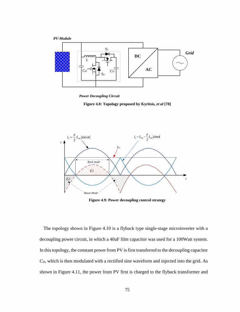
75
Figure 4.8: Topology proposed by Kyritsis, et al [78]
Figure 4.9: Power decoupling control strategy
The topology shown in Figure 4.10 is a flyback type single-stage microinverter with a
decoupling power circuit, in which a 40uF film capacitor was used for a 100Watt system.
In this topology, the constant power from PV is first transferred to the decoupling capacitor
CD, which is then modulated with a rectified sine waveform and injected into the grid. As
shown in Figure 4.11, the power from PV first is charged to the flyback transformer and
S1
S2
CD
L
Cdc
Power Decoupling Circuit
DC
AC
Grid
PV-Module
IDC
i
tIi DC
sin2
2 tIIi DCDC
sin2
3
t
E1
E2
Buck mode
Boost Mode

76
then is released to the decoupling capacitor, CD. After that, the energy stored in CD will be
injected to the grid in a sinusoidal form. Given the cascaded conversion process, the
projected efficiency will be low, as indicated in [44], where 70% is achieved as the peak
efficiency.
Figure 4.10: Topology proposed by Shimizu, et al [44]
Figure 4.11: Magnetizing currents at primary side
Cdc
Cf
Lf
Grid
D1
CD
S1
S2
S3
S4
D2
D3
Power Decoupling Circuit
PV-Module
i1
ix
T
1pi
1 xi i0
Charging magnetizing inductorReleasing to the
decoupling capacitor injected to the grid
ipx=Ix|sin(ωt)|

77
Figure 4.12 shows a modified topology in [39], where the leakage inductance energy is
recycled using a “dual-switch flyback converter”. As shown in Figure 4.13, the energy
from PV is stored in the magnetizing inductor by switching ON Ssync and SBB
simultaneously. Then the energy in the magnetizing inductor is discharged into the
decoupling capacitor through D1 and D2 once the switches Ssync and SBB turn OFF. When
the switches S1 and S2 turn ON at the same time, the decoupling capacitor, CD, discharges
the required amount of energy back into the magnetizing inductor, which will be injected
into the grid. Even with design optimization, the estimated peak efficiency is 86.7%
according to [39].
Figure 4.12: Modified topology proposed by Kjaer, et al [39]
CD
S2
Power Decoupling Circuit
Cf
LfS3
S4
D2
D3
S1D1
D4
PV-Module
Grid
Ssync
SBB
Cdc
1:N:N
iL
Lm

78
Figure 4.13: Key waveforms in one switching cycle
The authors in [37, 81] proposed three-port flyback topologies with one port dedicated
for the power decoupling function, as shown in Figure 4.14 and Figure 4.15. The power
decoupling capacitor (CD) serves both as an energy storage element and as a snubber to
recycle the leakage energy. For a 100W inverter, the decoupling capacitance can be as low
as 46uF with an average voltage 150V and 40V ripple across the decoupling capacitor.
The operation principle of these two topologies is quite the same, whose key waveforms
is illustrated in Figure 4.16, except that the peak magnetizing current in Figure 4.14 is
constant while in Figure 4.15, the peak value is constant in mode I and is variable in mode
II. These two topologies have two operation modes: In mode I, the input power is larger
than instantaneous output power, the surplus energy from PV is charged into CD. In mode
II, the input power is less than the instantaneous output power, the power from the CD
compensates the deficit power by switching ON the S2. By operating the converter in
DCM (Discontinuous Conduction Mode) mode, the peak efficiency can reach as high as
Ma
gn
etizin
g c
urr
en
t
iLm
iLm/N
AC switch curretn
SBB & Ssync
S1 & S2
S3 or S4

79
90.6%, including auxiliary power consumption [37].
Figure 4.14: Topology proposed by Hu, et. al [82]
Figure 4.15: Topology proposed by Harb, et. al [83]
S1
S2S3
S4D1
D2
D3
D4
D5
CD
Cdc
Lr
Cr
PV
Grid
n1
n1
n2
n2
Lm1
T1
Grid
S1
S2
D1
D2
S4
S3
D3
D4
T
Cf
Lf
Cdc
CDPV
Power decoupling
Port
1
Port 2
Port 3

80
Figure 4.16: Key waveforms for topologies in Figure 4.14 and 4.15
Figure 4.17 shows a novel microinverter with power decoupling capability, which is
composed of a push-pull type forward converter, an unfold inverter, and a decoupling
circuit depicted in a dotted-line area [84].For a 500W microinverter , the decoupling
capacitance (CX) is as small as 50uF in simulation with a voltage ripple, across its
terminals, around 100V. As shown in Figure 4.18, the topology has two operation modes.
In mode I, the surplus power is charged to the decoupling capacitor by turning ON the Sx0
and the switch Sm1 or Sm2 turns ON alternatively to inject the power into the grid. In mode
II, besides the power transfers from the PV source directly to the grid by turning ON the
Sm1 or Sm2, the decoupling capacitor (CX) also injects its energy, which was stored in mode
I, into the grid by turning ON the Sx1 or Sx2. The reported conversion efficiency is 95%
[84].
For Figure 4.15
For Figure 4.14

81
Figure 4.17: Topology proposed by Shinjo, et. al [84]
Figure 4.18: The driver signal for the topology in Figure 4.17
Another flyback-based microinverter is proposed in [85], as shown in Figure 4.19. A
Time-shared Magnetizing Modulation (TMM) method is employed to avoid double power
conversion, as illustrated in Figure 4.20. The operation principle is similar to the
topologies shown in Figure 4.14 and 4.15. The decoupling capacitor only stores surplus
power from the PV in mode I and releases the deficit power in Mode II, which results in
higher conversion efficiency in comparison to those in [39, 44]. Although the proposed
Cf
Lf
iDC
CDC
Power Decoupling
Circuit
SAC1
vDC
SM1
iAC
vAC
Ls
SM2
SX1
SX2
SX0vX CX
SAC2 SAC4
SAC3
LX
SM1
SM
2
Sx1
Sx2
Sx0
IAC*
IDC*
mode
ⅠmodeⅡ
carrier
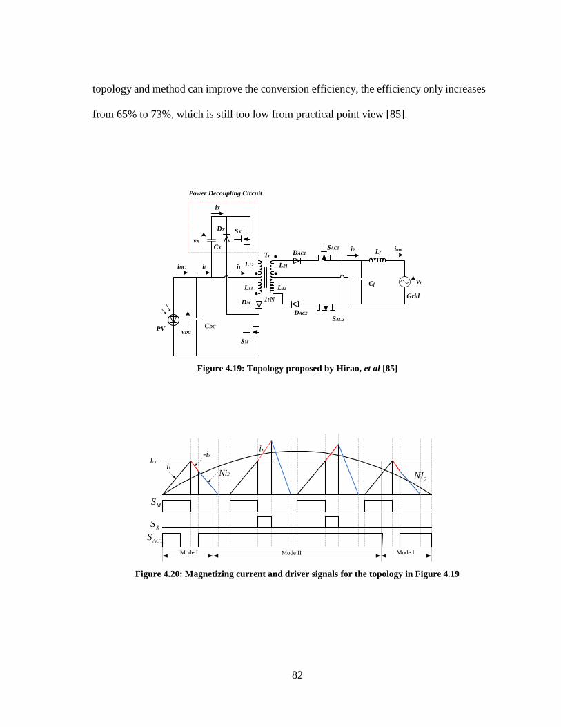
82
topology and method can improve the conversion efficiency, the efficiency only increases
from 65% to 73%, which is still too low from practical point view [85].
Figure 4.19: Topology proposed by Hirao, et al [85]
Figure 4.20: Magnetizing current and driver signals for the topology in Figure 4.19
Tr
Cf
Lf
Grid
DX SX
iDC
CDCPV
iX
Power Decoupling Circuit
ii i1
CX
L12 L21
L22L11
DAC1
SAC1
vDC
SM
DAC2
SAC2
i2 iout
vs
1:NDM
vX
MS
XS
1ACS
2NI
IDC
ii
-ix
ix
Ni2
Mode I Mode II Mode I

83
In [86], an additional winding and an active power decoupling circuit was added to the
conventional flyback converter, as shown in Figure 4.21. As shown in Figure 4.22, in
mode I, the surplus power from PV source is charged to the decoupling capacitor (C3)
through the third winding and two switches SM4 and SM6. In mode II, the energy stored in
C3 is delivered to the magnetizing inductor by turning ON SM5 and SM3, which will provide
the deficit power. Only 40µF decoupling capacitor is used for 200W microinverter system,
and the voltage ripple across C3 can reach as high as 100V [86]. In [87], a new flyback-
based microinverter is proposed, as shown in Figure 4.23, that uses a boost converter to
store the energy in the decoupling capacitor, (Cd) in one mode, and then release this energy
to magnetizing inductor through S2 during the other mode [87]. The operation modes are
illustrated in Figure 4.24. In Mode I, the power delivered to the grid is controlled by
turning ON S3, while the surplus power is charged to the decoupling capacitor by turning
ON S1. In mode II, after the switch S1 turns OFF, the magnetizing current continues to be
charged by switching ON S2 until the energy exactly equals the required energy by the AC
side.

84
Figure 4.21: Topology proposed by Chen, et. al [86]
Figure 4.22: Key waveform for topology in Figure 4.21
Figure 4.23: Topology proposed by Li, et. al [87]
VAC
IDC
VDC
C1
C2
C3
VC3
IM2
IMX
SM1
SM3 SM4
SM6 SM5
SM7 SM8
SM10 SM9
SM2D2
D3
Lm
N1 N2
T1
NX
LO
IAC
IM1
APDC Unfolder
IM1 IMX IM2
IM1p
SM1
SMx
SM2
Cin
Cf
LS
GridS1
S2
ip
SD
1:Ni1
PV PanelLd
CO
SAC1
Vpv
Cd
S3
SAC2
SAC3
SAC4

85
Figure 4.24: Operation modes and driving signals for the topology in Figure 4.23
In [88], the author combined the boost and flyback topologies and proposed a new
topology that is capable of implementing power decoupling with smaller capacitance, as
shown in Figure 4.25. The basic operation waveforms for the proposed topology are
shown in Figure 4.26. The energy stored in the decoupling capacitor (Cd) is delivered to
the grid through the forward converter when S2 turns ON. When S1 turns ON, the source
(VPV) charges the inductor (L1) and when the S1 turns OFF, this stored energy in L1 is
transferred to the decoupling capacitor. It can be viewed as a two-stage power conversion
with first stage for processing the DC power from PV, and the second stage for
implementing the AC power modulation. Using this technique, the size of the decoupling
capacitor will be reduced due to the relatively high voltage level and voltage ripple
allowed across its terminals.

86
Figure 4.25: Topology proposed by Tan, et. al [88]
Figure 4.26: Key waveforms for the topology in Figure 4.25
4.2.2 DC-link decoupling
For multi-stage microinverter design, the main power decoupling capacitor is placed on
the high voltage DC link, as shown in Figure 4.6(a). Unlike PV side decoupling, where
the PV nominal voltage is relatively low and the voltage ripple should be limited to a very
small range in order to maximize the energy harvest from the PV, DC link decoupling
allows for a higher DC link voltage as well as a higher voltage ripple voltage. Thus, this
leads to a smaller decoupling capacitance according to (4.7).
Although increasing the DC link level and voltage ripple leads to reduce the value of
Cr
Lr
grid
S3
S4
D4
D3
S1
S2
D1
D2
Cd
C1
L1
is1
S1
S2
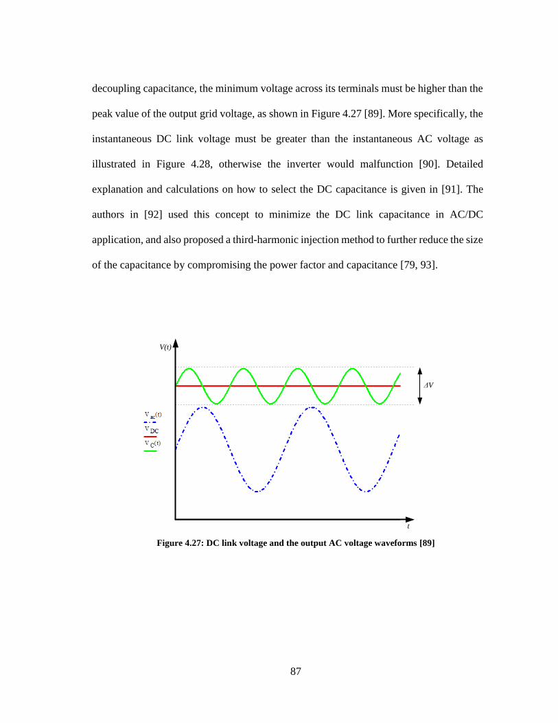
87
decoupling capacitance, the minimum voltage across its terminals must be higher than the
peak value of the output grid voltage, as shown in Figure 4.27 [89]. More specifically, the
instantaneous DC link voltage must be greater than the instantaneous AC voltage as
illustrated in Figure 4.28, otherwise the inverter would malfunction [90]. Detailed
explanation and calculations on how to select the DC capacitance is given in [91]. The
authors in [92] used this concept to minimize the DC link capacitance in AC/DC
application, and also proposed a third-harmonic injection method to further reduce the size
of the capacitance by compromising the power factor and capacitance [79, 93].
Figure 4.27: DC link voltage and the output AC voltage waveforms [89]
V(t)
t
ΔV

88
Figure 4.28: Allowed maximum DC voltage ripple [90]
Having a large voltage ripple across the DC link may result in deteriorating the output
current waveform. To resolve this issue, several control techniques have been proposed.
A simple method to mitigate the DC voltage ripple impact is to decouple the DC voltage,
as proposed in [94], in which a modified modulation strategy to reject the DC-link voltage
ripple in the control system is proposed. The proposed control scheme is illustrated in
Figure 4.29. In [95], a control technique is proposed, shown in Figure 4.30, that allows for
25% ripple voltage without distorting the output current waveform. In this design, the
voltage loop cutoff frequency was designed at 10Hz, greatly attenuating the double line
frequency DC voltage ripple in the control loop. However, with such low cutoff frequency,
the proposed control system degrades the system dynamic performance.
ms
(V)
DC voltage ripple
grid voltage
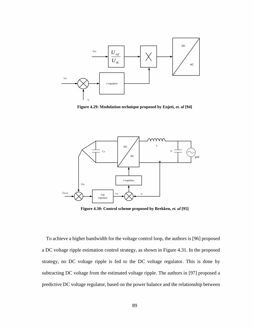
89
Figure 4.29: Modulation technique proposed by Enjeti, et. al [94]
Figure 4.30: Control scheme proposed by Brekken, et. al [95]
To achieve a higher bandwidth for the voltage control loop, the authors is [96] proposed
a DC voltage ripple estimation control strategy, as shown in Figure 4.31. In the proposed
strategy, no DC voltage ripple is fed to the DC voltage regulator. This is done by
subtracting DC voltage from the estimated voltage ripple. The authors in [97] proposed a
predictive DC voltage regulator, based on the power balance and the relationship between
Udc
dc
ref
U
U
DC
AC
i-regulator
io
iref
DC
AC grid
Cd
i-regulator
Udc
regulator
Udcref
Udc
iref io
L
C

90
energy and DC capacitor voltage, to achieve low current distortion on the AC side and
high voltage ripple on the DC link. The detailed design on how to maintain the constant
current draw from PV source and inject power into the grid with unity power factor, while
allowing the 25% DC voltage ripple of the rated DC link voltage is presented in [95]. In
this way, the DC voltage regulator can achieve a faster transient response. The authors in
[75, 98, 99] follow the same concept to allow the voltage ripple as large as possible, while
make the injected current acceptable in terms of THD.
Figure 4.31: Voltage-ripple estimation strategy for large DC ripple proposed by Ninad, et. al
[96]
4.2.3 AC side decoupling
In AC side decoupling techniques, the decoupling capacitor is usually embedded in the
inverter stage itself. Because of the high voltage swing on the AC side, the capacitor value
can be very small, and a non-polarized (film) capacitor can be used. In topologies that
DC
AC grid
Cd
i-regulator
Udc
regulator
Udcref
Udc
iref io
LC
Uripple
uo
Udcref
Ripple estimation
iref
io
uo
f
Uripple
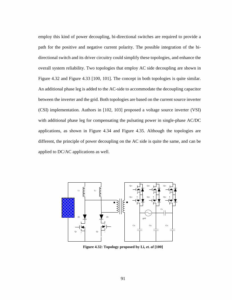
91
employ this kind of power decoupling, bi-directional switches are required to provide a
path for the positive and negative current polarity. The possible integration of the bi-
directional switch and its driver circuitry could simplify these topologies, and enhance the
overall system reliability. Two topologies that employ AC side decoupling are shown in
Figure 4.32 and Figure 4.33 [100, 101]. The concept in both topologies is quite similar.
An additional phase leg is added to the AC-side to accommodate the decoupling capacitor
between the inverter and the grid. Both topologies are based on the current source inverter
(CSI) implementation. Authors in [102, 103] proposed a voltage source inverter (VSI)
with additional phase leg for compensating the pulsating power in single-phase AC/DC
applications, as shown in Figure 4.34 and Figure 4.35. Although the topologies are
different, the principle of power decoupling on the AC side is quite the same, and can be
applied to DC/AC applications as well.
Figure 4.32: Topology proposed by Li, et. al [100]
D1D2
Q1 Q2
Q11
Q12
Q21
Q22
Q31
Q32
Ct1 Ct2 Ct3
L1 L2
Cb
grid

92
Figure 4.33: Topology proposed by Bush, et. al [101]
Figure 4.34: Topology proposed by Shimizu, et al [102]
idc
Sau Sbu Scu
Sal Sbl Scl
Cb Cf
Lf
grid
ia
ib
ic
Ldc
iAC
vAC C1
SW1
L1
SW2
SW3
SW4
SW5
SW6
CDC VDC
irip
U-Phase V-Phase W-Phase
RectifierCompensating Circuit
R
2
R
2
L2C2
vC1
iW
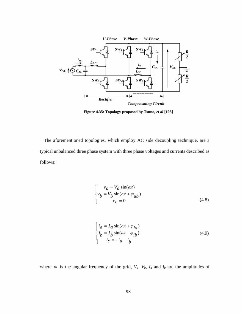
93
Figure 4.35: Topology proposed by Tsuno, et al [103]
The aforementioned topologies, which employ AC side decoupling technique, are a
typical unbalanced three phase system with three phase voltages and currents described as
follows:
0
)sin(
)sin(
cvub
tb
Vb
v
taVav
(4.8)
biaici
ibt
bI
bi
iataIai
)sin(
)sin(
(4.9)
where is the angular frequency of the grid, Va, Vb, Ia and Ib are the amplitudes of
iAC
vAC CAC
SW1
LAC
SW2
SW3
SW4
SW5
SW6
LW
iW CDC VDC
irip
U-Phase V-Phase W-Phase
RectifierCompensating Circuit
R
2
R
2

94
voltages and currents in phase a and b respectively. φvb is the voltage phase angle of phase
b, and φia and φib
are the current phase angles of phase a and b.
The total instantaneous power can be calculated as:
2
)2cos(2
)2cos(2
1
2
)cos(
2
cos
P
ibubtbIbU
iataIaU
P
ibubbIbUiaaIaU
cicubibuaiautotalP
(4.10)
As indicated in (4.10), first two terms,P1, are constant, while the last two terms, P2, are
time-varying. To maintain the power, Ptotal, constant, the only solution is to make the sum
of the last two terms, P2, equals zero. Therefore, the following two constraints have to be
satisfied:
ibubia
bI
bUaIaU
(4.11)
Since only the capacitor is connected in phase b, the angle and amplitude of voltage and
current in phase b have the following constraints:

95
bCU
bI
ubib
2
,
(4.12)
where C is the power decoupling capacitance connecting to phase b.
Substituting the expression (4.12) into (4.11), we can draw the following constraints for
power balance operation:
)2
(2
1
iaib
aIaCUb
I
(4.13)
Based on the constraints in (4.13), the control scheme can be calculated by using the
symmetrical component method to decompose both positive and negative components.
4.3 Performance comparison of the decoupling circuits
The power decoupling techniques presented above will impact the overall system’s
reliability, cost, and efficiency. For the efficiency comparisons, we use 0 as the
conversion efficiency without the power decoupling circuit while d is the efficiency of
the added power decoupling circuit.
The power process in the grid-connected PV system with power decoupling circuit is
shown in Figure 4.36. The main power stage will process the total power from the PV-

96
Module, while the power processed by the auxiliary decoupling circuit would be at least
the shadowed area in Figure 4.3, whose power can be calculated as:
dcPoP
dcP
gridf
decouplingP
gridf
24
4
1
0 (4.14)
Figure 4.36: The power process in the PV system with power decoupling circuit
Based on the above assumptions on the efficiency, the overall efficiency with the
decoupling circuit is expected to be )1(2
do
. Table 4.2 shows the comparison results
of the various decoupling techniques with respect to the size of decoupling capacitor, the
added cost, the impact on the efficiency, and the decoupling control circuit complexity.
For PV side decoupling techniques, from an efficiency aspect, having the decoupling
GridDC
AC
PV-Module
Power Decoupling
Circuit
ηo
ηd
2
Pdc
Pdc

97
capacitor directly across the PV output terminals would be the best choice. However, the
capacitance is quite large, which will increase the cost, reduce the power density, and
shorten the lifetime. As for DC link decoupling techniques, the cost is low due to the fact
that no additional circuitry or only control is needed, and the efficiency will be relatively
high. However, these techniques can only apply to the multi-stage inverter configurations
with DC link implementation. In the AC side decoupling techniques, the capacitance can
be very small due to the high voltage swing. However, another phase leg is added, which
will increase cost, especially in the aforementioned two current-source based topologies
which need bidirectional switches. This would negatively affect the overall efficiency and
control complexity.
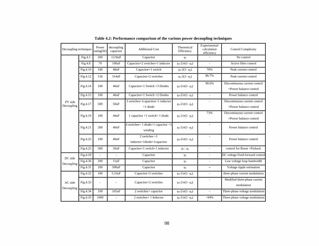
98
Table 4.2: Performance comparison of the various power decoupling techniques
Decoupling techniques Power
rating(W) decoupling capacitor
Additional Cost Theoretical Efficiency
Experimental/
calculation
efficiency
Control Complexity
PV side
Decoupling
Fig.4.5 200 13.9mF Capacitor η0 - No control
Fig.4.8 70 100uF Capacitor+2 switches+1 inductor η0-2/π(1- ηd) - Active filter control
Fig.4.10 100 40uF Capacitor+1 switch η0-2(1- ηd) 70% Peak current control
Fig.4.12 156 314uF Capacitor+2 switches η0-2(1- ηd) 86.7% Peak current control
Fig.4.14 100 46uF Capacitor+1 Switch +3 Diodes η0-2/π(1- ηd) 90.6% Discontinuous current control
+Power balance control
Fig.4.15 100 46uF Capacitor+1 Switch +2 Diodes η0-2/π(1- ηd) - Power balance control
Fig.4.17 500 50uF 3 switches+1capactitor+1 inductor
+1 diode η0-2/π(1- ηd)
- Discontinuous current control
+Power balance control
Fig.4.19 100 44uF 1 capacitor +1 switch+ 1 diode η0-2/π(1- ηd) 73% Discontinuous current control
+Power balance control
Fig.4.21 200 40uF 4 switches+ 1 diode+1 capacitor +1
winding η0-2/π(1- ηd)
- Power balance control
Fig.4.23 100 40uF 2 switches +1
inductor+1diode+1capacitor η0-2/π(1- ηd)
- Power balance control
Fig.4.25 500 50uF Capacitor+1 switch+1 inductor η0* ηd - control for Boost +Flyback
DC side
Decoupling
Fig.4.29 - - Capacitor η0 - DC voltage Feed-forward control
Fig.4.30 200 15uF Capacitor η0 - Low voltage loop bandwidth
Fig.4.31 100 500uF Capacitor η0 -- Voltage ripple estimation
AC side
Decoupling
Fig.4.32 100 5.53uF Capacitor+2 switches η0-2/π(1- ηd) - three-phase current modulation
Fig.4.33 - - Capacitor+2 switches η0-2/π(1- ηd) - Modified three-phase current
modulation
Fig.4.34 100 165uF 2 switches+ capacitor η0-2/π(1- ηd) - Three-phase voltage modulation
Fig.4.35 1000 - 2 switches+ 1 Inductor η0-2/π(1- ηd) ~94% Three-phase voltage modulation

99
4.4 Discussion
In single-stage microinverter designs, power decoupling circuits can reduce the size of
the required energy storage capacitor, thus improving the inverter lifetime, which is a
desired feature for PV-MII system. However, the power decoupling circuit will result in
additional power losses, due to the power flow through the decoupling circuit,
consequently, reducing the overall efficiency. Although the power decoupling circuit may
increase the total system’s cost due to the additional circuitry required, the extended
lifetime eliminates the reoccurring cost of inverter replacement that haunts current PV
system return on investment (ROI). To reduce the decoupling circuit power loss, the power
processed by the decoupling circuit should be minimal and limited to dcP
2 .Furthermore,
to reduce the cost of decoupling circuit and achieve high conversion efficiency, the three-
port converter with features of low component count, high integration and high conversion
efficiency is believed to be one of the best choices, with one port implementing MPPT
and a second port is dedicated for power decoupling. Recently many three-port converters
have been proposed to interface a renewable system. Two examples use a third port to
realize the power decoupling are shown in Figure 4.37 and 4.39 [104, 105].
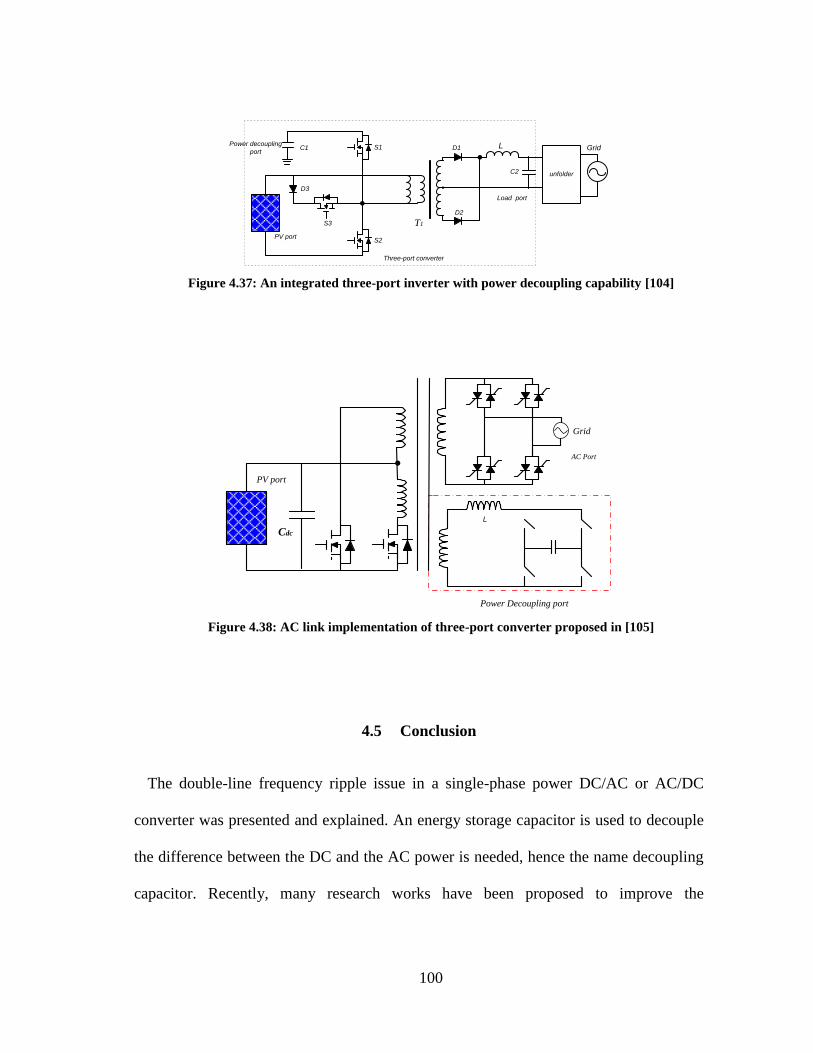
100
Figure 4.37: An integrated three-port inverter with power decoupling capability [104]
Figure 4.38: AC link implementation of three-port converter proposed in [105]
4.5 Conclusion
The double-line frequency ripple issue in a single-phase power DC/AC or AC/DC
converter was presented and explained. An energy storage capacitor is used to decouple
the difference between the DC and the AC power is needed, hence the name decoupling
capacitor. Recently, many research works have been proposed to improve the
LD1
D2
S1
S2
S3
D3
C1
C2 unfolder
Three-port converter
T1
Power decoupling
port
PV port
Load port
Grid
PV port
Cdc
AC Port
Power Decoupling port
Grid
L
101
microinverter’s reliability by using high-reliability decoupling capacitor technology. This
section reviews various power decoupling techniques that have been employed in a single-
phase microinverter to reduce the size of decoupling capacitor and improve the converter’s
lifetime expectancy. Conventionally, for single-stage inverters, the decoupling capacitor
is placed across PV module’s terminals resulting in a large size capacitor. PV-side power
decoupling circuits can be employed to reduce the capacitor size. However, the overall
inverter’s efficiency is negatively affected. Three-port converters may offer better
alternatives for single-stage inverters due to their lower cost and higher efficiency. For
multistage microinverter topologies with DC link, the DC-link capacitor offers the best
alternative for power decoupling. However, sophisticated control strategies should be
employed to allow for higher voltage ripple and to maintain a low THD in the injected
current into the grid, which will result in reducing the size of the decoupling capacitor.
Finally, AC-side decoupling involves incorporating a third phase to implement the power
decoupling, where a very small capacitance is required, but the control complexity is
increased dramatically.
102
5 DC-LINK BASED RIPPLE-PORT *
In section four, different decoupling techniques are presented that aim to cancel the
double-line frequency ripple on the DC side. However, most of the proposed techniques
depend on modifying an existed topology, and hence, each technique is tailored for a
specific topology, which makes it very difficult, if not impossible, to employ it for another
topology or power flow. This section presents a general technique that can be used to
suppress the double-line frequency ripple. Without loss of generality, the proposed
converter topology is based on the commonly used two-stage converter with a third port
is added for ripple cancellation purposes. One appreciates, however, that any topology can
be used as long as a suitable DC-link exists. Figure 5.1 shows the general block diagram
of the proposed ripple-port concept that can be applied for both DC/AC and AC/DC
single-phase power conversion. For the purpose of this dissertation, the storage element
of the ripple-port is sized for the double-line frequency component. However, in general,
the ripple-port concept can be extended to other applications.
* © 2012 IEEE. Reprinted, with permission, from S. Harb, M. Mirjafari, and R.S. Balog, “Ripple-port
Module-Integrated-Inverter for Grid-connected PV Applications,” IEEE Energy Conversion Congress and
Exposition (ECCE), September, 2012. © 2013 IEEE. Reprinted, with permission, from S. Harb, M.
Mirjafari, and R.S. Balog, “Ripple-port Module-Integrated-Inverter for Grid-connected PV Applications,”
IEEE Transactions on Industrial Applications, November, 2013. © 2013 IEEE. Reprinted, with permission,
from S. Harb and R.S. Balog, “Single-phase PWM Rectifier with Power Decoupling Ripple-port for Double-
line-frequency Ripple Cancellation,” 28th Annual IEEE Applied Power Electronics Conference and
Exposition (APEC), March, 2013.

103
Figure 5.1: A general system block diagram of the ripple-port
In the DC/AC inverter applications, a DC power source, for example a PV panel, is used
to supply power to a passive AC load or the AC grid. On the other hand, for the AC/DC
rectifier applications, an AC power source is used to supply a DC load, for example a
battery or an LED lighting system. Later in this section, analytical, simulation, and
experimental results are presented to verify the concept of the proposed ripple-port
concept for both PV energy and LED lighting applications.
Although the ripple-port concept is mainly applied for cancelling the double-line
frequency ripple that is inherent in the single-phase power converter, in general, the AC
port could be a three-phase. In a balanced three-phase system we would not expect a
double-line or a triple-line frequency ripple. However, if the system is not completely
balanced, these components could exist and the ripple-port could be used to filter them
out.
DC
Device
DC/DC
Converter
DC/AC
Converter
DC/AC
Converter
AC side
Filter
Ripple-port
FilterStorage
AC
Device Filter
DC Port AC Port
Ripple-Port
DC-Link
AC/DC Rectifier
DC/AC Inverter
Power flow
Power flow
104
This section is organized as follows, different implementation options of the ripple-port
for DC-link PV module-integrated-inverter (PV-MII) are presented in section 5.1. Also,
in section 5.1, the power process in the proposed ripple-port is explained; simulation and
experimental results are presented as well. In section 5.2, the ripple-port concept is applied
for a single-phase AC/DC rectifier application. Similarly, simulation and experimental
results are presented as well, Followed by a conclusion in section 5.3.
5.1 DC-Link-Based PV Module-Integrated-Inverter (MII)
The proposed topology, suitable for use as a module-integrated inverter (MII), is based
on the commonly used two-stage inverter with a third port is added, on the DC-link, for
ripple cancellation purposes. Later in this section, it will be shown that the double-line
frequency ripple can be filtered using a very small decoupling capacitance (CD), and, as a
result, high reliability film capacitor can be used instead of the bulky, low-reliability
electrolytic ones [25, 28, 106]. Figure 5.2 shows the system block diagram of the ripple-
port module-integrated inverter (RP-MII) in which double-frequency ripple cancellation
is accomplished by adding a “ripple-port” on the DC-link of the multi-stage inverter.
Comparing Figure 5.2 to the block diagram in Figure 5.1, the AC port consists of the
DC/AC converter, LfCf low pass filter, and the grid as load. The DC port consists of the
PV module as a power source and the DC/DC converter and filter. And finally, the ripple-
port consists of a DC/AC converter, LD low-pass filter, and the decoupling capacitor as a
load. It will be presented in section 5.2 that the same ripple-port, shown in Figure 5.2, can
be used for the AC/DC rectifier application.

105
Figure 5.2: System block diagram of the ripple-port module-integrated inverter (RP-MII)
Another advantage is that this ripple port concept can be used with any isolated DC/DC
converter topology capable of boosting the input voltage and providing galvanic isolation
for grid-connected applications. In case that galvanic isolation is not required, boost
converter can be used. However, since it has to operate at high duty ration in order to
provide a DC voltage that is compatible with the grid voltage, its efficiency will be
significantly deteriorated. Hence, a high-frequency transformer, with a suitable turn ratio,
based topology is used instead.
Consider the ripple-port that consists of an H-bridge and decoupling capacitor (CD), as
shown in Figure 5.3. Kirchoff's Voltage Law (KVL) necessitated to have an inductor (LD)
added, as a filter block, between the two different voltage source. This is to prevent the
sudden change in the decoupling capacitor’s voltage due to the H-Bridge switching effect.
GridCf
Lf
CD
LD
PV Module
PpvpAC
Pripple
Ripple Port
iLD(t)
iCD(t)
vL(t)+ +vCD(t)
-
-
V’o
(t)
Vo(t)+
-
AC Port
DC-linkCdc
DC/AC
Converter
DC/AC
Converter
DC Port
Inp
ut
Inp
ut
Ou
tpu
t
Ou
tpu
t
Inp
ut
Inp
ut
Ou
tpu
t
Ou
tpu
t
V’C
D(t
)
+
-
Ou
tpu
t
Inp
ut
DC/DC
Isolated
Converter
and filter

106
Decoupling the energy storage from the DC-link allows creation of any arbitrary voltages
across the storage device. As a result, when the circuit takes advantage of a zero-to-peak
sinusoidal energy cycle, only a very small capacitance is needed to store and deliver the
double-line frequency pulsing power in the ac system.
Figure 5.3: Ripple-port schematic
5.1.1 RP-MII implementation
The input DC/DC stage can be implemented using any DC/DC converter topology that
is capable of boosting the voltage from the PV module and providing the needed galvanic
isolation for safety purposes. In addition to the required galvanic isolation, the
transformer’s boosting capability improves the system’s efficiency. To demonstrate the
concept, the popular flyback converter is used in this section [8, 37, 39, 40, 44]. The
proposed MII can be implemented in two ways: integrated and separated ripple-port
CD
LD
Q1 Q2
Q3 Q4
Pripple
Vdc
+
-
+
-
vCD(t)iCD(t)
DC/AC Converter
Ripple-port
Filter
Ripple-port
Load
pCD
vL(t)+ -
Inp
ut
Inp
ut
Ou
tpu
t
Ou
tpu
t
107
winding. Both implementations are explored in this section along with simulation results.
However, the reliability analysis, which will be presented later in this section, shows that
the separated ripple-port winding does not add a significant improvement to the system’s
reliability. Although the separated ripple-port winding can be implemented in a way that
reduces the required decoupling capacitance, its impact on the reliability, compared to the
integrated option, is very small. The detailed analysis is presented later in this section.
Hence, only the integrated RP-MII is experimentally tested.
5.1.1.1 Integrated ripple-port (Single flyback output)
Figure 5.4 shows the implementation of the proposed RP-MII with single output flyback
converter. The ripple-port is integrated with the output port on the secondary winding of
the flyback coupled inductor. Hence, the peak voltage of the decoupling capacitor (VCD)
is constrained by the dc link. For a 235W inverter with a 200Vdc DC-link and depth of
modulation (DoM) of 0.95 for the ripple-port DC/AC inverter, a 36µF is needed according
to the equation (5.8), which is derived in section 5.1.2. However, due to imperfect coupling
between the transformer’s winding and power losses through the system, a slightly larger
decoupling capacitance is needed in practice, since the calculation is based on the ideal
lossless system.
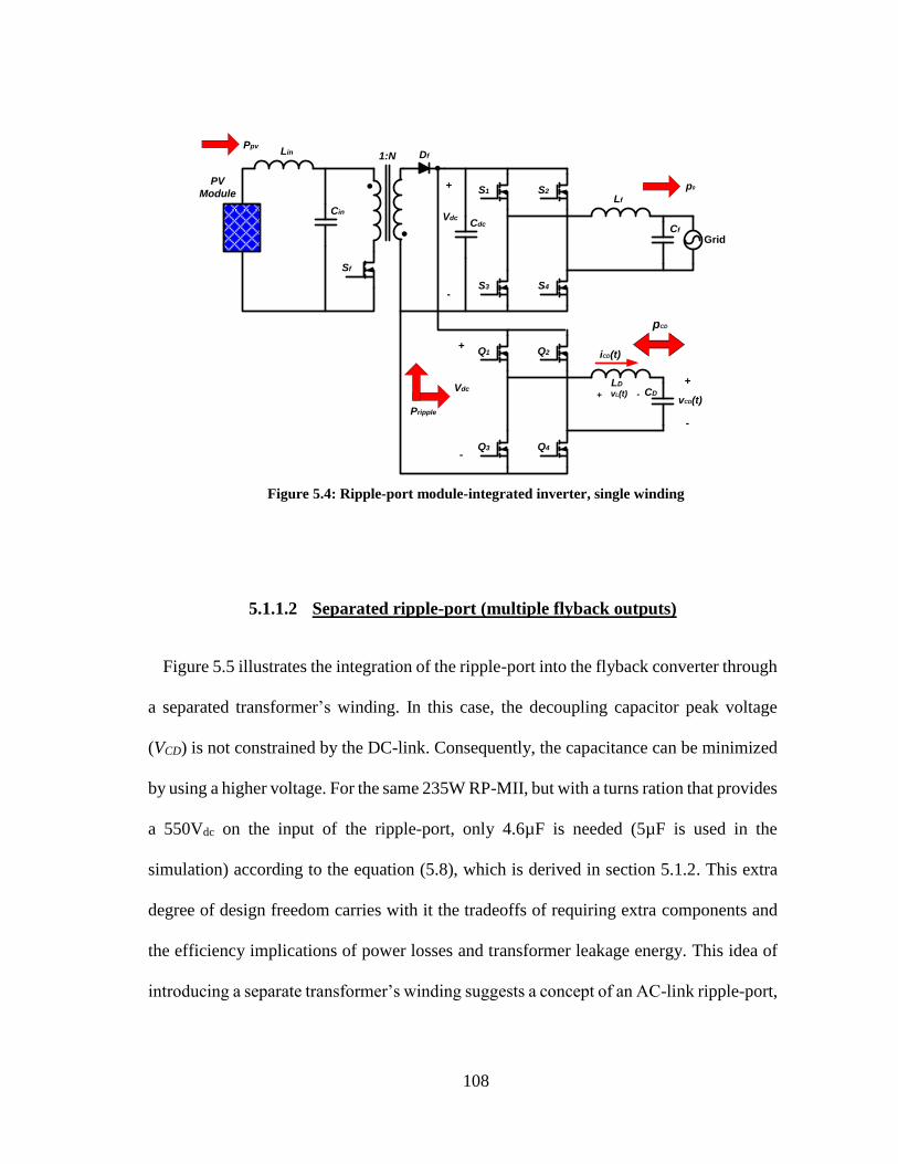
108
Figure 5.4: Ripple-port module-integrated inverter, single winding
5.1.1.2 Separated ripple-port (multiple flyback outputs)
Figure 5.5 illustrates the integration of the ripple-port into the flyback converter through
a separated transformer’s winding. In this case, the decoupling capacitor peak voltage
(VCD) is not constrained by the DC-link. Consequently, the capacitance can be minimized
by using a higher voltage. For the same 235W RP-MII, but with a turns ration that provides
a 550Vdc on the input of the ripple-port, only 4.6µF is needed (5µF is used in the
simulation) according to the equation (5.8), which is derived in section 5.1.2. This extra
degree of design freedom carries with it the tradeoffs of requiring extra components and
the efficiency implications of power losses and transformer leakage energy. This idea of
introducing a separate transformer’s winding suggests a concept of an AC-link ripple-port,
GridCf
Lf
CD
LD
Cdc
Df
Cin
Lin
PV
Module
Sf
S1 S2
S3 S4
Q1 Q2
Q3 Q4
Ppv
p0
Pripple
1:N
Vdc
Vdc+
-
vCD(t)
iCD(t)
pCD
+
-
+
-
vL(t)+ -

109
which will be fully explored in section seven. Table 5. 1 compares the two implementation
approaches.
Figure 5.5: Ripple-port module-integrated inverter, multiple windings
Table 5.1: A comparison of ripple-port implementations
Implementation
approach
Decoupling
capacitance (CD)
DC-link
voltage
Complexity
Integrated winding 36µF 200 V No additional components
Separated winding 4.6 µF 550 V Extra transformer winding, DC-link
capacitor, and bidirectional switch on
the DC input side of the ripple-port
GridCf
Lf
CD
LD
Cdc_1
Df_1
Cin
Lin
PV
Module Sf
S1 S2
S3 S4
Q1 Q2
Q3 Q4
Ppv
p0
Pripple
1:N2:N3
Cdc_2
Sf_2
Vdc
Vrip
pCD
+
-
vCD(t)
iCD(t)
vL(t)+ -
110
5.1.2 Ripple-port power processing
Figure 5.2 illustrates the voltage polarity and current direction in the ripple-port
load/source (LD and CD). A small inductor is used to satisfy KVL and prevent sudden
changes in the capacitor’s voltage because of the switching effect. Assuming unity power
factor, the output power given in (4.5) becomes as given in (5.1), which has a constant
average value and a double-line frequency component.
toPVP
PVPtp 2cos)(
0 (5.1)
where g
Ig
VPVP2
1
Since, the ripple-port is processing the power on the DC-link, this implies that the phase
shit effect of the AC port low pass filter should be taken into consideration in order to
achieve an accurate ripple cancellation on the DC side. This can be accomplished by
considering the power on the input of the AC output port filter. Considering a LC low pass
filter in Figure 5.6 with a transfer function of G, the voltage ( )('0 tv ) on the input side of
the AC port filter is given in (5.2), where only the fundamental component is considered.

111
Figure 5.6: Low pass filter block diagrm
G
tvtv
)(0)('
0 , (5.2)
where
filtertoVtv sin
'0)(
'0 ,
G
tv
filter
)(0 is the phase shift introduced by the filter,
G is the input-to-output voltage transfer function.
For the specific filter configuration shown in Figure 5.6, )(
'0 tv
is given in (5.3).
)(0)('0 tv
fCZ
fLZ
fCZ
tv
, (5.3)
Where ZCf and ZLf are the capacitor and inductor impedances, respectively.
V’0(t) v0(t)
+
-
+
-
Low pass filter
Transfer function (G)
Cf
Lf
Inp
ut
Ou
tpu
t
112
An ideal output LC filter will not alter the phase of the output voltage. However, in
practice, both the inductor and the capacitor have series resistance, and thus, the amplitude
and the phase of the output voltage will be affected by the LfCf filter. The impact of the
LC filter on the amplitude is insignificant, and can be neglected. Consequently, the power
that is processed by the AC port H-bridge should take the phase shift introduced by the
filter as given in (5.4)
filter
toPVP
PVPtp 2cos)(
0 (5.4)
On the other hand, the input power, extracted from the PV module, is controlled at a
constant value, PVP , based upon the available maximum power point. Then, the ripple-port
will be processing the difference between the input and the output power as given in (5.5)
)(0
)( tpPV
Ptripp (5.5)
The power processed by the ripple-port is the total power processed by the decoupling
capacitor, CD, and the inductor, LD, which is calculated as follows:
113
)()()()()()()( tD
Cit
DC
vtD
Lit
DL
vtD
Cpt
DL
ptripp (5.6)
However, the same current flows in both LD and CD, which it is given in (5.7), assuming
vCD(t)=sin(ω0t+ϕ). Then, )(tprip as function of LD, CD, and the peak capacitor voltage is
given in (5.8).
tooDC
DC
Vdt
tD
Cdv
DCt
DCi cos
)(
)(
(5.7)
t
oD
CVt
ooDC
DC
VtD
Cvt
DCitripp sincos)(*)()(
toD
CD
LooDC
DC
V
tripp 2sin2
212
)(
(5.8)
Substituting (5.4) and (5.8) in (5.5), the required decoupling capacitance, CD, and the
phase angle (ϕ) of the voltage across the decoupling capacitor is calculated as shown in
(5.9) and (5.10) [36]

114
D
CD
LooD
CV
PVP
DC
212
2
,
(5.9)
and
tfilter
t0
2sin0
2cos
filter
4
(5.10)
The AC port’s LC filter and the ripple-port’s L filter introduce a small phase shift, as
shown in Figure 5.6. This phase shit needs to be taken in consideration in the control
design.
From (5.9), it is clear that a tradeoff exists between the value of the decoupling
capacitance (CD) and the peak capacitor voltage (VCD). The latter will determine the
stresses on the power switches, which, in turn, affects the efficiency and the cost of the
inverter. Controlling voltage across the decoupling capacitor (vCD(t)) according to (5.9)
and (5.10) will result in a balance three-port system. Figure 5.6 shows the output voltage
and the voltage across the decoupling capacitor with a clear 45 degree phase shift. Figure
5.7 shows power waveforms of the RP-MII, where the double-line frequency ripple, on
the input side, is eliminated.
The aforementioned analysis shows that the key of the ripple cancellation process, using
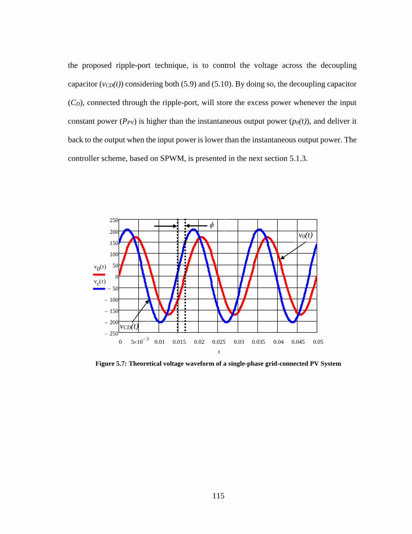
115
the proposed ripple-port technique, is to control the voltage across the decoupling
capacitor (vCD(t)) considering both (5.9) and (5.10). By doing so, the decoupling capacitor
(CD), connected through the ripple-port, will store the excess power whenever the input
constant power (PPV) is higher than the instantaneous output power (p0(t)), and deliver it
back to the output when the input power is lower than the instantaneous output power. The
controller scheme, based on SPWM, is presented in the next section 5.1.3.
Figure 5.7: Theoretical voltage waveform of a single-phase grid-connected PV System
0 5 103
0.01 0.015 0.02 0.025 0.03 0.035 0.04 0.045 0.05
250
200
150
100
50
0
50
100
150
200
250
v0 t( )
vc t( )
t
ϕ
vCD(t)
v0(t)

116
Figure 5.8: Theoretical power waveform of a single-phase grid-connected PV System
From (5.9), it is clear the relationship between the power level, decoupling capacitor’s
voltage (VCD), and the decoupling capacitance. Since the latter is a design parameter that
cannot be changed during the operation. Hence, the only parameter that can and needs to
be modified in order to cancel the double-line frequency is VCD. This can be accomplished
by modifying the DoMRP of the ripple-port DC/AC converter. Assuming CD and LD are
very small, VCD is calculated as given in (5.11) for different operating power, and then,
the DoMRP is calculated by (5.12). This value will be fed to the SPWM modulator.
DCo
PVP
VCD
2 (5.11)
0 0.01 0.02 0.03 0.04 0.05400
200
0
200
400
600
p0 t( )
pripple t( )
Ppv
t
pCD(t)
p0(t) PPV
p0(t)
pCD(t)
PPV

117
dc
CDRP
V
VDoM (5.12)
For 235W and 200Vdc PV-MII system, figure 5.9 shows how the DoMRP changes as the
operating power changes. Also, it shows the relationship between the DoMRP and the
operating power at different decoupling capacitor (CD) design values. Figure 5.9 shows
the CD’s values that guarantee the double-line frequency ripple cancellation without an
overmodulation operation mode. It shows that as the CD increases the DoMRP range
decreases for the expected operating power levels. This indicates a tradeoff problem
between using smaller CD, which results in a lower cost, and the narrow DoMRP, which
results in optimum conversion efficiency. However, there are many factors that play a role
in the design process. For example, using smaller CD means high peak voltage across its
terminals (according to (5.9)). The higher DC-link voltage can be achieved using higher
number of transformer’s turns. Having a high DC-link voltage has two negative impacts,
higher voltage stress on semiconductor devices and higher conduction power loss in the
transformer’s turns. In [107-109], a multi-objective optimization methodology is
presented and applied for different power electronic applications. It takes into account the
usage model of the application in order to find the optimum design. A new high-frequency
magnetic modeling technique, for power electronics converters, is presented in [110-112],
where the finite element analysis is used to determine the parasitic components of high-
frequency magnetics’ windings and its impact on the overall system’s performance.
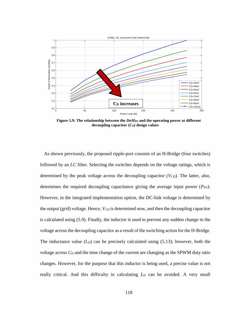
118
Figure 5.9: The relationship between the DoMRP and the operating power at different
decoupling capacitor (CD) design values
As shown previously, the proposed ripple-port consists of an H-Bridge (four switches)
followed by an LC filter. Selecting the switches depends on the voltage ratings, which is
determined by the peak voltage across the decoupling capacitor (VCD). The latter, also,
determines the required decoupling capacitance giving the average input power (PPV).
However, in the integrated implementation option, the DC-link voltage is determined by
the output (grid) voltage. Hence, VCD is determined now, and then the decoupling capacitor
is calculated using (5.9). Finally, the inductor is used to prevent any sudden change in the
voltage across the decoupling capacitor as a result of the switching action for the H-Bridge.
The inductance value (LD) can be precisely calculated using (5.13); however, both the
voltage across CD and the time change of the current are changing as the SPWM duty ratio
changes. However, for the purpose that this inductor is being used, a precise value is not
really critical. And this difficulty in calculating LD can be avoided. A very small
0 50 100 150 200 2500.1
0.2
0.3
0.4
0.5
0.6
0.7
0.8
0.9
1DoMrp, CD, and power level relationship
Power Level (W)
De
pth
of M
od
ula
tio
n (
Do
Mrp
)
CD=30uF
CD=40uF
CD=50uF
CD=60uF
CD=70uF
CD=80uF
CD=90uF
CD=100uFCD increases
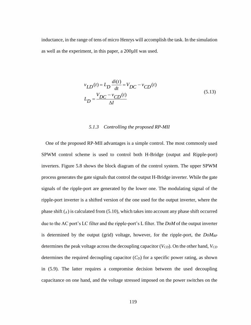
119
inductance, in the range of tens of micro Henrys will accomplish the task. In the simulation
as well as the experiment, in this paper, a 200µH was used.
I
tCD
vDC
V
DL
tCD
vDC
Vdt
tdiD
LtLD
v
)(
)()(
)(
(5.13)
5.1.3 Controlling the proposed RP-MII
One of the proposed RP-MII advantages is a simple control. The most commonly used
SPWM control scheme is used to control both H-Bridge (output and Ripple-port)
inverters. Figure 5.8 shows the block diagram of the control system. The upper SPWM
process generates the gate signals that control the output H-Bridge inverter. While the gate
signals of the ripple-port are generated by the lower one. The modulating signal of the
ripple-port inverter is a shifted version of the one used for the output inverter, where the
phase shift ( ) is calculated from (5.10), which takes into account any phase shift occurred
due to the AC port’s LC filter and the ripple-port’s L filter. The DoM of the output inverter
is determined by the output (grid) voltage, however, for the ripple-port, the DoMRP
determines the peak voltage across the decoupling capacitor (VCD). On the other hand, VCD
determines the required decoupling capacitor (CD) for a specific power rating, as shown
in (5.9). The latter requires a compromise decision between the used decoupling
capacitance on one hand, and the voltage stressed imposed on the power switches on the
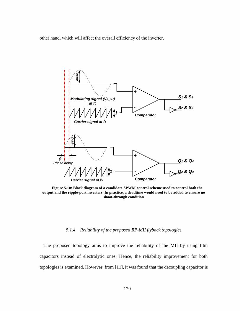
120
other hand, which will affect the overall efficiency of the inverter.
Figure 5.10: Block diagram of a candidate SPWM control scheme used to control both the
output and the ripple-port inverters. In practice, a deadtime would need to be added to ensure no
shoot-through condition
5.1.4 Reliability of the proposed RP-MII flyback topologies
The proposed topology aims to improve the reliability of the MII by using film
capacitors instead of electrolytic ones. Hence, the reliability improvement for both
topologies is examined. However, from [11], it was found that the decoupling capacitor is
Carrier signal at fs
Modulating signal (V0_ref)
at f0
Phase delay
Carrier signal at fs
+
+
-
-
S1 & S4
S2 & S3
Q1 & Q4
Q2 & Q3
Comparator
Do
M0
Do
Mr
1
1
Comparator

121
the limiting component whether electrolytic or film is used. The failure rate of the film
capacitor is found using (5.14) [31]:
EQCVbP (5.14)
λb is given in (5.15), which is function of the operating temperature (T (C)) and voltage
stress (S). These two factors are operating factors.
18
398
2735.2exp1
5
4.000099.0
TS
b (5.15)
Thus, λb, πQ, and πE all operating-related factors, and will be the same for both
configurations (integrated and separated options). Hence, they can be factored out, and λP
is function of just the capacitance factor, πCV, which is for film capacitor is calculated by
(5.16)
085.01.1 CCV
(5.16)
Then, the failure rate of the decoupling capacitor is given (5.17)

122
CVP
(5.17)
where EQb
Evaluating the failure rate for both configurations, with 36µF used in the first
configuration in Figure 5.4, and two 5µF capacitors in the second configuration in Figure
5.5, the capacitance factors are calculated in (5.18).
492.11
492.1085.0
361.11 PCV
522.2261.122
261.1085.0
51.12 PCV
(5.18)
Then, the conclusion is that the number of capacitors used has a stronger effect on the
failure rate than the value of the capacitance itself. Moreover, the lifetime projection
formula in (5.19) [46] does not depend on the capacitance value, consequently, both
decoupling will have the same expected lifetime, providing the same operating conditions
123
5167.06087.2
1020
rVopV
rV
opV
Tref
T
L
L (5.19)
where L0 is the basic (test) lifetime, Vop is the operating voltage, Vref is the rated voltage,
T is the operating temperature, and Tref is the test temperature.
As a result, from reliability point view, using film capacitor, regardless of its value, will
improve the overall reliability of the inverter for the specific PV-MII studied in this
section.
5.1.5 Simulation results for the DC-link MII
Consider the 235W system, the component values of the RP-MII topology, shown in
Figure 5.4, are listed in Table 5.2. PSIM was used to verify the validity of the proposed
RP-MII shown in Figure 5.4. Figure 5.11 shows the schematic of the system. The flyback’s
transformer is assumed to have a perfect coupling. DC-link, output, and decoupling
capacitor voltages are shown in Figure 5.12. Figure 5.13 shows that the input, output, and
ripple power waveforms match the theoretical waveforms in Figure 5.7. Figure 5.14
reveals that processing 238W results in less than a 1W ripple (0.42% power ripple) on the
input. It shows a 51 degree phase shift between v0(t) and vCD(t). Figure 5.15 shows the
FFT waveform of the input power.
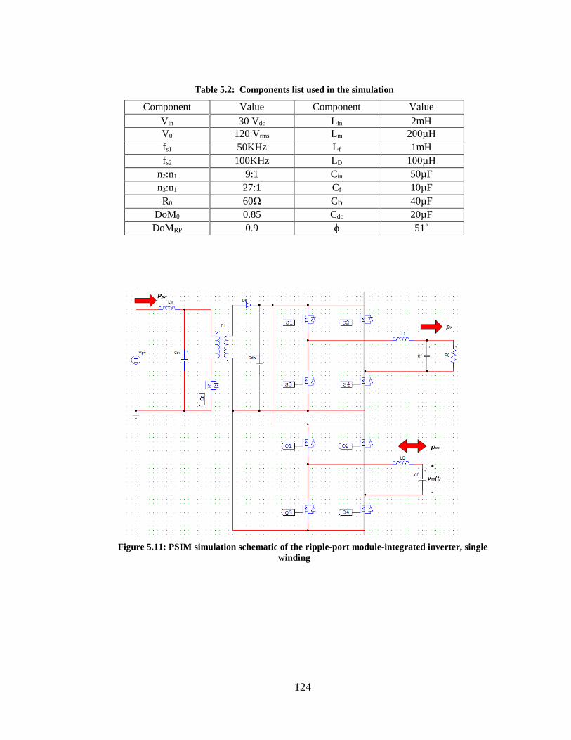
124
Table 5.2: Components list used in the simulation
Component Value Component Value
Vin 30 Vdc Lin 2mH
V0 120 Vrms Lm 200µH
fs1 50KHz Lf 1mH
fs2 100KHz LD 100µH
n2:n1 9:1 Cin 50µF
n3:n1 27:1 Cf 10µF
R0 60Ω CD 40µF
DoM0 0.85 Cdc 20µF
DoMRP 0.9 ϕ 51˚
Figure 5.11: PSIM simulation schematic of the ripple-port module-integrated inverter, single
winding
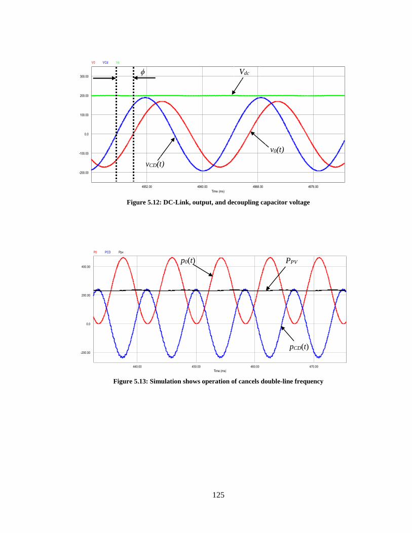
125
Figure 5.12: DC-Link, output, and decoupling capacitor voltage
Figure 5.13: Simulation shows operation of cancels double-line frequency
4952.00 4960.00 4968.00 4976.00
Time (ms)
0.0
-100.00
-200.00
100.00
200.00
300.00
V0 VCd Vs
440.00 450.00 460.00 470.00
Time (ms)
0.0
-200.00
200.00
400.00
P0 PCD Ppv
p0(t) PPV
pCD(t)
ϕ
vCD(t)
v0(t)
Vdc
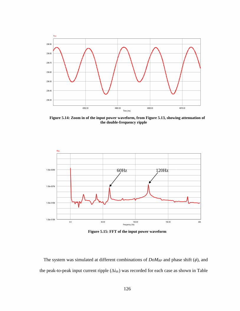
126
Figure 5.14: Zoom in of the input power waveform, from Figure 5.13, showing attenuation of
the double-frequency ripple
Figure 5.15: FFT of the input power waveform
The system was simulated at different combinations of DoMRP and phase shift (ϕ), and
the peak-to-peak input current ripple (Δidc) was recorded for each case as shown in Table
4952.00 4960.00 4968.00 4976.00
Time (ms)
238.30
238.40
238.50
238.60
238.70
238.80
238.90
Ppv
0.0 50.00 100.00 150.00 200.00
Frequency (Hz)
1.00e-013M
1.00e-010M
1.00e-007M
1.00e-004M
Ppv
60Hz 120Hz

127
5.3. These results are shown in Figure 5. 16, which shows a unique operation point
(DoMRP,ϕ) that results in the minimum double-line frequency ripple.
Table 5.3: Simulation results at different DoMRP and phase shift (ϕ) combinations
ϕ 46 degree 48 degree 50 degree 52 degree 54 degree
DoMRP Δidc (A) % Δidc
(A)
% Δidc (A) % Δidc
(A)
% Δidc
(A)
%
0.87 1.68 21.54 1.32 16.92 1.1 14.1 1.19 15.26 1.45 18.59
0.90 1.42 18.2 0.9 11.54 0.62 7.95 0.73 9.36 1.17 15
0.93 1.28 16.4 0.77 9.87 0.22 2.82 0.49 6.28 0.96 12.3
0.96 1.4 17.95 0.89 11.4 0.55 7.05 0.69 8.85 1.12 14.36
0.99 1.7 21.8 1.45 18.6 1.19 15.26 1.28 16.4 1.58 20.26

128
Figure 5.16: Double-line frequency ripple as a function of DoMRP and phase shift (ϕ)
5.1.6 Experimental results
The ripple-port concept was experimentally tested using the new Solar_HV_DC_AC kit
from Texas Instruments (TMDSHV1PHINVKIT) [113]. It is an IGBTs-based full bridge
inverter followed by a low pass filter (LC-filter). Two identical boards were used to
implement the AC port and the ripple-port DC/AC converters shown in Figure 5.2. Figure
5.17 show the experiment setup of the RP-MII. Table 5.4 lists the values of the
components used in the experiment test. Both boards were controlled by the PWM signals
generated using a single TI Delfino microcontroller (TMS320F28335). Figure 5.18 shows
the output (v0(t)) and decoupling capacitor (vCD(t)) voltages and the resulting AC

129
component of the input current. The depth of modulation (DoM) for the output H-Bridge
was kept constant at 0.85. The depth of modulation of the ripple-port H-Bridge (DoMRP)
and the phase angle (ϕ) were manually tuned to minimize the double-line frequency ripple
on the input side. The waveform in Figure 5.18 shows that the input current ripple is
suppressed to less than 10% peak-to-peak, and this at DoMRP = 0.848 and ϕ = 51.5°, which
results in a peak vCD(t) voltage of 102V. Figure 5.19 shows the input current along with
its experimentally measured FFT, which confirms that the 120Hz frequency has been
suppressed to the same amplitude as the other low-order harmonics (-46.4dB).
Table 5.4: DC/AC inverter experimental components values
Component Value Component Value
Vin 120Vdc Iin 500mA
Lf 3.5mH Cf 1µF
R0 70Ω LD 100µH
CD 40µF Cin 40 µF

130
Figure 5.17: Ripple-port experiment set up
Figure 5.18: Experimental waveform - AC port output voltage, ripple-port decoupling capacitor
voltage, and the DC port input current ripple
Input Voltage
AC output side
H-Bridge
Ripple-port
H-Bridge
Resistive
Load
Ripple-port
LD & CD
Microcontroller
Board
φ
Decoupling capacitor voltage
AC output voltage
Input Current ripple

131
Figure 5.19: Input current (top trace), and the FFT experimental measurement (bottom trace)
To examine the efficacy of the ripple-port, the DoMRP was reduced to 0.5, while the
value of ϕ is kept the same as in the previous case. The results, shown in Figure 5.20,
clearly show the double-line frequency ripple on the input side. In this case, the input
current ripple is 476m peak-to-peak. Figure 5.21 shows the input current and its
experimentally measured FFT, which is 30dB higher than what was achieved with manual
tuning in Figure 5.19.
120 HZ
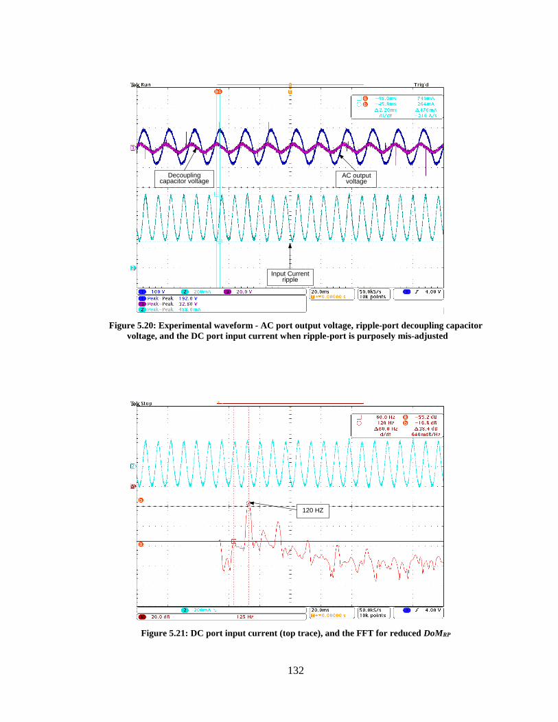
132
Figure 5.20: Experimental waveform - AC port output voltage, ripple-port decoupling capacitor
voltage, and the DC port input current when ripple-port is purposely mis-adjusted
Figure 5.21: DC port input current (top trace), and the FFT for reduced DoMRP
Decoupling capacitor voltage
AC output voltage
Input Current ripple
120 HZ

133
Table 5.5: Comparison of the operation with different DoMRP
DC port input current
ripple (Δidc)
120 Hz of the DC port
input current
120 Hz
relating to DC
Ripple-port activated 48m A -46.4 dB 40 dB
Ripple-port deactivated 476m A -16.8 dB -38 dB
Ripple-port suppression 29.6 dB
5.2 Single-phase rectifier with ripple-port
In this section, the ripple-port concept is applied to a single-phase PWM rectifier that
eliminates the need for the electrolytic capacitor. Consequently, this improves the
reliability of the system that is suitable for long-life applications such as LED lighting. A
generic block diagram of an AC/DC rectifier system with the ripple-port is shown in
Figure 5.22, which is derived from the block diagram in Figure 5.1. This evidently show
the modularity feature of the proposed ripple-port techniques unlike other decoupling
techniques presented in section four.
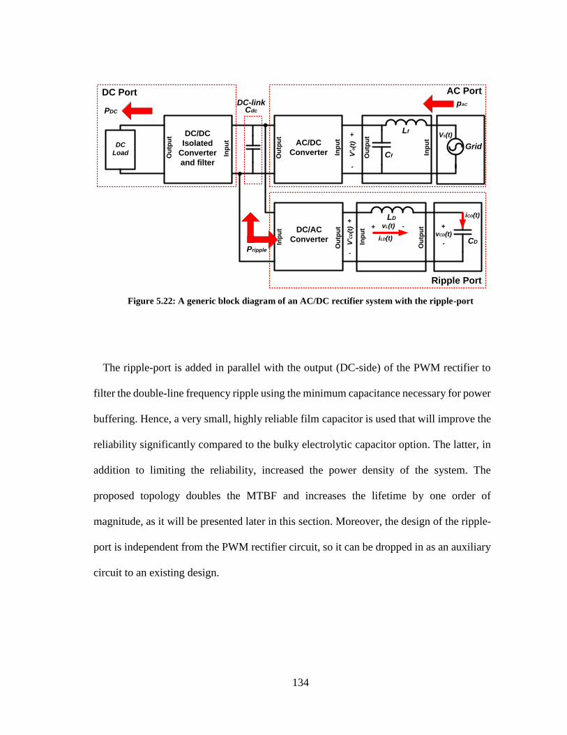
134
Figure 5.22: A generic block diagram of an AC/DC rectifier system with the ripple-port
The ripple-port is added in parallel with the output (DC-side) of the PWM rectifier to
filter the double-line frequency ripple using the minimum capacitance necessary for power
buffering. Hence, a very small, highly reliable film capacitor is used that will improve the
reliability significantly compared to the bulky electrolytic capacitor option. The latter, in
addition to limiting the reliability, increased the power density of the system. The
proposed topology doubles the MTBF and increases the lifetime by one order of
magnitude, as it will be presented later in this section. Moreover, the design of the ripple-
port is independent from the PWM rectifier circuit, so it can be dropped in as an auxiliary
circuit to an existing design.
GridCf
Lf
CD
LD
DC
Load
PDC
pAC
Pripple
Ripple Port
iLD(t)
iCD(t)
vL(t)+ +vCD(t)
-
-
V’o
(t)
Vs(t)+
-
AC Port
DC-linkCdc
AC/DC
Converter
DC/AC
Converter
DC Port
Ou
tpu
t
Inp
ut
DC/DC
Isolated
Converter
and filter
Ou
tpu
t
Inp
ut
Ou
tpu
t
Inp
ut
V’C
D(t
)
+
-
Ou
tpu
t
Inp
ut
Ou
tpu
t
Inp
ut
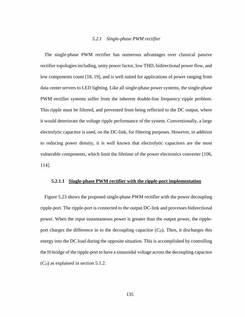
135
5.2.1 Single-phase PWM rectifier
The single-phase PWM rectifier has numerous advantages over classical passive
rectifier topologies including, unity power factor, low THD, bidirectional power flow, and
low components count [18, 19], and is well suited for applications of power ranging from
data center servers to LED lighting. Like all single-phase power systems, the single-phase
PWM rectifier systems suffer from the inherent double-line frequency ripple problem.
This ripple must be filtered, and prevented from being reflected to the DC output, where
it would deteriorate the voltage ripple performance of the system. Conventionally, a large
electrolytic capacitor is used, on the DC-link, for filtering purposes. However, in addition
to reducing power density, it is well known that electrolytic capacitors are the most
vulnerable components, which limit the lifetime of the power electronics converter [106,
114].
5.2.1.1 Single-phase PWM rectifier with the ripple-port implementation
Figure 5.23 shows the proposed single-phase PWM rectifier with the power decoupling
ripple-port. The ripple-port is connected to the output DC-link and processes bidirectional
power. When the input instantaneous power is greater than the output power, the ripple-
port charges the difference in to the decoupling capacitor (CD). Then, it discharges this
energy into the DC load during the opposite situation. This is accomplished by controlling
the H-bridge of the ripple-port to have a sinusoidal voltage across the decoupling capacitor
(CD) as explained in section 5.1.2.

136
Figure 5.23: Single-phase PWM rectifier with power decoupling ripple-port
5.2.2 Double-line frequency ripple cancellation
The analysis in this subsection is very similar to the analysis in section 5.1.2. However,
in order to have a complete and comprehensive explanation for the ripple-port, it will be
presented here considering a rectifying mode. The ripple port is connected to the dc output
of the PWM rectifier, as shown in Figure 5.23. Without loss of generality, assuming unity
power factor the instantaneous AC input power ps(t) is given in (5.20), and assuming a
lossless converter, the average power from the source Ps_av and the output dc power Po are
vs
Ls
Cdc
Q1
Q3
Q2
Q4
S1
S3
S2
S4
R0
CD
LD
Vdc
Pripple
P0
PS
+
-

137
equal. Then, the double-line frequency, time varying power pdf(t) from the ac source must
appears on the DC-link (the output side). This power ripple is manifested as voltage ripple
on the output capacitor, and must be filtered by the ripple-port to improve the performance
of the rectifier. In LED applications, this double-line frequency ripple will negatively
affect the efficacy of the LED light, and thus, results in an unstable light output and the
potential to shorten the LED operating lifetime. This implies that the ripple-port has to be
capable of processing the power given (5.21).
)(_02cos
22)( t
dfpavsPtsIsVsIsV
tsp (5.20)
)()( tdf
ptripple
p
(5.21)
The amplitude (VCD), and the phase angle (ϕ) of the ripple-port capacitor voltage
required to cancel the double-line frequency ripple on the dc output port is given by (5.9)
and (5.10); where θ is the phase shift in the output voltage caused by the filter components,
including LD and input L-C low pass filter, as well as the phase shift due to non-unity
power factor. Complete analysis of the double-frequency ripple cancellation process can
be found in [36, 115].
Imposing the conditions in (5.9) and (5.10) for controlling the ripple-port, the input,
output, and the ripple-port power are balanced as shown in Figure 5.24 for a 1kW rectifier

138
system. Figure 5.24 illustrates the ripple-port storing energy by charging the decoupling
capacitor (positive pripple) when the instantaneous input power is greater than the output
power, and discharging the decoupling capacitor (negative pripple) when the input power is
less than the output power.
Figure 5.24: Input, output, and ripple power waveforms
5.2.3 Parameters design
The values of the input (Ls) and the decoupling (LD) inductors are functions of the
switching frequency and the power rating. The inductance varies inversely with the
average input power (Ps_av = P0) [18] and the design must handle the required peak current
and current ripple. For example, at 1kW, the required input inductance is 1.5mH, while
Charging
Discharging
ps(t)
pripple(t)
P0

139
for 100W, 14mH is required. Similarly, for the decoupling circuit, 500µH is needed for
1KW, and 3.4mH for 100W. With the ripple port managing the 120Hz power, the DC-link
capacitor (Cdc) is only needed to filter high frequency switching ripple. For a 1kW system,
80µF will suffice. On the ripple-port, the double-line frequency ripple is cancelled by the
decoupling capacitor (CD), which is calculated from (5.9). For a 1kW system switching at
100 kHz, only 140µF is needed.
5.2.4 Reliability of the proposed rectifier topology
The proposed single-phase PWM rectifier uses two film capacitors, 80µF across the DC-
link and 140µF as a decoupling capacitor. The reliability analysis, for both the
conventional electrolytic capacitor option (1,330µF) and the ripple-port capacitor showed
that the proposed rectifier topology has improved the MTBF by a factor of more than two,
and the lifetime by an order of magnitude, as it is shown in Figure 5.25. MIL-HDBK-217
[31] is used to calculate the MTBF for both options, and the results are shown in Table
5.5. It is worth mentioning that a temperature usage model approach can be used for
evaluating the MTBF, such as the one developed for PV inverters [115], instead of a
singular operating temperature to present a more realistic assessment of true expected
MTBF. This is particularly relevant for outdoor applications of the circuit.

140
Table 5.6: Comparison of the calculated MTBF for a conventional design with electrolytic capacitor
and the ripple-port with film capacitor
Conventional design Ripple-port
Capacitance 1,330µF 80µF+140µF
Number of MOSFETs 4 8
MTBF (million hours) 1.1758 2.3480
Figure 5.25: Lifetime projection for the conventional dc bus design with electrolytic capacitor
(LE-DC) and the proposed ripple-port with film capacitor (LF). Over the entire temperature range
the film capacitors exhibit superior longevity
5.2.5 Simulation results for the DC-link AC/DC
A 1kW single-phase PWM rectifier, which rectifies a 170Vp sinusoidal input voltage
from the utility into a regulated 200V at the output, was simulated in PSIM. In Figure
0 10 20 30 40 50 60 70 80 90 1001 10
4
1 105
1 106
1 107
1 108
1 109
Operating Temperature (°C)
Lif
etim
e (H
ours
)
LE_DC Tc
LF Tc
Tc

141
5.26, the system’s schematic is shown. Table 5.6 lists the parameters used in the
simulation. In a conventional circuit, 1,330µF is required on the DC-link. However, using
the ripple-port, only 80µF on the DC-link and 140µF for the ripple-port decoupling
capacitor are required. Figure 5.27 shows the input ps(t), output P0, and ripple-port prip(t)
power waveforms, which matches with the theoretical waveforms in Figure 5.24. Figure
5.27 also shows the double-line frequency power ripple that has been suppressed to a very
small level with only 5% peak-to-peak ripple, which was arbitrarily chosen to prove the
concept and can be further reduced in practice.
Table 5.7: AC/DC rectifier with ripple-port simulation parameters
Component Value Component Value
Vs 120 Vrms Ro 40
Is 12.5Ap fs 100KHz
Ls 1.5mH Kpv 0.01
Cdc 80uF Kiv 100
CD 140uF Kpi 5
LD 100uH Kii 500
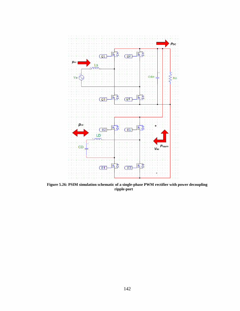
142
Figure 5.26: PSIM simulation schematic of a single-phase PWM rectifier with power decoupling
ripple-port

143
Figure 5.27: Simulation results - input, output, and ripple power waveforms
Figure 5.28 shows the output voltage, V0, and current, I0. Both show approximately 5%
peak-to-peak ripple. In Figure 5.29, it is clearly observed that the input current is(t) is in
phase with the input voltage vs(t). This is verified by nearly unity power factor as shown
in Figure 5.30. Figure 5.31 shows the calculated FFT for the input current is(t), which
indicates a very low THD. The calculated THD is 3.5%. On the DC-link side, Figure 5.32
shows the calculated FFT of the output power P0, and it is clearly noticeable how the
double-line frequency component is suppressed to a very low level (less than 5%). Figure
5.33 shows the regulated output voltage (V0) on top of the input voltage (vs(t)) and the
voltage across the decoupling capacitor (vCD(t)). It shows the 46 degree phase shift
between vs(t) and vCD(t).
385.00 390.00 395.00 400.00 405.00
Time (ms)
0.0K
-0.50K
-1.00K
0.50K
1.00K
1.50K
2.00K
P0 prip ps
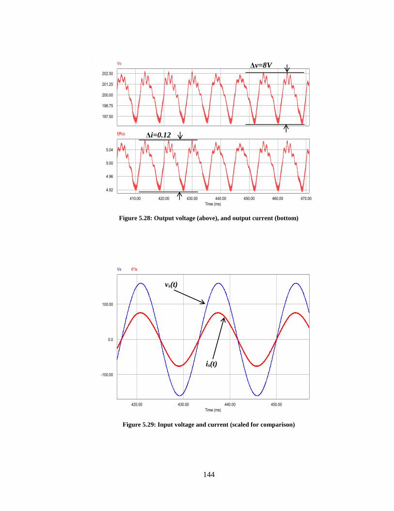
144
Figure 5.28: Output voltage (above), and output current (bottom)
Figure 5.29: Input voltage and current (scaled for comparison)
197.50
198.75
200.00
201.25
202.50
Vo
410.00 420.00 430.00 440.00 450.00 460.00 470.00
Time (ms)
4.92
4.96
5.00
5.04
I(Ro)
420.00 430.00 440.00 450.00
Time (ms)
0.0
-100.00
100.00
Vs 6*Is
Δv=8V
Δi=0.12
A
is(t)
vs(t)

145
Figure 5.30: Power factor nearly unity (0.99)
Figure 5.31: Calculated FFT of the input current (is(t))
0.0 0.10 0.20 0.30 0.40 0.50
Time (s)
0.0
-0.20
0.20
0.40
0.60
0.80
1.00
VAPF1_PF
0.0 200.00 400.00 600.00 800.00
Frequency (Hz)
0.0
2.00
4.00
6.00
8.00
10.00
12.00
Is
60Hz
180Hz
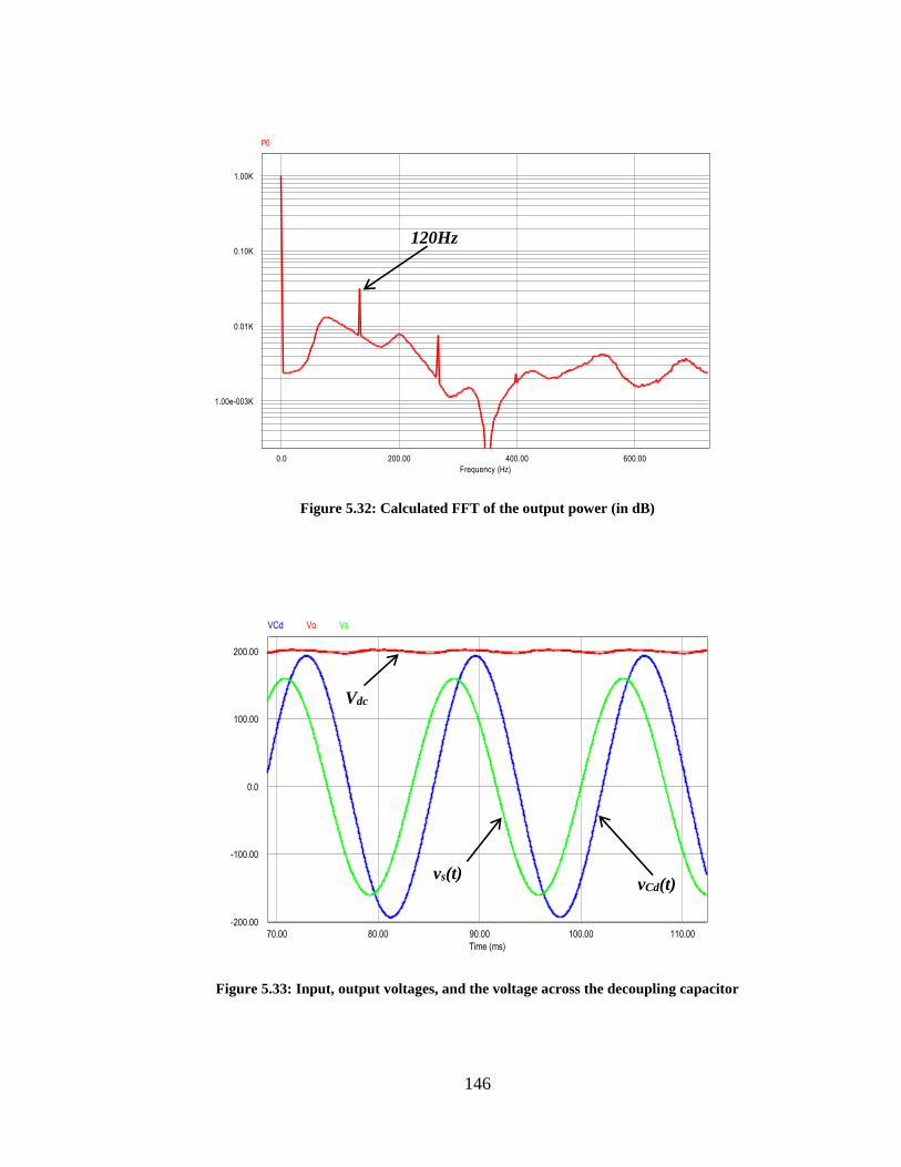
146
Figure 5.32: Calculated FFT of the output power (in dB)
Figure 5.33: Input, output voltages, and the voltage across the decoupling capacitor
0.0 200.00 400.00 600.00
Frequency (Hz)
1.00e-003K
0.01K
0.10K
1.00K
P0
70.00 80.00 90.00 100.00 110.00
Time (ms)
0.0
-100.00
-200.00
100.00
200.00
VCd Vo Vs
120Hz
vs(t) vCd(t)
Vdc

147
5.2.6 Experimental results – AC/DC rectifier with ripple-port
Figure 5.34 shows the experiment setup for the single-phase AC/DC rectifier with the
proposed ripple-port. The AC/DC rectifier stage is implemented using the evaluation
board from TI (UCC28070EVM). It consists of a diode bridge and two-phase interleaved
PFC boost converter, as shown in Figure 5.35. Although the ripple-port concept was
simulated using the PWM rectifier, the experimental results in this section show that its
operation is completely independent of the type of the AC/DC topology. Table 5.7 lists
the experiment operation parameters.
Table 5.8: AC/DC rectifier experimental components values
Component Value Component Value
Input voltage 20Vrms AC @ 60Hz Decoupling capacitor (CD) 40µF
DC-link voltage 50Vdc Decoupling inductor (LD) 100µH
DC-link capacitance (C0) 100µF Output power (P0) 10W

148
Figure 5.34: Single-phase AC/DC rectifier with ripple-port - experiment setup
Figure 5.35: Single-phase AC/DC rectifier with ripple-port – experiment schematic
Ripple-port
LD & CD
Ripple-port
H-Bridge
PFC
AC/DC Rectifier
Microcontroller
Board
Resistive
Load
Auxiliary power
supply
DC Output
Voltage
AC input
Voltage
Co
CD
LD
Ls1
S1
Ds1
Q1 Q3
Q4Q2
Ls2 Ds2
S2
L
N
DC Supply
15V
+
-
CTCT
IGBT
Drivers
Ip
hA
Ip
hB
VLine_rect
VOUT
AC Variac
AC+
AC-Isolation
Transformer
Earth
Ro
Ripple-port
MCU

149
Figure 5.36 shows the DC-link output voltage (ch.3), decoupling LC filter’s current
(ch.2), and input (ch.1) and decoupling capacitor (ch.4) voltage waveforms. The depth of
modulation of the ripple-port H-Bridge (DoMRP) and the phase angle (ϕ) were manually
tuned to minimize the double-line frequency ripple on the output DC side at DoMRP =
0.848 and ϕ = 46°. It is clear that the double-line frequency ripple is significantly
suppressed on the DC-link output voltage, which is almost ripple-free. In Figure 5.37, the
experimentally measured FFT of the DC-link output voltage shows 47.2dB suppression
of the double-line frequency (120Hz) ripple on the DC side.
Figure 5.36: Experimental results: DC-link output voltage (ch.3), decoupling LC filter’s current
(ch.2), and input (ch.1) and decoupling capacitor (ch.4) voltage waveforms (with ripple-port)
Vdc iLD(t)
vCD(t) vs(t)

150
Figure 5.37: The experimentally measured FFT of the DC-link output voltage (with ripple-port)
To illustrate the efficacy of the ripple-port, the AC/DC rectifier stage was operated with
the ripple-port disabled. In Figure 5.38, the increase in the 120Hz ripple on the DC output
side can be easily noticed—8 V peak-to-peak voltage ripple. The measured FFT of the DC
output voltage shows a 19.6dB increase in the 120Hz component compared to the previous
case, as shown in Figure 5.39. Table 5.8 present a comparison of the system’s performance
in terms of double-line frequency ripple with and without the ripple-port.
120Hz
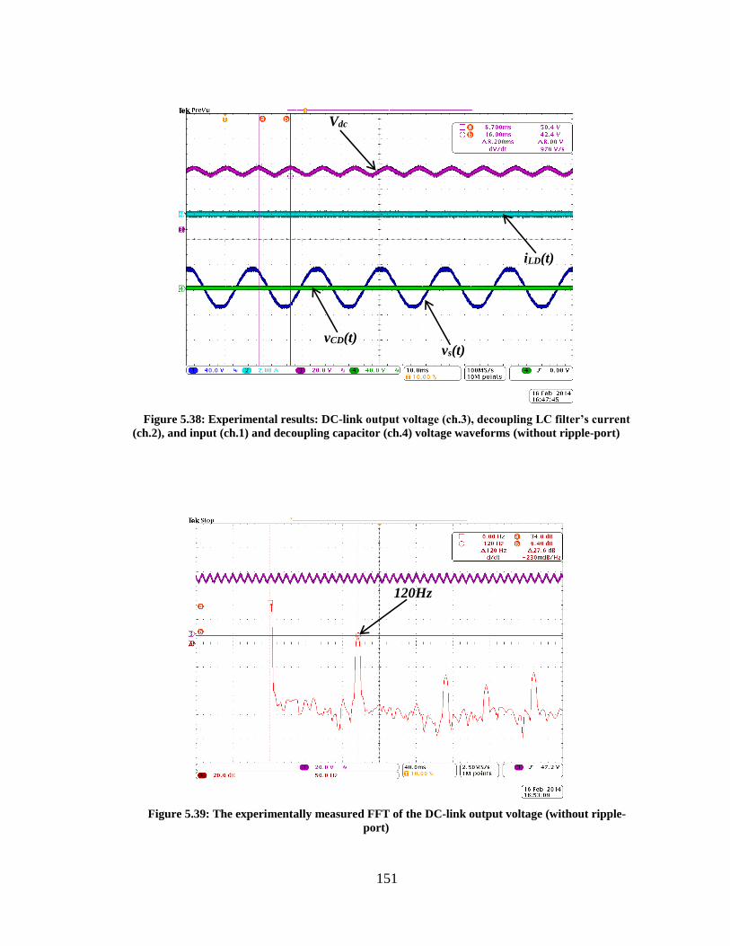
151
Figure 5.38: Experimental results: DC-link output voltage (ch.3), decoupling LC filter’s current
(ch.2), and input (ch.1) and decoupling capacitor (ch.4) voltage waveforms (without ripple-port)
Figure 5.39: The experimentally measured FFT of the DC-link output voltage (without ripple-
port)
vs(t) vCD(t)
iLD(t)
Vdc
120Hz

152
Table 5.9: Comparison of operating the AC/DC system with and without the ripple-port
DC voltage ripple
(ΔV)
120 Hz of DC port
current
120Hz relating to
DC
Ripple-port activated 1.4V -13.6 dB 47.2 dB
Ripple-port deactivated 8V 6.4 dB 27.6 dB
Ripple-port suppression 20 dB
5.3 Conclusion
The ripple-port concept, for double-line frequency ripple cancellation, is presented in
this section. It is implemented for both single-phase DC/AC inverter and AC/DC rectifier
applications. First, the proposed module-integrated inverter (MII) is based on the
commonly used two-stage inverter. A third port is added for ripple cancellation purposes;
it simply attached to the DC-Link. This implies that the ripple-port could be added to many
commercially available inverter topologies. Two configurations for implementing the
proposed MII were examined by simulation, and the best was experimentally tested.
Second, the ripple-port is connected to a single-phase AC/DC rectifier. Only 140µF is
needed as decoupling capacitance. Simulation and experimental results were presented
that proves the ripple cancellation concept without affecting the high performance of the
PWM rectifier. The results show that the ripple-port is completely independent of the type
of the AC/DC rectifier stage (PWM or diode bridge followed by boost PFC). For both
applications, a very small capacitance is required, where a high reliability film capacitor

153
can be used instead of the bulky, low reliability electrolytic ones. Consequently, the
system’s reliability and power density are improved. The ripple-port can be completely
designed and controlled independently of the main power stage design process.

154
6 DC-LINK BASED POWER DECOUPLING VERSUS THE RIPPLE-PORT
POWER DECOUPLING TECHNIQUES
In this section, the proposed ripple-port MII, Figure 6.1, is compared against the
conventional DC-link MII, Figure 6.2. In the conventional DC-link MII topology, the
decoupling capacitor can be placed either on the low-voltage PV side or on the relatively
high-voltage DC-link. In this study, the latter approach will be considered since less
decoupling capacitance is needed for the same power rating. Thus, a smaller capacitor can
be used. Yet, film capacitors are not a cost effective technology. More detail on the
feasibility and the cost effectiveness of film capacitors are discussed later in the section.
The aim of this comparative study is to thoroughly investigate the impact of the extra
components, due to the ripple-port, on the efficiency and the cost of the MII—given that
both topologies have the desired 25-year lifetime.
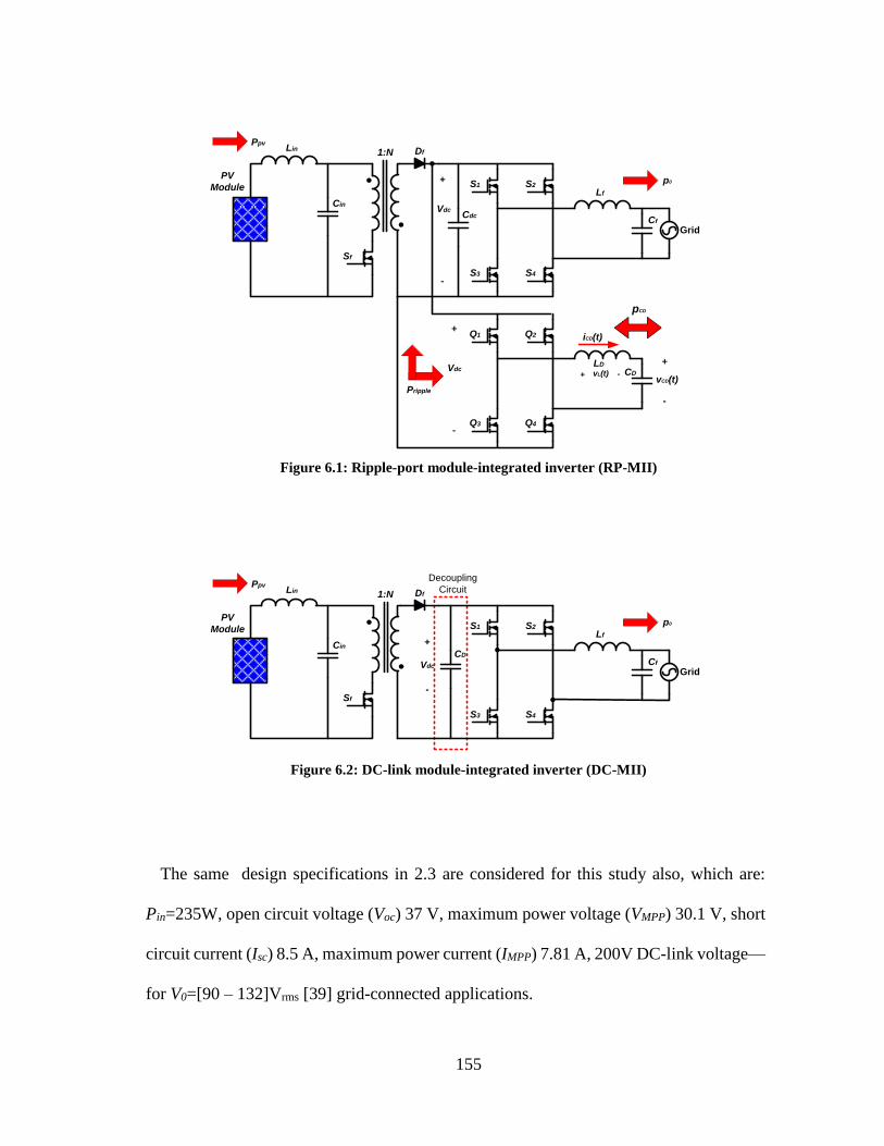
155
Figure 6.1: Ripple-port module-integrated inverter (RP-MII)
Figure 6.2: DC-link module-integrated inverter (DC-MII)
The same design specifications in 2.3 are considered for this study also, which are:
Pin=235W, open circuit voltage (Voc) 37 V, maximum power voltage (VMPP) 30.1 V, short
circuit current (Isc) 8.5 A, maximum power current (IMPP) 7.81 A, 200V DC-link voltage—
for V0=[90 – 132]Vrms [39] grid-connected applications.
GridCf
Lf
CD
LD
Cdc
Df
Cin
Lin
PV
Module
Sf
S1 S2
S3 S4
Q1 Q2
Q3 Q4
Ppv
p0
Pripple
1:N
Vdc
Vdc+
-
vCD(t)
iCD(t)
pCD
+
-
+
-
vL(t)+ -
GridCf
Lf
CD
Df
Cin
Lin
PV
Module
Sf
S1 S2
S3 S4
Ppv
p0
1:N
Vdc
+
-
Decoupling
Circuit

156
The rest of this section is organized as follows: First, both topologies are designed for
high-reliability in 6.1. Then, the efficiency calculations are presented in 6.2. In 6.3, the
price comparison is presented, and finally, a conclusion is drawn in 6.4.
6.1 Design for high-reliability
In this section, the required decoupling capacitance is calculated for both topologies.
Then, for the conventional DC-link MII topology, the decoupling capacitance is derated
in order to have a 25-year lifetime.
6.1.1 Design the decoupling capacitor for the conventional DC-link MII
This decoupling technique belongs to type IIa1, as shown in section 4, and the required
decoupling capacitance is calculated using (6.1). The capacitance value results from (6.1)
can be implemented using either electrolytic or film capacitor technology. However,
implementing this relatively large capacitance by film capacitor technology is not
practically feasible due to its high cost and large size. Hence, this decoupling capacitance
is implemented by electrolytic capacitor. The price and size of different capacitor options
are presented later in this section.
dcdc
inD
vV
PC ~
FCD 31210*200*377
235
(6.1)
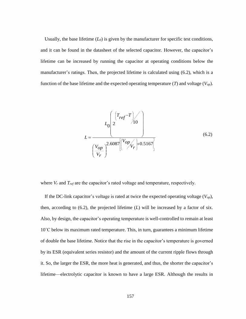
157
Usually, the base lifetime (L0) is given by the manufacturer for specific test conditions,
and it can be found in the datasheet of the selected capacitor. However, the capacitor’s
lifetime can be increased by running the capacitor at operating conditions below the
manufacturer’s ratings. Then, the projected lifetime is calculated using (6.2), which is a
function of the base lifetime and the expected operating temperature (T) and voltage (Vop).
5167.06087.2
1020
rVopV
rV
opV
Tref
T
L
L (6.2)
where Vr and Tref are the capacitor’s rated voltage and temperature, respectively.
If the DC-link capacitor’s voltage is rated at twice the expected operating voltage (Vop),
then, according to (6.2), the projected lifetime (L) will be increased by a factor of six.
Also, by design, the capacitor’s operating temperature is well-controlled to remain at least
10˚C below its maximum rated temperature. This, in turn, guarantees a minimum lifetime
of double the base lifetime. Notice that the rise in the capacitor’s temperature is governed
by its ESR (equivalent series resistor) and the amount of the current ripple flows through
it. So, the larger the ESR, the more heat is generated, and thus, the shorter the capacitor’s
lifetime—electrolytic capacitor is known to have a large ESR. Although the results in

158
[116] show that the capacitor’s temperature could reach as high as 100˚C, the
measurements in section 2 show that the module’s operating temperature was as high as
65˚C. Moreover, according to [22], the PV module was operating at temperatures less than
60°C for 95% of the time. Hence, it is a fair assumption that the capacitor’s maximum
temperature is 10˚C less than its rated one. Following these assumptions, the expected
lifetime is at least 12 times the base time, as shown in (6.3).
057.12
15907.0
02
LL
L (6.3)
However, using a capacitor with a rated voltage twice the maximum expected operating
voltage is definitely going to increase the cost. Moreover, operating the capacitor at a
temperature level with 10˚C lower than its rated temperature may need extra requirements.
For example, using a larger inductance results in a reduced current ripple, consequently,
lower temperature rise in the capacitor. However, this could increase the losses in the
inductor and the cost of the MII. Quantifying these practical techniques is beyond the
scope of this section.
Two electrolytic capacitors are considered as a case study, as shown in Table 6.1 [117,
118]. The purpose of this comparison is not to study the performance or the quality of
different manufacturers’ products rather than showing an actual lifetime calculations. Both
capacitors’ rated voltage is 450V. According to (6.3), option I and II, in Table 6.1, are

159
expected to last for 4.3 years and 7.17 years, respectively. Table 6.1 shows that option II
has a lifetime 1.66 times the lifetime of the first option. But, its price is 2.47 times the
price of option I. However, the lifetime is not the only thing that has improved in option
II; its operating temperature is 20˚C higher and its ESR is almost half the ESR of option
I.
Table 6.1: Two electrolytic capacitor options
Manufacturer Capacitance Base lifetime ESR Size Price ($)
I - Panasonic
Electronic -
Electrolytic
330µF 3,000 Hrs @
85°C 553 mΩ
30mm x 50mm
(D x H) 5.89
II - Vishay -
Electrolytic
330µF 5,000 Hrs @
105°C 300 mΩ
35mm x 40mm
(D x H)
14.56
EPCOS - Film 40µF 200,000 Hrs
@ VR, 85°C 1.9 mΩ
57.5mm x 30mm x 45mm
(LxWxH) 10.487
6.1.1.1 Derating the decoupling capacitor at the DC-link
It is required for the microinverter, built using the convention DC-link approach, to keep
performing and meet the design specifications, such as voltage ripple and THD. The
voltage ripple on the DC-link is directly related to the capacitance value. However, it is
well-known that the end of life for the aluminum electrolytic capacitor is determined by

160
one of the following factors: (1) capacitance decreases by at least 20%, (2) or the
dissipation factor (or ESR) increases by at least 300%. In this study, the change in the
electrolytic capacitor is considered as the main factor that determines its end of life, as
shown in Figure 6.3. Thus, this decrement in the capacitance needs be taken into account
and compensated for at the design stage by derating the required capacitance.
Figure 6.3: Pictorial illustration of the capacitance decrement with time
The desired capacitance (CD) that the MII needs to have by the end of its expected
lifetime is given in (6.4). In order to cancel the double-line frequency ripple, the designer
must make sure that at the end of the MII’s lifetime the decoupling capacitance matches
with (6.1). Then, the required initial capacitance (C0) can be calculated using (6.4), where
(n) is the ratio of the desired lifetime to the base lifetime given in (6.3).
t=0 t=L0 t=2L0 t=3L0 t=nL0
C=C0
C=kC0
C=k2C0
C=k3C0
C=knC0

161
oL
L
o
n
D CkCkCd
(6.4)
k=1-ΔC% is determined based on the allowed ripple on the DC-link that can be tolerated
without significantly affecting the MPPT performance as well as the THD of the injected
output current. However, the capacitor is considered to have a soft failure if its capacitance
decreased by 20% of its initial value [119]. Considering option II that has a longer lifetime
(62,850 hours), the initial capacitance (C0) is 1.863 times CD according to (6.4)—given a
20-year lifetime (175,200 hours). From (6.1), 312 µF is required for decoupling purposes.
Thus, C0=1.863*312µF=581.26µF. A 560µF capacitor from Nichicon
(LGX2G561MELC40) is considered with a base lifetime of 5,000 hours and $10.36 unit
price [120].
6.1.2 Design the decoupling capacitor for the DC-link based ripple-port MII
It was presented in section five that the decoupling capacitance for the DC-link ripple-
port MII is calculated as given in (6.5); and for the system’s specifications given in section
6.1, 40µF is needed, which can be implemented by film capacitor technology.
2
2
CDp
inD
V
PC
FCD 40180*377
235*22
(6.5)

162
Table 6.1 shows the main parameters for a film capacitor from EPCOS [121]. With
200,000 hours base lifetime, this capacitor is expected to last for more than 22 years if it
operates at the rated 85˚C temperature, which is not the case as it was explained previously
in this section. This suggests that a film capacitor can be designed to operate at the rated
conditions (voltage and temperature), yet, it will last for longer time compared to the
electrolytic capacitor. Moreover, the ESR of the electrolytic capacitor is at least 100 times
larger than the film capacitor one.
6.1.2.1 Multiple capacitor in parallel option
Paralleling number of capacitors with smaller capacitance is a very common engineering
practice mainly to reduce the equivalent ESR, which will be divided by the number of
capacitors. Hence, the calculated decoupling capacitor for both approaches (electrolytic
and film approaches) will be implemented by four paralleled capacitors. Table 6.2 lists the
main parameters of each selected capacitor. However, in aluminum electrolytic capacitor
technology, the ESR is a function of the capacitance and the operating frequency, as given
in (6.6). This means that when a small capacitance is used, its ESR is expected to be
relatively larger. For example, if a 150 µF capacitor is considered, its ESR is 910m Ω,
which is almost three times of the larger capacitor (560 µF).
fC
DFESRfCESRDF
22tan
(6.6)

163
Table 6.2: Parallel capacitors option
Manufacturer Capacitance Base lifetime ESR Size Price ($)
EPCOS Inc
(B43505A5157M) 150µF
5000 Hrs @
105°C 910m Ω
30mm x 35mm
(DxH) 5.55x4
EPCOS Inc
(B32676E4106K) 10µF
200,000 Hrs
at VR, 85 °C 7.3m Ω
42mm x 20mm x
39.50mm (LxWxH) 3.88x4
Figure 6.4: Aluminum electrolytic and metalized polypropylene film capacitors – comparison
6.1.3 Electrolytic versus film capacitor
Many studies have been published recently on the reliability of the DC-link capacitor
and the technology used to enhance the inverter’s performance as well as reliability [122,
123]. In [122], a detailed analysis on designing the DC-link capacitor for high-reliability
is presented. Failure modes and mechanisms for three capacitors’ technologies (aluminum
electrolytic, metalized polypropylene film, and multi-layer ceramic capacitors) are
42mm
20mm
39.5mm30mm35mm
Aluminum Electrolytic Capacitor
C=150µF, ESR=910m Ω
Metalized Polypropylene Film Capacitor
C=10µF, ESR=7.3m Ω

164
investigated in the study [122].
The aluminum electrolytic capacitor has high energy density at low cost, but at the
expense of relatively high ESR, low current ripple capability, and relatively short lifetime
due to evaporation of electrolyte. On the other hand, metalized polypropylene film
(MPPF) capacitor shows superiority in terms of current ripple capability and low ESR.
However, it suffers from a low energy density (large size) and moderate operating
temperature [122]. Moreover, the self-healing capability of the MPPF capacitor makes it
an attractive option when compared to aluminum electrolytic capacitor.
6.2 Efficiency calculation
In this section the power loss due to the added component in each MII topology is
examined. For the conventional DC-link MII, the added power loss is due to the derated
DC-link capacitor. And, for the proposed DC-link ripple-port, the power loss is due to the
added H-Bridge (4 MOSFETs) and the decoupling LC filter.
6.2.1 DC-link current
IC,rms is the rms (root mean square) value of the current ripple flows in the DC-link
capacitor. ICrms is needed to calculate the power loss in the DC-link capacitor’s ESR. The
inverter’s input current is needed to calculate the power loss in the H-Bridge’s MOSFETs.
The DC-link capacitor’s current is a function of the output current of the input DC/DC
stage (idc0) and the H-Bridge inverter’s current (iinv) as given in (6.7).

165
)()(0
)( tinvitdc
itDC
Ci
rmsinvIrmsdc
Irms
DCC
I ,,0,
(6.7)
idc0 depends on the type of the DC/DC stage, however, for PV-MII applications, it should
be a boost-type converter. Considering the most common flyback topology, the output
current is given in (6.8).
2
/
/,0 *1
mmp
DCDCs
p
DCDCrmsdc IDN
NDI (6.8)
The inverter’s input current can be calculated as shown in (6.9), using the H-Bridge’s
output voltage from [124].
)(1
)()(
)( 0
0
2
0
0
0
0
00 tv
RsLsCLR
sCRti
Z
tvti B
fff
fB
tntcmnmm n
Mmnj
m
DCVtMDCVtBv 0122cos1cos
112
2
18
0cos2)(0
(6.9)
Considering a lossless system, the rms value of the inverter’s input current is calculated
as follows:
166
0PPDC
rmsI
rmsBVrmsinvI
DCV
,0,0,
DCV
rmsI
rmsBV
rmsinvI,0,0
,
(6.10)
6.2.2 DC-link MII
Because of the derated DC-link capacitor’s ESRCD, this approach will experience more
power loss in the form of dissipated heat. It is very important to precisely calculate the
power loss due to the ESRCD not only to estimate the system’s efficiency, but also to
calculate the increment in the capacitor’s operating temperature, as given in (6.11). This
increase in the operating temperature will potentially decrease the capacitor’s expected
lifetime according to (6.2).
ACthRCDESRrmsCIAT
ACthR
lossPATCDT
**
2,*
(6.11)
This power loss is calculated using (6.12).
CDESRrmsCIloss
P *2
, (6.12)

167
6.2.3 DC-link based ripple-port MII
The power loss due to the extra H-Bridge (four MOSFETs) and the decoupling LC filter
is calculated. However, the dominant power loss is due to the MOSFETs since they are
hard-switched. The power loss in MOSFETs can be estimated following the analysis in
[125]. The main power loss equations, for a PWM controlled single-phase inverter, are
presented next.
6.2.3.1 Conduction power loss
The power loss in the tipple-port’s H-Bridge is divided into conduction and switching
losses. The conduction losses in MOSFET and its body diode are given in (6.13) and
(6.14), respectively.
cos
38
1*** 2
0
2
,_
MIRIRP ONDSrmsDONDSMOSC (6.13)
cos
38
1*
20*cos
82
1*0*0
2,**0_
MIDR
MIDvrmsFIDRFavIDvDiodeCP (6.14)
6.2.3.2 Switching power loss
Table 6.3 shows how to calculate the energy loss due to turning ON and OFF the
MOSFET. Because the drain-source voltage nonlinearly depends on the MOSFET’s
output capacitance, the two-point approximation is used to estimate the rise and falling
168
time of the drain-source voltage, as shown in Table 6.3 [125]. In the PWM AC power loss
calculation, the ID,ON and ID,OFF can be considered to equal the average value of the output
current over a half link cycle
0,,
I
OFFDIONDI
Table 6.3: Switching power loss calculations
Device Switching losses
MOSFET
SW
fMOSOFF
EMOSON
EMOSSW
P *,,_
where
DCVrrQfv
trit
ONDIDCVMOSONE *2
*,*,
2*,*,
fitrvt
OFFDIDCVMOSOFFE
plateau
V
GDC
GRONDIONDSRDCVrvt
plateauV
GDC
GRONDIONDSRDCVrvt
rvtrvt
rvt
plateauVGV
GDC
GRONDIONDSRDCVfv
t
plateauVGV
GDC
GRONDIONDSRDCVfv
t
fvt
fvt
fvt
2**,*2
1**,*1
2
21
2**,*2
1**,*1
2
21
Diode
SWf
DiodeONESWf
DidoeOFFE
DiodeONE
DiodeSWP *
,*
,,_
DCVrrQDidoeON
E **4
1
,

169
6.3 Comparison
The price and power loss, due to the capacitor’s ESR, of each approach are presented in
this section. Table 6.4 shows the volume, power loss, and price of both the electrolytic
and film capacitors. It shows that the film capacitor approach results in 26% increase in
the volume. However, film capacitor approach turned out to be 30% less expensive.
Table 6.4: Paralleled capacitors implementation comparison
Volume Power loss Price ($)
Electrolytic capacitors 4x24.74cm3=99cm3 278.8 mW 22.2
Film Capacitor 4x33.18cm3=134.4cm3 6.73 mW 15.52
Table 6.5 shows the distribution of the power losses in one MOSFET, which conclude
that an H-Bridge (four MOSFETs) will have a total power loss (Ptotal) of 18.73 W. This
translates into 7.97%. However, Table 6.5 shows that the dominant cause of the power
losses in MOSFET occurs at the turn ON instant. It accounts for 68% of the total power
loss, as shown in Figure 6.5. The root cause of this power loss is the reverse recovery in
the boy diode. Hence, in order to improve the performance of the ripple-port, the losses
due to the reverse recovery need to be suppressed. One simple and straightforward
approach is to use new semiconductor MOSFET, such as SiC or Gan. Also employing

170
zero voltage switching (ZVS) technique can completely eliminate the turn ON losses.
Table 6.5: MOSFET power loss
Conduction
Loss
Switching Loss Total loss
by device Turn ON Turn OFF Total
MOSFET 0.3384 3.1709 0.2978 3.4687 3.8071
Body Diode 0.1254 0.75 0.8754
Total power loss 0.4638 4.2187 4.6825
Figure 6.5: MOSFET's power losses distribution
7%
68%
6%
3% 16%
MOSFET's Power Loss
Distribution
PC_MOS
Psw_MOS_ON
Psw_MOS_OFF
PC_Diode
Psw_Diode
171
6.4 Conclusion
The proposed DC-link based ripple-port PV-MII topology, which is presented in section
five, was compared to the conventional DC-link based inverter in this section. For a 20
years lifetime, the efficiency, size, and price of both configurations were presented. It was
found that the proposed ripple-port topology is competitive with the conventional
topology in terms of size and price. Although the film capacitor approach results in 26%
increase in the volume, it turned out to be 30% less expensive. Given the current
semiconductor devices state, there is approximately 8% power loss due to the extra four
switches introduced by the proposed ripple-port (H-Bridge). However, 68% of these
power losses can be eliminated by either using a new semiconductor technology (GaN,
SiC) or employing ZVS technique.
172
7 AC-LINK BASED RIPPLE-PORT *
7.1 High-frequency AC-link MII
In the section V, the impact of the number of capacitors on the reliability was presented.
In addition to reducing the value of the decoupling capacitance, reducing the number of
the capacitors will decrease the failure rate of the inverter. Another way to implement the
ripple-port concept is by attaching it to a multi-stage inverter at a high-frequency AC link.
Figure 7.1 shows a general block diagram of the proposed AC-link based ripple-port. As
it was presented in section 5, the proposed technique can be applied for both DC/AC and
AC/DC power conversion applications. In this section, it will be implemented for PV-MII
application. The proposed MII can be implemented in two different topology
configurations, based on the way that the ripple-port is added to the inverter: a separated
ripple-port shown in Figure 7.2 or an integrated ripple-port shown in Figure 7.3. By
controlling the power flow at the AC-link the double-frequency ripple from the grid-
connection is prevented from propagating to the PV module on the dc port. This improves
energy harvest as it was illustrated in section four. When the input power from the PV
module is greater than the instantaneous output power to the utility the extra power is
stored in the decoupling capacitor. This power will be transferred into the output side (grid
utility) when the input PV power is lower than the output grid. Figure 7.3 shows how the
* © 2013 IEEE. Reprinted, with permission, from S. Harb, H. Zhang, and R.S. Balog, “AC-Link, Single-
phase, Photovoltaic Module Integrated Inverter,” 28th Annual IEEE Applied Power Electronics Conference
and Exposition (APEC), March, 2013.

173
ripple-port can be coupled to the ac-link in the main circuit topology by adding an
additional transformer winding, which gives the designer the ability to control the input
voltage of the ripple-port by adjusting the turn’s ratio. This degree of freedom in the design
of ripple-port, however, increases the complexity of the transformer design [126].
Figure 7.1: A general system block diagram of AC-link based ripple-port
Figure 7.2: AC link ripple-port concept – separate winding configuration
DC
Device
DC/AC
Converter
AC/AC
Converter
AC/AC
Converter
AC side
Filter
Ripple-port
FilterStorage
AC
Device Filter
DC Port AC Port
Ripple-Port
AC-Link
AC/DC Rectifier
DC/AC Inverter
Power flow
Power flow
Grid
CD
High-frequency
Link
AC/AC
Double-freq.
Ripple-portHigh-frequency
Link
AC/AC
DC/AC
Inverter
PV-Module
Pin P0
Pripple

174
Another approach for implementing the ripple-port is by integrating it to the secondary
side of the transformer as shown in Figure 7.3. Although a simpler transformer design,
integrating the ripple-port constrains the input voltage of the ripple port to be equal to the
input voltage of the high frequency link output converter, which is governed by the grid
voltage. In either case, the DC/AC stage on the PV-side generates a high frequency bipolar
square wave for efficient use of the magnetic core and can be implemented with either a
push-pull or a full-bridge based converter as shown in Figure 7.4.
Figure 7.3: AC link ripple-port concept – integrated single winding
Figure 7.4: Two possible converters for DC/AC stage at the PV-side
Grid
Double-freq.
Ripple-port
DC/AC
Inverter
PV-Module
CDHigh-frequency
Link
AC/AC
High-frequency
Link
AC/AC
Pin
Pripple
P0
S2S1
S3 S4S1S2
(b) Full-bridge(a) Push-pull

175
7.1.1 Integrated ripple-port MII implementation (i-RP-MII)
Figure 7.5 shows the implementation of the integrated ripple-port configuration. The
full-bridge is switching at fs1 with a duty ratio of half. Both high-frequency link AC/AC
converters, on the secondary side, are switching at fs2, which has to be faster than fs1
(multiple of fs1). Bidirectional switches are used for both converters to provide a
bidirectional current path. Two bidirectional switch configurations are shown in Figure
7.6. The common-source ac switch enables the same gate drive signal to be applied to both
MOSFETs, which reduces the requirements for high-side isolated gate drives. However,
applying the same gate signal for both MOSFTs implies a hard switching, which means
that snubber circuits are needed to prevent damaging the MOSFETs. Hence, extra cost and
higher power losses. In practice an external anti-parallel Schottky diode may be used to
achieve lower losses. Another approach of switching the bidirectional switches, in high-
frequency AC/AC converter, is “four-step switching” technique [127, 128], which
guarantees to provide a path for the output current during the commutation period while
eliminating the need for snubber circuit. It also provides partial soft switching. This
switching technique is thoroughly presented later in this section.

176
Figure 7.5: AC-link based inverter with an integrated ripple-port
Figure 7.6: Bidirectional switch configuration: (a) common-source, (b) common-drain
configurations
7.1.2 Controlling the HF link PWM inverters
The gate signals that control both high-frequency link AC/AC converters are generated
as shown in Figure 7.7. V0ref is the output voltage reference, and Vripple-ref is the voltage
across the decoupling capacitor reference, which has the amplitude and phase angle as
shown in (5.9) and (5.10).
GridCf
Lf
CD
PV-Module
LD
S2S1
S3 S4
Q4
Q1 Q2
Q3
Q42
Q41
VS
Pin P0
Pripple
Q5 Q6
Q7 Q8
1:N
(a) (b)

177
Figure 7.7: Control Circuit: high-frequency AC/AC converter driving signals generation
7.2 Controlling the bidirectional AC/AC H-Bridge
Table 7.1 shows all the possible static switch states for the high-frequency AC/AC
converter shown in Figure 7.5. The polarity of the load current does not affect the static
switch states, which are: State 1 when Q1, Q4 are ON and State 2 when Q2, Q3 are ON. For
each state, there are two possible conditions that determine the static conduction state, as
shown in Figure 7.8. The transitions between these conduction states are pictorially
presented in Figure 7.9, which shows when the transitions happen.
Table 7.1: All possible static switch states
iLoad VLink PWM Switch ON
+ + High Q1, Q4
+ + Low Q2, Q3
+ - High Q2, Q3
+ - Low Q1, Q4
- + High Q1, Q4
- + Low Q2, Q3
- - High Q2, Q3
- - Low Q1, Q4
+
-
+
-
+
-
Vs
0
V0ref
Vsaw Output
PWM signal
Q1&Q4
Q2&Q3
Q5&Q8
Vripple-ref
Vsaw Ripple-port
PWM signal
Secondary voltage sign
Q6&Q7XOR XOR
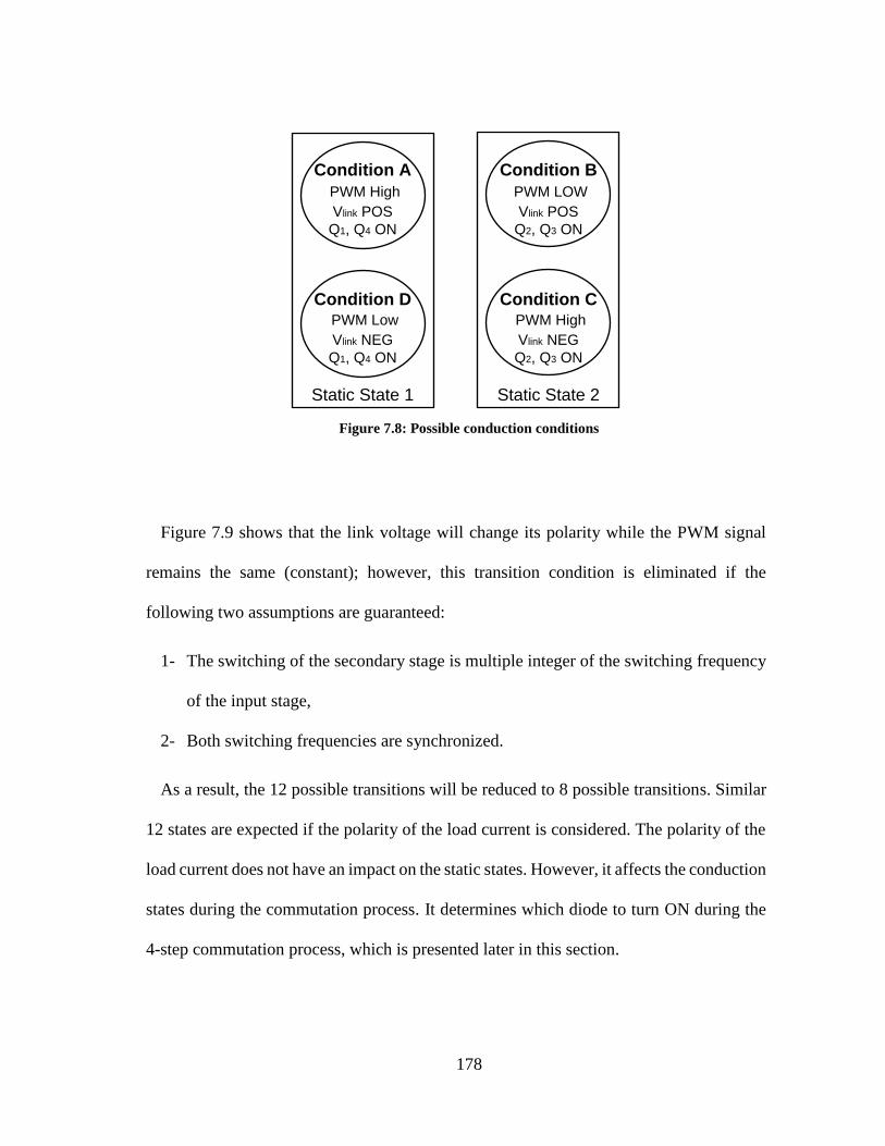
178
Figure 7.8: Possible conduction conditions
Figure 7.9 shows that the link voltage will change its polarity while the PWM signal
remains the same (constant); however, this transition condition is eliminated if the
following two assumptions are guaranteed:
1- The switching of the secondary stage is multiple integer of the switching frequency
of the input stage,
2- Both switching frequencies are synchronized.
As a result, the 12 possible transitions will be reduced to 8 possible transitions. Similar
12 states are expected if the polarity of the load current is considered. The polarity of the
load current does not have an impact on the static states. However, it affects the conduction
states during the commutation process. It determines which diode to turn ON during the
4-step commutation process, which is presented later in this section.
PWM High
Condition A
Vlink POS
Q1, Q4 ON
PWM Low
Vlink NEG
Q1, Q4 ON
PWM LOW
Vlink POS
Q2, Q3 ON
PWM High
Vlink NEG
Q2, Q3 ON
Static State 1 Static State 2
Condition B
Condition D Condition C

179
Figure 7.9: The transitions between the conduction states
7.2.1 Multi-step commutation
In the conventional H-Bridge, the body diodes provide a conduction path for current ro
flow when the MOSFET is turning off. However, for the bidirectional H-Bridge, two
MOSFETs are connected in series (common-source) in order to provide the bidirectional
A-1 B-2
B-2 D-1
Vlink POS
PWM
VLink
PWM LowA-1
A-1
C-2
D-1
B-2
B-2
A-1
C-2
C-2
C-2
C-2
A-1
D-1
B-2
D-1
D-1
D-1
C-2
B-2
A-1
PWM
VLink
VLink
PWM High
PWM
Vlink POS
PWM
VLink
Vlink NEG
PWM
PWM High
VLink
VLink
PWM
Vlink NEG
PWM
PWM Low
VLink
VLink
PWM

180
current flow and voltage blocking capability. However, when the switches Q1 and Q4 in
Figure 7.5 are turned OFF, there will be no path for the current to flow, since the body
diodes of Q2 and Q3 will block it. Hence, this will result in a huge voltage spike across the
MOSFETs, which can damage them if not snubbed or clamped. So, a path for this current
must be provided during the switches commutation. Conventionally, dissipative snubber
circuits are used across each switch. In addition of extra cost of this solution, it also
increases the power losses, and, as a result, decreases the overall converter efficiency.
Alternatively, the four-step switching control technique [127-129] is a make-before-break
switching strategy that establishes an incoming path for the output current before breaking
the outgoing path. No extra components are needed by the four-step switching technique.
And soft-switching may be possible under the right conditions, as it will be shown later in
this section. Hence, lower power loss and higher efficiency. Thus, it will be employed to
control the commutation of the secondary stage of the AC-link MII proposed in this
section.
Figure 7.10 is a moore state machine representation that shows all the possible
transitions and the commutation processes. The turned ON switches, due to the
corresponding action, are indicated in black color, while the conducting switches are
indicated in light gray. It shows that the 8 possible state transitions, shown in Figure 7.9,
are reduced to only 4 state transitions. For the remaining 4 state transitions, the PWM
signal acts as triggering signal that starts the current commutation process as shown in
Figure 7.10. The detailed circuit schematics for these 4 state transitions are shown in
Figure 7.11 and 7.12.

181
Figure 7.10: All possible transitions and the commutation process
Figure 7.11 shows the current commutation when switching from Q1, Q4 to Q2, Q3, in
the case of positive link voltage. The four-step commutation process starts by turning ON
Q2b and Q3b in step-1, and then, Q1a and Q4a are turned OFF in step-2. If the output current
Q1a, Q1b
Q4a, Q4b
Q1a, Q1b
Q4a, Q4b
Q2b, Q3b
Q1b, Q4b
Q2b, Q3b
D2a, D3a
Q1b, Q4b
Q2a, Q2b
Q3a, Q3b
Q2a,Q2b
Q3a, Q3b
Step-2
Step-3
Delay=0s
Delay=200ns
Delay=200ns
Step-4
Delay=200ns
Delay=0s
Q1b, Q4b
Q2b, Q3b
D1a, D4a
Step-2Delay=200ns
Step-3Delay=200ns
Step-4Delay=200ns
Q1a, Q1b
Q4a, Q4b
Q2a, Q3a
Q1a, Q4a
Q2a, Q3a
D1b, D4b
Q1a, Q4a
Q2a, Q2b
Q3a, Q3b
Step-2
Step-3
Delay=0s
Delay=200ns
Delay=200ns
Step-4Delay=200ns
Delay=0s
Q2a, Q3a
Q1a, Q4a
D2b, D3b
Step-2Delay=200ns
Step-3Delay=200ns
Step-4Delay=200ns
Static state 2
Static state 1
i0>0 i0<0 i0>0 i0<0
PWMPWM
PWMPWM
Bè
A
Dè
C
Vlink POS
DèA
AèD
BèCCèB
Vlink POS Vlink NEG
Cè
D
Vlink NEGAè
B
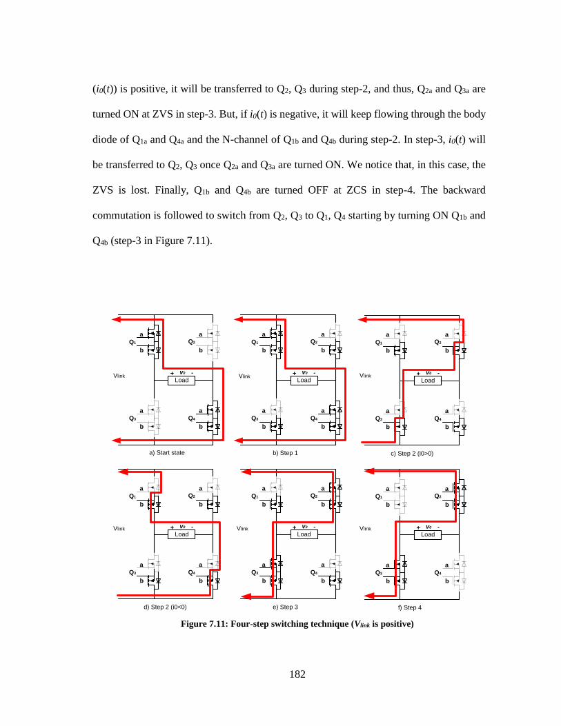
182
(i0(t)) is positive, it will be transferred to Q2, Q3 during step-2, and thus, Q2a and Q3a are
turned ON at ZVS in step-3. But, if i0(t) is negative, it will keep flowing through the body
diode of Q1a and Q4a and the N-channel of Q1b and Q4b during step-2. In step-3, i0(t) will
be transferred to Q2, Q3 once Q2a and Q3a are turned ON. We notice that, in this case, the
ZVS is lost. Finally, Q1b and Q4b are turned OFF at ZCS in step-4. The backward
commutation is followed to switch from Q2, Q3 to Q1, Q4 starting by turning ON Q1b and
Q4b (step-3 in Figure 7.11).
Figure 7.11: Four-step switching technique (Vlink is positive)
a
b
a
b
a
b
a
b
Load
v0+ -
Q1 Q2
Q3 Q4
Vlink
a
b
a
b
a
b
a
b
Load
v0+ -
Q1 Q2
Q3 Q4
a
b
a
b
a
b
a
b
Load
v0+ -
Q1 Q2
Q3 Q4
a
b
a
b
a
b
a
b
Load
v0+ -
Q1 Q2
Q3 Q4
a
b
a
b
a
b
a
b
Load
v0+ -
Q1 Q2
Q3 Q4
a
b
a
b
a
b
a
b
Load
v0+ -
Q1 Q2
Q3 Q4
a) Start state b) Step 1 c) Step 2 (i0>0)
d) Step 2 (i0<0) e) Step 3 f) Step 4
Vlink Vlink
Vlink Vlink Vlink

183
Similarly, Figure 7.12 shows the switching from Q1, Q4 to Q2, Q3, but in the case of
negative link voltage. The four-step commutation process starts by turning ON turning
ON Q2a and Q3a, and then, Q1b and Q4b are turned OFF in step-2. If the output current (i0(t))
is negative, it will be transferred to Q2, Q3 during step-2, and as a result, Q2b and Q3b are
turned ON at ZVS. But, if i0(t) is positive, it will keep flowing through the N-channel of
Q1a and Q4a and the body diode of Q1b and Q4b during step-2. In step-3, i0(t) will be
transferred to Q2, Q3 once Q2b and Q3b are turned ON—the ZVS is lost. Finally, Q1a and
Q4a are turned OFF at ZCS during step-4. The backward commutation is followed to
switch from Q2, Q3 to Q1, Q4 starting by turning ON Q1a and Q4a (step-3 in Figure 7.12).

184
Figure 7.12: Four-step switching technique (Vlink is negative)
7.3 Efficiency and reliability
Although the extra switches needed in the proposed topologies add power losses,
holistically there are system benefits that outweigh these losses. Further, emerging, post-
silicon power semiconductor technologies, such as: SiC and GaN are capable of reducing
power losses by 70% to 80% [130]. Thus the issue of losses in the extra switches is
minimized and must be weighed against the added advantages gained in the flexibility and
capability of the circuit.
a
b
a
b
a
b
a
b
Load
v0+ -
Q1 Q2
Q3 Q4
a
b
a
b
a
b
a
b
Load
v0+ -
Q1 Q2
Q3 Q4
a
b
a
b
a
b
a
b
Load
v0+ -
Q1 Q2
Q3 Q4
a
b
a
b
a
b
a
b
Load
v0+ -
Q1 Q2
Q3 Q4
a
b
a
b
a
b
a
b
Load
v0+ -
Q1 Q2
Q3 Q4
a
b
a
b
a
b
a
b
Load
v0+ -
Q1 Q2
Q3 Q4
a) Start state b) Step 1 c) Step 2 (i0>0)
d) Step 2 (i0<0) e) Step 3 f) Step 4
Vlink Vlink Vlink
Vlink Vlink Vlink

185
Although, a partially soft switching is provided by the aforementioned four-step
switching technique, employing full soft switching techniques is another option that will
further reduce the power losses associated with the MOSFET. On the other hand, the
overall reliability of the MII is improved by using a highly reliable film capacitor.
Moreover, it has to be stressed that the DC-link capacitor is completely eliminated.
Consequently, the reliability is further improved as shown in [131].
7.4 Simulation results
PSIM was used to simulate the RP-MII. Table 7.2 shows the values of components that
are used in the simulation. Lin and Cin are the input filter, which filters out the high
frequency ripple.
Table 7.2: Simulation parameters
Component Value Component Value
Vin 30Vdc Lin 5mH
V0 120Vrms Cin 1000µF
fs1 6KHz Lf 10mH
fs2 18KHz Cf 10µF
N1:N2 1:12 Ld 200µH
R0 60Ω Cd 40µH
Figure 7.13 and Figure 7.14 show the gate signals of the output AC/AC converter during
the four-step commutation process. Figure 7.13 shows the gate signals when Vlink is

186
positive, while Figure 7.14 shows the case when Vlink is negative.
Figure 7.13: Current commutation when switching from Q1, Q4 to Q2, Q3 (Vlink is positive)
Figure 7.14: Current commutation when switching from Q2, Q3 to Q1, Q4 (Vlink is negative)
0.0
0.20
0.40
0.60
0.80
1.00
pwm0_1
0.0
0.20
0.40
0.60
0.80
1.00
14a 14b
431896.25 431897.50 431898.75 431900.00
Time (us)
0.0
0.20
0.400.60
0.80
1.00
23a 23b
PWM
Q2b, Q2b
Q1b, Q4bQ1a, Q4a
Q2a, Q2a
t0 t1 t2 t3
0.0
0.32
0.64
0.96
pwm0_1
0.0
0.20
0.40
0.60
0.80
1.00
14a 14b
425290.00 425290.50 425291.00 425291.50 425292.00 425292.50
Time (us)
0.0
0.20
0.40
0.60
0.80
1.00
23a 23b
PWM
Q1b, Q4bQ1a, Q4a
Q2b, Q2b Q2a, Q2a
t0 t1 t2 t3

187
The output (grid) voltage, v0, and the decoupling capacitor voltage, vCD are shown in
Figure 7.15. The timing between the grid voltage and the decoupling capacitor, shown in
Figure 7.15, is 2.27ms which corresponds to a phase difference is ϕ=49.032°. It is slightly
higher than the 45° degree derived in [132] due to the presence of the phase shift of the
grid-coupling LC filter and the inductor in the ripple-port. While this converter design has
not been optimized for efficiency, this performance is favorable compared to other film-
capacitor-based designs in the literature [39, 44]. Figure 7.16 shows the input, output, and
ripple-port power waveforms. It is clear in Figure 7.16 that whenever the input power is
greater than the instantaneous output power (p0(t)<Pin), the difference will be charging the
decoupling capacitor. And, the decoupling capacitor will discharge this power into the
output during the opposite state (p0(t)>Pin).
Figure 7.15: The output voltage, v0, and the voltage across the decoupling capacitor, vCD
460.00 480.00 500.00 520.00
Time (ms)
0.0
-100.00
-200.00
100.00
200.00
V0 VCd
ϕ
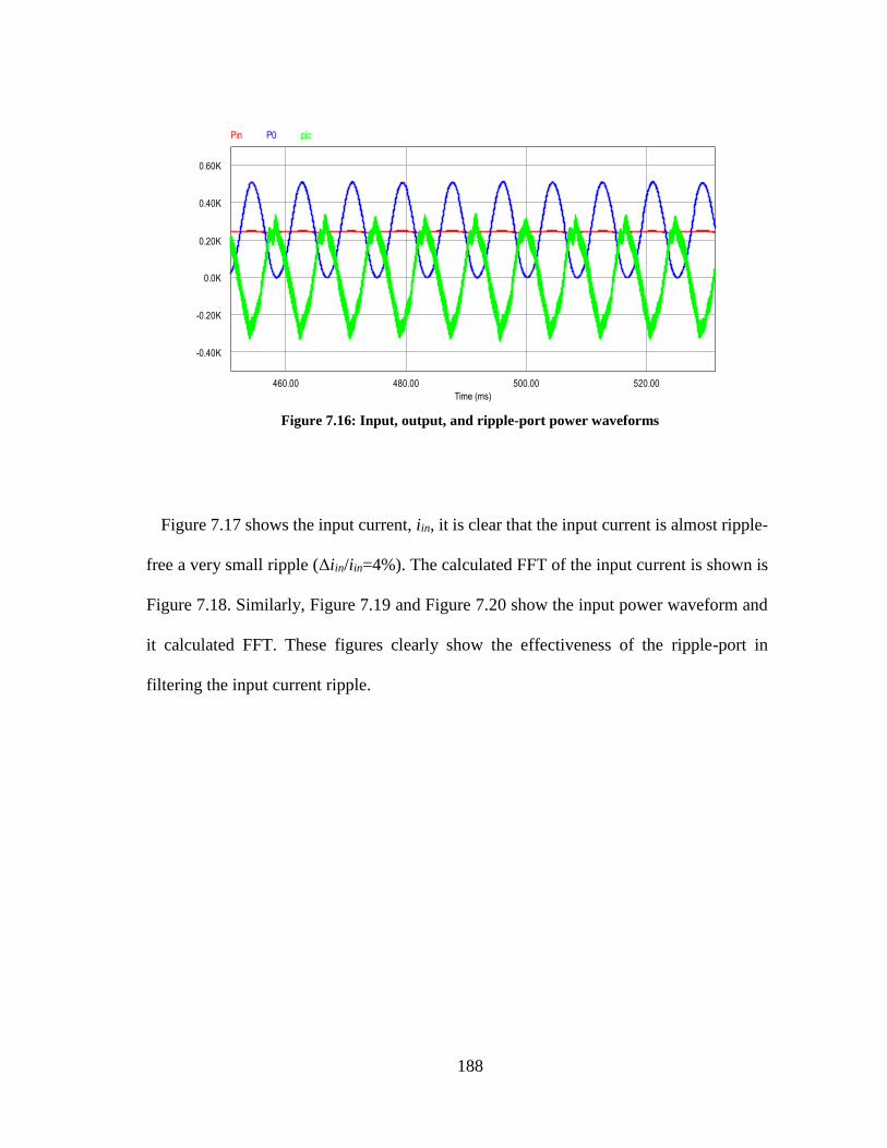
188
Figure 7.16: Input, output, and ripple-port power waveforms
Figure 7.17 shows the input current, iin, it is clear that the input current is almost ripple-
free a very small ripple (Δiin/iin=4%). The calculated FFT of the input current is shown is
Figure 7.18. Similarly, Figure 7.19 and Figure 7.20 show the input power waveform and
it calculated FFT. These figures clearly show the effectiveness of the ripple-port in
filtering the input current ripple.
460.00 480.00 500.00 520.00
Time (ms)
0.0K
-0.20K
-0.40K
0.20K
0.40K
0.60K
Pin P0 plc
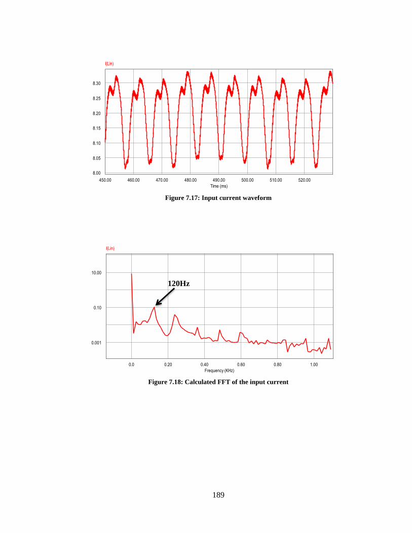
189
Figure 7.17: Input current waveform
Figure 7.18: Calculated FFT of the input current
450.00 460.00 470.00 480.00 490.00 500.00 510.00 520.00
Time (ms)
8.00
8.05
8.10
8.15
8.20
8.25
8.30
I(Lin)
0.0 0.20 0.40 0.60 0.80 1.00
Frequency (KHz)
0.001
0.10
10.00
I(Lin)
120Hz

190
Figure 7.19: Input power waveform
Figure 7.20: Calculated FFT of the input power
460.00 480.00 500.00 520.00
Time (ms)
242.00
244.00
246.00
248.00
250.00
Pin
0.0 0.20 0.40 0.60 0.80
Frequency (KHz)
1.00e-005K
0.001K
0.10K
Pin
120Hz

191
7.5 Experimental implementation and practical limitations
The proposed MII was prototyped for proof of operation concept, and the experimental
setup is shown in Figure 7.21. A constant DC voltage is used to represent a PV module
operating at MPPT. Figure 7.21 shows that both the AC-output and the ripple-port stages
are implemented using the same board construction. This illustrates the modularity of
implementing the proposed ripple-port concept.
Figure 7.21: Experimental setup of the proposed topology - PV-mode operation
Resistive Load
High-Frequency
Transformer
DC -Input
Voltage
AC
-O
utp
ut
sta
ge
Input stage
H -Bridge
Micro-Controller
Ripple -Port
stage

192
7.5.1 Preliminary experimental results
The proposed AC-link ripple-port MII, shown in Figure 7.21, was operated and tested
at low power level (Vin=10V, Iin=3.5A, R0=70Ω). The experimentally measured FFT for
the input DC current without the ripple-port is shown in Figure 7.22 that clearly shows a
high double-line frequency (120Hz) component. Then, the ripple-port was included, and
the result (measured FFT) is shown in Figure 7.23. The ripple-port is capable of
suppressing the 120Hz component. Figure 7.24 shows the output and the decoupling
capacitor’s voltage waveforms.
Figure 7.22: Measured FFT of the Input
current without the ripple-port
Figure 7.23: Measured FFT of the Input
current with the ripple-port
120Hz 120Hz
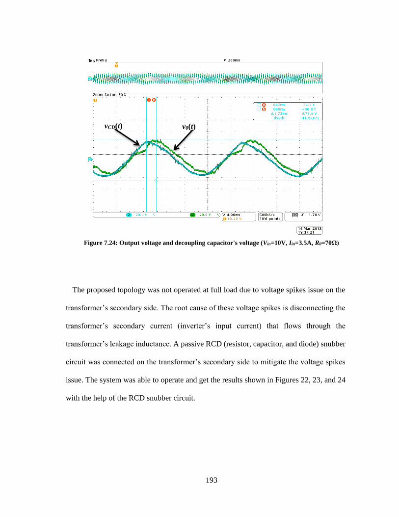
193
Figure 7.24: Output voltage and decoupling capacitor's voltage (Vin=10V, Iin=3.5A, R0=70Ω)
The proposed topology was not operated at full load due to voltage spikes issue on the
transformer’s secondary side. The root cause of these voltage spikes is disconnecting the
transformer’s secondary current (inverter’s input current) that flows through the
transformer’s leakage inductance. A passive RCD (resistor, capacitor, and diode) snubber
circuit was connected on the transformer’s secondary side to mitigate the voltage spikes
issue. The system was able to operate and get the results shown in Figures 22, 23, and 24
with the help of the RCD snubber circuit.
v0(t) vCD(t)

194
7.5.2 Practical limitation
When operating the high-frequency AC/AC converter, voltage spikes across the link
occurred at the link voltage polarity and AC/AC converter PWM transitions. Since the
transformer has a relatively large turn ratio (1:10), which is needed for PV-MII
applications, the reflected leakage inductance on the secondary side will be relatively large
(100 times the primary leakage inductance) even though the transformer has a very good
design with small primary leakage inductance.
7.5.2.1 Passive snubber circuit
A passive snubber circuit is used in order be able to operate the system. The simple
capacitive snubber circuit, shown in Figure 7.25, is very common practice in the
conventional DC-link inverter topology. However, for the AC/AC inverter topology, it
will create another problem and will not help. Because the capacitor is connected directly
across the AC-link that switches its voltage polarity, there will be a huge current spike
through snubber capacitor. The RCD snubbing approach is shown in Figure 7.26.
Including this snubber circuit on the transformer secondary side (AC-link) is able to
reduce the voltage spikes to an acceptable level that is not the breakdown voltage of the
MOSFETs neither the snubber diode. However, Snubber circuit are lossy solution and not
advantageous. Figure 7.26 shows the transformer’s practical model and the passive
snubber circuit employed to help in suppressing the voltage spikes that occur when the
transformer’s secondary current is disconnected.

195
Figure 7.25: Simple capacitive snubber approach
Figure 7.26: Passive snubber on the transformer's secondary side to suppress the voltage spikes
±VLink -+ V0
Q1a
Q2a Q4a
Q3a
Q2b Q4b
Q1b Q3b1:N
LlkpLlks
Lmag
RpRs
Csn
±Vdc
-+ V0
Q1a
Q2a Q4a
Q3a
Q2b Q4b
Q1b Q3b
1:N
Llkp Llks
Lmag
Rp Rs
RsnCsn
Dsn

196
7.5.2.2 Active snubber circuit
Figure 7.27 shows an active snubber approach that is connected on the AC-link. The
main idea is to provide a path for the transformer’s secondary current during the secondary
switches’ transitions. So, similar approach can be employed in the H-Bridge AC-AC
converter. However, using more switches does not sound an attractive approach since the
main converter already uses extra switches (8 MOSFETs for each H-Bridge) compared to
the conventional DC-link H-Bridge. Neither the passive nor the active snubber approach
is a viable solution from efficiency and cost point view.
Figure 7.27: Active snubber approach for AC/AC converters
±Vdc
-+ V0
Q1a
Q2a Q4a
Q3a
Q2b Q4b
Q1b Q3b
1:N
Llkp Llks
Lmag
Rp Rs
Csn

197
7.6 AC current source inverter
Figure 7.28 shows an AC Current Source Inverter. The existence of the transformer’s
leakage inductance suggests the CSI operation, which guarantees the continuity of the
transformer’s secondary side current. PWM control scheme is used to convert the high-
frequency input current into the low (grid) frequency AC current. Given that the input
current has a positive and negative polarity, an indirect PWM scheme is applied. The
operation of the CSI shown below is divided into two main modes: transfer energy and
short-circuit modes.
In the CSI based on the conventional PWM scheme, the switches switch at two different
frequencies [133, 134].
Q1 and Q3 are switching at low-frequency (output signal frequency)
Q2 and Q4 are switching at high-frequency (PWM frequency)
(Note: the key point in the commutation process is to prevent short-circuiting the output
capacitor (C0))

198
Figure 7.28: AC current source PWM inverter
7.6.1 Positive input current (Iin>0)
Figure 7.29 shows the conventional PWM control flowchart of the CSI when the input
current is positive.
±Vdc
-+
V0
Q1a
Q2a Q4a
Q3a
Q2b Q4b
Q1b Q3b
Llks
is
L0
i0 ig
iC0
C0

199
Figure 7.29: Control flowchart of a bidirectional CSI - Positive input current
It has been shown in simulation that when the input current is positive, only the diodes
of the negative MOSFETs are needed for the circuit to operate. Hence, all negative
MOSFETs can be either gated with a zero voltage (save the power loss due to the gate
drive) or the same gate signal of the positive ones (save the power loss due to the body
diode) during this mode.
7.6.1.1 Energy transfer mode
Q1 and Q4 are ON, the input current flows through Q1a, Q1b or D1b, the output capacitor
and the load, Q4a, and Q4b or D4b, as shown in Figure 7.30. The energy stored in the input
inductance transferred into the output as well as charging the output capacitor during this
mode.
Vref>0
Iin>0
Vref
Turn ON Q1
Turn OFF Q3
Turn ON Q3
Turn OFF Q1
Vcont>Vsaw Vcont>Vsaw
Turn ON Q4
Turn OFF Q2
Turn ON Q2
Turn OFF Q4
Turn ON Q2
Turn OFF Q4
Turn ON Q4
Turn OFF Q2
Yes
YesYes
No
NoNo

200
Figure 7.30: Energy transfer mode
7.6.1.2 Short-circuit mode
In this mode, a zero state is imposed across the input terminals of the CSI (Q1 and Q2
are ON), and the input current flows through Q1 and Q2, as shown in Figure 7.31.
±Vdc
-+
V0
Q1a
Q2a Q4a
Q3a
Q2b Q4b
Q1b Q3b
Llks
is
L0
i0 ig
iC0
C0

201
Figure 7.31: Short-circuit mode
7.6.2 Multi-step commutation
The switching between the aforementioned modes occurs at high-frequency (SPWM).
to prevent short-circuiting the output capacitor , the input current needs to follow the multi-
step commutation that ensure the existence of a path for the input current as well as
preventing a short-circuit across the output capacitor.
7.6.2.1 Positive half-cycle - Q1 is ON and Q3 is OFF
Positive output (grid) voltage: the grid voltage is used as a reference (control) signal in
the PWM control scheme. Q2 and Q4 are switched based on the PWM signal.
±Vdc
-+
V0
Q1a
Q2a Q4a
Q3a
Q2b Q4b
Q1b Q3b
Llks
is
L0
i0 ig
iC0
C0

202
I. Q4 is ON, then PWM geos low, then Q2 needs to be turned ON and Q4 OFF
(commutating the current from Q4 to Q2). The system is in the transferring energy
mode and will move into the short-circuit mode. Below are the four-step commutation
process and Figure 7.32 shows the equivalent circuit during each step
a) Turn ON Q2a (the current remains flowing through Q4 because the lower resistance,
since Q4n in ON. The MOSFET’s channel resistance is lower than the body diode’s
resistance)
b) Turn OFF Q4a (the current commutates once Q4a is turned OFF)
c) Turn ON Q2b
d) Turn OFF Q4b
For negative input current, the commutation process starts with the negative MOSFETs
instead of the positive ones. It is completely a duality process, as explained below.
II. Q2 is ON, and PWM geos High, then Q4 needs to be turned ON (commutating the
current from Q2 to Q4). The system is in the short-circuit mode and will move into the
transferring energy mode
a) Turn ON Q4a (the current remains flowing through Q2 because the lower resistance,
since Q2b is still ON. The MOSFET’s channel resistance is lower that the body
diode’s resistance)
b) Turn OFF Q2a (the current commutates once Q4a is turned OFF)
c) Turn ON Q4b

203
d) Turn OFF Q2b
a- Step 1 (energy transfer mode)
b- Step 2 (Commutation occurs)
c- Step 3 (short circuit mode)
d- Step 4 (short circuit mode)
Figure 7.32: Multi-step commutation for CSI operation
For negative input current, the commutation process starts with the negative MOSFETs
instead of the positive ones. It is completely a duality process.
III. Q2 is ON, and PWM geos High, then Q4 needs to be turned ON (commutating the
current from Q2 to Q4). The system is in the short-circuit mode and will move into the
transferring energy mode
±Vdc
-+
V0
Q1a
Q2a Q4a
Q3a
Q2b Q4b
Q1b Q3b
Llks
is
L0
i0 ig
iC0
C0±Vdc
-+
V0
Q1a
Q2a Q4a
Q3a
Q2b Q4b
Q1b Q3b
Llks
is
L0
i0 ig
iC0
C0
±Vdc
-+
V0
Q1a
Q2a Q4a
Q3a
Q2b Q4b
Q1b Q3b
Llks
is
L0
i0 ig
iC0
C0±Vdc
-+
V0
Q1a
Q2a Q4a
Q3a
Q2b Q4b
Q1b Q3b
Llks
is
L0
i0 ig
iC0
C0
204
a) Turn ON Q4a (the current remains flowing through Q2 because the lower resistance,
since Q2b is still ON. The MOSFET’s channel resistance is lower that the body
diode’s resistance)
b) Turn OFF Q2a (the current commutates once Q4a is turned OFF)
c) Turn ON Q4b
d) Turn OFF Q2b
7.6.2.2 Negative half-cycle - Q1 is OFF and Q3 is ON
Negative output (grid) voltage. The PWM control is the opposite in this case, but the
commutation process is the same.
I. Q4 is ON, then PWM geos low, then Q2 needs to be turned ON and Q4 turned OFF
(commutating the current from Q4 to Q2). The system is in the short-circuit mode
and will move into the transferring energy mode
II. Q2 is ON, then PWM geos High, then Q4 needs to be turned ON and Q2 turned
OFF (commutating the current from Q2 to Q4). The system is in the transferring
energy mode and will move into the short-circuit mode
7.7 Conclusion
A single-phase converter is proposed that is ideally suited for grid-connected PV (PV-
Module Integrated Inverter (PV-MII)) and outdoor LED lighting applications. The
proposed converter topology is based on bipolar, AC-link principle, so there are no
electrolytic capacitors. The proposed converter incorporates a new ripple-port power

205
decoupling approach which implements the minimum energy condition, thus, allowing the
minimum capacitance which can be realized using film capacitors. Hence, the reliability
of the converter is increased dramatically. Also, it supports bidirectional power flow which
offers flexibility to include other system requirements including storage. The proposed
topology is analyzed and implemented for PV-mode of operation. Simulation and
experimental results are presented to prove the operation of the proposed topology. Also,
experimental limitations of the VSI implementation of the AC/AC converter were
presented along with solutions—passive and active potential snubber circuits. CSI
implementation was presented, which show a potential candidate for implementing the
proposed AC-link PV-MII without adding extra lossy circuitry.

206
8 CONCLUSIONS AND FUTURE WORK
8.1 Conclusions
Integrated power electronics are becoming the trend due to its improved efficiency and
reduced cost. However, with these advantages, new challenges stem from the integration
of the power electronics, such as: reliability, packaging, thermal modeling, etc. In outdoor
applications, such as renewable energy applications, a harsh, wide-range operating
environment will be imposed on the power electronics. Thus, the reliability of power
electronics converters becomes a very crucial issue. It is required that the power
electronics, used in such environments, have reliability indices, such as lifetime, which
match with the source or load one. This eliminates the reoccurring cost of power
electronics replacement. In this dissertation, the reliability of the integrated power
electronic was thoroughly investigated, and a new methodology for evaluating the
reliability of integrated power electronics was proposed and applied for different PV
Module-Integrated-Inverter (MII) that employs different power decoupling techniques.
The results showed that the decoupling capacitor is the limiting lifetime component in all
the studied topologies. Moreover, topologies use film capacitor instead of electrolytic
capacitor showed an order of magnitude improvement in the lifetime. This clearly suggests
that replacing the electrolytic capacitor by a high-reliability film capacitor will enhance
the reliability of the PV MII. In the second part of this dissertation, a new decoupling
technique, for the single-phase DC/AC and AC/DC converters, was presented and

207
experimentally tested, which allows for the usage of the minimum required decoupling
capacitance. In conclusion, film capacitor can be used, which led to the improvement of
the overall reliability and lifetime.
In section 2, the reliability of integrated power electronics converters is scrutinized in
this section. A module-integrated inverter (MII) is considered as a case study. A new
methodology for calculating the MTBF of the PV-MII based on a stress-factor approach
is proposed. The proposed methodology takes into account the operating environment
volatility of the PV-MII. Hence, the results provide a quantified assessment of realistic
MTBF under expected operating conditions. The MTBF for six different MII topologies
was calculated based on the expected usage model for a PV module-integrated inverter
and the MIL-HDBK-217. It was found that considering the usage model, rather than a
singular worst-case operating point, yields a more optimistic MTBF. The results showed
confirm the long-held belief that the double-line frequency decoupling capacitor is the
dominant component, not the MOSFET, regardless of the numbers of power switches
needed in the topology. Moreover, topologies that employ film capacitor for power
decoupling instead of aluminum electrolytic capacitors have higher MTBF and longer
lifetime. The reader is undoubtedly aware that the computation of MTBF can be easily
influenced by good and bad design practices, such as component derating. Therefore, the
objective of this study is not to judge the reliability merits of one topology over another.
Rather, it is meant to present a method of applying a usage model of expected inverter
operation as an evaluation tool when comparing different topologies on the basis of
MTBF. The dataset we used in this section is, admittedly, limited, and therefore, it should
208
not be taken to generally represent the expected MII reliability in general. Further work in
this area will apply a larger dataset of operating points to represent a higher fidelity set of
operating conditions.
In section 3, two different power electronics configurations for PV system, string
inverter and microinverter, are examined and compared in this paper. Reliability,
availability, safety, failure, and cost of both configurations were compared. The additional
energy harvest of the microinverter was found to give it an economic advantage over the
expected lifetime of the PV system, particularly when the cost of replacing the string
inverter is taken into account. The microinverter also offers safety advantages, which have
not previously been monetized into the LCOE calculations.
In section 4, the double-line frequency ripple issue in a single-phase power DC/AC or
AC/DC converter was presented and explained. An energy storage capacitor is used to
decouple the difference between the DC and the AC power is needed, hence the name
decoupling capacitor. Recently, many research works have been proposed to improve the
microinverter’s reliability by using high-reliability decoupling capacitor technology. This
section reviews various power decoupling techniques that have been employed in a single-
phase microinverter to reduce the size of decoupling capacitor and improve the converter’s
lifetime expectancy. Conventionally, for single-stage inverters, the decoupling capacitor
is placed across PV module’s terminals resulting in a large size capacitor. PV-side power
decoupling circuits can be employed to reduce the capacitor size. However, the overall
inverter’s efficiency is negatively affected. Three-port converters may offer better
alternatives for single-stage inverters due to their lower cost and higher efficiency. For
209
multistage microinverter topologies with DC link, the DC-link capacitor offers the best
alternative for power decoupling. However, sophisticated control strategies should be
employed to allow for higher voltage ripple and to maintain a low THD in the injected
current into the grid, which will result in reducing the size of the decoupling capacitor.
Finally, AC-side decoupling involves incorporating a third phase to implement the power
decoupling, where a very small capacitance is required, but the control complexity is
increased dramatically.
In section 5, the ripple-port concept, for double-line frequency ripple cancellation, is
presented in this section. It is implemented for both single-phase DC/AC inverter and
AC/DC rectifier applications. First, the proposed module-integrated inverter (MII) is
based on the commonly used two-stage inverter. A third port is added for ripple
cancellation purposes; it simply attached to the DC-Link. This implies that the ripple-port
could be added to many commercially available inverter topologies. Two configurations
for implementing the proposed MII were examined by simulation, and the best was
experimentally tested. Second, the ripple-port is connected to a single-phase AC/DC
rectifier. Only 140µF is needed as decoupling capacitance. Simulation and experimental
results were presented that proves the ripple cancellation concept without affecting the
high performance of the PWM rectifier. The results show that the ripple-port is completely
independent of the type of the AC/DC rectifier stage (PWM or diode bridge followed by
boost PFC). For both applications, a very small capacitance is required, where a high
reliability film capacitor can be used instead of the bulky, low reliability electrolytic ones.
Consequently, the system’s reliability and power density are improved. The ripple-port

210
can be completely designed and controlled independently of the main power stage design
process.
In section 6, the proposed DC-link based ripple-port PV-MII topology, which is
presented in section five, was compared to the conventional DC-link based inverter in this
section. For a 20 years lifetime, the efficiency, size, and price of both configurations were
presented. It was found that the proposed ripple-port topology is competitive with the
conventional topology in terms of size and price. Although the film capacitor approach
results in 26% increase in the volume, it turned out to be 30% less expensive. Given the
current semiconductor devices state, there is approximately 8% power loss due to the extra
four switches introduced by the proposed ripple-port (H-Bridge). However, 68% of these
power losses can be eliminated by either using a new semiconductor technology (GaN,
SiC) or employing ZVS technique.
In section 7, a single-phase converter is proposed that is ideally suited for grid-connected
PV (PV-Module Integrated Inverter (PV-MII)) and outdoor LED lighting applications.
The proposed converter topology is based on bipolar, AC-link principle, so there are no
electrolytic capacitors. The proposed converter incorporates a new ripple-port power
decoupling approach which implements the minimum energy condition, thus, allowing the
minimum capacitance which can be realized using film capacitors. Hence, the reliability
of the converter is increased dramatically. Also, it supports bidirectional power flow which
offers flexibility to include other system requirements including storage. The proposed
topology is analyzed and implemented for PV-mode of operation. Simulation and
experimental results are presented to prove the operation of the proposed topology.
211
8.2 Different power level operation
The PV-MII is expected to operate at different insolation level, which translates into
different power ratings. However, the decoupling capacitor, in section 5.1, was designed
for the rated power at full sun following the constraints in (5.9) and (5.10). This means
that the DoMRP needs to be modified according to the operation power level in order to
follow the constraint in (5.9) and cancel the double-line frequency ripple. This can be
accomplished automatically using a closed-loop controller, as it will be explained later in
this section.
8.2.1 Step load simulation results
The system, in section 5.1, is simulated again in this section with half operating power
rating (Ppv=120W). The DoMRP=0.69 was calculated using (5.9), and used in the
simulation. The results show that the ripple-port is capable in cancelling the double-line
frequency ripple. Figure 8.1 shows the input power (PPV), output power (p0(t)), and
decoupling capacitor’s power (pCD(t)) waveforms. The output voltage (v0(t)), the
decoupling capacitor’s voltage (vCD(t)), and the DC-link voltage (VDC) waveforms are
shown in Figure 8.1. The peak value of the vCD(t) indicates the modified DoMRP. Figure
8.2 shows zoom-in for the input power (PPV) and the input current (iLin) with less than 7%
double-line frequency ripple on both of them.

212
Figure 8.1: Simulation results at half power rating - Ppv, p0(t), and pCD(t) (top) and Vdc, v0(t), and
vCD(t) (bottom)
Figure 8.2: Simulation results – Zoom-in Ppv (top) and iLin(t) (bottom) waveforms
8.3 Control design for the ripple-port
It was shown that as the operating power changes with different insolation levels, the
DoMRP needs to be modified accordingly to keep cancel the double-line frequency ripple
0.0
-100.00
100.00
200.00
P0 PCD Ppv
460.00 470.00 480.00 490.00 500.00
Time (ms)
0.0
-100.00
-200.00
100.00
200.00
V0 VCd Vs
114.00
116.00
118.00
120.00
Ppv
470.00 480.00 490.00 500.00
Time (ms)
3.75
3.80
3.85
3.90
3.95
4.00
I(Lin)
p0(t) PPV
pCD(t)
v0(t) vCD(t) VCD

213
on the DC side. Figure 8.3 shows the block diagram of the proposed closed-loop control
system. The operating input power (PPV) can be calculated using the input voltage and
current measurements that are already needed for the MPPT control block.
Figure 8.3: PV-MII system's block diagram with closed-loop control
PV-Module
GridDC/DC
DC/AC
H-Bridge
Vdc
Cdc
Vg
i0iPV
VPV
PWM
Voltage
control
loop
Current
control
loop
Vdc_ref
sin PLL
Iref
iref+-MPPT
PWM
Vdc
DC/AC
H-Bridge CD
LDiRP
iPV
VPV
PPV
D0
PVC
Cω
2PV
D PVD0RP PC2ωI
Option I
Voltage mode
control
Option II
Current mode
control
Voltage
control
loop
Vref
Sin(θ)
sin(θ-φ)
VCD
PWM
IRP
+-
Current
control
loop
Iref
cos(θ-φ)
PWM
+-
+-

214
Once PPV is calculated, the designer has two options for controlling the ripple-port,
namely voltage mode and current mode control, as shown in Figure 8.3. Advantages and
disadvantages of each approach, the practical implementation, and the impact on the main
power stage need further investigation.

215
REFERENCES
[1] V. Vittal, "Technology Challenges in Designing the Future Grid to Enable
Sustainable Energy Systems," Power Systems Engineering Research Center
(PSERC) June 2012.
[2] Frankfurt School-UNEP Centre/BNEF, "Global Trends in Renewable Energy
Investment 2013," 2013 (http://www.fs-unep-centre.org).
[3] U S Department of Energy - Energy Efficiency and Renewable Energy, "2012
Renewable Energy Data Book," 2013.
[4] G. Masson, M. Latour, M. Rekinger, I. Theologitis, and M. Papoutsi, "Globla
Market Outlook for Photovoltaics 2013-2017," European Photovoltaic Industry
Association (EPIA), Brussels - Belgium 2013.
[5] European Photovoltaic Industry Association, "Global Market Outlook for
Photovoltaics Until 2016," May, 2012. www.epia.org.
[6] The Economist, "Pricing Sunshine," [Online]. Available:
http://www.economist.com/blogs/graphicdetail/2012/12/daily-chart-19, Accessed
on March 14, 2014.
[7] J. Lushetsky, "The Prospect for $1/Watt Electricity from Solar," Department of
Energy - Solar Energy Technologies Program (SETP), August 10, 2010.

216
[8] S. B. Kjaer, J. K. Pedersen, and F. Blaabjerg, "A Review of Single-phase Grid-
connected Inverters for Photovoltaic Modules," IEEE Transactions on Industry
Applications, vol. 41, pp. 1292-1306, 2005.
[9] L. Quan and P. Wolfs, "A Review of the Single Phase Photovoltaic Module
Integrated Converter Topologies With Three Different DC Link Configurations,"
IEEE Transactions on Power Electronics, vol. 23, pp. 1320-1333, 2008.
[10] R. Margolis, "A Review of PV Inverter Technology Cost and Performance
Projections," Navigant Consulting Inc. NREL Technical Monitor, January 2006.
[11] S. Harb and R. Balog, "Reliability of Candidate Photovoltaic Module-Integrated-
Inverter Topologies," presented at the IEEE Applied Power Electronic Conference
(APEC), Orlando, Florida, 2012.
[12] Sharp Electronics Corporation, "SHARP 235 Watt Residential Module-NU-
U235F4," 2010.
[13] C. Ying-Chun, K. Yu-Lung, C. Hung-Shiang, and H. Chia-Chieh, "Single-Stage
Power-Factor-Correction Circuit with Flyback Converter to Drive LEDs for
Lighting Applications," in IEEE Industry Applications Society Annual Meeting
(IAS), 2010, pp. 1-9.
[14] US Energy Information Adminstration (EIA), "Electric Power Annual", [Online].
Available: http://www.eia.gov/electricity/annual/?src=Electricity-f4, Accessed on
November 10, 2013.

217
[15] D. G. Lamar, J. Sebastian, M. Arias, and M. M. Hernando, "A Low-Cost AC-DC
High-Brightness LED Driver with Power Factor Correction Based on Standard
Peak-Current Mode Integrated Controllers," in IEEE Energy Conversion Congress
and Exposition (ECCE), 2010, pp. 463-470.
[16] Navigant Consulting-Inc. US Department of Energy, "Energy Savings Potential of
Solid-State Lighting in General Illumination Applications," January, 2012.
[17] C. Huang-Jen, L. Yu-Kang, C. Jun-Ting, C. Shih-Jen, L. Chung-Yi, and M. Shann-
Chyi, "A High-Efficiency Dimmable LED Driver for Low-Power Lighting
Applications," IEEE Transactions on Industrial Electronics, vol. 57, pp. 735-743,
2010.
[18] N. Mohan, T. M. Underland, and W. P. Robbins, "Power Electronics: Converters,
Applications, and Design," 3rd ed. New York: Wiley, 1989.
[19] J. R. Rodriguez, J. W. Dixon, J. R. Espinoza, J. Pontt, and P. Lezana, "PWM
Regenerative Rectifiers: State of the Art," IEEE Transactions on Industrial
Electronics, vol. 52, pp. 5-22, 2005.
[20] E. D. Dunlop, Halton, D., Ossenbrink, H. A., "20 Years of Life and More: Where
is the End of Life of a PV Module?," in Conference Record of the Thirty-first IEEE
Photovoltaic Specialists Conference, 2005, pp. 1593-1596.
[21] L. Yan-Fei, E. Meyer, and L. Xiaodong, "Recent Developments in Digital Control
Strategies for DC/DC Switching Power Converters," IEEE Transactions on Power
Electronics, vol. 24, pp. 2567-2577, 2009.

218
[22] R. S. Balog, Yingying, Kuai, Uhrhan, G., "A Photovoltaic Module Thermal Model
Using Observed Insolation and Meteorological Data to Support a Long Life,
Highly Reliable Module-integrated Inverter Design by Predicting Expected
Operating Temperature," in IEEE Energy Conversion Congress and Exposition,
ECCE, 2009, pp. 3343-3349.
[23] E. Skoplaki and J. A. Palyvos, "Operating Temperature of Photovoltaic Modules:
A Survey of Pertinent Correlations," Renewable Energy, vol. 34, pp. 23-29, 2009.
[24] B. Brooks and C. Whitaker, "CEC Guideline for the Use of the Performance Test
Protocol for Evaluating Inverters Used in Grid-connected Photovoltaic Systems
(draft for immediate use)," Feb 25 2005.
[25] T. P. Parker, "Reliability in PV Inverter Design: Black Art or Science-Based
Discipline?," SolarBridge Technologies White Paper Rev. 1.0, May 16 2011.
[26] A. M. Bazzi, K. A. Kim, B. B. Johnson, P. T. Krein, and A. Dominguez-García,
"Fault Impacts on Solar Power Unit Reliability," in IEEE Applied Power
Electronics Conference, Fort Worth, TX, 2011.
[27] H. Wang, Y. Che, and L. Zhao, "Research and Development of Photovoltaic Grid-
connected Inverter Based on DSP," in 4th International Conference on Power
Electronics Systems and Applications (PESA), 2011, pp. 1-5.
219
[28] S. J. Castillo, Balog, R. S., Enjeti, P., "Predicting Capacitor Reliability in a
Module-integrated Photovoltaic Inverter Using Stress Factors from an
Environmental Usage Model," in North American Power Symposium (NAPS),
2010, pp. 1-6.
[29] S. V. Dhople, and A. D. Dominguez-Garcia, "Estimation of Photovoltaic System
Reliability and Performance Metrics," IEEE Transactions on Power Systems, vol.
PP, pp. 1-1, 2011.
[30] J. M. Carrasco, L. G. Franquelo, J. T. Bialasiewicz, E. Galvan, R. C. P. Guisado,
M. A. M. Prats, et al., "Power-Electronic Systems for the Grid Integration of
Renewable Energy Sources: A Survey," IEEE Transactions on Industrial
Electronics, vol. 53, pp. 1002-1016, 2006.
[31] United State Dep. of Def., "Military Handbook MIL-HDBK-217F, Reliability
Prediction of Electronic Equipment," Washington, DC, 1991.
[32] J. A. Gow and C. D. Manning, "Development of a Photovoltaic Array Model for
Use in Power Electronics Simulation Studies," IEE Proceedings - Electric Power
Applications vol. 146, pp. 193-200, 1999.
[33] CoolPower solutions, "Reliability and Availability," [Online]. Available:
http://www.cps.fi/Eng/library.htm, Accessed on September 18, 2012.

220
[34] W. Bower, West, R., Dickerson, A., "Innovative PV Micro-Inverter Topology
Eliminates Electrolytic Capacitors for Longer Lifetime," in Conference Record of
the IEEE 4th World Conference on Photovoltaic Energy Conversion, , 2006, pp.
2038-2041.
[35] H. Haibing, S. Harb, N. Kutkut, I. Batarseh, and Z. J. Shen, "Power Decoupling
Techniques for Micro-inverters in PV Systems- A Review," in IEEE Energy
Conversion Congress and Exposition (ECCE), 2010, pp. 3235-3240.
[36] P. T. Krein, R. S. Balog, and M. Mirjafari, "Minimum Energy and Capacitance
Requirements for Single-Phase Inverters and Rectifiers Using a Ripple Port," IEEE
Transactions on Power Electronics, vol. 27, pp. 4690-4698, 2012.
[37] S. Harb, H., Hu, N., Kutkut, I., Batarseh, Z. J., Shen "A Three-port Photovoltaic
(PV) Micro-inverter with Power Decoupling Capability," in Twenty-Sixth Annual
IEEE Applied Power Electronics Conference and Exposition (APEC), 2011, pp.
203-208.
[38] H. Hu, S. Harb, N. Kutkut, I. Batarseh, and Z. J. Shen, "A Review of Power
Decoupling Techniques for Micro-inverters with Three Different Decoupling
Capacitor Locations in PV Systems," IEEE Transactions on Power Electronics,
vol. PP, pp. 1-1, 2012.
[39] S. B. Kjaer, and F. Blaabjerg, "Design Optimization of a Single-phase Inverter for
Photovoltaic Applications," in IEEE 34th Annual Power Electronics Specialist
Conference, PESC, 2003, pp. 1183-1190 vol.3.

221
[40] A. C. Kyritsis, E. C. Tatakis, and N. P. Papanikolaou, "Optimum Design of the
Current-Source Flyback Inverter for Decentralized Grid-Connected Photovoltaic
Systems," IEEE Transactions on Energy Conversion, vol. 23, pp. 281-293, 2008.
[41] D. Cruz Martins, and R. Demonti, "Photovoltaic Energy Processing for Utility
Connected System," in The 27th Annual Conference of the IEEE Industrial
Electronics Society, IECON 01. , 2001, pp. 1965-1969 vol.3.
[42] D. C. Martins and R. Demonti, "Grid Connected PV System Using Two Energy
Processing Stages," in The Twenty-Ninth IEEE Photovoltaic Specialists
Conference, 2002, pp. 1649-1652.
[43] TDK EPCOS, Film Capacitors, Metallized Polypropylene Film Capacitors (MKP),
[Online].Available:http://www.epcos.com/inf/20/20/db/fc_2009/MKP_B32674_
678.pdf, Accessed on June 22, 2011.
[44] T. Shimizu, Wada, K., Nakamura, N., "Flyback-Type Single-Phase Utility
Interactive Inverter With Power Pulsation Decoupling on the DC Input for an AC
Photovoltaic Module System," IEEE Transactions on Power Electronics, vol. 21,
pp. 1264-1272, 2006.
[45] CDM Cornell Dubilier, Type 381EL 105 ºC Ultra-Long Life Snap-In, Aluminum,
[Online]. Available: http://www.cde.com/catalogs/381EL.pdf, Accessed on April
10, 2014.
[46] J. Bond, "Explanation of Life Projection and F.I.T. Calculations," ed.
EATONTOWN, NEW JERSEY: Electronic Concepts, Inc., 2004.

222
[47] S. Harb and R. S. Balog, "Reliability of Candidate Photovoltaic Module-
Integrated-Inverter (PV-MII) Topologies - A Usage Model Approach," IEEE
Transactions on Power Electronics, vol. 28, pp. 3019-3027, 2013.
[48] J. Seel, G. Barbose, and R. Wiser, "Why Are Residential PV Prices in Germany
So Much Lower Than in the United States? A Scoping Analysis," Lawrence
Berkeley National Laboratory, San Francisco, October 19, 2012.
[49] SolarBridge Technologies, "TrueAC Module Systems," [Online]. Available:
http://solarbridgetech.com/products/our-solution/, Accessed on February 4, 2013.
[50] Enecsys Microinverters, "Enecsys Gen2," [Online]. Available:
http://www.enecsys.com/products/enecsys-gen-2/, Accessed on February 4, 2013.
[51] W. I. Bower, M. G. Thomas, and D. S. Ruby, "Alternating Current Photovoltaic
Building Block," US Patent 6,750,391, Jun 15, 2004.
[52] W. Bower, "The AC PV Building Block-Ultimate Plug-n-Play That Brings
Photovoltaics Directly to the Customer," presented at the National Center for
Photovoltaics (NCPV) and Solar Program Review Meeting, Denver, CO, 2003.
[53] Enphase Energy, "Enphase Micro-Inverter M190," [Online]. Available:
http://www.enphaseenergy.com/downloads/Enphase_M190_Datasheet.pdf,
Accessed on May 28, 2013.
[54] Petra Systems, "SunWave Solutions," [Online], Available:
http://www.petrasystems.com/solutions/sunwave-solutions/, Accessed on
February 4, 2013.

223
[55] A. Ristow, M. Begovic, A. Pregelj, and A. Rohatgi, "Development of a
Methodology for Improving Photovoltaic Inverter Reliability," IEEE Transactions
on Industrial Electronics., vol. 55, pp. 2581-2592, 2008.
[56] T. Esram and P. L. Chapman, "Comparison of Photovoltaic Array Maximum
Power Point Tracking Techniques," IEEE Transactions on Energy Conversion,
vol. 22, pp. 439-449, 2007.
[57] C. Deline, J. Meydbray, M. Donovan, and J. Forrest, "Photovoltaic Shading
Testbed for Module-Level Power Electronics," National Renewable Energy
Laboratory and PV Evolution Labs, Technical Report, May 2012.
[58] A. Bidram, A. Davoudi, and R. S. Balog, "Control and Circuit Techniques to
Mitigate Partial Shading Effects in Photovoltaic Arrays," IEEE Journal of
Photovoltaics, vol. 2, pp. 532-546, 2012.
[59] Texas Instruments, "Solar Micro-Converter/DC-DC Power Optimizer," [Online].
Available:http://www.ti.com/solution/solar_micro_converter_dc_dc_power_opti
mizer, Accessed on May 28, 2013.
[60] Maxim Integrated, "Solar DC-DC Optimizers," [Online]. Available:
http://www.maximintegrated.com/solutions/solar-dc-dc-optimizers/, Accessed on
May 28, 2013.
[61] Enphase Energy, "Enphase M250 Miroinverter,". Available:
http://enphase.com/m250/, Accessed on May 28, 2013.
224
[62] P. A. B. James, A. S. Bahaj, and R. M. Braid, "PV Array < 5kWp + Single Inverter
= Grid Connected PV System: Are Multiple Inverter Alternatives Economic?,"
Solar Energy, vol. 80, pp. 1179-1188, 2006.
[63] A. Golnas, "PV System Reliability: An Operator's Perspective," IEEE Journal of
Photovoltaics, vol. 3, pp. 416-421, 2013.
[64] H. Hu, S. Harb, N. Kutkut, I. Batarseh, and Z. J. Shen, "A Review of Power
Decoupling Techniques for Microinverters with Three Different Decoupling
Capacitor Locations in PV Systems," IEEE Transactions on Power Electronics,
vol. 28, pp. 2711-2726, 2013.
[65] Texas Solar Radiation Database, "Format of Monthly Average Daily Solar
Radiation," [Online]. Available: http://www.me.utexas.edu/~solarlab/Au.html,
Accessed on January 30, 2013.
[66] Enecsys Microinverters, "Micro-inverter Economics in Solar PV Installations,"
[Online].Available:http://tindosolar.com.au/assets/pdfs/MicroInverterEconomics.
pdf, Accessed on January 31, 2013.
[67] Texas Solar Power Company (TXSPC), [Online]. Available:
http://www.txspc.com/, Accessed on May 26, 2013.
[68] Texas A&M University - Solar Aggies website [Online]. Available:
http://solarags.tamu.edu/, Accessed on May 29, 2013.
[69] C. Strobl and P. Meckler, "Arc Faults in Photovoltaic Systems," in Proceedings of
the 56th IEEE Holm Conference on Electrical Contacts (HOLM), 2010, pp. 1-7.

225
[70] B. Novak, "Implementing Arc Detection in Solar Applications: Achieving
Compliance with the new UL 1699B Standard," Texas Instruments, 2012.
[71] P. Chapman and S. Wurmlinger, "Safety Advantages of AC-Module System for
Solar Power," SolarBridge Technologies, October 2010.
[72] P. Kremer, "Arcing Potential in Fuses: Missing Standards for Adequate Testing of
Fuses in PV Application," International Workshop: Arcing in Photovoltaic DC-
Arrays, Burgdorf, Switzerland, 08/31/2007.
[73] J. Johnson, "Arc-fault Detection and Mitigation in PV Systems: Industry Progress
and Future Needs," NREL Module Reliability Workshop, Denver, CO,
02/28/2012.
[74] Enphase Energy, "Safety is a Hot Issue in PV," [Online]. Available:
http://enphase.com/wpuploads/enphase.com/2011/01/enphase_Firesafety_handou
t.pdf, Accessed on May 28, 2013.
[75] J. Schonberger, "A Single-phase Multi-string PV Inverter with Minimal Bus
Capacitance," in 13th European Conference on Power Electronics and
Applications, EPE '09 2009, pp. 1-10.
[76] Petra Systems, "Intelligent O&M," [Online]. Available:
http://www.petrasystems.com/intelligent-operations/, Accessed on May 26, 2012.
[77] Involar microinverters, "MAC250A Inverter," [Online]. Available:
http://www.involar.com/mac250.html, Accessed on May 26, 2012.

226
[78] A. C. Kyritsis, N. P. Papanicolaou, and E. C. Tatakis, "A Novel Parallel Active
Filter for Current Pulsation Smoothing on Single Stage Grid-connected AC-PV
Modules," in European Conference on Power Electronics and Applications, 2007,
pp. 1-10.
[79] W. Beibei, R. Xinbo, Y. Kai, and X. Ming, "A Method of Reducing the Peak-to-
Average Ratio of LED Current for Electrolytic Capacitor-Less AC/DC Drivers,"
IEEE Transactions on Power Electronics, vol. 25, pp. 592-601, 2010.
[80] F. Schimpf and L. Norum, "Effective Use of Film Capacitors in Single-phase PV-
inverters by Active Power Decoupling," in 36th Annual Conference on IEEE
Industrial Electronics Society IECON, 2010, pp. 2784-2789.
[81] H. Hu, S. Harb, X. Fang, D. Zhang, Q. Zhang, Z. J. Shen, et al., "A Three-port
Flyback for PV Microinverter Applications with Power Pulsation Decoupling
Capability," IEEE Transactions on Power Electronics, vol. 27, pp. 3953-3964,
2012.
[82] H. Haibing, S. Harb, F. Xiang, Z. Dehua, Z. Qian, Z. J. Shen, et al., "A Three-port
Flyback for PV Microinverter Applications with Power Pulsation Decoupling
Capability," IEEE Transactions on Power Electronics, vol. 27, pp. 3953-3964,
2012.

227
[83] S. Harb, H. Haibing, N. Kutkut, I. Batarseh, and Z. J. Shen, "A Three-port
Photovoltaic (PV) Micro-inverter with Power Decoupling Capability," in Twenty-
Sixth Annual IEEE Applied Power Electronics Conference and Exposition
(APEC) 2011, pp. 203-208.
[84] F. Shinjo, K. Wada, and T. Shimizu, "A Single-Phase Grid-Connected Inverter
with a Power Decoupling Function," in IEEE Power Electronics Specialists
Conference, PESC, 2007, pp. 1245-1249.
[85] T. Hirao, T. Shimizu, M. Ishikawa, and K. Yasui, "A Modified Modulation Control
of a Single-phase Inverter with Enhanced Power Decoupling for a Photovoltaic
AC Module," in European Conference on Power Electronics and Applications,
2005, pp. 10 pp.-P.10.
[86] Y.-M. Chen and C.-Y. Liao, "Three-port Flyback-type Single-phase Micro-
inverter with Active Power Decoupling Circuit," in IEEE Energy Conversion
Congress and Exposition (ECCE), 2011, pp. 501-506.
[87] L. Duo, Z. Zhe, X. Biwen, C. Min, and Q. Zhaoming, "A Method of Power
Decoupling for Long Life Micro-inverter," in 37th Annual Conference on IEEE
Industrial Electronics Society IECON 2011, pp. 802-807.
[88] G. H. Tan, J. Z. Wang, and Y. C. Ji, "Soft-switching Flyback Inverter with
Enhanced Power Decoupling for Photovoltaic Applications," IEE Proceedings -
Electric Power Applications, vol. 1, pp. 264-274, 2007.

228
[89] H. Haibing, S. Harb, N. Kutkut, I. Batarseh, and Z. J. Shen, "Power Decoupling
Techniques for Micro-inverters in PV Systems- A Review," in IEEE Energy
Conversion Congress and Exposition (ECCE), 2010, pp. 3235-3240.
[90] G. Feng, L. Ding, L. Poh Chiang, T. Yi, and W. Peng, "Indirect dc-link Voltage
Control of Two-stage Single-phase PV Inverter," in IEEE Energy Conversion
Congress and Exposition, ECCE, 2009, pp. 1166-1172.
[91] C. Yaow-Ming, C. Chia-Hsi, and W. Hsu-Chin, "DC-link Capacitor Selections for
the Single-phase Grid-connected PV System," in International Conference on
Power Electronics and Drive Systems, PEDS, 2009, pp. 72-77.
[92] G. Linlin, R. Xinbo, X. Ming, and Y. Kai, "Means of Eliminating Electrolytic
Capacitor in AC/DC Power Supplies for LED Lightings," IEEE Transactions on
Power Electronics, vol. 24, pp. 1399-1408, 2009.
[93] R. Xinbo, W. Beibei, Y. Kai, and W. Shu, "Optimum Injected Current Harmonics
to Minimize Peak-to-Average Ratio of LED Current for Electrolytic Capacitor-
Less AC-DC Drivers," IEEE Transactions on Power Electronics, vol. 26, pp. 1820-
1825, 2011.
[94] P. N. Enjeti and W. Shireen, "A New Technique to Reject DC-link Voltage Ripple
for Inverters Operating on Programmed PWM Waveforms," IEEE Transactions on
Power Electronics, vol. 7, pp. 171-180, 1992.
229
[95] T. Brekken, N. Bhiwapurkar, M. Rathi, N. Mohan, C. Henze, and L. R. Moumneh,
"Utility-connected Power Cconverter for Maximizing Power Transfer from a
Photovoltaic Source while Drawing Ripple-free Current," in IEEE 33rd Annual
Power Electronics Specialists Conference, PESC, 2002, pp. 1518-1522 vol.3.
[96] Nayeem A. Ninad and L. A. C. Lopes, "A Low Power Single-phase Utility
Interactive Inverter for Residential PV Generation with Small DC Link Capacitor,"
2012.
[97] A. Kotsopoulos, J. L. Duarte, and M. A. M. Hendrix, "Predictive DC voltage
control of single-phase PV inverters with small DC link capacitance," in IEEE
International Symposium on Industrial Electronics, ISIE, 2003, pp. 793-797 vol.
2.
[98] A. Kotsopoulos, J. L. Duarte, and M. A. M. Hendrix, "A Predictive Control
Scheme for DC Voltage and AC Current in Grid-connected Photovoltaic Inverters
with Minimum DC Link Capacitance," in The 27th Annual Conference of the
IEEE Industrial Electronics Society, IECON, 2001, pp. 1994-1999 vol.3.
[99] C. Y. Hsu and H. Y. Wu, "A New Single-phase Active Power Filter with Reduced
Energy-storage Capacity," IEE Proceedings - Electric Power Applications, vol.
143, pp. 25-30, 1996.
[100] Q. Li, P. J. Wolfs, and S. Senini, "A Hard Switched High Frequency Link
Converter with Constant Power Output for Photovoltaic Applications,"
Australasian Committee for Power Engineering (ACPE), 2002.

230
[101] C. R. Bush and B. Wang, "A Single-phase Current Source Solar Inverter with
Reduced-size DC Link," in IEEE Energy Conversion Congress and Exposition,
ECCE, 2009, pp. 54-59.
[102] T. Shimizu, T. Fujita, G. Kimura, and J. Hirose, "A Unity Power Factor PWM
Rectifier with DC Ripple Compensation," IEEE Transactions on Industrial
Electronics vol. 44, pp. 447-455, 1997.
[103] K. Tsuno, T. Shimizu, K. Wada, and K. Ishii, "Optimization of the DC Ripple
Energy Compensating Circuit on a Single-phase Voltage Source PWM Rectifier,"
in IEEE 35th Annual Power Electronics Specialists Conference, PESC, 2004, pp.
316-321 Vol.1.
[104] Q. Zhijun, O. Abdel-Rahman, H. Haibing, and I. Batarseh, "An Integrated Three-
port Inverter for Stand-alone PV Applications," in IEEE Energy Conversion
Congress and Exposition (ECCE), 2010, pp. 1471-1478.
[105] P. T. Krein, and R. S. Balog., "Cost-Effective Hundred-Year Life for Single-Phase
Inverters and Rectifiers in Solar and LED Lighting Applications Based on
Minimum Capacitance Requirements and a Ripple Power Port," in Twenty-Fourth
Annual IEEE Applied Power Electronics Conference and Exposition (APEC),
2009, pp. 620-625.
[106] S. Harb and R. S. Balog, "Reliability of Candidate Photovoltaic Module-
Integrated-Inverter Topologies," in Twenty-Seventh Annual IEEE Applied Power
Electronics Conference and Exposition (APEC), 2012, pp. 898-903.

231
[107] M. Mirjafari, "Automated Synthesis Tool for Design Optimization of Power
Electronic Converters," Doctoral dissertation, Electrical Engineering, Texas A&M
University, College station, Texas 2013.
[108] M. Mirjafari and R. S. Balog, "Multi-objective Design Optimization of Renewable
Energy System Inverters Using a Descriptive Language for the Components," in
Twenty-Sixth Annual IEEE Applied Power Electronics Conference and
Exposition (APEC) 2011, pp. 1838-1845.
[109] M. Mirjafari, R. S. Balog, and R. Turan, "Multiobjective Optimization of the DC-
-DC Stage of a Module-Integrated Inverter Based on an Efficiency Usage Model,"
IEEE Journal of Photovoltaics, vol. PP, pp. 1-9, 2014.
[110] M. Shadmand, "A Design-Oriented Framework to Determine the Parasitic
Parameters of High Frequency Magnetics in Switching Power Supplies using
Finite Element Analysis Techniques," Master's thesis, Electrical Engineering,
Texas A&M University, College station, Texas, 2012.
[111] M. B. Shadmand and R. S. Balog, "FEA Tool Approach for Determination of
Parasitic Capacitance of the Windings in High Frequency Coupled Inductors
Filters," in IEEE Power and Energy Conference at Illinois (PECI), 2012, pp. 1-5.
[112] M. B. Shadmand and R. S. Balog, "A Finite-element Analysis Approach to
Determine the Parasitic Capacitances of High-Frequency Multiwinding
Transformers for Photovoltaic Inverters," in IEEE Power and Energy Conference
at Illinois (PECI), 2013, pp. 114-119.

232
[113] Texas Instruments, "High Voltage Single Phase Inverter Development," [Online].
Available: http://www.ti.com/tool/tmdshv1phinvkit, Accessed on June 27, 2012.
[114] A. Lahyani, P. Venet, G. Grellet, and P. J. Viverge, "Failure Prediction of
Electrolytic Capacitors During Operation of a Switch Mode Power Supply," IEEE
Transactions on Power Electronics, vol. 13, pp. 1199-1207, 1998.
[115] S. Harb and R. S. Balog, "Reliability of a PV-Module Integrated Inverter (PV-
MII): A Usage Model Approach," in 38th IEEE Photovoltaic Specialists
Conference (PVSC), 2012, pp. 001756-001761.
[116] S. K. Maddula and J. C. Balda, "Lifetime of Electrolytic Capacitors in
Regenerative Induction Motor Drives," in IEEE 36th Power Electronics Specialists
Conference, PESC, 2005, pp. 153-159.
[117] Digikey, "Aluminum Capacitors - ECO-S2WP331DA," [Online]. Available:
http://www.digikey.com/product-detail/en/ECO-S2WP331DA/P7438-
ND/411696, Accessed on February 20, 2014.
[118] Digikey, "Aluminum Capacitors - MAL215957331E3," [Online]. Available:
http://www.digikey.com/product-detail/en/MAL215957331E3/4362PHBK-
ND/2258713, Accessed on February 20, 2014.
[119] Emerson Network Power, "Capacitors Age and Capacitors Have an End of Life,"
[Online]. Available:http://www.emersonnetworkpower.com/documentation/en-
us/brands/liebert/documents/white%20papers/sl-24630.pdf, Accessed on
February 26, 2014.

233
[120] Digikey, "Aluminum Capacitors - LGX2G561MELC40," [Online]. Available:
http://www.digikey.com/product-detail/en/LGX2G561MELC40/493-7989-
ND/3929846, Accessed on February 20, 2014.
[121] Digikey, "Film Capacitors - B32678G3406J," [Online]. Available:
http://www.digikey.com/product-detail/en/B32678G3406J/B32678G3406J-
ND/3492264, Accessed on February 20, 2014.
[122] H. Wang and F. Blaabjerg, "Reliability of Capacitors for DC-Link Applications -
An Overview," in IEEE Energy Conversion Congress and Exposition (ECCE),
2013, pp. 1866-1873.
[123] Y. Shaoyong, A. Bryant, P. Mawby, X. Dawei, L. Ran, and P. Tavner, "An
Industry-Based Survey of Reliability in Power Electronic Converters," IEEE
Transactions on Industry Applications, vol. 47, pp. 1441-1451, 2011.
[124] D. G. Holmes and T. A. Lipo, "Pulse Width Modulation for Power Converters:
Principles and Practice," Wiley-IEEE Press, 2003.
[125] D. Graovac, M. Pürschel, and A. Kiep, "MOSFET Power Losses Calculation
Using the Data-Sheet Parameters ", Application Note July 31 2006.
[126] M. B. Shadmand and R. S. Balog, "Determination of Parasitic Parameters in a High
Frequency Magnetic to Improve the Manufacturability, Performance, and
Efficiency of a PV Inverter," in IEEE Photovoltaic Specialist Conference, Austin,
TX, 2012.

234
[127] M. Kang, P. N. Enjeti, and I. J. Pitel, "Analysis and Design of Electronic
Transformers for Electric Power Distribution System," IEEE Transactions on
Power Electronics, vol. 14, pp. 1133-1141, 1999.
[128] N. Burany, "Safe Control of Four-quadrant Switches," in Conference Record of
the 1989 IEEE Industry Applications Society Annual Meeting, 1989, pp. 1190-
1194 vol.1.
[129] R. S. Balog and P. T. Krein, "Commutation Technique for High-Frequency Link
Cycloconverter Based on State-machine Control," IEEE Power Electronics
Letters, vol. 3, pp. 101-104, 2005.
[130] N. M. S. Nakata, Y. Nakaki, "SiC Power Devices," [Online]. Available:
http://www.mitsubishielectric.com/company/rd/research/highlight/devices/sic.ht
ml, Accessed on June 25, 2012.
[131] S. Harb, M. Mirjafari, and R. S. Balog, "Ripple-Port Module-Integrated Inverter
for Grid-Connected PV Applications," in IEEE Energy Conversion Congress and
Exposition (ECCE), Raleigh, North Carolina, 2012.
[132] S. Harb, M. Mirjafari, and R. Balog, "Ripple-Port Module-Integrated Inverter for
Grid-Connected PV Applications," IEEE Transactions on Industry Applications,
vol. PP, pp. 1-1, 2013.

235
[133] K. Hirachi, J. Yoshitsugu, L. Gamage, Y. Nishida, and M. Nakaoka, "Improved
Control Strategy on Single-phase PWM Current Source Inverter with Pulse Area
Modulation," in International Conference on Power Electronics and Drive
Systems, 1997, pp. 508-512 vol.1.
[134] S. Nonaka, "A Suitable Single-phase Pulse Width Modulation Current Source
Inverter for Utility Interactive Photovoltaic Generation System," Electrical
Engineering in Japan, vol. 115, pp. 135-145, 1995.