single event upset in sos integrated circuits
TRANSCRIPT

IEEE Transactions on Nuclear Science, Vol. NS-34, No. 6, December 1987
Single Event Upset in SOS Integrated Circuits
J. G. Rollins*+, J. Choma, Jr.*+,W. A. Kolasinski*
* The Aerospace CorporationP. 0. Box 92957
Los Angeles CA. 90009
+ Department of Electrical Engineering-ElectrophysicsUniversity of Southern California
Los Angeles CA 90089-0271
Abstract: Comparison of 3D and 2D Modeling
Single event upset (SEU) by argon and kryptonions has been observed in 1.25 micron CMOS-SOSintegrated circuits. Mixed-mode PISCES-SPICE,circuit-device simulations were conducted andthe calculated LET threshold comparedfavorably to experimental data. Analysis withthe two-dimensional finite element PISCES codehas revealed the upset charge collectionmechanism involves charge multiplication dueto bipolar action.
Introduction:
Cyclotron testing at the Berkeley 88-inchcyclotron of 1.25 micron channel lengthCMOS-SOS lk static RAMs has revealed the partsare SEU sensitive. This came as somewhat of a
surprise, since it is widely thought that SOSdevices are automatically SEU immune due tothe absence of a lightly doped substrate. Inthis paper, we will examine the chargecollection mechanism using a new "mixed mode"simulator to determine why the parts upset.
The mixed mode simulator used is a combinationof the Stanford PISCES-IIb [11 two dimensionalfinite element device code and the U. C.Berkeley SPICE-2G.6 (2] circuit analysis code.Combining the two programs into one new
program allows fully simultaneous simulationof the charge collection and clrcuitsimulation problems. This makes it possibleto use the correct terminal voltages for thecharge collection simulation (PISCES) and atthe same time have the correct current pulseshape for the circuit simulation (SPICE). Thetechnique is similar to that of Fu et al (3]
however, nonlinear lumped circuit elements maybe used in the simulation. This allows theSPICE MOSFET model to be used for thetransistors in the circuit which are notperturbed by the cosmic ray. Great savings incomputer time result and a typical simulationrequires 6 hours on a VAX-11/780 [4].
GATE
N P NX +2P
Al2032 3
Fig. la Coordinate Directions
The effect of the third, unmodeled dimensionin a 2D simulation is always of concern. Ofcourse 3D modeling is preferred, but, 3Dprograms are not always available and thecomputer cost for a run makes them impracticalfor many users. In certain circumstances,however, 2D simulation is sufficient. Thetest for this is if the current flow, andelectric field are small in the unmodeleddimension (z) compared to the modeleddimensions (x,y). To perform this test,simulations were run with the device rotated90 degrees to produce an x,z simulation. Thesimulation plane is then perpendicular to thepath of the beam (40 Mev-cm2/um), and thecharge column appears as a circular spot (seeFig. la). The source is at the top edge andthe drain at the bottom edge of thesimulation. The oxide, sapphire, and gate arenot modeled in this case.
Looking at the equipotential contour plot ofFig. lb it can be seen that the electricfield, which is perpendicular to the potentiallines, diverges from the x direction by atmost 20 degrees. Note that Fig. IL is toscale. In addition near the center of thedevice, close to the column where the majorityof the charge transport takes place, (bydrift) the electric field is parallel to x.This indicates that the third unmodeleddimension will not have a large effect on thex,y simulations.
The reason this occurs is because there are nocontacts on the sides of the device (parallelto x), therefore there can be no current flowto these sides. In addition the relativelyshort 1.2um channel length causes current flowto be parallel to the channel which reducesthe problem effectively to two dimensions. Ofcourse there is a large diffusion component inthe z direction (see electrons in Fig. Ic)but all that diffusion does is to spread thecarriers out along the width of the channel.
The Mixed-Mode Simulations
The circuit model used in the simulations isshown in Fig. 2. The circuit is the standardsix transistor cell used in most static RAMS.The level 2 SPICE MOSFET model was used forthe transistors. The level 2 model was usedinstead of level 3 because of difficultiesencountered in the capacitance models used inlevel 3. Mobility degradation was included inthe model (based upon measurements from staticI-V curves). In addition to the MOS gate andchannel capacitance, parasitic capacitancebetween metal lines was also included in thesimulation. A preliminary simulation wascalculated using SPICE alone with a doubleexponential pulse with fall time (1/e) of
0018-9499/87/1200-1713$01.00 © 1987 IEEE
1713

1714
400ps and rise time of 10ps. The criticalcharge was found to be .44pC at a N channelFET and .8pC at a P channel FET.
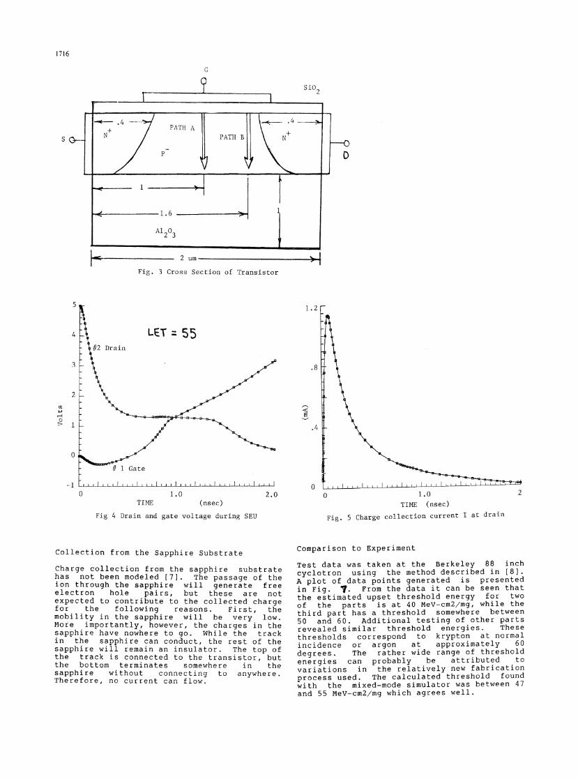
Fig. 3 shows a cross section of the finiteelement model used. Hits were simulated attwo positions A and B in the channel. Thephysical models used include bandgapnarrowing, concentration dependent ShockleyReed Hall recombination and Augerrecombination. The charge column simulatedhad a uniform generation rate along it'slength and a Gaussian distribution in theradial direction. The 1/e distance for theGaussian was .1 micron.
Transistor Q4 is the "struck" device. Acomposite model is used for Q4 consisting ofthe parallel connection of a standard SPICEtransistor and a finite element PISCES model.This was' done because the charge columnproduced by the SEU will only effect a portionof the channel of Q4. The rational forsplitting Q4 can be seen by again examiningFig. 1. (Note that the actual channel of Q4is 7 microns wide, while Fig. 1 is only 2microns wide). It can be seen that only theelectron contours in the vicinity of theparticle are distorted, while the contours atthe edges are unaffected. For this reason Q4was split into a 1 micron wide finite elementmodel and a W-1=6 micron wide SPICE model.
Plots of the voltage at nodes 1 and 2 aregiven in Fig. 4. In this simulation a LET of55 MeV-cm2/mg along path B was used. Node 2is the drain of Q4 and starts out at 5 volts.The voltage at 2 then falls, due to charge
Fig. lb Equipotential contoursTime = . 25pS
collection, to approximately 1.5 volts. Node1, the gate of Q4, starts at 0 (indicating Q4is off). Node 1 then dips below ground for aninstant due to capacitive coupling to node 2.Finally, the voltage at node 1 rises and nodes1 and 2 switch states indicating the cell hasupset.
Fig. Ic Electron contoursTime = . 25pS
Fig. 5 gives the charge collection current Iwhich flows into the finite element model.The total integrated charge under Fig. 5 is.44 pC which agrees with the critical chargefound during SPICE simulation alone. On theother hand the total charge deposited withinthe silicon layer by the ion was:
55 MeV-cm2/mg * .01 pC-mg/Mev-cm2-um * .4um= .220pC
The fact twice as much charge was collectedthan was deposited by the ion came as asurprise to us, but has been reported beforein connection with dose rate upset by Davis etal [5]. This "multiplication" of charge mayalso account for the discrepancy between theSPICE SEU critical charge (.3pC) and theexperimental SEU value (.188pC to .24pC)described in the above reference.
Fig. 6 shows the voltage at the drain andgate of Q4 with a hit of 47 MeV-cm2/mg alongpath B. In this case, the cell did not upsetand the drain and gate are returning to theiroriginal potentials at the end of thesimulation. The total charge collected was.37pC while the deposited charge was .J88pCgiving a charge "multiplication factor" of1.96. In this circuit, the relatively slowresponse time of the circuit in comparison tothe charge collection mechanism causes thecollected charge to linearly track the LET ofthe particle.
In faster circuits, if simulations areperformed just below and above the thresholdLET, more charge is be collected belowthreshold, when the circuit does not upsetthan above threshold, when it does. Thishappens because in faster circuits, thecircuit upsets and changes state before thecharge collection process is complete. (Oncethe circuit changes state and the voltage atthe drain drops, charge collection stops.)

1715
+5V
WZl
Fig. 2 Circuit Simulated
Additional Charge Collection Simulations:
In order to gain greater insight into thecharge collection process a number ofsimulations were conducted with the drainfixed at 5 volts, while the source and gateare held at ground potential. Simulationswere conducted at three substrate dopinglevels, two gate oxide thicknesses and variouscombinations of mobility (some unphysical).With substrate doping of 1.5e17, while only.16 pC was deposited in the device by the ion,.28 pC is collected at the drain. Thiscorresponds to a "charge multiplication"factor of 1.75. Using substrate doping oflel6, .32 pC (multiplication factor 2.0) wascollected.
One surprising result found during thesimulations was that the total collectedcharge did not depend strongly upon theposition of the charge track within thechannel. A 40 MeV-cm2/mg ion caused .26pC tobe collected at the drain at position A and.28pC at position B (see Fig. 3). Thecollection time and peak current were verydifferent in the two cases. At position A thepeak current was 7.8mA and the collection time(1/e) 50psec, while at position B the peakcurrent was .8mA and 500psec were needed.
The sensitivity of the multiplication factorobserved in the simulations to some processparameters is summarized in the followingtable. (Tox is the oxide thickness, Un theelectron mobility, Up the hole mobility, Nathe channel coping, L the channel length, andM the multiplication factor.)
Table 1
Tox Un Up Na
350 380 190 1.5e17350 380 190 1.0e16350 380 190 1.0e15
L
1. 1 51.151.15
1000 380 190 1.5e17 1.15350 380 190 1.5e17 1.5
350 1000350 100350 1000
5001000100
1 . Oe161 . Oe161 . Oe16
1.151.15
1.15
M
1.752.02.25
The multiplication factor shows a very strongdependence upon the ratio of electron-to-holemobilities. This behavior is reminiscent ofHu's charge collection model [6]. In Hu'smodel, the collected charge is proportional toa factor
1 + Un/Up
for diodes fabricated with N+ on a P-substrate.
Charge collection in these SOS devices can beviewed as being similar to charge transport ina bipolar transistor. The source acts as theemitter the drain as the collector and thelightly doped channel region as the base. Thecollection scenario can be described asfollows.
1. Holes generated by the ion in the P-typechannel region "short out" the space chargeregion at the drain and cause the electricfield which had been confined to the drain toexpand and fill the entire channel (see fig.1).
2. Electrons move to the right in response tothe electric field with velocity Un * E andare collected at the drain.
3. Holes move to the left with Up * E and arecollected at the source.
4. Theforwardchanneldrain.
PN junction at the source now becomesbiased and injects electrons into the
which replace those collected at the
5. The above process continues untilholes are removed from the baseequilibrium is restored.
alland
The total charge collected should then be:
Qcol = Qd * (1 + Un/Up)
as in Hu's model. Here, Qcol is the collectedcharge and Qd is the amount of chargedeposited by the ion in the drain space chargeregion. Due to the small size of the device,Qd can be replaced by the total chargedeposited by the ion since any chargedeposited in the channel by the ion willdiffuse into the drain depletion layer.
A study of Table 1, however, reveals that theprocess is more complex than this. Forexample, the relation of mobility to themultiplication factor does not follow a simplelinear relation as predicted above. Inaddition, the dependence upon channel dopingdoes not follow a square root relation as inHu's model. Finally, the dependence uponchannel length and oxide thickness defyexplanation by any simple model. The best wayto model charge collection in a device of thiscomplexity appears to be via numericalsimulation. Fortunately, the dependence ofcollected charge upon particle LET was foundto be linear (over one order of magnitude),which makes it easier to guess trial valuesfor the LET.
1.931.4
2.25.74
7.14
1716
G
S
Fig. 3 Cross Section of Transistor
5
4
3
2a
01- 1
LET= 55!#2 Drain
.8
.4
# 1 Gate
00 1.0 2.0 0 1.0
TIME (nsec)Fig 4 Drain and gate voltage during SEU
Collection from the Sapphire Substrate
Charge collection from the sapphire substratehas not been modeled [7]. The passage of theion through the sapphire will generate free
electron hole pairs, but these are not
expected to contribute to the collected chargefor the following reasons. First, themobility in the sapphire will be very low.More importantly, however, the charges in the
sapphire have nowhere to go. While the trackin the sapphire can conduct, the rest of thesapphire will remain an insulator. The top ofthe track is connected to the transistor, butthe bottom terminates somewhere in thesapphire without connecting to anywhere.Therefore, no current can flow.
TIME (nsec)
Fig. 5 Charge collection current I at drain
Comparison to Experiment
Test data was taken at the Berkeley 88 inchcyclotron using the method described in [8].A plot of data points generated is presentedin Fig. 7. From the data it can be seen thatthe estimated upset threshold energy for twoof the parts is at 40 MeV-cm2/mg, while thethird part has a threshold somewhere between50 and 60. Additional testing of other partsrevealed similar threshold energies. Thesethresholds correspond to krypton at normalincidence or argon at approximately 60degrees. The rather wide range of thresholdenergies can probably be attributed tovariations in the relatively;new fabricationprocess used. The calculated threshold foundwith the mixed-mode simulator was between 47and 55 MeV-cm2/mg which agrees well.
I1

1717
5
The sensitive area (from asymtotic crosssection) for all the parts was found to bebetween 5e-8 and 7E-8 cm2 per bit. Thiscorresponds almost perfectly to the channelarea (lum x 7um) of the single sensitiveN-channel transistor in each cell. In thiscircuit, P channel transistors were notsensitive to upset. There are two reasons forthis. First the critical charge (due to theW/L ratios of the P and N channel FETs) forthe P channel FET is much larger (.8pC vs.44pC). The second reason is the lowermobility of holes as compared to electrons.In P channel devices, the scenario describedabove remains the same; however Un and Up areinterchanged. Since Un is larger than Up, themultiplication factor will be smaller.
Conclusions
Mixed mode circuit-device simulations of SOSparts have been conducted and found to agreewell with cyclotron test data. During thesimulations charge multiplication throughibipolar action has been observed. Thisprocess results in collection of approximatelytwice as much charge at the drain as wasdeposited in the device by the ion. The exactmultiplication factor is dependent upon anumber of processing variables, includingchannel doping, channel length, and oxidethickness.
Acknowledgment:
As those readers familiar with cyclotrontesting will know, testing at the Berkeleycyclotron is no simple task. I would,therefore, like to thank the following peoplefor making the experiment possible. TheBerkeley 88-inch cyclotron staff for providinga beam; Jon Osborn and John Elder for testhardware and software design; John Nocerinofor design and fabrication of the test circuitboard; Rocky Koga for running the experimentwhen Al Kolasinski was gone; Bob Walter forsetting up the test chamber; Tim Morse and TomTsubota for testing the parts at 2 a. m. ;Managers Kevin Wilson and Murry Glick forencouragement and support; and, finally, RuthWilson for clerical support. This work was
funded by the Aerospace Sponsored Researchprogram of the Aerospace Corporation.
-4
-6
-8
al S/N #1
A S/N #2
0 S/N #3A
AL
No Errors S/N #3
Co
-1
02
TINE (nsec)Fig. 6 Drain and gate voltage (no upset)
References:
[1] M. R. Pinto, C. S. Rafferty, H. R.Yeager, R. W. Dutton, PISCES-IIb Users Guideand Supplementary Report, Stanford ElectronicsLaboratories, Stanford University, (1985)
[2] L. W. Nagel, SPICE2 Users Guide,Electronics Research Laboratory, University ofCalifornia Berkeley, (1975)
[3] J. S. Fu, H. T. Weaver, R. Koga, W.A. Kolasinski, "Comparison of 2D Memory SEUTransport Simulation with Experiments," IEEETrans. Nuc. Sci. NS-32, No. 6, pp4145-4150 (1985)
[4] J. G. Rollins, J. Choma, Jr."Mixed-Mode PISCES-SPICE Coupled Circuit andDevice Solver," submitted, IEEE Trans.Computer Aided Design
[5] G. E. Davis, L. R. Hite, T. G.Blake, C.-E. Chen, H. W. Lam, R. DeMoyer,Jr., "Transient Radiation Effects in SOIMemories," IEEE Trans Nuc. Sci. NS-32, No.6, pp 4432-4438, (1985)
[6] C. Hu, "Alpha-Particle-Induced FieldEnhanced Collection of Carriers," IEEE Elect.Dev. Let. EDL-3 31, (1982)
[7] A. B. Campbell, A. R. Knudson, W. J.Stapor, P. Shapiro, S. E. Diehl-Nagel, J.Hauser, "Charge Collection in CMOS-SOSStructures," IEEE Trans. Nuc. Sci. NS-32,No. 6, pp 4128-4133, (1985)
[8] R. Koga, W. A. Kolasinski, "Heavy-IonInduced Single Event Upsets of ModernMicrocircuits," IEEE Trans. Nuc. Sci.NS-31, No. 6, pp 1190-1196, (1984)
a
0 20 40 602LET MeV-cm /mg
Fig. 7 Experimental LET data
D 80
LET 414
3
2'-4
0
1
0
1-
N
E
0
0
1U _ _
V
.4 n