si and sige nanowire for micro-thermoelectric generator: a
TRANSCRIPT

REVIEWpublished: 26 March 2021
doi: 10.3389/fmats.2021.611078
Frontiers in Materials | www.frontiersin.org 1 March 2021 | Volume 8 | Article 611078
Edited by:
Emrah Celik,
University of Miami, United States
Reviewed by:
Mutabe Aljaghtham,
Prince Sattam Bin Abdulaziz
University, Saudi Arabia
Ovgu Ceyda Yelgel,
Recep Tayyip Erdogan
University, Turkey
*Correspondence:
Guilei Wang
Henry H. Radamson
Specialty section:
This article was submitted to
Energy Materials,
a section of the journal
Frontiers in Materials
Received: 28 September 2020
Accepted: 26 February 2021
Published: 26 March 2021
Citation:
Li Y, Wang G, Akbari-Saatlu M,
Procek M and Radamson HH (2021)
Si and SiGe Nanowire for
Micro-Thermoelectric Generator: A
Review of the Current State of the Art.
Front. Mater. 8:611078.
doi: 10.3389/fmats.2021.611078
Si and SiGe Nanowire forMicro-Thermoelectric Generator: AReview of the Current State of the ArtYou Li 1,2, Guilei Wang 1,2,3*, Mehdi Akbari-Saatlu 4, Marcin Procek 4 and
Henry H. Radamson 1,2,3,4*
1 Key Laboratory of Microelectronics Devices & Integrated Technology, Institute of Microelectronics, Chinese Academy of
Sciences, Beijing, China, 2Microelectronics Institute, University of Chinese Academy of Sciences, Beijing, China, 3 Research
and Development Center of Optoelectronic Hybrid IC, Guangdong Greater Bay Area Institute of Integrated Circuit and
System, Guangzhou, China, 4Department of Electronics Design, Mid Sweden University, Sundsvall, Sweden
In our environment, the large availability of wasted heat has motivated the search
for methods to harvest heat. As a reliable way to supply energy, SiGe has been
used for thermoelectric generators (TEGs) in space missions for decades. Recently,
micro-thermoelectric generators (µTEG) have been shown to be a promising way to
supply energy for the Internet of Things (IoT) by using daily waste heat. Combining
the predominant CMOS compatibility with high electric conductivity and low thermal
conductivity performance, Si nanowire and SiGe nanowire have been a candidate for
µTEG. This review gives a comprehensive introduction of the Si, SiGe nanowires, and
their possibility for µTEG. The basic thermoelectric principles, materials, structures,
fabrication, measurements, and applications are discussed in depth.
Keywords: Si, SiGe, nanowire, thermoelectric generator, ZT, heat
INTRODUCTION
Global warming has become a significant problem in today’s world, and environmental awarenessis stronger than it ever has been before (Moss et al., 2010). Researchers have long been focused onlocating new carbon-free and environmentally friendly energy alternatives (Radousky and Liang,2012). The waste heat from engines was considered to be a low-grade energy in the past centurybut is now seen as a fantastic energy source for the near future. Most of the energy that weconsume is wasted in the form of heat. Thermal energy scavenging or harvesting, achieved by athermoelectric generator (TEG), has the strength of stable components, high reliability, long servicelife, no maintenance, and direct energy conversion (Yan et al., 2018). Because of this, TEGs havebecome the most promising device with core materials for harvesting wasted heat, as a result of atemperature difference.
The first generation of TEGs was manufactured from semiconductors e.g., bismuth telluride(Bi2Te3), lead telluride (PbTe), and silicon germanium (SiGe). Except for Bi2Te3, those materialshave been used in deep-space missions, like NASA’s Voyager, Pioneer, Ulysses, and Cassinispace ships using radioisotope thermoelectric generators (RTGs) (June and Zakrajsek, 2017).Radioisotope thermoelectric generators can supply enough power for electronic devices in spaceprobes and satellites using the thermal energy from nuclear fission (Yang and Caillat, 2011). Some ofthose devices have operated formore than 30 years, showing their stability and reliability. One of themain drawbacks of TEG is the low efficiency compared with other types of power generators. Thislow efficiency problem has made it difficult to use TEGs for an ecological niche in the past decades.

Li et al. Si/SiGe Nanowire µTEG
In recent years, different research groups have fabricatedmicro-thermoelectric generators (µTEGs) which are muchsmaller than the traditional TEGs (Gadea et al., 2018b; Noyanaet al., 2019). Micro-thermoelectric generators fabrication applythe NW techniques commonly used in CMOS technology ormicroelectromechanical systems (MEMS) (Radamson et al.,2017, 2019).
This also reduces the cost by using micro-patterning whichcan be integrated with other microfabricated devices (Gadeaet al., 2018a). Over the past decades, figure-of-merit (ZT) wasincreased slowly with existing materials and structures, with therealized value in the vicinity of 1, thus little attention has beenpaid to the thermoelectric (TE) field. Though slowly, the TEindustry has developed steadily by finding its niches for spaceexploration and laboratory and medical applications, where theavailability and reliability of energy is more overwhelming thanthe cost and efficiency (Radamson et al., 2019).
Recently, scientists have experimented with manynanostructured materials to make a high performance µTEG.Besides the elementary substances like bismuth (Kim et al.,2015) and silicon (Li et al., 2003b), a large number of compositematerials, including clathrates (Kleinke, 2010; Takabatake et al.,2014), skutterudites (Nolas et al., 1999; Rogl et al., 2014), metaloxides (Koumoto et al., 2010; Ishibe et al., 2018), tellurides(Heremans et al., 2008; Poudel et al., 2008; Goldsmid, 2014),and intermetallics (Zeier et al., 2016), have been investigated fortheir TE performance. A key issue for this TE research is to finda high-performance TE material with low thermal conductivityand high electric conductivity. More possible solutions havebeen put forward and verified; one of the most promisingmaterials is silicon. Silicon and its Group IV binary or ternaryalloys have potential to be used to form a TEG in commercialapplication for several reasons. They would be Si-based CMOStechnology compatible, the source of the Group IV materialsis much cheaper than the traditional TE materials, and ratherthan poisonous materials like Bi2Te3, the Group IV materials areenvironment-friendly and safe for civil use.
However, despite its high thermal conductivity, Si bulk isunideal for TEG. Because of the popularization of Si electronics,research on Si TE devices are expanding (Ni et al., 1995).Two promising roads have been researched to improve theTE performance. The former is the alloying effect, whichintroduces other extended group IV materials with the samelattice structure, the typical one being SiGe. Compared to pristineSi, the experiment results show a distinct decrease in thermalconductivity. Interest has also been given to nanostructures,with quantum confinement applied. The development innanoengineering makes it possible for nanostructures in Si-basedTEG. The low-dimensional structures exhibit a significantlyreduced lattice thermal conductivity compared to their bulkcounterparts owing to the enhanced phonon scattering at theinterfaces, and nanowires (NWs) have been proven with high ZT(Dresselhaus et al., 2007).
The two methods could be combined fabricate TEG with Siand SiGe NWs. Specifically, the Si and SiGe NWs have exhibitedhigher TE performances related to their bulk crystal counterpartsboth in experimental and theoretical studies since the early
1990s (Li et al., 2003a,b; Hochbaum et al., 2008). Differentexplorations of the elements that affect TE have been put forwardby several groups like alloy, surface roughness, doping, etc.,Silicon (Si) NWs exhibited a ZT of 0.6 at 300K (∼0.01 for bulkSi) without degeneration of the Seebeck coefficient and electricalconductivity (Hochbaum et al., 2008). Moreover, the thermalconductivity is further reduced in SiGe NWs (Li et al., 2003a).The longer SiGe NW arrays gives a higher Seebeck coefficient andthe thermal conductivity decreases with increasing Ge contentand NW length (Li et al., 2012).
Nowadays, with further research, Si-based CMOS technologyshows its potential to make a high-performance µTEG (Gadeaet al., 2018b). Meanwhile, the scaling down in the fabricationof CMOS makes it possible to grow extremely thin Si and SiGeNWs. In general, two approaches have been adopted for thefabrication of different NWs: top-down or bottom-up (Akbari-Saatlu et al., 2020). In most of the research we have investigated,the bottom-up approach is preferred with the popular vapor-liquid-solid chemical vapor deposition (VLS-CVD) used (Calazaet al., 2015); others are achieved using the top-down approachwith an etching process, for example, metal-assisted wet chemicaletching (MaCE) or reactive ion etching (RIE) (Wolfsteller et al.,2010; Sandu et al., 2019; Radamson et al., 2020). Some relevantmeasurements of the TE properties have also been developedduring the study of NWs (Rojo et al., 2013; Borup et al., 2015;Liu et al., 2016). The typical methods for the Seebeck coefficientmeasure are mesoscopic or microfabricated suspended devicesand thermocouples. The microfabricated suspended devices havealso been used in the measurement of thermal conductivity. Theother methods commonly used are the 3ωmethods and scanningthermal microscope (SThM) technique (Grauby et al., 2013).Micro-thermoelectric generators has a great variety of potentialapplications, including business electronics, bio-medical devices,and internet of things (IoT) devices. Internet of things devices arethe most promising prospect for the µTEG with a steady µW-mW level energy supply (Haras and Skotnicki, 2018; Zhang et al.,2018).
In this review article, we examine the past and existingresearch into TEG and µTEG, especially based on the Si andSiGe NWs. The basic TE principles and theories are introducedand the factors that may influence the TE performance of Siand SiGe NWs are discussed. The superiority of the group IVmaterial-based NWs as TE materials are detailed with feasiblestructures while their fabrication methods and TE measurementsare also reviewed. Finally, the existing Si and SiGe NW µTEGsare discussed for their potential applications and the feasibleapplications are illustrated.
THEORY AND PRINCIPLE
Based on the three fundamental TE principles, the Seebeck effect,the Peltier effect, and the Thomson effect, TE devices such asTEGs and TE coolers have been fabricated (Figure 1). To detailthe mechanisms in TEGs fabricated using materials like Si andother group IV NWs, researchers have proposed some theoriesbased on the semiconductor physics model to explain it.
Frontiers in Materials | www.frontiersin.org 2 March 2021 | Volume 8 | Article 611078

Li et al. Si/SiGe Nanowire µTEG
FIGURE 1 | Sketch of thermoelectric device: (A) Thermoelectric generator; (B) Thermoelectric cooler. Reprint with permission from Pennelli (2014). Copyright 2014
Journal of Nanotechnology.
ZT and Energy Conversion EfficiencyTo measure the TE energy conversion efficiency of TEG,researchers adopted the parameter called dimensionless figure ofmerit, denoted as ZT, which is defined as (Rowe, 1995):
ZT =σS2
κT
where S is the Seebeck coefficient, σ the electrical conductivity,T the operating temperature, and κ the thermal conductivity.In some cases, when κ is unavailable for ZT calculation, theparameter which is defined as TE power factor:
PF = σS2
can be an indicator (Rowe, 1995). To improve the TE propertyof TEG, two approaches have been considered: (1) improve thepower factor S2σ , (2) decrease the thermal conductivity κ . Sinceelectron scattering in a semiconductor is negligible, interest hasbeen focusing on the method to lower the thermal conductivity.
For the conventional TEG, ZT is defined as (Rowe, 1995):
ZT =(Sp − Sn)
2· T
(√
κpσp
+
√
κnσn
)2
where the subscripts p and n denote the P-type and N-typelegs, respectively.
The maximum conversion efficiency is defined by (Rowe,1995):
ηmax = η0 ·
√
1+ ZTavg − 1√
1+ ZTavg +TcTh
where η0 = (Th –Tc)/Th is the Carnot ideal cycle efficiency. Here,the Th is the hot junction temperature, Tc for the cold side. ZTavg
is the average value of ZT from Tc to Th. The certain relations
between Th, ZTavg , and η are shown in Figure 2 (Yu et al.,2019). Like other types of heat power generation, η increaseswith temperature difference and is confined to the Carnot limit(Gadea et al., 2018a). Conversion efficiency of different typesof energy sources for electric generations like geothermal, solar,nuclear, and coal are also presented in Figure 2, which can bea comparation.
The highest ZT has achieved more than 2 for some materials(Kumar et al., 2020), and there are some calculations andmodels which speculated that there is still potential for ZT.But it is noteworthy that for different temperatures, the ZTvaries widely; the most valuable temperature is 300K, which isthe device’s normal operate temperature. For Si, ZT = 0.2 isachieved at 620K with the optimized contact in a recent work(Gadea Díez et al., 2020).
Thermal ConductivityFourier’s law is defined as: j= –κ∇T, where thermal conductivityκ is the ratio of heat flux j that passes through unit area per unittime to temperature gradient ∇T (Swinkels and Zardo, 2018).In a semiconductor, κ = κph + κe is the sum of two mainparts, dominating phonon thermal conductivity and negligibleelectron thermal conductivity κe. Phonon thermal conductivityκph = LphvsCv/3 is related to heating transport through phonons,depending on the phonon’s mean free path of certain materials(MFP, Lph = v
sτ is the phonon mean free path, with τ phonon
lifetime), sound velocity (vs), and heat capacity (Cv). Electronthermal conductivity is calculated by the Wiedemann-Franz lawκe = L0σT where L0 ≈ 2.45 × 10⁻⁸ V2 K−2 is theLorentzconstant for degenerately doped silicon (Minnich et al., 2009),representing heat propagation with charged carriers, σ theelectrical conductivity, and T the average temperature betweenthe cold and hot side. Molecular dynamics (MD) and firstprinciple calculation techniques have been used in several studiesto calculate the theoretical value of the thermal conductivity of Si
Frontiers in Materials | www.frontiersin.org 3 March 2021 | Volume 8 | Article 611078

Li et al. Si/SiGe Nanowire µTEG
FIGURE 2 | TE energy conversion efficiency (η) vs. hot-side temperature (Th) for different ZTavg values. Reprint with permission from Yu et al. (2019).
and SiGe (Chen et al., 2009; Garg et al., 2011; Yang and Minnich,2017).
Phonon Thermal ConductivityThermal conductivity is actually related to the lattice thermalconductivity, and it consists of different kinds of phononscattering. This is caused by defects or dopants with disorganizedlattice periodicity; the scatterings reduce the MFP to a largeextent. Other particles and quasiparticles, like electrons, can alsoproduce scattering using the energy and momentum exchange.These scattering mechanisms have been formulated by theMatthiessen’s rule (Gadea et al., 2018a):
1
τp,i=
1
τpN,i+
1
τpR,i
1
τpR,i=
1
τpU,i+
1
τpA,i+
1
τpB,i+
1
τpC,i+
1
τpE,i
In the above formula, the phonon relaxation time is comprised ofmultiple phonons scattering events including phonon–phononnormal scattering, phonon–phonon Umklapp scattering,phonon alloy scattering, phonon boundary scattering, phononcluster scattering, and phonon electron scattering (Yi and Yu,2015).
Mainly, researchers focused on the most important partslike phonon-boundary scattering and phonon alloy scattering.Although phonon boundary scattering is frequency independent,it is mainly influenced by the low frequency phonons with longwavelength (Kim, 2013). Phonon boundary scattering is causedby the grain boundary and it is dominant where the dimension ofthe structure is much smaller than the phonon MFP. Therefore,the phonon thermal conductivity is strongly depressed and theheat flux through the system is limited by the thermal boundary
Kapitza resistance (Cahill et al., 2003). For silicon NW, itsphonon mean free path is ∼300 nm while its electron mean freepath is ∼110 nm with heavy doping (Ju and Goodson, 1999).Considering this, the diameter of a Si NW should be thinner than300 nm but more than 110 nm. Then the κ will be reduced forthat κph = LphvsCv/3, so the thermal conductivity of a single SiNW decreases when the diameter decreases.
When we discuss the influence of phonon boundary scatteringon the κ , the surface roughness of the NWs is an important issue.Thermal conductivity reduction caused by surface roughness hasbeen observed in several experimental works (Hochbaum et al.,2008; Kim et al., 2011; Feser et al., 2012; Malhotra and Maldovan,2016); κ was reported with a value down to few W m−1 K−1 inNWs with a diameter of several tens of nms, much lower thanthe bulk Si (∼150W m−1 K−1). By theoretical prediction, the κ
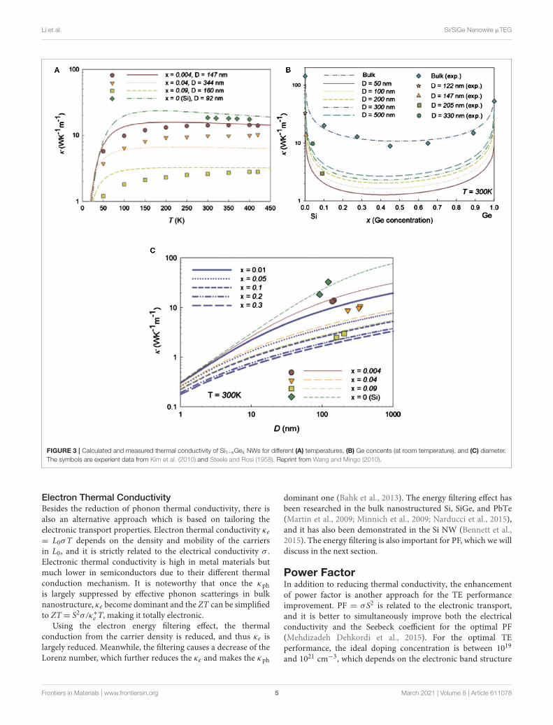
in Si NWs with a diameter <100 nm was proportional to (D/1)2,where D was diameter and 1 the surface roughness. An analysisshows that the experimental data fits well with the calculationdata, indicating the dependence between D and κ (Figure 3).
Other mechanisms, like point defect scattering in Si1−xGexalloy, also result in the reduction of λph. Figure 3 shows the κ
behavior of Si1−xGex NWswith Ge concentration x= 0.004, 0.04,and 0.09. The figure reveals that the alloy scattering is aggravatedby the increased Ge content. At the same Ge concentration, thethermal conductivity is decreased with a smaller diameter, whichhas been confirmed in previous research (Li et al., 2003b). Inprinciple, alloy scattering causes a severe suppression of high-frequency phonons in Si1−xGex, thus the low frequency phononsbecame the dominant ones (Xie et al., 2014). Meanwhile,compared with Si NWs, a stronger length dependence, weakerdiameter, and surface roughness dependence have been shownto occur in Si1−xGex NWs thermal conductivity (Xie et al.,2014).
Frontiers in Materials | www.frontiersin.org 4 March 2021 | Volume 8 | Article 611078
Li et al. Si/SiGe Nanowire µTEG
FIGURE 3 | Calculated and measured thermal conductivity of Si1−xGex NWs for different (A) temperatures, (B) Ge concents (at room temperature), and (C) diameter.
The symbols are experient data from Kim et al. (2010) and Steele and Rosi (1958). Reprint from Wang and Mingo (2010).
Electron Thermal ConductivityBesides the reduction of phonon thermal conductivity, there isalso an alternative approach which is based on tailoring theelectronic transport properties. Electron thermal conductivity κe= L0σT depends on the density and mobility of the carriersin L0, and it is strictly related to the electrical conductivity σ .Electronic thermal conductivity is high in metal materials butmuch lower in semiconductors due to their different thermalconduction mechanism. It is noteworthy that once the κphis largely suppressed by effective phonon scatterings in bulknanostructure, κe become dominant and the ZT can be simplifiedto ZT= S2σ /κ∗
e T, making it totally electronic.Using the electron energy filtering effect, the thermal
conduction from the carrier density is reduced, and thus κe islargely reduced. Meanwhile, the filtering causes a decrease of theLorenz number, which further reduces the κe and makes the κph
dominant one (Bahk et al., 2013). The energy filtering effect hasbeen researched in the bulk nanostructured Si, SiGe, and PbTe(Martin et al., 2009; Minnich et al., 2009; Narducci et al., 2015),and it has also been demonstrated in the Si NW (Bennett et al.,2015). The energy filtering is also important for PF, which we willdiscuss in the next section.
Power FactorIn addition to reducing thermal conductivity, the enhancementof power factor is another approach for the TE performanceimprovement. PF = σS2 is related to the electronic transport,and it is better to simultaneously improve both the electricalconductivity and the Seebeck coefficient for the optimal PF(Mehdizadeh Dehkordi et al., 2015). For the optimal TEperformance, the ideal doping concentration is between 1019
and 1021 cm−3, which depends on the electronic band structure
Frontiers in Materials | www.frontiersin.org 5 March 2021 | Volume 8 | Article 611078

Li et al. Si/SiGe Nanowire µTEG
of materials (Tritt, 2011; Schierning, 2014). The relationsbetween the TE parameters and doping concentration forthe alloy Si80Ge20 are shown in Figure 4; κ , σ , S, and ZTvary with the doping concentration in different tendency(Minnich et al., 2009).
A simulation has studied the optimal power factor in Si NWwith different sizes, and the relation of S, σ , and PF vs. the cross-section area (area) and carrier concentration (n) are shown inFigure 5 (Shi et al., 2009). The thinner Si NW will have largerS and smaller σ , and thus slightly increase the PF, and propercarrier concentration is needed for the optimal PF.
The research studies about the TE power factor enhancementare based on the nanostructures of different materials to a greatextent (Mehdizadeh Dehkordi et al., 2015); here we only give abrief introduction of the mechanism of electrical conductivityand Seebeck coefficient.
Electrical ConductivityThe electrical conductivity is always an important parameter forelectronic devices as well as for TE ones. This parameter is mainlydependent on Kelvin temperature and the electronic relaxationtime in a material. In principle, the carriers can interact withdifferent scattering centers e.g., impurities or phonons, and therelaxation time may be affected. More specifically, the scatteringcenters are categorized by ionized and neutral impurities (Iand N) and deformation potential (D) created by phonons.These scatterings mostly occur simultaneously, therefore, thetotal relaxation time is written by Matthiessen’s rule (Yi and Yu,2015).
1
τe=
1
τD+
1
τI+
1
τN
The deformation potential is governed by electronic carriersscattering through the acoustic vibration of atoms in the crystallattice and intervalley scattering caused by optical phonons(Yi and Yu, 2015). The modulation-doping is remarkable forthe ionized impurity scattering which is dominant at a lowtemperature (Mehdizadeh Dehkordi et al., 2015).
Seebeck CoefficientBased on the Seebeck effect (Figure 1A) found in 1821, Seebeckvoltage V is proportional to the temperature difference 1T andSeebeck coefficient S (also thermopower) (Gadea et al., 2018a):
S =V
T
The Seebeck coefficient for semiconductors is typically on theorder of 100 µV/K (Goktas et al., 2018). Conversely, this processcan operate in reverse to make TE cooler (the Peltier effect,Figure 1B). In P-type semiconductors, S is a positive value(negative in N-type semiconductor). In the fabrication of aTEG, both N-type and P-type are applied to achieve a largerpotential difference.
For metals and degenerate semiconductors, the Seebeckcoefficient is defined as (Snyder and Toberer, 2008),
S =8π2kB
2
3eh2m∗T(
π
3n)23
where n is the charge carrier concentration, m∗ is the effectivemass of the charge carrier, h is the Planck’s constant, kB is theBoltzmann constant, and e is the carrier charge. S is stronglyinfluenced by the charge carrier energy distribution, and inparticular it increases when the average difference between thecarrier energies and the Fermi energy increases (Pennelli, 2014).
Dopants, defects, and interfaces can act as energy barriers.The caused energy filtering effect will suppress the low energyelectrons in the transport, and thus increase the S and PFin a semiconductor (Schierning, 2014). Hicks and Dresselhaus(1993a) have presented a study about the effect of electronquantum confinement on TE properties of NWs. The resultsshow that interfaces cause energy barriers as energy filteringfor low energy electrons which are not active in the transport,resulting in an enhancement of PF (Martin et al., 2009). Theenhancement of PF in combination with the reduction of theκ are the two benefits for quantum dot and quantum wellstructures where density of electronic states is modified andphonon modes are frozen. The TE properties of quantum dotsand quantum wells are both theoretically foreseen (Hicks andDresselhaus, 1993b) and experimentally demonstrated (Harmanet al., 2002).
The longer SiGe NW arrays provide higher S and then κ isdecreased by increasing Ge content and NW length (Li et al.,2012). A TEG with short planar Si NWs have demonstrateda dramatic enhancement in the TE power density, attributingto the increase in S (Tomita et al., 2018a). This was explainedby the enhanced phonon drag effect, since the frequent surfacescattering in longer Si NWs will weaken this effect (Figure 6).
ADVANCED GROUP IV MATERIALS
Since the electric conductivity of a TEG was decreased as a resultof pursuing the high thermal conductivity, the better choice isan ideal material which integrates the opposite properties oflow thermal conductivity and high electric conductivity (σ ),with an as high as possible Seebeck coefficient (S). Therefore,the concept called phonon glass-electron crystal (PGEC) hasbeen put forward which involves limiting the minimum electronscattering (small electron mean free path), like the crystallinematerial, and high phonons scattering (large phonon mean freepath), like the amorphous material.
Bismuth telluride (Bi2Te3) and its (Bi1−xSbx)2(Se1−yTey)3alloy family are the most used TE materials because of their highTE conversion efficiency at room temperature. Also, their easydeposition in thin filmmakes the module flexible (Siddique et al.,2017). However, the process price of these traditional foundationmaterials is also an important issue. A review of the materialprice of the TE is listed as: Lead (Pb ∼2.50$/kg), Bismuth (Bi∼10.5$/kg), Antimony (Sb ∼9$/kg), Selenium (Se ∼24$/kg),or Tellurium (Te ∼36$/kg) (Haras and Skotnicki, 2018). Asa comparison, the pristine silicon is much cheaper as a TEmaterial due to the increase in photovoltaic power generation (Si∼1.5$/kg). Silicon also has the advantage of being low cost withthe CMOS-compatible processing. Furthermore, when countingother recessive and dominant costs, like environment friendliness
Frontiers in Materials | www.frontiersin.org 6 March 2021 | Volume 8 | Article 611078

Li et al. Si/SiGe Nanowire µTEG
FIGURE 4 | Normalized TE properies and ZT vs. doping concentration at
300K for N-type Si80Ge20 (Minnich et al., 2009).
and human innocuous, there is no doubt that silicon has anoverwhelming preponderance.
Si NWsWith the diamond structure (Fd-3m), silicon conducts heatlargely by phonon rather than the charge carrier (electron orhole). At 300K, thermal conductivity of pure silicon is ∼150Wm−1 K−1 (Glassbrenner and Slack, 1964). With doping, thethermal conductivity can be further reduced due to phononimpurity scattering (Slack, 1964). Silicon NW has shown itspriority in TE application. Compared with bulk Si, an extremereduction of thermal conductivity (1.6W m−1 K−1) has beendemonstrated for Si NWs with a 50 nm diameter without thedetriment of Seebeck coefficient and electrical resistivity values(Hochbaum et al., 2008). The strong diameter dependence ofSi NWs thermal conductivity has been demonstrated, whichis attributed to the enhanced phonon-boundary scattering andphonon spectrum modulation (Li et al., 2003b). The similarreduction of thermal conductivity from bulk to NWs has alsobeen reported inGe-based TE research. A sub-30 nmdiameter GeNWs was measured with a thermal conductivity of ∼1.5–2.3Wm−1 K−1 at 300K (Wingert et al., 2011), dramatically decreasedfrom Ge bulk (∼56Wm−1 K−1) (Glassbrenner and Slack, 1964).Also, we can see a decrease of thermal conductivity compared tothe Si NWs mentioned above, and the difference is explained bythe heavier atomic mass and decreased phonon velocities of Gewith respect to Si (Wingert et al., 2011).
Si NW arrays, which are largely parallel Si NWs, have beenfabricated on Si substrate with metal-assisted chemical etching(MaCE) in order to make a TEG.With an amount larger than 107
in several mm2, a 0.5mm thick sample chip, and NWs diameterbetween 60 and 120 nm, the thermal conductivity was measuredat∼ 4.6W m−1 K−1 (Pennelli et al., 2018).
Isotope doping can be a feasible way to reduce thermalconductivity. Isotope effect on the thermal conductivity of Si
NWs has been researched theoretically based on the non-equilibrium molecular dynamics (NEMD) method (Yang et al.,2008). Random isotope doping Si NWs and isotopic-superlatticeSi NWs are built in this research, the minimum thermalconductivity is 0.4W m−1 K−1 is shown in 28Si420.5Si0.5 NWswith cross sections of 1.6 × 1.6 nm2. Furthermore, a curve ofthermal conductivity vs. the concentration of doping isotopeatom (x) is exhibited, which shows a similar tendency withSixGe1−x and a plateau at 0.2 <x<0.8 (We will discuss thistendency in the next section). More simulations have beenconducted for the isotope effect on thermal conductivity, like theisotopic core-shell Si NWs (Hattori and Uno, 2013) and isotoperadial distribution (Royo and Rurali, 2016). The fabrication of Siisotope NWs is demonstrated in Mukherjee et al. (2015) usingthe VLS method and a 30% decrease of thermal conductivityis shown in isotopically mixed 28Si30x Si1−x NWs comparedwith isotopically pure 29Si. This is in agreement with theaforementioned simulation.
Si1−xGex Alloy NWsStarting in the 1970s, SiGe alloys have been applied in RTGsfor the power systems in NASA space missions (with ZT ∼0.5for P-type and ∼0.9 for N-type at 1,073K; Rowe, 1995). Laterimprovements were realized in nanostructured bulk SiGe withZT ∼1.3 at 1,173K for N-type (Wang et al., 2008a) and ZT∼0.95 at 1,073K for P-type (Joshi et al., 2008). A recent studyhas fabricated Si80Ge20B0.5 bulk alloy with the maximum ZT of0.71 at 1,073K using melt spinning (MS) combined with sparkplasma sintering (SPS) (Wongprakarn et al., 2018).
Like Si NWs, SiGe alloy NWs exhibited excellentenhancement as a result of the phonon boundary scattering.Individual P-type SiGe alloy NW was reported with thermalconductivity ∼1.1W m−1 K−1 and ZT ∼0.18 at 300Kexperimentally (Martinez et al., 2011). In a typical TE modelingof SiGe NWs, the optimized ZT is 1.3 at 800K for theSi0.73Ge0.27 NW with 26 nm diameter where the ionizedimpurity concentration should be about 1.0× 1020 cm−3 (Yi andYu, 2015). In principle, the ZT of SiGe at different temperaturescan be further enhanced by the diameter reduction and dopingconcentration optimization. The reduction in SiGe alloy NWscame from the phonon alloy scattering which scatters shortwavelength phonons with high frequency, while low frequencyphonons are scattered by the phonon boundary scattering (Liet al., 2003a).
Several studies have investigated the effect of Ge fraction(x) on the thermal conductivity (κ) in Si1−xGex NWs boththeoretically and experimentally (Wang and Mingo, 2010; Liet al., 2012; Yi and Yu, 2015). In an MD simulation, with x= 0.05, the κ of SiGe NW was decreased to half of that ofthe intrinsic Si NW, and the minimum thermal conductivitywas shown at x = 0.5, which is reduced to only 18% (Chenet al., 2009). With a similar tendency found in bulk SiGealloy, it has been shown that a dramatic reduction of thermalconductivity happens when the Ge concentration increases ina small scale less than x = 0.005 (Wang and Mingo, 2010).The further increasing of Ge content will decrease the thermalconductivity to approach the lower limit which is achieved at
Frontiers in Materials | www.frontiersin.org 7 March 2021 | Volume 8 | Article 611078

Li et al. Si/SiGe Nanowire µTEG
FIGURE 5 | (A–D) S, σ vs. area, n; (E–G) PF (P), optimal PF (Pmax), optimal carrier concentration (Nmax) vs. area, n. Reprint from Shi et al. (2009).
x ≈ 0.4. In fact, with x = 0.2, the thermal conductivity hasapproached the minimum and then a broad plateau exists inthe range of 0.2 <x<0.8 (Figure 3B). Such a plateau is causedby the phonon alloy scattering due to the large atomic massdifference between Si and Ge (Khatami and Aksamija, 2016).Then, the excessive Ge content makes the thermal conductivitydramatically reversing increase, and the κmin of NWs is muchsmaller than the bulk one.
A study on the surface doping effect shows different typesof alloying of SiGe, and Ge are used in a small fraction as adopant on the surface of Si NWs with a facile fabrication (Panet al., 2015). Compared to pristine Si NW, the Ge-coated Sivertical NW arrays show a 23% reduction in thermal conductivityat 300K, and such a decrease can be enhanced to 44% byannealing. Analyzed by X-ray photoelectron spectroscopy (XPS),the interaction between Ge surface doping and Si NWs is
Frontiers in Materials | www.frontiersin.org 8 March 2021 | Volume 8 | Article 611078

Li et al. Si/SiGe Nanowire µTEG
FIGURE 6 | Schematic of the thermal carrier behavior in the (A) long Si-NWs and (B) short Si-NWs. Reprint with permission from Tomita et al. (2018a).
enhanced by the binding energy shifting of Si-2p and Ge-3dafter annealing treatment. Moreover, simulated results by MDmethod shows the SiGe composition has to be graded in orderto effectively optimize the thermal conductivity. Compared tothe SiGe with abrupt interfaces, a 57% reduction of thermalconductivity was reported for the graded SiGe NW (Zhang et al.,2017).
Besides Ge fraction, diameter (D), and length of SiGe NWs arealso important issues for the TE properties (Li et al., 2003b;Wangand Mingo, 2010). The thin NWs show a reduction of thermalconductivity when compared with the thick ones. A thoroughstudy has been designed to find the certain trend (Shi et al., 2009),and the result is that thermal conductivity is proportional to Dwhen D is small. However, this dependence becomes continuallyweaker with increasing D. Combined with the Ge constituenteffect, the group found the linear trend slowed down with ahigher Ge content, up to x = 0.5. The same situation happenswith the increasing Si in Ge. This is because of the coexistenceof alloy and boundary scattering. SiGe NW arrays with a longerlength exhibit a higher Seebeck coefficient while the thermalconductivity decreases with increasing Ge concentration andNW length (Li et al., 2012).
When it comes to doping type, N-type SiGe NWs are reportedto have remarkably higher ZT and power factor compared toP-type SiGe NWs at 300K (Shi et al., 2010). With a crosssection area of 2.3 nm2, the ZT of N-type Si1−xGex NWs wastheoretically calculated to be ∼4.3 (Shi et al., 2010). In Norooziet al. (2017a), the peak of Seebeck coefficient for N-type andP-type Si0.53Ge0.47 are 8 and 1.8 mV/K at 315K, which canbe explained by the temperature dependence of the interactionof defects. With the same diffusion process applied, the carriermobility in N-type SiGe NWs is higher than P-type, which resultsin a much higher Seebeck coefficient in N-type SiGe NWs thanP-type. Also, the measured maximum power factor of N-type istwo times higher than P-type.
Other Promising Group IV MaterialsWith the prosperity of silicon-based technology, other GroupIV materials have also been studied as composite materials.They have similar crystal textures, so they have lower processingcosts and high compatibility. With the publications of theoreticaland experimental research, it was discovered that carbides andtin compounds with silicon and germanium have excellentTE properties.
SiCAs the recognized third generation semiconductor material,SiC has become a promising material for power electronics.Different advanced growth methods have been applied toimprove the crystal quality (Pécz et al., 1999; Yakimova et al.,2011). SiC has also been applied to other semiconductor devicesincluding composites, field emitters, supercapacitors, field-effect transistors, nanoelectromechanical devices, photocatalysts,sensors, microwave absorbers, and super-hydrophobic coating(Zekentes and Rogdakis, 2011; Wu et al., 2015; Chen et al., 2019).A lot of studies have presented the performances of SiC. Underthose investigations, SiC exhibits excellentmechanical properties,exceptional chemical stability, high power, high frequency,thermal stability, and low thermal conductivity (Zekentes andRogdakis, 2011; Wu et al., 2015; Chen et al., 2019). Some peoplehave investigated its TE properties to seek for the possibilityof SiC as a TE material (Choi et al., 2011). The revealedcharacteristics demonstrated the possibility for SiC as a superbTEG material which can work in harsh ambiences like high-power/high-temperature/high-voltage.
Both theoretical and experimental studies have been carriedout for the thermal properties of SiC NWs. NEMD simulationswere used on the lattice thermal conductivity of bulk β-SiC and NWs (Papanikolaou, 2008). Like Si and SiGe, adramatically reduced thermal conductivity has been shownin SiC NWs compared to the bulk SiC, similarly owing tothe boundary scattering and size confinement of phonons innanostructures. In another piece of research based on NEMD,the thermal conductivity of SiC NWs with modulated diametersand polytypes were predicted, and it was also found that theincrease of both the diameter and length can enhance the thermalconductivity of SiC NWs with the similar tendency of Si NWs(Termentzidis et al., 2013). A repeatable method involved placingthe individual or double β-SiC NWs on pre-patterned electrodesvia a nanomanipulator combined with focused ion beam (Leeet al., 2010), and the 3ωmethodmeasured thermal conductivitiesof the individual and double NWs were, respectively, 82 ± 6 and73± 5Wm−1 K−1. Likewise, the thermal conductivity, electricalconductivity, and Seebeck coefficient of SiC NWs were reportedas a function of temperature for the SiC NWs from 190 to 370K(Valentín et al., 2013). The Seebeck coefficient was measuredvarying from−17 to−68 µV/K with the temperature range, andat 300K the S varied from −22 to −56 µV/K, for N-type dopedSiC (Valentín et al., 2013). A simulation study demonstratesthat the thermal conductivity ranged from 4 to 12W m−1
Frontiers in Materials | www.frontiersin.org 9 March 2021 | Volume 8 | Article 611078

Li et al. Si/SiGe Nanowire µTEG
K−1, near 5W m−1 K−1 for ∼ 4 nm diameter. Similarly, thereduced diameter also decreased the thermal conductivity ofSiC NWs by comparing the three samples with different sizes.However, compared with the electric property searching of SiCfor microelectronic devices, the experiments for the TEG are stillinsufficient, thus more research should be carried out in this field.
Si-Ge-Sn Binary and Ternary AlloysCompared to C, Si, and Ge, Sn has a larger atomic mass andbigger atom diameter. The size difference has a large impact onTE performance. A variety of studies have demonstrated theiralloy effects significantly decrease thermal conductivity.
Theoretically, a group investigated the Sn alloying effect toSiGe on the thermal conductivity (κ) of SiGeSn alloys usingNEMD simulations with optimized Stillinger–Weber parameters(Lee and Hwang, 2017). The afore-mentioned broad plateauin SiGe alloy also appeared in the ternary alloys. With arealizable content range in 0 ≤ x ≤ 0.2, the κ of Si0.2−xGe0.8Snxalloy was much lower than the SiGe and GeSn alloys. Thepredicted minimum of κ occurred at x = 0.1 with a ∼40%reduction compared to those of Si0.2Ge0.8 and Ge0.8Sn0.2. Thisreduction is produced by the increased mass disorder scatteringof phonons similar to SiGe. Another theoretical study withphonon Boltzmann transport formalisms have simulated thephonon thermal conductivity of SiSn, GeSn, and SiGe-Sn alloysand their corresponding thin films (Khatami and Aksamija,2016). They showed that the minimum thermal conductivity ofSi1−xSnx alloys was 3W m−1 K−1 with x = 0.5 and 5.86W m−1
K−1 for the Ge1−ySny with y = 0.61, which can be the lowest ofthe three alloys, twice as low as SiGe. In contrast, their simulationof the 20 nm SiGe, SiSn, and GeSn thin films offer a furtherdecrease in κ with a value of 1.71Wm−1 K−1 for the Si0.51Ge0.49,0.91W m−1 K−1 for the Si0.41Sn0.59, 1.53W m−1 K−1 for theGe0.45Sn0.55, and 1.11W m−1 K−1 for Si0.36Ge0.32Sn0.32 whichare near the conductivity of amorphous SiO2 (Khatami andAksamija, 2016). Both pieces of research theoretically show theTE potential of Sn incorporated with SiGe.
Experimentally, phosphorous-doped Ge0.971Sn0.029 NWs isfabricated using RPCVD and its electrical conductivity andSeebeck coefficient data is compared to the Si and Ge NWs at250K for NWs with cross-sectional area of 700 × 50 nm andlength 22µm. The GeSn is measured with electrical conductivity∼550 �−1 cm−1, which is much larger than Si (231 �−1 cm−1)but less than Ge (653 �−1 cm−1), and Seebeck coefficient ∼67µV/K, larger than Si (42 µV/K) or Ge (47 µV/K). The calculatedpower factor is 0.24 mW m−1 K−2, superior to Si (0.041 mWm−1 K−2) and Ge (0.14 mW m−1 K−2) (Noroozi et al., 2014).The electronic properties of Ge0.81Sn0.19 NWs were studied inthe temperature range of 10–298K, and resistivity of Ge0.81Sn0.19NW (∼1 × 10⁻⁴ � m) was 100 times lower than the pure Ge(∼9× 10⁻³ � m) at room temperature (Sistani et al., 2018). Thedifficulty for the high Sn content in SiSn alloy fabrication (and, toa lesser extent, Ge-Sn) comes from the 19.5% lattice mismatchbetween Si and α-Sn, and Sn has a low solid solubility (∼5 ×
1019 cm−3) in Si (Min and Atwater, 1998). No experimentaldata of SixSn1−x and GexSn1−x NWs have been found for the
thermal conductivity yet, which may be a sally port for TEmaterial research.
ADVANCED STRUCTURES
The effective TE performance modulation by diameter andalloying have been proven theoretically and experimentally.New atomic-scale designs and surface structure as toolkits forthermal conductivity control are also under investigation (Özdenet al., 2015). To reduce the time and cost of the experiments,several calculation models have been proposed to simulate newnanostructures. These structures affect the TE performance bymodulating various scattering events we mentioned in Chapter 2such as phonon normal scattering, phonon boundary scattering,and phonon Umklapp scattering.
Many possible structures have been considered on thefoundation of SiGe alloy NW µTEGs with high TE performancein the past decades, like core-shell (C-S) (Hu et al., 2011;Markussen, 2012), superlattice (SL) (Lee et al., 1997; Huxtableet al., 2002; Li et al., 2003a), etc. Compared with the pureNWs, these structures further suppress the thermal conductivityby enhancing various phonon scattering owing to the latticemismatch of∼4% between Si and Ge.
In a recent theoretical work, pristine, core-shell, holey,superlattice, sawtooth, and superlattice sawtooth Si/SiGeNWs with identical structural parameters were investigated(Özden et al., 2015). A comprehensive comparison of thermalconductivity in those different nanostructures was performedby using equilibrium molecular dynamics (EMD) simulationswith Green-Kubo method at room temperature. The resultsdemonstrated that thermal conductivity can be minimizedby varying the specific parameters e.g., the core diameter andmonolayer separation for Core-Shell (C-S), holey, and sawtoothstructures. However, for SL structures, the thermal conductivityis independent of the above-mentioned parameters. The lowestthermal conductivity in these structures has been demonstratedfor the sawtooth superlattice NW, with κ <2Wm−1 K−1 (Özdenet al., 2015).
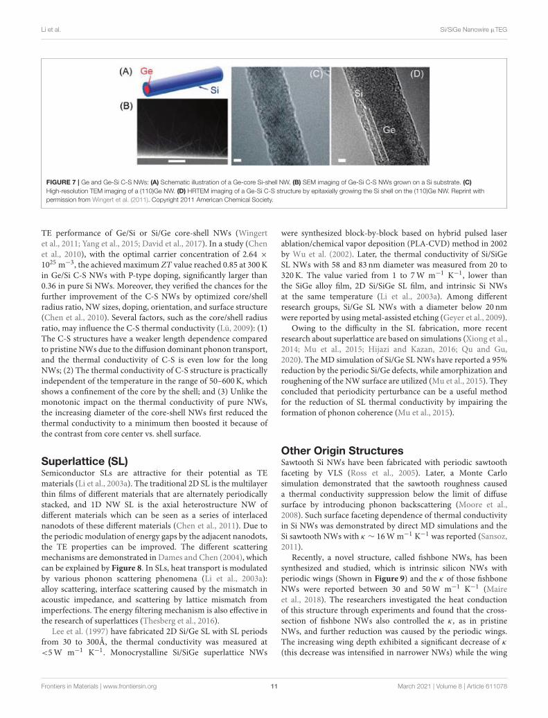
Core-Shell (C-S)The SiGe C-S structure is a radial heterostructure of Si and Ge.SiGe alloys have been used in many electronic devices, such asstressor and high mobility channel materials, for years. Both Geor SiGe layers could be grown selectively in trenches or aroundSiNWs as core layer (Grahn et al., 2000; Hållstedt et al., 2008b;Radamson and Kolahdouz, 2015). The interface between coreand shell reduces thermal conductivity by phonon scattering.A successful synthesis of Ge-Si core-shell NWs with no branchhas been reported recently and the synthesis processes wereelaborated in detail (Noguchi et al., 2016).
Wingert et al. has synthesized sub-20 nm diameters Ge andGe-Si C-S NWs by VLS-CVD method (shown in Figure 7;Wingert et al., 2011). Particularly, κ of the C-S NWs at 388Kis 1.1–2.5W m−1 K−1, remarkably reduced from the Ge NWs(2.3–3.9W m−1 K−1).
Some theoretical works have applied first-principlecalculations and Boltzmann transport theory to model the
Frontiers in Materials | www.frontiersin.org 10 March 2021 | Volume 8 | Article 611078
Li et al. Si/SiGe Nanowire µTEG
FIGURE 7 | Ge and Ge-Si C-S NWs: (A) Schematic illustration of a Ge-core Si-shell NW. (B) SEM imaging of Ge-Si C-S NWs grown on a Si substrate. (C)
High-resolution TEM imaging of a (110)Ge NW. (D) HRTEM imaging of a Ge-Si C-S structure by epitaxially growing the Si shell on the (110)Ge NW. Reprint with
permission from Wingert et al. (2011). Copyright 2011 American Chemical Society.
TE performance of Ge/Si or Si/Ge core-shell NWs (Wingertet al., 2011; Yang et al., 2015; David et al., 2017). In a study (Chenet al., 2010), with the optimal carrier concentration of 2.64 ×
1025 m−3, the achieved maximum ZT value reached 0.85 at 300Kin Ge/Si C-S NWs with P-type doping, significantly larger than0.36 in pure Si NWs. Moreover, they verified the chances for thefurther improvement of the C-S NWs by optimized core/shellradius ratio, NW sizes, doping, orientation, and surface structure(Chen et al., 2010). Several factors, such as the core/shell radiusratio, may influence the C-S thermal conductivity (Lü, 2009): (1)The C-S structures have a weaker length dependence comparedto pristine NWs due to the diffusion dominant phonon transport,and the thermal conductivity of C-S is even low for the longNWs; (2) The thermal conductivity of C-S structure is practicallyindependent of the temperature in the range of 50–600K, whichshows a confinement of the core by the shell; and (3) Unlike themonotonic impact on the thermal conductivity of pure NWs,the increasing diameter of the core-shell NWs first reduced thethermal conductivity to a minimum then boosted it because ofthe contrast from core center vs. shell surface.
Superlattice (SL)Semiconductor SLs are attractive for their potential as TEmaterials (Li et al., 2003a). The traditional 2D SL is the multilayerthin films of different materials that are alternately periodicallystacked, and 1D NW SL is the axial heterostructure NW ofdifferent materials which can be seen as a series of interlacednanodots of these different materials (Chen et al., 2011). Due tothe periodic modulation of energy gaps by the adjacent nanodots,the TE properties can be improved. The different scatteringmechanisms are demonstrated in Dames and Chen (2004), whichcan be explained by Figure 8. In SLs, heat transport is modulatedby various phonon scattering phenomena (Li et al., 2003a):alloy scattering, interface scattering caused by the mismatch inacoustic impedance, and scattering by lattice mismatch fromimperfections. The energy filtering mechanism is also effective inthe research of superlattices (Thesberg et al., 2016).
Lee et al. (1997) have fabricated 2D Si/Ge SL with SL periodsfrom 30 to 300Å, the thermal conductivity was measured at<5W m−1 K−1. Monocrystalline Si/SiGe superlattice NWs
were synthesized block-by-block based on hybrid pulsed laserablation/chemical vapor deposition (PLA-CVD) method in 2002by Wu et al. (2002). Later, the thermal conductivity of Si/SiGeSL NWs with 58 and 83 nm diameter was measured from 20 to320K. The value varied from 1 to 7W m−1 K−1, lower thanthe SiGe alloy film, 2D Si/SiGe SL film, and intrinsic Si NWsat the same temperature (Li et al., 2003a). Among differentresearch groups, Si/Ge SL NWs with a diameter below 20 nmwere reported by usingmetal-assisted etching (Geyer et al., 2009).
Owing to the difficulty in the SL fabrication, more recentresearch about superlattice are based on simulations (Xiong et al.,2014; Mu et al., 2015; Hijazi and Kazan, 2016; Qu and Gu,2020). The MD simulation of Si/Ge SL NWs have reported a 95%reduction by the periodic Si/Ge defects, while amorphization androughening of the NW surface are utilized (Mu et al., 2015). Theyconcluded that periodicity perturbance can be a useful methodfor the reduction of SL thermal conductivity by impairing theformation of phonon coherence (Mu et al., 2015).
Other Origin StructuresSawtooth Si NWs have been fabricated with periodic sawtoothfaceting by VLS (Ross et al., 2005). Later, a Monte Carlosimulation demonstrated that the sawtooth roughness causeda thermal conductivity suppression below the limit of diffusesurface by introducing phonon backscattering (Moore et al.,2008). Such surface faceting dependence of thermal conductivityin Si NWs was demonstrated by direct MD simulations and theSi sawtooth NWs with κ ∼ 16Wm−1 K−1 was reported (Sansoz,2011).
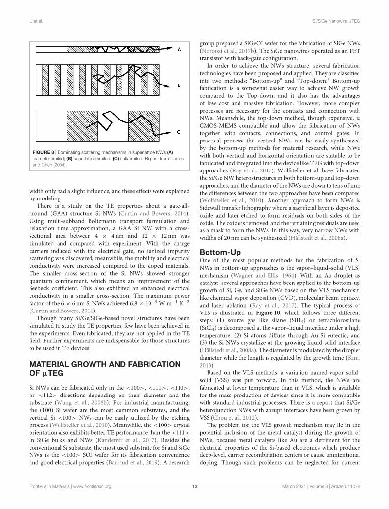
Recently, a novel structure, called fishbone NWs, has beensynthesized and studied, which is intrinsic silicon NWs withperiodic wings (Shown in Figure 9) and the κ of those fishboneNWs were reported between 30 and 50W m−1 K−1 (Maireet al., 2018). The researchers investigated the heat conductionof this structure through experiments and found that the cross-section of fishbone NWs also controlled the κ , as in pristineNWs, and further reduction was caused by the periodic wings.The increasing wing depth exhibited a significant decrease of κ
(this decrease was intensified in narrower NWs) while the wing
Frontiers in Materials | www.frontiersin.org 11 March 2021 | Volume 8 | Article 611078
Li et al. Si/SiGe Nanowire µTEG
FIGURE 8 | Dominating scattering mechanisms in superlattice NWs (A)
diameter limited; (B) superlattice limited; (C) bulk limited. Reprint from Dames
and Chen (2004).
width only had a slight influence, and these effects were explainedby modeling.
There is a study on the TE properties about a gate-all-around (GAA) structure Si NWs (Curtin and Bowers, 2014).Using multi-subband Boltzmann transport formulation andrelaxation time approximation, a GAA Si NW with a cross-sectional area between 4 × 4 nm and 12 × 12 nm wassimulated and compared with experiment. With the chargecarriers induced with the electrical gate, no ionized impurityscattering was discovered; meanwhile, the mobility and electricalconductivity were increased compared to the doped materials.The smaller cross-section of the Si NWs showed strongerquantum confinement, which means an improvement of theSeebeck coefficient. This also exhibited an enhanced electricalconductivity in a smaller cross-section. The maximum powerfactor of the 6 × 6 nm Si NWs achieved 6.8 × 10⁻³ Wm−1 K−2
(Curtin and Bowers, 2014).Though many Si/Ge/SiGe-based novel structures have been
simulated to study the TE properties, few have been achieved inthe experiments. Even fabricated, they are not applied in the TEfield. Further experiments are indispensable for those structuresto be used in TE devices.
MATERIAL GROWTH AND FABRICATIONOF µTEG
Si NWs can be fabricated only in the <100>, <111>, <110>,or <112> directions depending on their diameter and thesubstrate (Wang et al., 2008b). For industrial manufacturing,the (100) Si wafer are the most common substrates, and thevertical Si <100> NWs can be easily utilized by the etchingprocess (Wolfsteller et al., 2010). Meanwhile, the <100> crystalorientation also exhibits better TE performance than the <111>in SiGe bulks and NWs (Kandemir et al., 2017). Besides theconventional Si substrate, the most used substrate for Si and SiGeNWs is the <100> SOI wafer for its fabrication convenienceand good electrical properties (Barraud et al., 2019). A research
group prepared a SiGeOI wafer for the fabrication of SiGe NWs(Noroozi et al., 2017b). The SiGe nanowires operated as an FETtransistor with back-gate configuration.
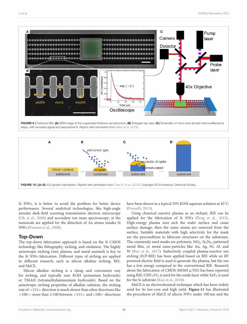
In order to achieve the NWs structure, several fabricationtechnologies have been proposed and applied. They are classifiedinto two methods: “Bottom-up” and “Top-down.” Bottom-upfabrication is a somewhat easier way to achieve NW growthcompared to the Top-down, and it also has the advantagesof low cost and massive fabrication. However, more complexprocesses are necessary for the contacts and connection withNWs. Meanwhile, the top-down method, though expensive, isCMOS-MEMS compatible and allow the fabrication of NWstogether with contacts, connections, and control gates. Inpractical process, the vertical NWs can be easily synthesizedby the bottom-up methods for material research, while NWswith both vertical and horizontal orientation are suitable to befabricated and integrated into the device like TEG with top-downapproaches (Ray et al., 2017). Wolfsteller et al. have fabricatedthe Si/Ge NW heterostructures in both bottom-up and top-downapproaches, and the diameter of the NWs are down to tens of nm;the differences between the two approaches have been compared(Wolfsteller et al., 2010). Another approach to form NWs isSidewall transfer lithography where a sacrificial layer is depositedoxide and later etched to form residuals on both sides of theoxide. The oxide is removed, and the remaining residuals are usedas a mask to form the NWs. In this way, very narrow NWs withwidths of 20 nm can be synthesized (Hållstedt et al., 2008a).
Bottom-UpOne of the most popular methods for the fabrication of SiNWs in bottom-up approaches is the vapor–liquid–solid (VLS)mechanism (Wagner and Ellis, 1964). With an Au droplet ascatalyst, several approaches have been applied to the bottom-upgrowth of Si, Ge, and SiGe NWs based on the VLS mechanismlike chemical vapor deposition (CVD), molecular beam epitaxy,and laser ablation (Ray et al., 2017). The typical process ofVLS is illustrated in Figure 10, which follows three differentsteps: (1) source gas like silane (SiH4) or tetrachlorosilane(SiCl4) is decomposed at the vapor–liquid interface under a hightemperature, (2) Si atoms diffuse through Au-Si eutectic, and(3) the Si NWs crystallize at the growing liquid-solid interface(Hållstedt et al., 2008a). The diameter is modulated by the dropletdiameter while the length is regulated by the growth time (Kim,2013).
Based on the VLS methods, a variation named vapor-solid-solid (VSS) was put forward. In this method, the NWs arefabricated at lower temperature than in VLS, which is availablefor the mass production of devices since it is more compatiblewith standard industrial processes. There is a report that Si/Geheterojunction NWs with abrupt interfaces have been grown byVSS (Chou et al., 2012).
The problem for the VLS growth mechanism may lie in thepotential inclusion of the metal catalyst during the growth ofNWs, because metal catalysts like Au are a detriment for theelectrical properties of the Si-based electronics which producedeep-level, carrier recombination centers or cause unintentionaldoping. Though such problems can be neglected for current
Frontiers in Materials | www.frontiersin.org 12 March 2021 | Volume 8 | Article 611078
Li et al. Si/SiGe Nanowire µTEG
FIGURE 9 | Fishbone NW. (A) SEM image of the suspended fishbone nanostructure; (B) Enlarged top view; (C) Schematic of micro time domain thermoreflectance
setup, with recorded signal and exponential fit. Reprint with permission from Maire et al. (2018).
FIGURE 10 | (A–D) VLS growth mechanism. Reprint with permission from Chen R. et al. (2019). Copyright 2019 American Chemical Society.
Si NWs, it is better to avoid the problem for better deviceperformance. Several analytical technologies, like high-angleannular dark-field scanning transmission electron microscopy(Oh et al., 2008) and secondary ion mass spectroscopy, at thenanoscale are applied for the detection of Au atoms insides SiNWs (Putnam et al., 2008).
Top-DownThe top-down fabrication approach is based on the Si CMOStechnology like lithography, etching, and oxidation. The highlyanisotropic etching (wet, plasma, and metal assisted) is key tothe Si NWs fabrication. Different types of etching are appliedin different research, such as silicon alkaline etching, RIE,and MaCE.
Silicon alkaline etching is a cheap and convenient wayfor etching, and typically uses KOH (potassium hydroxide)or TMAH (tetramethylammonium hydroxide). Based on theanisotropic etching properties of alkaline solution, the etchingrate of<111> direction is much slower than other directions like<100>: more than 1/100 between <111> and<100> directions
have been shown in a typical 35% KOH aqueous solution at 43◦C(Pennelli, 2015).
Using chemical reactive plasma as an etchant, RIE can beapplied for the fabrication of Si NWs (Peng et al., 2015).High-energy plasma ions etch the wafer surface and causesurface damage, then the outer atoms are removed from thesurface. Suitable materials with high selectivity for the maskare the precondition to fabricate structures on the substrates.The commonly used masks are polymers, SiO2, Si3N4, patternedmetal film, or metal nano-particles like Au, Ag, Ni, Al, andW (Ray et al., 2017). Inductively coupled plasma-reactive ionetching (ICP-RIE) has been applied based on RIE while an RFpowered electric field is used to generate the plasma, but the ionhas a low energy compared to the conventional RIE. Researchabout the fabrication of CMOS-MEMS µTEG has been reportedusing RIE; CHF3/O2 is used for the oxide layer while XeF2 is usedfor the Si substrate (Kao et al., 2010).
MaCE is an electrochemical technique which has been widelyused for its low-cost and high yield. Figure 11 has illustratedthe procedures of MaCE of silicon NWs under 100 nm and the
Frontiers in Materials | www.frontiersin.org 13 March 2021 | Volume 8 | Article 611078
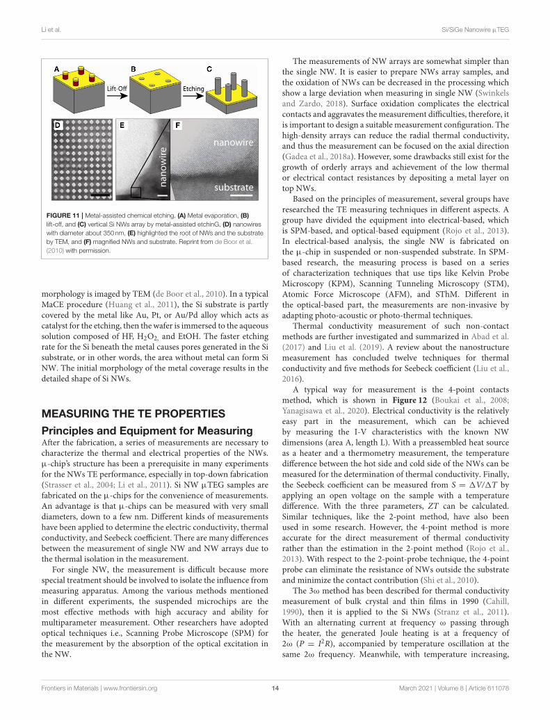
Li et al. Si/SiGe Nanowire µTEG
FIGURE 11 | Metal-assisted chemical etching. (A) Metal evaporation, (B)
lift-off, and (C) vertical Si NWs array by metal-assisted etchinG, (D) nanowires
with diameter about 350 nm, (E) highlighted the root of NWs and the substrate
by TEM, and (F) magnified NWs and substrate. Reprint from de Boor et al.
(2010) with permission.
morphology is imaged by TEM (de Boor et al., 2010). In a typicalMaCE procedure (Huang et al., 2011), the Si substrate is partlycovered by the metal like Au, Pt, or Au/Pd alloy which acts ascatalyst for the etching, then the wafer is immersed to the aqueoussolution composed of HF, H2O2, and EtOH. The faster etchingrate for the Si beneath the metal causes pores generated in the Sisubstrate, or in other words, the area without metal can form SiNW. The initial morphology of the metal coverage results in thedetailed shape of Si NWs.
MEASURING THE TE PROPERTIES
Principles and Equipment for MeasuringAfter the fabrication, a series of measurements are necessary tocharacterize the thermal and electrical properties of the NWs.µ-chip’s structure has been a prerequisite in many experimentsfor the NWs TE performance, especially in top-down fabrication(Strasser et al., 2004; Li et al., 2011). Si NW µTEG samples arefabricated on the µ-chips for the convenience of measurements.An advantage is that µ-chips can be measured with very smalldiameters, down to a few nm. Different kinds of measurementshave been applied to determine the electric conductivity, thermalconductivity, and Seebeck coefficient. There are many differencesbetween the measurement of single NW and NW arrays due tothe thermal isolation in the measurement.
For single NW, the measurement is difficult because morespecial treatment should be involved to isolate the influence frommeasuring apparatus. Among the various methods mentionedin different experiments, the suspended microchips are themost effective methods with high accuracy and ability formultiparameter measurement. Other researchers have adoptedoptical techniques i.e., Scanning Probe Microscope (SPM) forthe measurement by the absorption of the optical excitation inthe NW.
The measurements of NW arrays are somewhat simpler thanthe single NW. It is easier to prepare NWs array samples, andthe oxidation of NWs can be decreased in the processing whichshow a large deviation when measuring in single NW (Swinkelsand Zardo, 2018). Surface oxidation complicates the electricalcontacts and aggravates the measurement difficulties, therefore, itis important to design a suitable measurement configuration. Thehigh-density arrays can reduce the radial thermal conductivity,and thus the measurement can be focused on the axial direction(Gadea et al., 2018a). However, some drawbacks still exist for thegrowth of orderly arrays and achievement of the low thermalor electrical contact resistances by depositing a metal layer ontop NWs.
Based on the principles of measurement, several groups haveresearched the TE measuring techniques in different aspects. Agroup have divided the equipment into electrical-based, whichis SPM-based, and optical-based equipment (Rojo et al., 2013).In electrical-based analysis, the single NW is fabricated onthe µ-chip in suspended or non-suspended substrate. In SPM-based research, the measuring process is based on a seriesof characterization techniques that use tips like Kelvin ProbeMicroscopy (KPM), Scanning Tunneling Microscopy (STM),Atomic Force Microscope (AFM), and SThM. Different inthe optical-based part, the measurements are non-invasive byadapting photo-acoustic or photo-thermal techniques.
Thermal conductivity measurement of such non-contactmethods are further investigated and summarized in Abad et al.(2017) and Liu et al. (2019). A review about the nanostructuremeasurement has concluded twelve techniques for thermalconductivity and five methods for Seebeck coefficient (Liu et al.,2016).
A typical way for measurement is the 4-point contactsmethod, which is shown in Figure 12 (Boukai et al., 2008;Yanagisawa et al., 2020). Electrical conductivity is the relativelyeasy part in the measurement, which can be achievedby measuring the I-V characteristics with the known NWdimensions (area A, length L). With a preassembled heat sourceas a heater and a thermometry measurement, the temperaturedifference between the hot side and cold side of the NWs can bemeasured for the determination of thermal conductivity. Finally,the Seebeck coefficient can be measured from S = 1V/1T byapplying an open voltage on the sample with a temperaturedifference. With the three parameters, ZT can be calculated.Similar techniques, like the 2-point method, have also beenused in some research. However, the 4-point method is moreaccurate for the direct measurement of thermal conductivityrather than the estimation in the 2-point method (Rojo et al.,2013). With respect to the 2-point-probe technique, the 4-pointprobe can eliminate the resistance of NWs outside the substrateand minimize the contact contribution (Shi et al., 2010).
The 3ω method has been described for thermal conductivitymeasurement of bulk crystal and thin films in 1990 (Cahill,1990), then it is applied to the Si NWs (Stranz et al., 2011).With an alternating current at frequency ω passing throughthe heater, the generated Joule heating is at a frequency of2ω (P = I2R), accompanied by temperature oscillation at thesame 2ω frequency. Meanwhile, with temperature increasing,
Frontiers in Materials | www.frontiersin.org 14 March 2021 | Volume 8 | Article 611078

Li et al. Si/SiGe Nanowire µTEG
FIGURE 12 | Typical 4-point probe method for TE measurement.Reprint from
Boukai et al. (2008).
the resistance is increased by a 2ω oscillation. Thus, there isa 3ω oscillation component of the voltage (V = IR) acrossthe heater, and the thermal conductivity can be calculated bymeasuring this component (Lu et al., 2001). A similar 2ωtechnique combined four-probe microchip has been put forwardso that the Seebeck coefficient can also be attained by the equationS = 1V(2ω)/1T(2ω), while the 1V(2ω) is the Seebeck voltageinduced by the temperature difference from the ac current atfrequency ω through a micro-heater (Kirihara et al., 2011).
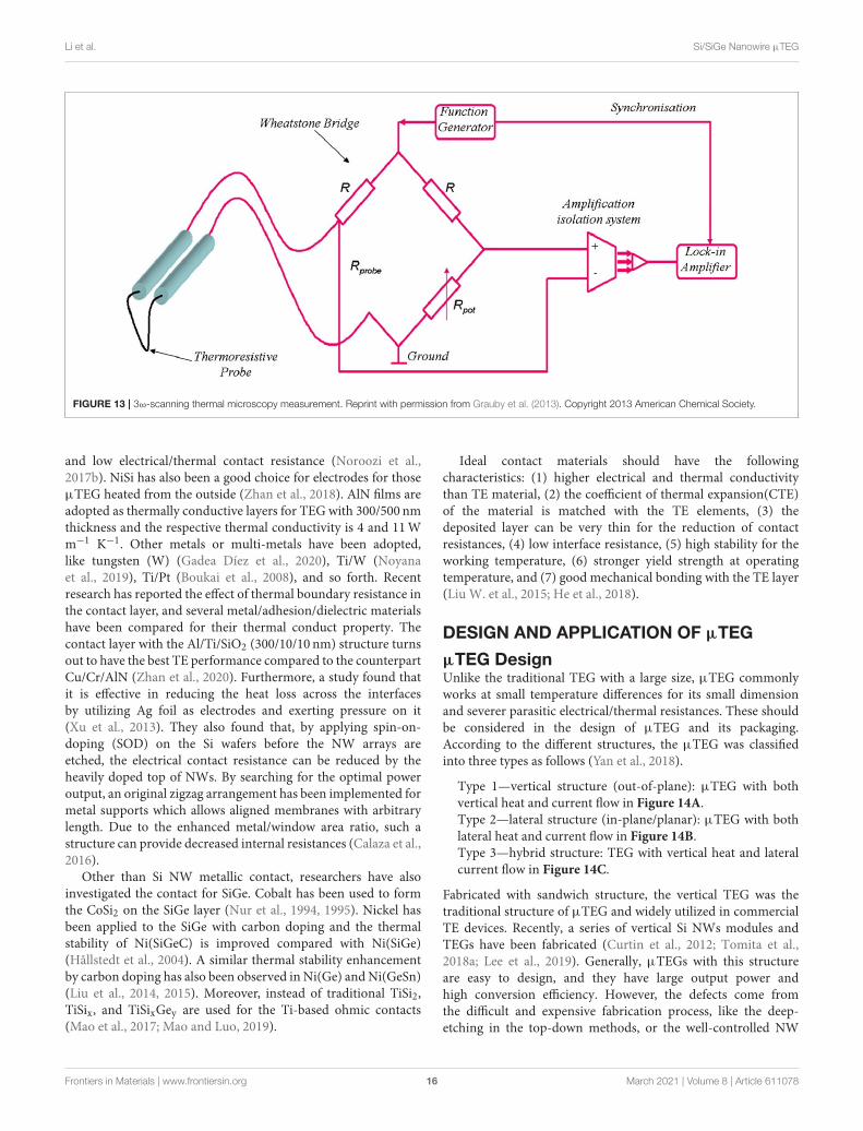
An alternative method for TE properties is the SPM. In thiskind of technique, probes or tips are used for scanning the NWswith nanometric resolution. The surface topography of samplescan be imaged by the probe. With high spatial resolution, SPMare utilized for measurements of both electrical and thermalconductivities. For NWs electrical conductivity measurement,the AFM and STM are typically used, while SThM combinedwith the 3ω method can be used for thermal conductivitymeasurement (Grauby et al., 2013), shown in Figure 13.
TE Properties for NWs and TEGThe first measured thermal conductivity of silicon NWs wasachieved in 2003, and found a small value of κ down to 7–8W m−1 K−1 for NWs 22 nm wide with the VLS method (Liet al., 2003b). Compared to 20 nm thickness Si film with thermalconductivity∼ 22Wm−1 K−1, a reduction of around two-thirdsof the thermal conductivity was observed, and the value becomessmaller than measured suspended films down to a thickness of∼10 nm with thermal conductivity ∼10W m−1 K−1. For themeasurement, they used microfabricated suspended plates forthe positioning of the individual NW, where Pt resistors wereintegrated in the TEG as electrodes, heater, and thermometer; thismethod has been adopted inmany studies. Following, Hochbaumet al. used 50 nm NWs fabricated by MaCE and demonstrateda very small κ of 1.6W m−1 K−1 where the phonon thermalconductivity κph was estimated about 1W m−1 K−1. This is5–8 times lower than the corresponding Si NWs synthesizedby the VLS method (Hochbaum et al., 2008). The reduction
was explained by the phonon surface scattering effect, sinceMaCE NWs exhibited a rougher surface compared to VLS NWs(Pennelli, 2015). Later, more research reports about Si NWs havereported the thermal conductivity based on different equipment.A TE module based on vertical rough Si NWs with 200 nmdiameter showed the lowest thermal conductivity between 10.1and 14.8W m−1 K−1 with boron- and phosphorus-doped,and the Pmax was 3.74 µW/cm2 with temperature difference1T = 180K (Lee et al., 2019). For different fabrications andmeasurement techniques, the precision in data varies accordingto the literature. And the experiment conditions are constantlychanging and errors may exist. When measuring the samples, itis crucial to select appropriate measurements for accuracy.
For the fabricated µTEG in research, there are severalexperimental data of generated output. A vertical Si NWstructure is demonstrated by RIE with a TE power of 29.3 µWat 1T = 56K under 50 × 50µm chip area; spin-on glass thinfilm is applied for the support of Si NW (Curtin et al., 2012). Anoutput power density of 9 µW/cm2 is measured at 1T = 27Kcross the Si NWs µTEG fabricated by the CVD-VLS methods(Dávila et al., 2012). By standard CMOS processing, 20 thin Simembranes generated an output power density of 4.5 µW/cm2
under1T= 5K by using 20 thin Si membranesmadeµTEGwitharea of 50× 150µm on the chip (Perez-Marín et al., 2014). Morerecently, Donmez et al. have measured the maximum powerdensities of Si NWs, SiGe NWs, and Si micro-beam-based µTEGwith values of 41.2, 45.2, and 34.5 µW/ cm2, respectively, at ahot plate temperature of 100◦C (Donmez Noyan et al., 2019).A two-leg µTEG has been fabricated based on vertical Si NWforest where the achieved power output is 0.25–0.5 µW/(cm2K2)with the NW length from 25 to 6.5µm (Elyamny et al., 2020).By shortening Si NW to sub-µm length, a planar µTEG achievedthe power density of 12 µW/cm2 with 1T = 5K (Tomita et al.,2018b).
Simulations and analytic models based on the finite elementmethod (FEM) have been applied for the risk/cost reduction infabrication, and the data are compared with the experimentalresults (Tomita et al., 2018b; DonmezNoyan et al., 2019; Elyamnyet al., 2020). In a recent study, with the 3-D FEM devicesimulation software COMSOL Multiphysics, a research grouphas analyzed the thermal distribution and power generationof Si NWs TEG with varied parameters (Zhang et al., 2018).An extreme high-power density of 4.2 and 425 mW/cm2 wasachieved in the simulation at 0.1 × 0.1µm Si NWs, respectively,under 1T = 5 and 57K. With the model, maximum powergeneration density is speculated to be proportional to 1T2.
Thermal and Electrical Contact ResistanceThe electrical and thermal contact resistance of the metalelectrodes are special issues for measurement which have severeimpacts on the nanodevice performance which mean that ohmiccontacts are necessary. Following the scaling of IC-technology,different metal electrodes have been experimented on for thecontact resistance with the tendency of TiSi2 → CoSi2 →
Ni(Pt)Si in planar structures (Lavoie et al., 2017). For thefabrication of µTEG integrated with a heater, Pt is a good choicefor both electrodes and heaters due to its thermal-independence
Frontiers in Materials | www.frontiersin.org 15 March 2021 | Volume 8 | Article 611078
Li et al. Si/SiGe Nanowire µTEG
FIGURE 13 | 3ω-scanning thermal microscopy measurement. Reprint with permission from Grauby et al. (2013). Copyright 2013 American Chemical Society.
and low electrical/thermal contact resistance (Noroozi et al.,2017b). NiSi has also been a good choice for electrodes for thoseµTEG heated from the outside (Zhan et al., 2018). AlN films areadopted as thermally conductive layers for TEG with 300/500 nmthickness and the respective thermal conductivity is 4 and 11Wm−1 K−1. Other metals or multi-metals have been adopted,like tungsten (W) (Gadea Díez et al., 2020), Ti/W (Noyanaet al., 2019), Ti/Pt (Boukai et al., 2008), and so forth. Recentresearch has reported the effect of thermal boundary resistance inthe contact layer, and several metal/adhesion/dielectric materialshave been compared for their thermal conduct property. Thecontact layer with the Al/Ti/SiO2 (300/10/10 nm) structure turnsout to have the best TE performance compared to the counterpartCu/Cr/AlN (Zhan et al., 2020). Furthermore, a study found thatit is effective in reducing the heat loss across the interfacesby utilizing Ag foil as electrodes and exerting pressure on it(Xu et al., 2013). They also found that, by applying spin-on-doping (SOD) on the Si wafers before the NW arrays areetched, the electrical contact resistance can be reduced by theheavily doped top of NWs. By searching for the optimal poweroutput, an original zigzag arrangement has been implemented formetal supports which allows aligned membranes with arbitrarylength. Due to the enhanced metal/window area ratio, such astructure can provide decreased internal resistances (Calaza et al.,2016).
Other than Si NW metallic contact, researchers have alsoinvestigated the contact for SiGe. Cobalt has been used to formthe CoSi2 on the SiGe layer (Nur et al., 1994, 1995). Nickel hasbeen applied to the SiGe with carbon doping and the thermalstability of Ni(SiGeC) is improved compared with Ni(SiGe)(Hållstedt et al., 2004). A similar thermal stability enhancementby carbon doping has also been observed in Ni(Ge) andNi(GeSn)(Liu et al., 2014, 2015). Moreover, instead of traditional TiSi2,TiSix, and TiSixGey are used for the Ti-based ohmic contacts(Mao et al., 2017; Mao and Luo, 2019).
Ideal contact materials should have the followingcharacteristics: (1) higher electrical and thermal conductivitythan TE material, (2) the coefficient of thermal expansion(CTE)of the material is matched with the TE elements, (3) thedeposited layer can be very thin for the reduction of contactresistances, (4) low interface resistance, (5) high stability for theworking temperature, (6) stronger yield strength at operatingtemperature, and (7) good mechanical bonding with the TE layer(Liu W. et al., 2015; He et al., 2018).
DESIGN AND APPLICATION OF µTEG
µTEG DesignUnlike the traditional TEG with a large size, µTEG commonlyworks at small temperature differences for its small dimensionand severer parasitic electrical/thermal resistances. These shouldbe considered in the design of µTEG and its packaging.According to the different structures, the µTEG was classifiedinto three types as follows (Yan et al., 2018).
Type 1—vertical structure (out-of-plane): µTEG with bothvertical heat and current flow in Figure 14A.Type 2—lateral structure (in-plane/planar): µTEG with bothlateral heat and current flow in Figure 14B.Type 3—hybrid structure: TEG with vertical heat and lateralcurrent flow in Figure 14C.
Fabricated with sandwich structure, the vertical TEG was thetraditional structure of µTEG and widely utilized in commercialTE devices. Recently, a series of vertical Si NWs modules andTEGs have been fabricated (Curtin et al., 2012; Tomita et al.,2018a; Lee et al., 2019). Generally, µTEGs with this structureare easy to design, and they have large output power andhigh conversion efficiency. However, the defects come fromthe difficult and expensive fabrication process, like the deep-etching in the top-down methods, or the well-controlled NW
Frontiers in Materials | www.frontiersin.org 16 March 2021 | Volume 8 | Article 611078

Li et al. Si/SiGe Nanowire µTEG
FIGURE 14 | Three types of µTEG. (A) Vertical structure; (B) lateral structure; (C) hybrid structure. Reprint with permission from Yan et al. (2018).
synthesis and metal electrodes integration in the bottom-upmethods (Zhan et al., 2018). The lateral structureµTEG, which iscompatible with the CMOS process, is relatively easy to fabricate(Xie et al., 2010; Yu et al., 2012, 2015; Noroozi et al., 2017b).But the drawbacks lie in the comparatively low efficiency owingto high parasitic heat flux and low temperature difference. Forthat reason, the lateral structure is unable to be utilized inpower generation and often applied in different sensors. As acompromise of the abovementioned two structures, the hybridstructure shows integrated advantages. In the hybrid structure,the heat flux from ambient flows vertically in a planar direction,and is ejected vertically from another side (Xie et al., 2010).Therefore, the hybrid structure µTEG is desirable to satisfyparticular applications and the key for the optimization is thedesign of a heat flux path.
Moreover, the substrates are etched away to form thermallyisolated Si NWs for high efficacy, resulting in a vulnerablestructure and expensive fabrication cost. Generally, the highconversion efficiency is essential when the expensive specifiedheat source is applied, such as RTG, while power generationdensity is crucial for the heat source which is cheap or free, likewaste heat (Zhan et al., 2018).
Performance and ApplicationIn fact, the first generation of TEG, the radioisotope TEG, hasbeen used during the last four decades for power supply byconverting the thermal power generated by a radioisotope heatsource to electricity for many planetary exploration missions.
Unlike a solar power generator, the RTG can operate withoutsunlight. That advantage fits well with long (more than 10 years)and far-distanced missions (O’Brien et al., 2008).
The µTEGs are a terrific power source for existing andcoming electronics considering their ubiquity, magnitude ofheat dissipation, and the direct, stable, and non-pollutive energyconversion. The aim of µTEG research is to supply steadyelectricity power for those miniature electronic instruments. Acomparison of the existing microgenerators and applications hasbeen exhibited in Figure 15 (Iannacci, 2019). After the researchinto TEG and boom of electrical technology, µTEGs have cometo be utilized in many fields, like business electronics, healthelectronics, and IoT (Haras and Skotnicki, 2018; Tomita et al.,2018a). For business electronics, the milestone application ofµTEGwas a TE watch named Thermatron which was introducedby Bulova in 1980; however it failed due to its unreliable batteryand high price (Adams, 2019). A recent smart watch namedMatrix Powerwatch II, which is powered by body temperature,has the like calorie counting, sleep tracker, and step counting(Powerwatch, 2020).
Heat dissipation from the human body has been considered asan excellent source of heat energy. As the skin on the wrist has arelatively constant temperature of 36.5◦C, it would be possible toutilize this heat for wearable TEGs (Lv et al., 2016). Meanwhile,the temperature difference between the skin and the internalbody can reach a maximum of 8◦C, sufficient to generate amicrowatt level of electricity with µTEG (Ben Amar et al., 2015).It can serve as an alternative power supply compared to other
Frontiers in Materials | www.frontiersin.org 17 March 2021 | Volume 8 | Article 611078

Li et al. Si/SiGe Nanowire µTEG
FIGURE 15 | (A) Exsiting microgenerator; (B) Typical low-power devices. Reprint from Iannacci (2019).
conventional power sources in many wearable devices, especiallywith implant medical devices like pacemakers (Siddique et al.,2017). For IMD, the difficulty is the permanent operation orstandby of the electronics with no secondary removal; body heatis a perfect endless source for those devices like pacemakers.
The increase of research into IoT has also promoted theapplication of µTEG. The IoT calls for smart, integrated,miniaturized, and low-energy wireless nodes, powered by non-renewable batteries in most cases. The most important part ofIoT is the discrete wireless sensor networks (WSNs) which aredistributed in different fields like intelligent buildings, medicaltreatment, monitoring, and security (Ghayvat et al., 2015). Thelow power dissipation (10–104 µW/cm2) corresponds with thepower supplied by µTEG (Noyana et al., 2019). A TE energy
harvesting system for WSN has been designed with an inputpower of 84 µW (Guan et al., 2017). Designed for buildingenergy management (BEM), a TEG-powered WSNs module hasbeen built and characterized in a recent study, which shows thepossibility for further application of µTEG for WSNs (Wanget al., 2013).
Some problems limited the application for µTEG and needbetter solutions. Above all, the conversion efficiency of energyis around 5–10% owing to the low ZT of TE materials (mostly<1), which is much lower than traditional generators and hasno market competitiveness. Secondly, it is difficult to attainhigh temperature differences in daily life; for a wearable TEG,the typical 1T is 5–15◦C. Finally, a suitable external load isneeded for load matching and power matching (Siddique et al.,
Frontiers in Materials | www.frontiersin.org 18 March 2021 | Volume 8 | Article 611078
Li et al. Si/SiGe Nanowire µTEG
FIGURE 16 | Hierarchical requirements for TEG: the
efficiency–effectiveness–reliability mountain. Reprint from Liu W. et al. (2015).
2017).More requirements of TEG can be illustrated by Figure 16,which is also essential for µTEG. A good TE power systemshould possess all three demands as a minimum: efficiency,effectiveness, and reliability (Liu W. et al., 2015). More detailedrequirements should be considered like strong device bondingstrength, excellent thermal stability, and chemical stability.
SUMMARY AND PROSPECT
In this review article, we have explored the basic conceptionsin the fabrication of Si-based NW µTEG. The µTEG hasa bright future as an efficient method for power supplyin wireless microelectronic devices due to its energy recycleand convenience. However, there are still many problemsthat must be addressed before proceeding to large-scaleapplication. Among those TE properties that influence ZT,thermal conductivity κ is the most important parameter inthe consideration for the design of µTEG with Si and SiGeNWs. Most research is focusing on the tuning of phononthermal conductivity, which is dominant in semiconductors.Then the novel potential materials in Group IV have been stated;
specifically we explain the superiority of Si and SiGe NWs asa candidate for TEs. Simple examples for the novel structurein the SiGe NWs e.g., superlattice (SL), core-shell (C-S), etc.,have been presented for their possibility to further enhance theTE properties. The methods for fabrication are also introducedin this article, with the top-down and bottom-up methodsillustrated and the detailed process generalized like MBE, RIE,and STL. After the process, the analysis and characterization ofTE in different articles about the TE parameters are reviewedhere, the commonly used 4-point probing for the electricalproperties with I-V characteristic curve described and 3ωmethod for the thermal conductivity. Finally, we describe theexisting and prospective applications for TEG-sourced devices,which are likely to be an enormous market in the near future.For the utilization of µTEG, IoT is a good carrier due to itsminiature energy consumption. Also, flexible wearable devicesand implantable medical devices are promising directions.
We believe more research is necessary to further enhancethe TE properties and lower the cost of processing and powergenerating. From this research, Si and SiGe NW µTEGs have thepotential to find their niche in daily life and in more complicatedapplication scenarios.
AUTHOR CONTRIBUTIONS
YL and HR conceived and designed the manuscript. YL wrotethe article. GW, MA-S, MP, and HR revised it. All authorscontributed to the article and approved the submitted version.
FUNDING
This work was supported by the construction of high-levelinnovation research institute from the Guangdong GreaterBay Area Institute of Integrated Circuit and System (GrantNo. 2019B090909006) and the projects of the constructionof new research and development institutions (Grant No.2019B090904015), in part by the the National Key Research andDevelopment Program of China (Grant No. 2016YFA0301701),the Youth Innovation Promotion Association of CAS (GrantNo. Y2020037), and the National Natural Science Foundation ofChina (Grant No. 92064002).
ACKNOWLEDGMENTS
Financial support from the Institute of Microelectronics, ChineseAcademic of Science and Guangdong Greater Bay Area Instituteof Integrated Circuit and System is gratefully acknowledged.
REFERENCES
Abad, B., Borca-Tasciuc, D. A., and Martin-Gonzalez, M. S. (2017). Non-contactmethods for thermal properties measurement. Renew. Sustain. Energy Rev. 76,1348–1370. doi: 10.1016/j.rser.2017.03.027
Adams, A. (2019). Bulova Thermatron Watch Hands-On: The Temperature-
Powered Timepiece That Never Was. Available online at: https://www.
ablogtowatch.com/bulova-thermatron-watch-temperature-powered-timepiece/
Akbari-Saatlu, M., Procek, M., Mattsson, C., Thungstrom, G., Nilsson, H.E., Xiong, W., et al. (2020). Silicon nanowires for gas sensing: a review.Nanomaterials 10:2215. doi: 10.3390/nano10112215
Bahk, J.-H., Bian, Z., and Shakouri, A. (2013). Electron energy filteringby a nonplanar potential to enhance the thermoelectric power factor
Frontiers in Materials | www.frontiersin.org 19 March 2021 | Volume 8 | Article 611078

Li et al. Si/SiGe Nanowire µTEG
in bulk materials. Phys. Rev. B 87:075204. doi: 10.1103/PhysRevB.87.075204
Barraud, S., Previtali, B., Lapras, V., Coquand, R., Vizioz, C., Hartmann, J. M.,et al. (2019). Top-down fabrication and electrical characterization of Si andSiGe nanowires for advanced CMOS technologies. Semicond. Sci. Technol.34:074001. doi: 10.1088/1361-6641/ab1e5b
Ben Amar, A., Kouki, A. B., and Cao, H. (2015). Power approaches for implantablemedical devices. Sensors 15, 28889–28914. doi: 10.3390/s151128889
Bennett, N. S., Byrne, D., and Cowley, A. (2015). Enhanced Seebeck coefficientin silicon nanowires containing dislocations. Appl. Phys. Lett. 107:013903.doi: 10.1063/1.4926331
Borup, K. A., de Boor, J., Wang, H., Drymiotis, F., Gascoin, F., Shi, X., et al. (2015).Measuring thermoelectric transport properties of materials. Energy Environ.
Sci. 8, 423–435. doi: 10.1039/C4EE01320DBoukai, A. I., Bunimovich, Y., Tahir-Kheli, J., Yu, J. K., Goddard, W. A. III, and
Heath, J. R. (2008). Silicon nanowires as efficient thermoelectric materials.Nature 451, 168–171. doi: 10.1038/nature06458
Cahill, D. G. (1990). Thermal conductivity measurement from 30 to 750 K: the 3ωmethod. Rev. Scient. Instrum. 61, 802–808. doi: 10.1063/1.1141498
Cahill, D. G., Ford, W. K., Goodson, K. E., Mahan, G. D., Majumdar, A., Maris,H. J., et al. (2003). Nanoscale thermal transport. J Appl Phys. 93, 793–818.doi: 10.1063/1.1524305
Calaza, C., Donmez, I., Salleras, M., Gadea, G., Santos, J. D., Morata, A.,et al. (2016). Optimization of power output in planar thermoelectricmicrogenerators based on Si nanowires. J. Phys. Conf. Ser. 773:012026.doi: 10.1088/1742-6596/773/1/012026
Calaza, C., Salleras, M., Dávila, D., Tarancón, A., Morata, A., Santos, J. D.,et al. (2015). Bottom-up silicon nanowire arrays for thermoelectric harvesting.Mater. Today Proc. 2, 675–679. doi: 10.1016/j.matpr.2015.05.085
Chen, J., Zhang, G., and Li, B. (2009). Tunable thermal conductivity of Si1−xGexnanowires. Appl. Phys. Lett. 95:073117. doi: 10.1063/1.3212737
Chen, R., Lee, J., Lee, W., and Li, D. (2019). Thermoelectrics of nanowires. Chem.
Rev. 119, 9260–9302. doi: 10.1021/acs.chemrev.8b00627Chen, S., Li, W., Li, X., and Yang, W. (2019). One-dimensional SiC nanostructures:
designed growth, properties, and applications. Prog. Mater. Sci. 104, 138–214.doi: 10.1016/j.pmatsci.2019.04.004
Chen, X., Wang, Y., and Ma, Y. (2010). High thermoelectric performance ofGe/Si core–shell nanowires: first-principles prediction. J. Phys. Chem. C 114,9096–9100. doi: 10.1021/jp101132u
Chen, X., Wang, Z., and Ma, Y. (2011). Atomistic design of high thermoelectricityon Si/Ge superlattice nanowires. J. Phys. Chem. C 115, 20696–20702.doi: 10.1021/jp2060014
Choi, J. H., Pala, M., Latu-Romain, L., and Bano, E. (2011). Theoretical studyof thermoelectric properties of SiC nanowires. Mater. Sci. Forum. 717–720,561–564. doi: 10.4028/www.scientific.net/MSF.717-720.561
Chou, Y. C., Wen, C. Y., Reuter, M. C., Su, D., Stach, E. A., and Ross, F. M.(2012). Controlling the growth of Si/Ge nanowires and heterojunctions usingsilver-gold alloy catalysts. ACS Nano. 6, 6407–6415. doi: 10.1021/nn301978x
Curtin, B. M., and Bowers, J. E. (2014). Thermoelectric power factorenhancement with gate-all-around silicon nanowires. J. Appl. Phys. 115:143704.doi: 10.1063/1.4870962
Curtin, B. M., Fang, E. W., and Bowers, J. E. (2012). Highly ordered vertical siliconnanowire array composite thin films for thermoelectric devices. J. Electron.Mater. 41, 887–894. doi: 10.1007/s11664-012-1904-1
Dames, C., and Chen, G. (2004). Theoretical phonon thermal conductivity of Si/Gesuperlattice nanowires. J. Appl. Phys. 95, 682–693. doi: 10.1063/1.1631734
David, T., Liu, K., Ronda, A., Favre, L., Abbarchi, M., Gailhanou, M., et al.(2017). Tailoring strain and morphology of core-shell SiGe nanowiresby low-temperature Ge condensation. Nano Lett. 17, 7299–7305.doi: 10.1021/acs.nanolett.7b02832
Dávila, D., Tarancón, A., Calaza, C., Salleras, M., Fernández-Regúlez, M., SanPaulo, A., et al. (2012). Monolithically integrated thermoelectric energyharvester based on silicon nanowire arrays for powering micro/nanodevices.Nano Energy 1, 812–819. doi: 10.1016/j.nanoen.2012.06.006
de Boor, J., Geyer, N., Wittemann, J. V., Gosele, U., and Schmidt, V. (2010). Sub-100 nm silicon nanowires by laser interference lithography and metal-assistedetching. Nanotechnology 21:095302. doi: 10.1088/0957-4484/21/9/095302
Donmez Noyan, I., Dolcet, M., Salleras, M., Stranz, A., Calaza, C., Gadea,G., et al. (2019). All-silicon thermoelectric micro/nanogenerator including aheat exchanger for harvesting applications. J. Power Sources 413, 125–133.doi: 10.1016/j.jpowsour.2018.12.029
Dresselhaus, M. S., Chen, G., Tang, M. Y., Yang, R. G., Lee, H., Wang, D. Z.,et al. (2007). New directions for low-dimensional thermoelectricmaterials.Adv.Mater. 19, 1043–1053. doi: 10.1002/adma.200600527
Elyamny, S., Dimaggio, E.,Magagna, S., Narducci, D., and Pennelli, G. (2020). Highpower thermoelectric generator based on vertical silicon nanowires. Nano Lett.20, 4748–4753. doi: 10.1021/acs.nanolett.0c00227
Feser, J. P., Sadhu, J. S., Azeredo, B. P., Hsu, K. H., Ma, J., Kim, J., et al. (2012).Thermal conductivity of silicon nanowire arrays with controlled roughness. J.Appl. Phys. 112:114306. doi: 10.1063/1.4767456
Gadea Díez, G., Sojo Gordillo, J. M., Pacios Pujadó, M., Salleras, M., Fonseca, L.,Morata, A., et al. (2020). Enhanced thermoelectric figure of merit of individualSi nanowires with ultralow contact resistances. Nano Energy 67:104191.doi: 10.1016/j.nanoen.2019.104191
Gadea, G., Morata, A., and Tarancon, A. (2018a). Semiconductor nanowiresfor thermoelectric generation. Semiconduct. Semimetals 98, 321–407.doi: 10.1016/bs.semsem.2018.01.001
Gadea, G., Pacios, M., Morata, Á., and Tarancón, A. (2018b). Silicon-basednanostructures for integrated thermoelectric generators. J. Phys. D Appl. Phys.51:423001. doi: 10.1088/1361-6463/aad683
Garg, J., Bonini, N., Kozinsky, B., and Marzari, N. (2011). Role ofdisorder and anharmonicity in the thermal conductivity of silicon-germanium alloys: a first-principles study. Phys. Rev. Lett. 106:045901.doi: 10.1103/PhysRevLett.106.045901
Geyer, N., Huang, Z., Fuhrmann, B., Grimm, S., Reiche, M., Nguyen-Duc, T. K.,et al. (2009). Sub-20 nm Si/Ge superlattice nanowires by metal-assisted etching.Nano Lett. 9, 3106–3110. doi: 10.1021/nl900751g
Ghayvat, H., Mukhopadhyay, S., Gui, X., and Suryadevara, N. (2015). WSN- andIOT-based smart homes and their extension to smart buildings. Sensors 15,10350–10379. doi: 10.3390/s150510350
Glassbrenner, C. J., and Slack, G. A. (1964). Thermal conductivity of silicon andgermanium from 3◦K to the melting point. Phys. Rev. 134, A1058–A1069.doi: 10.1103/PhysRev.134.A1058
Goktas, N. I., Wilson, P., Ghukasyan, A., Wagner, D., McNamee, S., and LaPierre,R. R. (2018). Nanowires for energy: a review. Appl. Phys. Rev. 5:041305.doi: 10.1063/1.5054842
Goldsmid, H. J. (2014). Bismuth telluride and its alloys as materials forthermoelectric generation.Materials 7, 2577–2592. doi: 10.3390/ma7042577
Grahn, J. V., Fosshaug, H., Jargelius, M., Jönsson, P., Linder, M., Malm, B.G., et al. (2000). A low-complexity 62-GHz fT SiGe heterojunction bipolartransistor process using differential epitaxy and in situ phosphorus-dopedpoly-Si emitter at very low thermal budget. Solid State Electron. 44, 549–554.doi: 10.1016/S0038-1101(99)00266-X
Grauby, S., Puyoo, E., Rampnoux, J.-M., Rouvière, E., and Dilhaire, S.(2013). Si and SiGe nanowires: fabrication process and thermal conductivitymeasurement by 3ω-scanning thermal microscopy. J. Phys. Chem. C 117,9025–9034. doi: 10.1021/jp4018822
Guan, M., Wang, K., Xu, D., and Liao, W.-H. (2017). Design and experimentalinvestigation of a low-voltage thermoelectric energy harvesting systemfor wireless sensor nodes. Energy Convers. Manage. 138, 30–37.doi: 10.1016/j.enconman.2017.01.049
Hållstedt, J., Blomqvist, M., Persson, P. O. Å., Hultman, L., and Radamson, H.H. (2004). The effect of carbon and germanium on phase transformationof nickel on Si1−x−yGexCy epitaxial layers. J. Appl. Phys. 95, 2397–2402.doi: 10.1063/1.1645996
Hållstedt, J., Hellström, P. E., and Radamson, H. H. (2008a). Sidewalltransfer lithography for reliable fabrication of nanowires and deca-nanometerMOSFETs. Thin Solid Films 517, 117–120. doi: 10.1016/j.tsf.2008.08.134
Hållstedt, J., Kolahdouz, M., Ghandi, R., Radamson, H. H., and Wise, R. (2008b).Pattern dependency in selective epitaxy of B-doped SiGe layers for advancedmetal oxide semiconductor field effect transistors. J. Appl. Phys. 103:054907.doi: 10.1063/1.2832631
Haras, M., and Skotnicki, T. (2018). Thermoelectricity for IoT – a review. NanoEnergy 54, 461–476. doi: 10.1016/j.nanoen.2018.10.013
Frontiers in Materials | www.frontiersin.org 20 March 2021 | Volume 8 | Article 611078

Li et al. Si/SiGe Nanowire µTEG
Harman, T. C., Taylor, P. J., Walsh, M. P., and LaForge, B. E. (2002). Quantumdot superlattice thermoelectric materials and devices. Science 297, 2229–2232.doi: 10.1126/science.1072886
Hattori, J., and Uno, S. (2013). Impact of isotope doping on phononthermal transport in silicon nanowires. Jpn. J. Appl. Phys. 52:04CN04.doi: 10.7567/JJAP.52.04CN04
He, R., Schierning, G., and Nielsch, K. (2018). Thermoelectric devices: a reviewof devices, architectures, and contact optimization. Adv. Mater. Technol.3:1700256. doi: 10.1002/admt.201700256
Heremans, J. P., Jovovic, V., Toberer, E. S., Saramat, A., Kurosaki, K.,Charoenphakdee, A., et al. (2008). Enhancement of thermoelectric efficiencyin PbTe by distortion of the electronic density of states. Science 321, 554–557.doi: 10.1126/science.1159725
Hicks, L. D., and Dresselhaus, M. S. (1993a). Thermoelectric figure of merit of aone-dimensional conductor. Phys. Rev. B Condens. Matter. 47, 16631–16634.doi: 10.1103/PhysRevB.47.16631
Hicks, L. D., and Dresselhaus, M. S. (1993b). Effect of quantum-well structureson the thermoelectric figure of merit. Phys. Rev. B Condens. Matter. 47,12727–12731. doi: 10.1103/PhysRevB.47.12727
Hijazi, M., and Kazan, M. (2016). Phonon heat transport in superlattices: case ofSi/SiGe and SiGe/SiGe superlattices.AIP Adv. 6:065024. doi: 10.1063/1.4955052
Hochbaum, A. I., Chen, R., Delgado, R. D., Liang, W., Garnett, E. C., Najarian, M.,et al. (2008). Enhanced thermoelectric performance of rough silicon nanowires.Nature 451, 163–167. doi: 10.1038/nature06381
Hu, M., Giapis, K. P., Goicochea, J. V., Zhang, X., and Poulikakos, D. (2011).Significant reduction of thermal conductivity in Si/Ge core-shell nanowires.Nano Lett. 11, 618–623. doi: 10.1021/nl103718a
Huang, Z., Geyer, N., Werner, P., de Boor, J., and Gosele, U. (2011). Metal-assistedchemical etching of silicon: a review. Adv. Mater. Weinheim. 23, 285–308.doi: 10.1002/adma.201001784
Huxtable, S. T., Abramson, A. R., Tien, C.-L., Majumdar, A., LaBounty, C., Fan,X., et al. (2002). Thermal conductivity of Si/SiGe and SiGe/SiGe superlattices.Appl. Phys. Lett. 80, 1737–1739. doi: 10.1063/1.1455693
Iannacci, J. (2019). Microsystem based Energy Harvesting (EH-MEMS): poweringpervasivity of the Internet of Things (IoT) – a review with focus on mechanicalvibrations. J. King Saud Univ. Sci. 31, 66–74. doi: 10.1016/j.jksus.2017.05.019
Ishibe, T., Tomeda, A., Watanabe, K., Kamakura, Y., Mori, N., Naruse, N.,et al. (2018). Methodology of thermoelectric power factor enhancement bycontrolling nanowire interface. ACS Appl. Mater. Interfaces 10, 37709–37716.doi: 10.1021/acsami.8b13528
Joshi, G., Lee, H., Lan, Y., Wang, X., Zhu, G., Wang, D., et al. (2008). Enhancedthermoelectric figure-of-merit in nanostructured p-type silicon germaniumbulk alloys. Nano Lett. 8, 4670–4674. doi: 10.1021/nl8026795
Ju, Y. S., and Goodson, K. E. (1999). Phonon scattering in silicon filmswith thickness of order 100 nm. Appl. Phys. Lett. 74, 3005–3007.doi: 10.1063/1.123994
June, F., and Zakrajsek, D. F. W. (2017). Jean-Pierre Fleurial NASA Special Session:
Next-Generation Radiaisotope Thermoelectric Generator Discussion.
Kandemir, A., Ozden, A., Cagin, T., and Sevik, C. (2017). Thermal conductivityengineering of bulk and one-dimensional Si-Ge nanoarchitectures. Sci. Technol.Adv. Mater. 18, 187–196. doi: 10.1080/14686996.2017.1288065
Kao, P. H., Shih, P. J., Dai, C. L., and Liu, M. C. (2010). Fabrication andcharacterization of CMOS-MEMS thermoelectric micro generators. Sensors 10,1315–1325. doi: 10.3390/s100201315
Khatami, S. N., and Aksamija, Z. (2016). Lattice thermal conductivity of thebinary and ternary group-IV alloys Si-Sn, Ge-Sn, and Si-Ge-Sn. Phys. Rev. Appl.6:014015. doi: 10.1103/PhysRevApplied.6.014015
Kim, H., Kim, I., Choi, H.-J., and Kim, W. (2010). Thermal conductivities ofSi1−xGex nanowires with different germanium concentrations and diameters.Appl. Phys. Lett. 96:3443707. doi: 10.1063/1.3443707
Kim, H., Park, Y.-H., Kim, I., Kim, J., Choi, H.-J., and Kim, W. (2011). Effect ofsurface roughness on thermal conductivity of VLS-grown rough Si1−x Ge xnanowires. Appl. Phys. A 104, 23–28. doi: 10.1007/s00339-011-6475-0
Kim, J., Shim,W., and Lee,W. (2015). Bismuth nanowire thermoelectrics. J. Mater.
Chem. C 3, 11999–12013. doi: 10.1039/C5TC02886HKim, W. (2013). Thermal transport in individual thermoelectric nanowires: a
review.Mater. Res. Innov. 15, 375–385. doi: 10.1179/1433075X11Y.0000000046
Kirihara, K., Sasaki, T., Koshizaki, N., and Kimura, K. (2011). Seebeck coefficientand power factor of single-crystalline boron nanobelts. Appl. Phys. Express.4:041201. doi: 10.1143/APEX.4.041201
Kleinke, H. (2010). New bulk materials for thermoelectric power generation:clathrates and complex antimonides† . Chem. Mater. 22, 604–611.doi: 10.1021/cm901591d
Koumoto, K., Wang, Y., Zhang, R., Kosuga, A., and Funahashi, R. (2010). Oxidethermoelectric materials: a nanostructuring approach. Annu. Rev. Mater. Res.
40, 363–394. doi: 10.1146/annurev-matsci-070909-104521Kumar, M., Rani, S., Singh, Y., and Singh, V. N. (2020). Tuning the thermoelectric
material’s parameter: a comprehensive review. J. Nanosci. Nanotechnol. 20,3636–3646. doi: 10.1166/jnn.2020.17531
Lavoie, C., Adusumilli, P., Carr, A. V., Jordan Sweet, J. S., Ozcan, A. S., Levrau,E., et al. (2017). Contacts in advanced CMOS: history and emerging challenges.ECS Trans. 77, 59–79. doi: 10.1149/07705.0059ecst
Lee, K. M., Choi, T. Y., Lee, S. K., and Poulikakos, D. (2010). Focused ionbeam-assisted manipulation of single and double beta-SiC nanowires and theirthermal conductivity measurements by the four-point-probe 3-omega method.Nanotechnology 21:125301. doi: 10.1088/0957-4484/21/12/125301
Lee, S., Kim, K., Kang, D. H., Meyyappan, M., and Baek, C. K. (2019). Verticalsilicon nanowire thermoelectric modules with enhanced thermoelectricproperties. Nano Lett. 19, 747–755. doi: 10.1021/acs.nanolett.8b03822
Lee, S. M., Cahill, D. G., and Venkatasubramanian, R. (1997). Thermalconductivity of Si–Ge superlattices. Appl. Phys. Lett. 70, 2957–2959.doi: 10.1063/1.118755
Lee, Y., and Hwang, G. S. (2017). Molecular dynamics investigation of the thermalconductivity of ternary silicon–germanium–tin alloys. J. Phys. D Appl. Phys.50:494001. doi: 10.1088/1361-6463/aa94a0
Li, C. B., Xu, B., Durrani, Z. A. K., Mironov, M., and Fobelets, K. (2012).Thermoelectric characteristics of SiGe nanowire arrays as a function of Geconcentration. AIP Conf. Proc. 1449, 417–420. doi: 10.1063/1.4731585
Li, D., Wu, Y., Fan, R., Yang, P., and Majumdar, A. (2003a). Thermalconductivity of Si/SiGe superlattice nanowires. Appl. Phys. Lett. 83, 3186–3188.doi: 10.1063/1.1619221
Li, D., Wu, Y., Kim, P., Shi, L., Yang, P., and Majumdar, A. (2003b). Thermalconductivity of individual silicon nanowires. Appl. Phys. Lett. 83, 2934–2936.doi: 10.1063/1.1616981
Li, Y., Buddharaju, K., Singh, N., Lo, G. Q., and Lee, S. J. (2011). Chip-levelthermoelectric power generators based on high-density silicon nanowire arrayprepared with top-down cmos technology. IEEE Electron Device Lett. 32,674–676. doi: 10.1109/LED.2011.2114634
Liu, J., Liu, H., Ma, W., and Zhang, X. (2019). Non-contact T-type Ramanmethod for measurement of thermophysical properties of micro-/nanowires.Rev. Scientif. Instrum. 90:044901. doi: 10.1063/1.5080728
Liu, Q., Geilei, W., Guo, Y., Ke, X., Radamson, H., Liu, H., et al. (2014).Improvement of the thermal stability of nickel stanogermanide by carbon pre-stanogermanidation implant into GeSn substrate. ECS J. Solid State Sci. Technol.4, P67–P70. doi: 10.1149/2.0041503jss
Liu, Q., Wang, G., Duan, N., Radamson, H., Liu, H., Zhao, C., et al. (2015). Effectsof carbon pre-germanidation implantation on the thermal stability of NiGe anddopant segregation on both n- and p-type Ge substrate. ECS J. Solid State Sci.
Technol. 4, P119–P123. doi: 10.1149/2.0041505jssLiu, W., Jie, Q., Kim, H. S., and Ren, Z. (2015). Current progress and future
challenges in thermoelectric power generation: from materials to devices. ActaMater. 87, 357–376. doi: 10.1016/j.actamat.2014.12.042
Liu, Y., Zhang, M., Ji, A., Yang, F., and Wang, X. (2016). Measuring methods forthermoelectric properties of one-dimensional nanostructural materials. RSCAdv. 6, 48933–48961. doi: 10.1039/C5RA23634G
Lu, L., Yi, W., and Zhang, D. L. (2001). 3ω method for specific heat andthermal conductivity measurements. Rev. Scient. Instrum. 72, 2996–3003.doi: 10.1063/1.1378340
Lü, X. (2009). Longitudinal thermal conductivity of radial nanowireheterostructures. J. Appl. Phys. 106:064305. doi: 10.1063/1.3223329
Lv, S., He, W., Wang, L., Li, G., Ji, J., Chen, H., et al. (2016). Design,fabrication and feasibility analysis of a thermo-electric wearable helmet.Appl. Therm. Eng. 109, 138–146. doi: 10.1016/j.applthermaleng.2016.08.057
Frontiers in Materials | www.frontiersin.org 21 March 2021 | Volume 8 | Article 611078
Li et al. Si/SiGe Nanowire µTEG
Maire, J., Anufriev, R., Hori, T., Shiomi, J., Volz, S., and Nomura, M. (2018).Thermal conductivity reduction in silicon fishbone nanowires. Sci. Rep. 8:4452.doi: 10.1038/s41598-018-22509-0
Malhotra, A., and Maldovan, M. (2016). Impact of phonon surface scatteringon thermal energy distribution of Si and SiGe nanowires. Sci. Rep. 6:25818.doi: 10.1038/srep25818
Mao, S., and Luo, J. (2019). Titanium-based ohmic contacts in advanced CMOStechnology. J. Phys. D Appl. Phys. 52:503001. doi: 10.1088/1361-6463/ab3dc9
Mao, S.-J., Xu, J., Wang, G.-L., Luo, J., Duan, N.-Y., Simoen, E., et al. (2017). Onthe manifestation of Ge Pre-Amorphization Implantation (PAI) in formingultrathin TiSixfor Ti direct contact on Si in sub-16/14 nm ComplementaryMetal-Oxide-Semiconductor (CMOS) technology nodes. ECS J. Solid State Sci.Technol. 6, P660–P664. doi: 10.1149/2.0321709jss
Markussen, T. (2012). Surface disordered Ge-Si core-shell nanowires as efficientthermoelectric materials. Nano Lett. 12, 4698–4704. doi: 10.1021/nl302061f
Martin, J., Wang, L., Chen, L., and Nolas, G. S. (2009). Enhanced Seebeckcoefficient through energy-barrier scattering in PbTe nanocomposites. Phys.Rev. B 79:115311. doi: 10.1103/PhysRevB.79.115311
Martinez, J. A., Provencio, P. P., Picraux, S. T., Sullivan, J. P., and Swartzentruber,B. S. (2011). Enhanced thermoelectric figure of merit in SiGe alloynanowires by boundary and hole-phonon scattering. J. Appl. Phys. 110:074317.doi: 10.1063/1.3647575
Mehdizadeh Dehkordi, A., Zebarjadi, M., He, J., and Tritt, T. M. (2015).Thermoelectric power factor: enhancement mechanisms and strategies forhigher performance thermoelectric materials. Mater. Sci. Eng. R Rep. 97, 1–22.doi: 10.1016/j.mser.2015.08.001
Min, K. S., and Atwater, H. A. (1998). Ultrathin pseudomorphic Sn/Siand SnxSi1−x/Si heterostructures. Appl. Phys. Lett. 72, 1884–1886.doi: 10.1063/1.121215
Minnich, A. J., Dresselhaus, M. S., Ren, Z. F., and Chen, G. (2009).Bulk nanostructured thermoelectric materials: current research and futureprospects. Energy Environ. Sci. 2, 466–479. doi: 10.1039/b822664b
Moore, A. L., Saha, S. K., Prasher, R. S., and Shi, L. (2008). Phonon backscatteringand thermal conductivity suppression in sawtooth nanowires. Appl. Phys. Lett.93:083112. doi: 10.1063/1.2970044
Moss, R. H., Edmonds, J. A., Hibbard, K. A., Manning, M. R., Rose, S. K., vanVuuren, D. P., et al. (2010). The next generation of scenarios for climate changeresearch and assessment. Nature 463, 747–756. doi: 10.1038/nature08823
Mu, X., Wang, L., Yang, X., Zhang, P., To, A. C., and Luo, T. (2015). Ultra-low thermal conductivity in Si/Ge hierarchical superlattice nanowire. Sci. Rep.5:16697. doi: 10.1038/srep16697
Mukherjee, S., Givan, U., Senz, S., Bergeron, A., Francoeur, S., de la Mata, M., et al.(2015). Phonon engineering in isotopically disordered silicon nanowires. NanoLett. 15, 3885–3893. doi: 10.1021/acs.nanolett.5b00708
Narducci, D., Frabboni, S., and Zianni, X. (2015). Silicon de novo: energy filteringand enhanced thermoelectric performances of nanocrystalline silicon andsilicon alloys. J. Mater. Chem. C 3, 12176–12185. doi: 10.1039/C5TC01632K
Ni, W. X., Ekberg, J. O., Joelsson, K. B., Radamson, H. H., Henry, A.,Shen, G. D., et al. (1995). A silicon molecular beam epitaxy systemdedicated to device-oriented material research. J. Cryst. Growth. 157, 285–294.doi: 10.1016/0022-0248(95)00326-6
Noguchi, T., Simanullang, M., Xu, Z., Usami, K., Kodera, T., and Oda, S. (2016).Synthesis of Ge/Si core/shell nanowires with suppression of branch formation.Appl. Phys. Express 9:055504. doi: 10.7567/APEX.9.055504
Nolas, G. S., Morelli, D. T., and Tritt, T. M. (1999). Skutterudites: aphonon-glass-electron crystal approach to advanced thermoelectricenergy conversion applications. Annu. Rev. Mater. Sci. 29, 89–116.doi: 10.1146/annurev.matsci.29.1.89
Noroozi, M., Hamawandi, B., Jayakumar, G., Zahmatkesh, K., Radamson, H. H.,and Toprak, M. S. (2017a). A comparison of power factor in N and P-TypeSiGe nanowires for thermoelectric applications. J. Nanosci. Nanotechnol. 17,1622–1626. doi: 10.1166/jnn.2017.13728
Noroozi, M., Hamawandi, B., Toprak, M. S., and Radamson, H. H. (2014).“Fabrication and thermoelectric characterization of GeSn nanowires,” in 2014
15th International Conference on Ultimate Integration on Silicon (New York,NY: IEEE), 125–128. doi: 10.1109/ULIS.2014.6813914
Noroozi, M., Jayakumar, G., Zahmatkesh, K., Lu, J., Hultman, L., Mensi,M., et al. (2017b). Unprecedented thermoelectric power factor in SiGe
nanowires field-effect transistors. ECS J. Solid State Sci. Technol. 6, Q114–Q119.doi: 10.1149/2.0021710jss
Noyana, I. D., Gadea, G., Sallerasa, M., Paciosb, M., Calazaa, C., Stranza, A.,et al. (2019). SiGe nanowire arrays based thermoelectric microgenerator. NanoEnergy 57, 492–499. doi: 10.1016/j.nanoen.2018.12.050
Nur, O., Willander, M., Hultman, L., Radamson, H. H., Hansson, G. V.,Sardela, M. R., et al. (1995). CoSi2/Si1−xGex/Si(001) heterostructures formedthrough different reaction routes: silicidation-induced strain relaxation,defect formation, and interlayer diffusion. J. Appl. Phys. 78, 7063–7069.doi: 10.1063/1.360411
Nur, O., Willander, M., Radamson, H. H., Sardela, M. R., Hansson, G. V.,Petersson, C. S., et al. (1994). Strain characterization of CoSi2/n-Si0.9Ge0.1/p-Siheterostructures. Appl. Phys. Lett. 64, 440–442. doi: 10.1063/1.111122
O’Brien, R. C., Ambrosi, R. M., Bannister, N. P., Howe, S. D., and Atkinson, H. V.(2008). Safe radioisotope thermoelectric generators and heat sources for spaceapplications. J. Nucl. Mater. 377, 506–521. doi: 10.1016/j.jnucmat.2008.04.009
Oh, S. H., van Benthem, K., Molina, S. I., Borisevich, A. Y., Luo, W., Werner, P.,et al. (2008). Point defect configurations of supersaturated Au atoms inside Sinanowires. Nano Lett. 8, 1016–1019. doi: 10.1021/nl072670+
Özden, A., Kandemir, A., Ay, F., and Perkgöz, N. K., Sevik, C. (2015). Thermalconductivity suppression in nanostructured silicon and germanium nanowires.J. Electr. Mater. 45, 1594–1600. doi: 10.1007/s11664-015-4127-4
Pan, Y., Hong, G., Raja, S. N., Zimmermann, S., Tiwari, M. K., and Poulikakos, D.(2015). Significant thermal conductivity reduction of silicon nanowire foreststhrough discrete surface doping of germanium. Appl. Phys. Lett. 106:093102.doi: 10.1063/1.4913879
Papanikolaou, N. (2008). Lattice thermal conductivity of SiC nanowires. J. Phys.Condens. Matter. 20:6. doi: 10.1088/0953-8984/20/13/135201
Pécz, B., Yakimova, R., Syväjärvi, M., Lockowandt, C., Radamson, H., Radnóczi,G., et al. (1999). Structural investigation of SiC epitaxial layers grown undermicrogravity and on-ground conditions. Thin Solid Films. 357, 137–143.doi: 10.1016/S0040-6090(99)00657-4
Peng, S.-W., Shih, P.-J., and Dai, C.-L. (2015). Manufacturing and characterizationof a thermoelectric energy harvester using the CMOS-MEMS technology.Micromachines 6, 1560–1568. doi: 10.3390/mi6101439
Pennelli, G. (2014). Review of nanostructured devices for thermoelectricapplications. Beilstein J. Nanotechnol. 5, 1268–1284. doi: 10.3762/bjnano.5.141
Pennelli, G. (2015). Top-down fabrication of silicon nanowire devices forthermoelectric applications: properties and perspectives. Eur. Phys. J. B 88:121.doi: 10.1140/epjb/e2015-50638-0
Pennelli, G., Elyamny, S., and Dimaggio, E. (2018). Thermal conductivity of siliconnanowire forests. Nanotechnology 29:505402. doi: 10.1088/1361-6528/aae5b6
Perez-Marín, A. P., Lopeandía, A. F., Abad, L., Ferrando-Villaba, P., Garcia, G.,Lopez, A. M., et al. (2014). Micropower thermoelectric generator from thin Simembranes. Nano Energy. 4, 73–80. doi: 10.1016/j.nanoen.2013.12.007
Poudel, B., Hao, Q., Ma, Y., Lan, Y., Minnich, A., Yu, B., et al. (2008). High-thermoelectric performance of nanostructured bismuth antimony telluridebulk alloys. Science 320, 634–638. doi: 10.1126/science.1156446
Powerwatch (2020). Available online at: https://www.cnpowerwatch.com/?page_id=522
Putnam, M. C., Filler, M. A., Kayes, B. M., Kelzenberg, M. D., Guan, Y., Lewis, N.S., et al. (2008). Secondary ion mass spectrometry of vapor-liquid-solid grown,Au-catalyzed, Si wires. Nano Lett. 8, 3109–3113. doi: 10.1021/nl801234y
Qu, X., and Gu, J. (2020). Phonon transport and thermal conductivity of diamondsuperlattice nanowires: a comparative study with SiGe superlattice nanowires.RSC Adv. 10, 1243–1248. doi: 10.1039/C9RA08520C
Radamson, H., Zhang, Y., He, X., Cui, H., Li, J., Xiang, J., et al. (2017). Thechallenges of advanced CMOS process from 2D to 3D. Appl. Sci. 7:1047.doi: 10.3390/app7101047
Radamson, H. H., He, X., Zhang, Q., Liu, J., Cui, H., Xiang, J., et al.(2019). Miniaturization of CMOS. Micromachines (Basel). 10:293.doi: 10.3390/mi10050293
Radamson, H. H., and Kolahdouz, M. (2015). Selective epitaxy growth of Si1−xGexlayers for MOSFETs and FinFETs. J. Mater. Sci. Mater. Electron. 26, 4584–4603.doi: 10.1007/s10854-015-3123-z
Radamson, H. H., Zhu, H., Wu, Z., He, X., Lin, H., Liu, J., et al. (2020). State ofthe art and future perspectives in advanced CMOS technology. Nanomaterials
(Basel). 10:1555. doi: 10.3390/nano10081555
Frontiers in Materials | www.frontiersin.org 22 March 2021 | Volume 8 | Article 611078

Li et al. Si/SiGe Nanowire µTEG
Radousky, H. B., and Liang, H. (2012). Energy harvesting: an integratedview of materials, devices and applications. Nanotechnology 23:502001.doi: 10.1088/0957-4484/23/50/502001
Ray, S. K., Katiyar, A. K., and Raychaudhuri, A. K. (2017). One-dimensional Si/Genanowires and their heterostructures for multifunctional applications-a review.Nanotechnology 28:092001. doi: 10.1088/1361-6528/aa565c
Rogl, G., Grytsiv, A., Rogl, P., Peranio, N., Bauer, E., Zehetbauer, M.,et al. (2014). n-Type skutterudites (R,Ba,Yb)yCo4Sb12 (R=Sr, La,Mm, DD, SrMm, SrDD) approaching ZT≈2.0. Acta Mater. 63, 30–43.doi: 10.1016/j.actamat.2013.09.039
Rojo, M. M., Calero, O. C., Lopeandia, A. F., Rodriguez-Viejo, J., and Martin-Gonzalez, M. (2013). Review on measurement techniques of transportproperties of nanowires. Nanoscale 5, 11526–11544. doi: 10.1039/c3nr03242f
Ross, F. M., Tersoff, J., and Reuter, M. C. (2005). Sawtooth faceting in siliconnanowires. Phys. Rev. Lett. 95:146104. doi: 10.1103/PhysRevLett.95.146104
Rowe, D. M. (1995). CRC Handbook of Thermoelectrics. Boca Raton, FL:CRC Press.
Royo, M., and Rurali, R. (2016). Tuning thermal transport in Si nanowiresby isotope engineering. Phys. Chem. Chem. Phys. 18, 26262–26267.doi: 10.1039/C6CP04581B
Sandu, G., Avila Osses, J., Luciano, M., Caina, D., Stopin, A., Bonifazi, D., et al.(2019). Kinked silicon nanowires: superstructures by metal-assisted chemicaletching. Nano Lett. 19, 7681–7690. doi: 10.1021/acs.nanolett.9b02568
Sansoz, F. (2011). Surface faceting dependence of thermal transport in siliconnanowires. Nano Lett. 11, 5378–5382. doi: 10.1021/nl2029688
Schierning, G. (2014). Silicon nanostructures for thermoelectric devices: areview of the current state of the art. Phys. Status Solid. 211, 1235–1249.doi: 10.1002/pssa.201300408
Shi, L., Yao, D., Zhang, G., and Li, B. (2009). Size dependent thermoelectricproperties of silicon nanowires. Appl. Phys. Lett. 95:063102.doi: 10.1063/1.3204005
Shi, L., Yao, D., Zhang, G., and Li, B. (2010). Large thermoelectric figure of meritin Si1−xGex nanowires. Appl. Phys. Lett. 96:173108. doi: 10.1063/1.3421543
Siddique, A. R. M., Mahmud, S., and Heyst, B. V. (2017). A review of thestate of the science on wearable thermoelectric power generators (TEGs)and their existing challenges. Renew. Sustain. Energy Rev. 73, 730–744.doi: 10.1016/j.rser.2017.01.177
Sistani, M., Seifner, M. S., Bartmann, M. G., Smoliner, J., Lugstein, A., andBarth, S. (2018). Electrical characterization and examination of temperature-induced degradation of metastable Ge0.81Sn0.19 nanowires. Nanoscale 10,19443–19449. doi: 10.1039/C8NR05296D
Slack, G. A. (1964). Thermal conductivity of pure and impure silicon, siliconcarbide, and Diamond. J. Appl. Phys. 35, 3460–3466. doi: 10.1063/1.1713251
Snyder, G. J., and Toberer, E. S. (2008). Complex thermoelectric materials. Nat.Mater. 7, 105–114. doi: 10.1038/nmat2090
Steele, M. C., and Rosi, F. D. (1958). Thermal conductivity and thermoelectricpower of germanium-silicon alloys. J. Appl. Phys. 29, 1517–1520.doi: 10.1063/1.1722984
Stranz, A., Waag, A., and Peiner, E. (2011). Thermal characterization of verticalsilicon nanowires. J. Mater. Res. 26, 1958–1962. doi: 10.1557/jmr.2011.60
Strasser, M., Aigner, R., Lauterbach, C., Sturm, T. F., Franosch, M., andWachutka,G. (2004). Micromachined CMOS thermoelectric generators as on-chip powersupply. Sens. Actuat. A Phys. 114, 362–370. doi: 10.1016/j.sna.2003.11.039
Swinkels, M. Y., and Zardo, I. (2018). Nanowires for heat conversion. J. Phys. DAppl. Phys. 51:353001. doi: 10.1088/1361-6463/aad25f
Takabatake, T., Suekuni, K., Nakayama, T., and Kaneshita, E. (2014). Phonon-glasselectron-crystal thermoelectric clathrates: experiments and theory. Rev. Mod.
Phys. 86, 669–716. doi: 10.1103/RevModPhys.86.669Termentzidis, K., Barreteau, T., Ni, Y., Merabia, S., Zianni, X., Chalopin, Y., et al.
(2013). Modulated SiC nanowires: molecular dynamics study of their thermalproperties. Phys. Rev. B 87:125410. doi: 10.1103/PhysRevB.87.125410
Thesberg, M., Kosina, H., and Neophytou, N. (2016). On the effectiveness of thethermoelectric energy filtering mechanism in low-dimensional superlatticesand nano-composites. J. Appl. Phys. 120:234302. doi: 10.1063/1.4972192
Tomita, M., Oba, S., Himeda, Y., Yamato, R., Shima, K., Kumada, T., et al. (2018a).Modeling, simulation, fabrication, and characterization of a 10µW/cm2
class Si-nanowire thermoelectric generator for IoT applications. IEEE Trans.
Electron Devices. 65, 5180–5188. doi: 10.1109/TED.2018.2867845
Tomita, M., Oba, S., Himeda, Y., Yamato, R., Shima, K., Kumada, T.,et al. (2018b). “10µW/cm2-class high power density planar Si-nanowirethermoelectric energy harvester compatible with CMOS-VLSI Technology,”in 2018 IEEE Symposium on VLSI Technology (Honolulu, HI), 93–94.doi: 10.1109/VLSIT.2018.8510659
Tritt, T. M. (2011). Thermoelectric phenomena, materials, and applications.Annu.Rev. Mater. Res. 41, 433–448. doi: 10.1146/annurev-matsci-062910-100453
Valentín, L. A., Betancourt, J., Fonseca, L. F., Pettes, M. T., Shi, L.,Soszynski, M., et al. (2013). A comprehensive study of thermoelectric andtransport properties of β-silicon carbide nanowires. J. Appl. Phys. 114:184301.doi: 10.1063/1.4829924
Wagner, R. S., and Ellis, W. C. (1964). Vapor-liquid-solid mechanism of singlecrystal growth. Appl. Phys. Lett. 4, 89–90. doi: 10.1063/1.1753975
Wang, N., Cai, Y., and Zhang, R. Q. (2008b). Growth of nanowires.Mater. Sci. Eng.
R Rep. 60, 1–51. doi: 10.1016/j.mser.2008.01.001Wang, W., Cionca, V., Wang, N., Hayes, M., O’Flynn, B., and O’Mathuna,
C. (2013). Thermoelectric energy harvesting for building energymanagement wireless sensor networks. Int. J. Distrib. Sens. Netw. 9:232438.doi: 10.1155/2013/232438
Wang, X. W., Lee, H., Lan, Y. C., Zhu, G. H., Joshi, G., Wang, D. Z., et al.(2008a). Enhanced thermoelectric figure of merit in nanostructured n-typesilicon germanium bulk alloy. Appl. Phys. Lett. 93:193121. doi: 10.1063/1.3027060
Wang, Z., and Mingo, N. (2010). Diameter dependence of SiGe nanowire thermalconductivity. Appl. Phys. Lett. 97:101903. doi: 10.1063/1.3486171
Wingert, M. C., Chen, Z. C., Dechaumphai, E., Moon, J., Kim, J. H.,Xiang, J., et al. (2011). Thermal conductivity of Ge and Ge-Si core-shellnanowires in the phonon confinement regime. Nano Lett. 11, 5507–5513.doi: 10.1021/nl203356h
Wolfsteller, A., Geyer, N., Nguyen-Duc, T. K., Das Kanungo, P., Zakharov, N. D.,Reiche, M., et al. (2010). Comparison of the top-down and bottom-up approachto fabricate nanowire-based silicon/germanium heterostructures. Thin Solid
Films. 518, 2555–2561. doi: 10.1016/j.tsf.2009.08.021Wongprakarn, S., Pinitsoontorn, S., Tanusilp, S.-A., and Kurosaki, K. (2018).
Enhancing thermoelectric properties of p-type SiGe alloy through optimizationof carrier concentration and processing parameters. Mater. Sci. Semiconduct.
Process. 88, 239–249. doi: 10.1016/j.mssp.2018.08.020Wu, R., Zhou, K., Yue, C. Y., Wei, J., and Pan, Y. (2015). Recent progress in
synthesis, properties and potential applications of SiC nanomaterials. Prog.Mater. Sci. 72, 1–60. doi: 10.1016/j.pmatsci.2015.01.003
Wu, Y., Fan, R., and Yang, P. (2002). Block-by-block growth of single-crystallineSi/SiGe superlattice nanowires. Nano Lett. 2, 83–86. doi: 10.1021/nl0156888
Xie, G., Guo, Y., Wei, X., Zhang, K., Sun, L., Zhong, J., et al. (2014). Phonon meanfree path spectrum and thermal conductivity for Si1−xGex nanowires. Appl.Phys. Lett. 104:233901. doi: 10.1063/1.4882083
Xie, J., Lee, C., and Feng, H. (2010). Design, fabrication, and characterizationof CMOS MEMS-based thermoelectric power generators. J. Microelectromech.
Syst. 19, 317–324. doi: 10.1109/JMEMS.2010.2041035Xiong, S., Kosevich, Y. A., Sääskilahti, K., Ni, Y., and Volz, S. (2014). Tunable
thermal conductivity in silicon twinning superlattice nanowires. Phys. Rev. B90:195439. doi: 10.1103/PhysRevB.90.195439
Xu, B., Li, C., Myronov, M., and Fobelets, K. (2013). n-Si–p-Si1−xGex nanowirearrays for thermoelectric power generation. Solid State Electron. 83, 107–112.doi: 10.1016/j.sse.2013.01.038
Yakimova, R., Syväjärvi, M., Lockowandt, C., Linnarsson, M. K., Radamson, H.H., and Janzén, E. (2011). Silicon carbide grown by liquid phase epitaxy inmicrogravity. J. Mater. Res. 13, 1812–1815. doi: 10.1557/JMR.1998.0256
Yan, J., Liao, X., Yan, D., and Chen, Y. (2018). Review of Microthermoelectric generator. J. Microelectromech. Syst. 27, 1–18.doi: 10.1109/JMEMS.2017.2782748
Yanagisawa, R., Tsujii, N., Mori, T., Ruther, P., Paul, O., and Nomura, M. (2020).Nanostructured planar-type uni-leg Si thermoelectric generators. Appl. Phys.Express. 13:095001. doi: 10.35848/1882-0786/aba5c4
Yang, J., and Caillat, T. (2011). Thermoelectric materials for space and automotivepower generation.MRS Bull. 31, 224–229. doi: 10.1557/mrs2006.49
Yang, K., Cantarero, A., Rubio, A., and D’Agosta, R. (2015). Optimalthermoelectric figure of merit of Si/Ge core-shell nanowires. Nano Res. 8,2611–2619. doi: 10.1007/s12274-015-0766-2
Frontiers in Materials | www.frontiersin.org 23 March 2021 | Volume 8 | Article 611078

Li et al. Si/SiGe Nanowire µTEG
Yang, L., and Minnich, A. J. (2017). Thermal transport in nanocrystalline Siand SiGe by ab initio based Monte Carlo simulation. Sci. Rep. 7:44254.doi: 10.1038/srep44254
Yang, N., Zhang, G., and Li, B. (2008). Ultralow thermal conductivity of isotope-doped silicon nanowires. Nano Lett. 8, 276–280. doi: 10.1021/nl0725998
Yi, S.-I., and Yu, C. (2015). Modeling of thermoelectric properties of SiGe alloynanowires and estimation of the best design parameters for high figure-of-merits. J. Appl. Phys. 117:035105. doi: 10.1063/1.4906226
Yu, K., Zhou, Y., Liu, Y., Liu, F., Hu, L., Ao, W., et al. (2019). Near-room-temperature thermoelectric materials and their application prospects ingeothermal power generation. Geomech. Geophys. GeoEnergy GeoResour. 6:12.doi: 10.1007/s40948-019-00134-z
Yu, X., Wang, Y., Liu, Y., Li, T., Zhou, H., Gao, X., et al. (2012). CMOSMEMS-based thermoelectric generator with an efficient heat dissipationpath. J. Micromech. Microeng. 22:105011. doi: 10.1088/0960-1317/22/10/105011
Yu, X., Xu, D., Liu, Y., Zhou, H., Wang, Y., Gao, X., et al. (2015). Significantperformance improvement for micro-thermoelectric energy generator basedon system analysis. Int. J. Electr. Power Energy Syst. 67, 417–422.doi: 10.1016/j.ijepes.2014.12.039
Zeier, W. G., Schmitt, J., Hautier, G., Aydemir, U., Gibbs, Z. M., Felser,C., et al. (2016). Engineering half-Heusler thermoelectric materialsusing Zintl chemistry. Nat. Rev Mater. 1:16032. doi: 10.1038/natrevmats.2016.32
Zekentes, K., and Rogdakis, K. (2011). SiC nanowires: material anddevices. J. Phys. D Appl. Phys. 44:133001. doi: 10.1088/0022-3727/44/13/133001
Zhan, T.,Ma, S., Jin, Z., Takezawa, H.,Mesaki, K., Tomita,M., et al. (2020). Effect ofthe thermal boundary resistance in metal/dielectric thermally conductive layerson power generation of silicon nanowire microthermoelectric generators. ACSAppl. Mater. Interfaces 12, 34441–34450. doi: 10.1021/acsami.0c09253
Zhan, T., Yamato, R., Hashimoto, S., Tomita, M., Oba, S., Himeda, Y., et al. (2018).Miniaturized planar Si-nanowire micro-thermoelectric generator using exudedthermal field for power generation. Sci. Technol. Adv. Mater. 19, 443–453.doi: 10.1080/14686996.2018.1460177
Zhang, H., Han, H., Xiong, S., Wang, H., Volz, S., and Ni, Y. (2017). Impededthermal transport in composition graded SiGe nanowires. Appl. Phys. Lett.111:121907. doi: 10.1063/1.4998998
Zhang, H., Xu, T., Hashimoto, S., and Watanabe, T. (2018). The possibilityof mW/cm2-class on-chip power generation using ultrasmall Si nanowire-based thermoelectric generators. IEEE Trans. Electron Devices. 65, 2016–2023.doi: 10.1109/TED.2018.2817641
Conflict of Interest: The authors declare that the research was conducted in theabsence of any commercial or financial relationships that could be construed as apotential conflict of interest.
Copyright © 2021 Li, Wang, Akbari-Saatlu, Procek and Radamson. This is an open-
access article distributed under the terms of the Creative Commons Attribution
License (CC BY). The use, distribution or reproduction in other forums is permitted,
provided the original author(s) and the copyright owner(s) are credited and that the
original publication in this journal is cited, in accordance with accepted academic
practice. No use, distribution or reproduction is permitted which does not comply
with these terms.
Frontiers in Materials | www.frontiersin.org 24 March 2021 | Volume 8 | Article 611078