serial real-time clock (rtc) with audio · february 2012 doc id 13480 rev 5 1/42 1 m41t00aud serial...
TRANSCRIPT
February 2012 Doc ID 13480 Rev 5 1/42
1
M41T00AUD
Serial real-time clock (RTC) with audio
Features
Combination real-time clock with audio
■ Serial real-time clock (RTC) based on M41T00
■ Audio section provides:– 300 mW differential audio amplifier– 256 and 512 Hz tone generation– –33 to +12 dB gain, 3 dB steps (16 steps
plus MUTE)
■ 0 °C to 70 °C operation
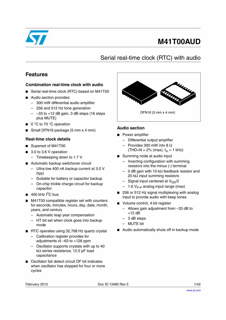
■ Small DFN16 package (5 mm x 4 mm)
Real-time clock details
■ Superset of M41T00
■ 3.0 to 3.6 V operation– Timekeeping down to 1.7 V
■ Automatic backup switchover circuit– Ultra-low 400 nA backup current at 3.0 V
(typ)– Suitable for battery or capacitor backup– On-chip trickle charge circuit for backup
capacitor
■ 400 kHz I2C bus
■ M41T00 compatible register set with counters for seconds, minutes, hours, day, date, month, years, and century– Automatic leap year compensation– HT bit set when clock goes into backup
mode
■ RTC operates using 32,768 Hz quartz crystal– Calibration register provides for
adjustments of –63 to +126 ppm– Oscillator supports crystals with up to 40
kΩ series resistance, 12.5 pF load capacitance
■ Oscillator fail detect circuit OF bit indicates when oscillator has stopped for four or more cycles
Audio section
■ Power amplifier– Differential output amplifier– Provides 300 mW into 8 Ω
(THD+N = 2% (max), fin = 1 kHz)
■ Summing node at audio input– Inverting configuration with summing
resistors into the minus (-) terminal– 0 dB gain with 10 kΩ feedback resistor and
20 kΩ input summing resistors– Signal input centered at VDD/2– 1.6 VP-P analog input range (max)
■ 256 or 512 Hz signal multiplexing with analog input to provide audio with beep tones
■ Volume control, 4-bit register– Allows gain adjustment from –33 dB to
+12 dB – 3 dB steps– MUTE bit
■ Audio automatically shuts off in backup mode
DFN16 (5 mm x 4 mm)
www.st.com
Contents M41T00AUD
2/42 Doc ID 13480 Rev 5
Contents
1 Description . . . . . . . . . . . . . . . . . . . . . . . . . . . . . . . . . . . . . . . . . . . . . . . . . 6
2 Pin settings . . . . . . . . . . . . . . . . . . . . . . . . . . . . . . . . . . . . . . . . . . . . . . . . 7
2.1 Pin connection . . . . . . . . . . . . . . . . . . . . . . . . . . . . . . . . . . . . . . . . . . . . . . 7
2.2 Pin description . . . . . . . . . . . . . . . . . . . . . . . . . . . . . . . . . . . . . . . . . . . . . . 7
3 Application . . . . . . . . . . . . . . . . . . . . . . . . . . . . . . . . . . . . . . . . . . . . . . . . . 8
4 Operation . . . . . . . . . . . . . . . . . . . . . . . . . . . . . . . . . . . . . . . . . . . . . . . . . 10
4.1 2-wire bus characteristics . . . . . . . . . . . . . . . . . . . . . . . . . . . . . . . . . . . . . 11
4.2 Characteristics . . . . . . . . . . . . . . . . . . . . . . . . . . . . . . . . . . . . . . . . . . . . . 13
4.3 READ mode . . . . . . . . . . . . . . . . . . . . . . . . . . . . . . . . . . . . . . . . . . . . . . . 13
4.4 WRITE mode . . . . . . . . . . . . . . . . . . . . . . . . . . . . . . . . . . . . . . . . . . . . . . 15
4.5 Data retention mode . . . . . . . . . . . . . . . . . . . . . . . . . . . . . . . . . . . . . . . . . 15
5 M41T00AUD clock operation . . . . . . . . . . . . . . . . . . . . . . . . . . . . . . . . . 16
5.1 Clock registers . . . . . . . . . . . . . . . . . . . . . . . . . . . . . . . . . . . . . . . . . . . . . 16
5.1.1 Halt bit operation . . . . . . . . . . . . . . . . . . . . . . . . . . . . . . . . . . . . . . . . . . 17
5.1.2 Oscillator fail detect operation . . . . . . . . . . . . . . . . . . . . . . . . . . . . . . . . 17
5.1.3 Trickle charger . . . . . . . . . . . . . . . . . . . . . . . . . . . . . . . . . . . . . . . . . . . . 17
5.2 Reading and writing the clock registers . . . . . . . . . . . . . . . . . . . . . . . . . . 18
5.3 Priority for IRQ/FT/OUT pin . . . . . . . . . . . . . . . . . . . . . . . . . . . . . . . . . . . 21
5.4 Switchover thresholds . . . . . . . . . . . . . . . . . . . . . . . . . . . . . . . . . . . . . . . 22
5.5 Trickle charge circuit . . . . . . . . . . . . . . . . . . . . . . . . . . . . . . . . . . . . . . . . . 23
6 Clock calibration . . . . . . . . . . . . . . . . . . . . . . . . . . . . . . . . . . . . . . . . . . . 24
6.1 Digital calibration (periodic counter correction) . . . . . . . . . . . . . . . . . . . . 24
7 Audio section operation . . . . . . . . . . . . . . . . . . . . . . . . . . . . . . . . . . . . . 28
7.1 Gain . . . . . . . . . . . . . . . . . . . . . . . . . . . . . . . . . . . . . . . . . . . . . . . . . . . . . 30
7.1.1 Gain tolerance . . . . . . . . . . . . . . . . . . . . . . . . . . . . . . . . . . . . . . . . . . . . 30
7.2 Wake-up time: TWU . . . . . . . . . . . . . . . . . . . . . . . . . . . . . . . . . . . . . . . . . . . . . . . . . . . . . 31
M41T00AUD Contents
Doc ID 13480 Rev 5 3/42
8 Initial conditions . . . . . . . . . . . . . . . . . . . . . . . . . . . . . . . . . . . . . . . . . . . 32
9 Maximum ratings . . . . . . . . . . . . . . . . . . . . . . . . . . . . . . . . . . . . . . . . . . . 33
10 DC and AC parameters . . . . . . . . . . . . . . . . . . . . . . . . . . . . . . . . . . . . . . 34
11 Package mechanical data . . . . . . . . . . . . . . . . . . . . . . . . . . . . . . . . . . . . 37
12 Part numbering . . . . . . . . . . . . . . . . . . . . . . . . . . . . . . . . . . . . . . . . . . . . 40
13 Revision history . . . . . . . . . . . . . . . . . . . . . . . . . . . . . . . . . . . . . . . . . . . 41
List of tables M41T00AUD
4/42 Doc ID 13480 Rev 5
List of tables
Table 1. Pin description . . . . . . . . . . . . . . . . . . . . . . . . . . . . . . . . . . . . . . . . . . . . . . . . . . . . . . . . . . . 7Table 2. List of registers . . . . . . . . . . . . . . . . . . . . . . . . . . . . . . . . . . . . . . . . . . . . . . . . . . . . . . . . . . 10Table 3. AC characteristics. . . . . . . . . . . . . . . . . . . . . . . . . . . . . . . . . . . . . . . . . . . . . . . . . . . . . . . . 13Table 4. M41T00AUD register map . . . . . . . . . . . . . . . . . . . . . . . . . . . . . . . . . . . . . . . . . . . . . . . . . 19Table 5. Priority for IRQ/FT/OUT pin . . . . . . . . . . . . . . . . . . . . . . . . . . . . . . . . . . . . . . . . . . . . . . . . 21Table 6. Digital calibration values . . . . . . . . . . . . . . . . . . . . . . . . . . . . . . . . . . . . . . . . . . . . . . . . . . . 26Table 7. MUTE and GAIN values (VCC = 3.3 V and ambient temperature = 25 °C). . . . . . . . . . . . . 29Table 8. Initial values . . . . . . . . . . . . . . . . . . . . . . . . . . . . . . . . . . . . . . . . . . . . . . . . . . . . . . . . . . . . 32Table 9. Absolute maximum ratings . . . . . . . . . . . . . . . . . . . . . . . . . . . . . . . . . . . . . . . . . . . . . . . . . 33Table 10. Operating and AC measurement conditions. . . . . . . . . . . . . . . . . . . . . . . . . . . . . . . . . . . . 34Table 11. Input/output characteristics (25 °C, f = 1 MHz) . . . . . . . . . . . . . . . . . . . . . . . . . . . . . . . . . . 34Table 12. DC characteristics. . . . . . . . . . . . . . . . . . . . . . . . . . . . . . . . . . . . . . . . . . . . . . . . . . . . . . . . 35Table 13. Crystal electrical characteristics . . . . . . . . . . . . . . . . . . . . . . . . . . . . . . . . . . . . . . . . . . . . . 35Table 14. RTC power down/up AC characteristics . . . . . . . . . . . . . . . . . . . . . . . . . . . . . . . . . . . . . . . 36Table 15. RTC power down/up trip points DC characteristics . . . . . . . . . . . . . . . . . . . . . . . . . . . . . . 36Table 16. Audio section electrical characteristics, valid for VCC = 3.3 V and
TAMB = 25 °C (except where otherwise noted) . . . . . . . . . . . . . . . . . . . . . . . . . . . . . . . . . . 36Table 17. DFN16 (5 mm x 4 mm) package mechanical data . . . . . . . . . . . . . . . . . . . . . . . . . . . . . . . 38Table 18. Ordering information scheme . . . . . . . . . . . . . . . . . . . . . . . . . . . . . . . . . . . . . . . . . . . . . . . 40Table 19. Document revision history . . . . . . . . . . . . . . . . . . . . . . . . . . . . . . . . . . . . . . . . . . . . . . . . . 41
M41T00AUD List of figures
Doc ID 13480 Rev 5 5/42
List of figures
Figure 1. Logic diagram . . . . . . . . . . . . . . . . . . . . . . . . . . . . . . . . . . . . . . . . . . . . . . . . . . . . . . . . . . . . 6Figure 2. Pin connection . . . . . . . . . . . . . . . . . . . . . . . . . . . . . . . . . . . . . . . . . . . . . . . . . . . . . . . . . . . 7Figure 3. Application diagram . . . . . . . . . . . . . . . . . . . . . . . . . . . . . . . . . . . . . . . . . . . . . . . . . . . . . . . 8Figure 4. Typical hookup example . . . . . . . . . . . . . . . . . . . . . . . . . . . . . . . . . . . . . . . . . . . . . . . . . . . . 9Figure 5. Serial bus data transfer sequence . . . . . . . . . . . . . . . . . . . . . . . . . . . . . . . . . . . . . . . . . . . 12Figure 6. Acknowledgement sequence . . . . . . . . . . . . . . . . . . . . . . . . . . . . . . . . . . . . . . . . . . . . . . . 12Figure 7. Bus timing requirements sequence . . . . . . . . . . . . . . . . . . . . . . . . . . . . . . . . . . . . . . . . . . 12Figure 8. Slave address location . . . . . . . . . . . . . . . . . . . . . . . . . . . . . . . . . . . . . . . . . . . . . . . . . . . . 14Figure 9. READ mode sequence . . . . . . . . . . . . . . . . . . . . . . . . . . . . . . . . . . . . . . . . . . . . . . . . . . . . 14Figure 10. Alternate READ mode sequence . . . . . . . . . . . . . . . . . . . . . . . . . . . . . . . . . . . . . . . . . . . . 14Figure 11. WRITE mode sequence . . . . . . . . . . . . . . . . . . . . . . . . . . . . . . . . . . . . . . . . . . . . . . . . . . . 15Figure 12. Counter update diagram . . . . . . . . . . . . . . . . . . . . . . . . . . . . . . . . . . . . . . . . . . . . . . . . . . . 20Figure 13. Switchover thresholds. . . . . . . . . . . . . . . . . . . . . . . . . . . . . . . . . . . . . . . . . . . . . . . . . . . . . 22Figure 14. Trickle charge circuit . . . . . . . . . . . . . . . . . . . . . . . . . . . . . . . . . . . . . . . . . . . . . . . . . . . . . . 23Figure 15. Crystal accuracy across temperature . . . . . . . . . . . . . . . . . . . . . . . . . . . . . . . . . . . . . . . . . 27Figure 16. Audio section diagram . . . . . . . . . . . . . . . . . . . . . . . . . . . . . . . . . . . . . . . . . . . . . . . . . . . . 28Figure 17. AC testing input/output waveform. . . . . . . . . . . . . . . . . . . . . . . . . . . . . . . . . . . . . . . . . . . . 34Figure 18. Power down/up mode AC waveforms. . . . . . . . . . . . . . . . . . . . . . . . . . . . . . . . . . . . . . . . . 36Figure 19. DFN16 (5 mm x 4 mm) package outline . . . . . . . . . . . . . . . . . . . . . . . . . . . . . . . . . . . . . . . 38Figure 20. DFN16 (5 mm x 4 mm) footprint . . . . . . . . . . . . . . . . . . . . . . . . . . . . . . . . . . . . . . . . . . . . . 39
Description M41T00AUD
6/42 Doc ID 13480 Rev 5
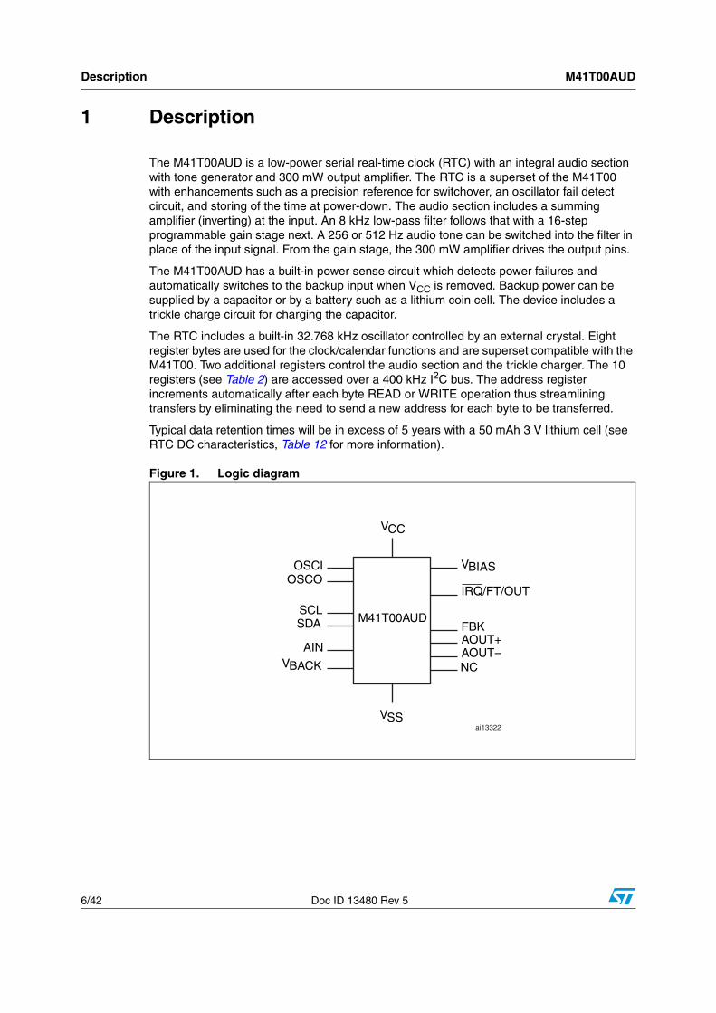
1 Description
The M41T00AUD is a low-power serial real-time clock (RTC) with an integral audio section with tone generator and 300 mW output amplifier. The RTC is a superset of the M41T00 with enhancements such as a precision reference for switchover, an oscillator fail detect circuit, and storing of the time at power-down. The audio section includes a summing amplifier (inverting) at the input. An 8 kHz low-pass filter follows that with a 16-step programmable gain stage next. A 256 or 512 Hz audio tone can be switched into the filter in place of the input signal. From the gain stage, the 300 mW amplifier drives the output pins.
The M41T00AUD has a built-in power sense circuit which detects power failures and automatically switches to the backup input when VCC is removed. Backup power can be supplied by a capacitor or by a battery such as a lithium coin cell. The device includes a trickle charge circuit for charging the capacitor.
The RTC includes a built-in 32.768 kHz oscillator controlled by an external crystal. Eight register bytes are used for the clock/calendar functions and are superset compatible with the M41T00. Two additional registers control the audio section and the trickle charger. The 10 registers (see Table 2) are accessed over a 400 kHz I2C bus. The address register increments automatically after each byte READ or WRITE operation thus streamlining transfers by eliminating the need to send a new address for each byte to be transferred.
Typical data retention times will be in excess of 5 years with a 50 mAh 3 V lithium cell (see RTC DC characteristics, Table 12 for more information).
Figure 1. Logic diagram
OSCI
VCC
M41T00AUD
VSS
SCL
OSCOIRQ/FT/OUT
SDA
VBIAS
AINVBACK
AOUT+AOUT –NC
FBK
ai13322
M41T00AUD Pin settings
Doc ID 13480 Rev 5 7/42
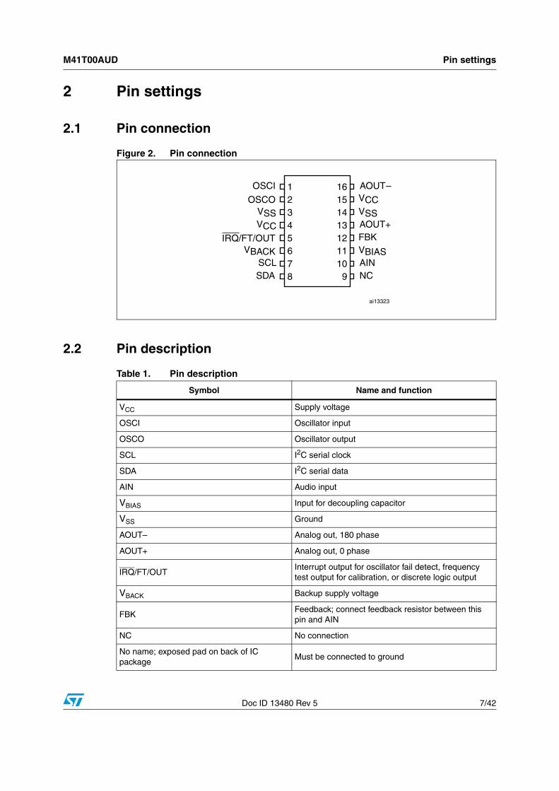
2 Pin settings
2.1 Pin connection
Figure 2. Pin connection
2.2 Pin description
OSCI 1OSCO 2
VSS 34VCC
IRQ/FT/OUTVBACK
SCLSDA
5678
16151413121110
9
VCC
AOUT+FBKVBIAS
NC
AOUT–
AIN
VSS
ai13323
Table 1. Pin description
Symbol Name and function
VCC Supply voltage
OSCI Oscillator input
OSCO Oscillator output
SCL I2C serial clock
SDA I2C serial data
AIN Audio input
VBIAS Input for decoupling capacitor
VSS Ground
AOUT– Analog out, 180 phase
AOUT+ Analog out, 0 phase
IRQ/FT/OUTInterrupt output for oscillator fail detect, frequency test output for calibration, or discrete logic output
VBACK Backup supply voltage
FBKFeedback; connect feedback resistor between this pin and AIN
NC No connection
No name; exposed pad on back of IC package
Must be connected to ground
Application M41T00AUD
8/42 Doc ID 13480 Rev 5
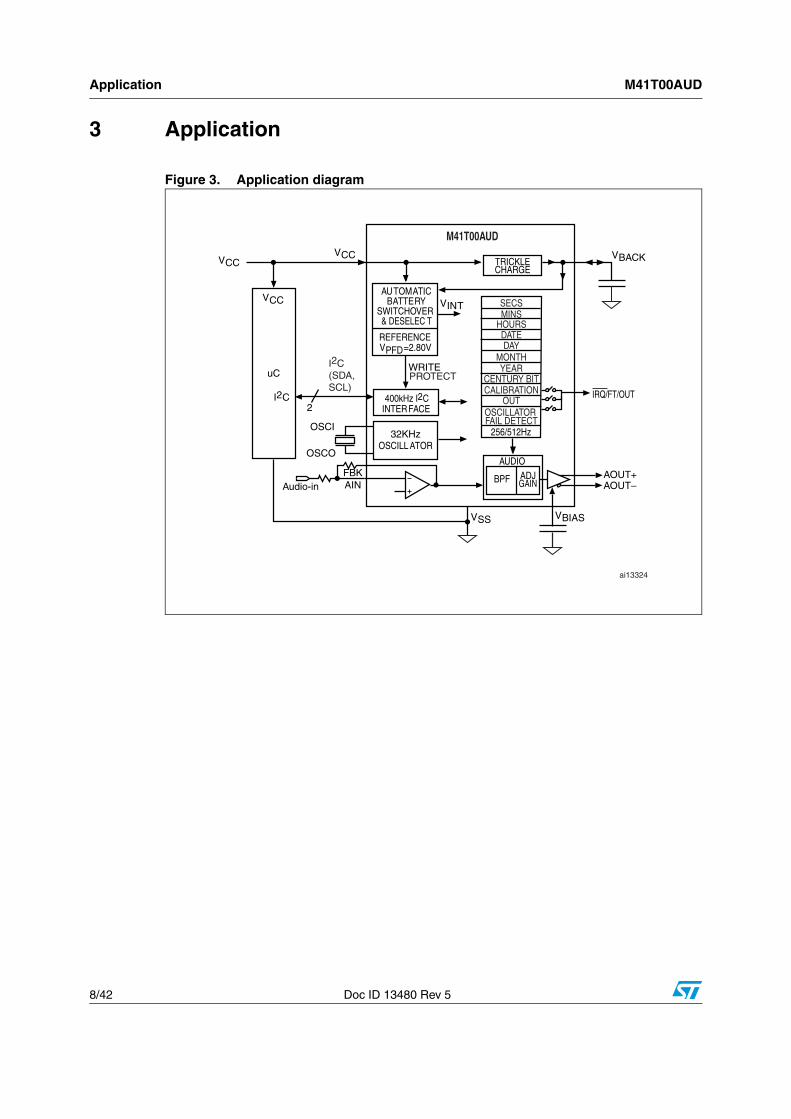
3 Application
Figure 3. Application diagram
AUTOMATICBATTERY
SWITCHOVER& DESELEC T
VCC
2I2C
VCC
32KHzOSCILL ATOR
400kHz I2CINTERFACE
OSCI
OSCO
uC
REFERENCEVPFD=2.80V
IRQ/FT/OUT
TRICKLECHARGE
VINT
VBACKVCC
256/512Hz
AUDIO
BPF ADJGAINAIN
AOUT+AOUT–
VSS VBIAS
WRITE
FBKAudio-in
M41T00AUD
ai13324
SECSMINS
HOURSDATEDAY
MONTHYEAR
CENTURY BITCALIBRATION
OUTOSCILLATOR FAIL DETECT
I2C(SDA, SCL)
PROTECT
M41T00AUD Application
Doc ID 13480 Rev 5 9/42
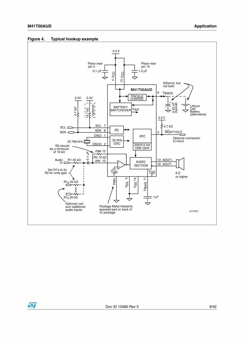
Figure 4. Typical hookup example
BATTERYSWITCHOVER
32 KHzOSC
I2C
OSCI
OSCO
IRQ/FT/OUT
TRICKLECHARGE
VINT
VBACK
256/512 Hz
AUDIO SECTION
AIN AOUT+AOUT–
VB
IAS
0.1
µF
AudioIn
0.22
µF
3.3 V
0.1 µF
VC
C 1.0 µF
VC
C
4 15SCL 7
SDA 8
3.3V
SCL
SDA
3.3V
1
232.768 kHz
6
+
(typ
ical
)
Lithium Cell Battery(alternative)
Either/or, butnot both
5
Optional connectionto micro
1316
11
R1x
R1x
Optional: cansum additionalaudio inputs
Set R1’s to 2x R2 for unity gain
10
PM
H
Package Metal Heatsink:exposed pad on back of IC package
RTC
*opt
iona
l
VS
S3
VS
S14
Place near pin 15
Place near pin 4
VDD2
VDD2
FBK 12
3.3 V
R2 shouldbe a minimum ONE GEN
M41T00AUD
ai13325
Operation M41T00AUD
10/42 Doc ID 13480 Rev 5
4 Operation
The M41T00AUD clock operates as a slave device on the serial bus. Access is obtained by implementing a start condition followed by the correct slave address (D0h). The 10 bytes contained in the device can then be accessed sequentially in the following order:
The M41T00AUD continually monitors VCC for an out of tolerance condition. Should VCC fall below VPFD, the device terminates an access in progress and resets the device address counter. Inputs to the device will not be recognized at this time to prevent erroneous data from being written to the device from an out of tolerance system. When VCC falls below VSO, the device automatically switches over to the backup battery or capacitor and powers down into an ultra low current mode of operation to conserve battery life. Upon power-up, the device switches from battery to VCC at VSO and recognizes inputs.
Table 2. List of registers
Byte address Contents
00h Seconds register
01h Minutes register
02h Century/hours register
03h Day register
04h Date register
05h Month register
06h Years register
07h Calibration/control register
08h Audio register
09h Control2 register
M41T00AUD Operation
Doc ID 13480 Rev 5 11/42
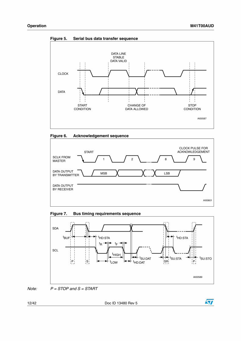
4.1 2-wire bus characteristicsThis bus is intended for communication between different ICs. It consists of two lines: one bi-directional for data signals (SDA) and one for clock signals (SCL). Both the SDA and the SCL lines must be connected to a positive supply voltage via a pull-up resistor.
The following protocol has been defined:
● Data transfer may be initiated only when the bus is not busy.
● During data transfer, the data line must remain stable whenever the clock line is high. Changes in the data line while the clock line is high will be interpreted as control signals.
Accordingly, the following bus conditions have been defined:
● Bus not busy. Both data and clock lines remain high.
● Start data transfer. A change in the state of the data line, from high to low, while the clock is high, defines the START condition.
● Stop data transfer. A change in the state of the data line, from low to high, while the clock is high, defines the STOP condition.
● Data valid. The state of the data line represents valid data when after a start condition, the data line is stable for the duration of the high period of the clock signal. The data on the line may be changed during the low period of the clock signal. There is one clock pulse per bit of data.
Each data transfer is initiated with a start condition and terminated with a stop condition. The number of data bytes transferred between the start and stop conditions is not limited. The information is transmitted byte-wide and each receiver acknowledges with a ninth bit. By definition, a device that gives out a message is called "transmitter", the receiving device that gets the message is called "receiver". The device that controls the message is called "master". The devices that are controlled by the master are called "slaves".
● Acknowledge. Each byte of eight bits is followed by one acknowledge bit. This acknowledge bit is a low level put on the bus by the receiver, whereas the master generates an extra acknowledge related clock pulse.
A slave receiver which is addressed is obliged to generate an acknowledge after the reception of each byte. Also, a master receiver must generate an acknowledge after the reception of each byte that has been clocked out of the slave transmitter.
The device that acknowledges has to pull down the SDA line during the acknowledge clock pulse in such a way that the SDA line is a stable Low during the high period of the acknowledge related clock pulse. Of course, setup and hold times must be taken into account. A master receiver must signal an end-of-data to the slave transmitter by not generating an acknowledge on the last byte that has been clocked out of the slave. In this case, the transmitter must leave the data line high to enable the master to generate the STOP condition.
Operation M41T00AUD
12/42 Doc ID 13480 Rev 5
Figure 5. Serial bus data transfer sequence
Figure 6. Acknowledgement sequence
Figure 7. Bus timing requirements sequence
Note: P = STOP and S = START
AI00587
DATA
CLOCK
DATA LINESTABLE
DATA VALID
STARTCONDITION
CHANGE OFDATA ALLOWED
STOPCONDITION
AI00601
DATA OUTPUTBY RECEIVER
DATA OUTPUTBY TRANSMITTER
SCLK FROMMASTER
STARTCLOCK PULSE FOR
ACKNOWLEDGEMENT
1 2 8 9
MSB LSB
AI00589
SDA
PtSU:STOtSU:STA
tHD:STA
SR
SCL
tSU:DAT
tF
tHD:DAT
tR
tHIGH
tLOW
tHD:STAtBUF
SP
M41T00AUD Operation
Doc ID 13480 Rev 5 13/42
4.2 Characteristics
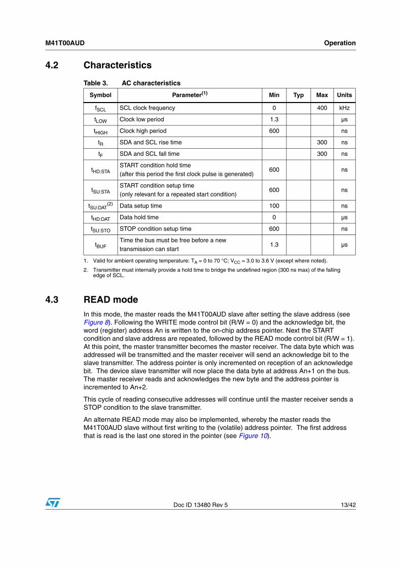
4.3 READ modeIn this mode, the master reads the M41T00AUD slave after setting the slave address (see Figure 8). Following the WRITE mode control bit (R/W = 0) and the acknowledge bit, the word (register) address An is written to the on-chip address pointer. Next the START condition and slave address are repeated, followed by the READ mode control bit (R/W = 1). At this point, the master transmitter becomes the master receiver. The data byte which was addressed will be transmitted and the master receiver will send an acknowledge bit to the slave transmitter. The address pointer is only incremented on reception of an acknowledge bit. The device slave transmitter will now place the data byte at address An+1 on the bus. The master receiver reads and acknowledges the new byte and the address pointer is incremented to An+2.
This cycle of reading consecutive addresses will continue until the master receiver sends a STOP condition to the slave transmitter.
An alternate READ mode may also be implemented, whereby the master reads the M41T00AUD slave without first writing to the (volatile) address pointer. The first address that is read is the last one stored in the pointer (see Figure 10).
Table 3. AC characteristics
Symbol Parameter(1)
1. Valid for ambient operating temperature: TA = 0 to 70 °C; VCC = 3.0 to 3.6 V (except where noted).
Min Typ Max Units
fSCL SCL clock frequency 0 400 kHz
tLOW Clock low period 1.3 µs
tHIGH Clock high period 600 ns
tR SDA and SCL rise time 300 ns
tF SDA and SCL fall time 300 ns
tHD:STASTART condition hold time(after this period the first clock pulse is generated)
600 ns
tSU:STASTART condition setup time(only relevant for a repeated start condition)
600 ns
tSU:DAT(2)
2. Transmitter must internally provide a hold time to bridge the undefined region (300 ns max) of the falling edge of SCL.
Data setup time 100 ns
tHD:DAT Data hold time 0 µs
tSU:STO STOP condition setup time 600 ns
tBUFTime the bus must be free before a new
transmission can start1.3 µs
Operation M41T00AUD
14/42 Doc ID 13480 Rev 5
Figure 8. Slave address location
Figure 9. READ mode sequence
Figure 10. Alternate READ mode sequence
AI00602
R/W
SLAVE ADDRESSSTART A
0 1 0 0 01 1
MS
B
LSB
AI00899
BUS ACTIVITY:
AC
K
S
AC
K
AC
K
AC
K
NO
AC
KS
TOP
STA
RT
P
SDA LINE
BUS ACTIVITY:MASTER R
/W
DATA n DATA n+1
DATA n+X
WORDADDRESS (An)
SLAVEADDRESS
S
STA
RT
R/W
SLAVEADDRESS
AC
K
AI00895
BUS ACTIVITY:
AC
K
S
AC
K
AC
K
AC
K
N
O A
CK
STO
P
STA
RT
PSDA LINE
BUS ACTIVITY:MASTER R
/W
DATA n DATA n+1 DATA n+X
SLAVEADDRESS
M41T00AUD Operation
Doc ID 13480 Rev 5 15/42
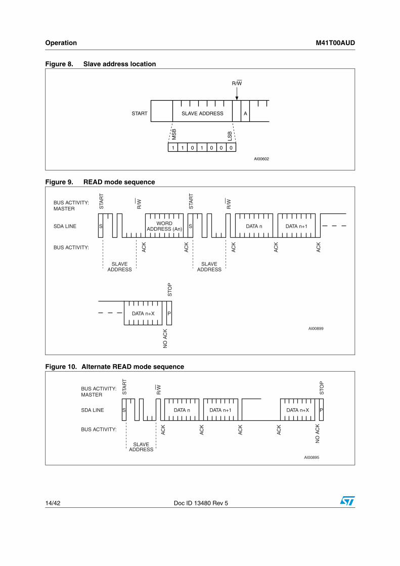
4.4 WRITE modeIn this mode the master transmitter transmits to the M41T00AUD slave receiver. Bus protocol is shown in Figure 11. Following the START condition and slave address, a logic '0' (R/W = 0) is placed on the bus and indicates to the addressed device that word address An will follow and is to be written to the on-chip address pointer. The data word to be written to the device is strobed in next and the internal address pointer is incremented to the next location within the device on the reception of an acknowledge clock. The M41T00AUD slave receiver will send an acknowledge clock to the master transmitter after it has received the slave address and again after it has received the word address and each data byte (see Figure 8).
Figure 11. WRITE mode sequence
4.5 Data retention modeWith valid VCC applied, the M41T00AUD can be accessed as described above with READ or WRITE cycles. Should the supply voltage decay, the M41T00AUD will automatically deselect, write protecting itself when VCC falls (see Figure 13).
AI00591
BUS ACTIVITY:
AC
K
S
AC
K
AC
K
AC
K
AC
KS
TOP
STA
RT
PSDA LINE
BUS ACTIVITY:MASTER R
/W
DATA n DATA n+1 DATA n+XWORDADDRESS (An)
SLAVEADDRESS
M41T00AUD clock operation M41T00AUD
16/42 Doc ID 13480 Rev 5
5 M41T00AUD clock operation
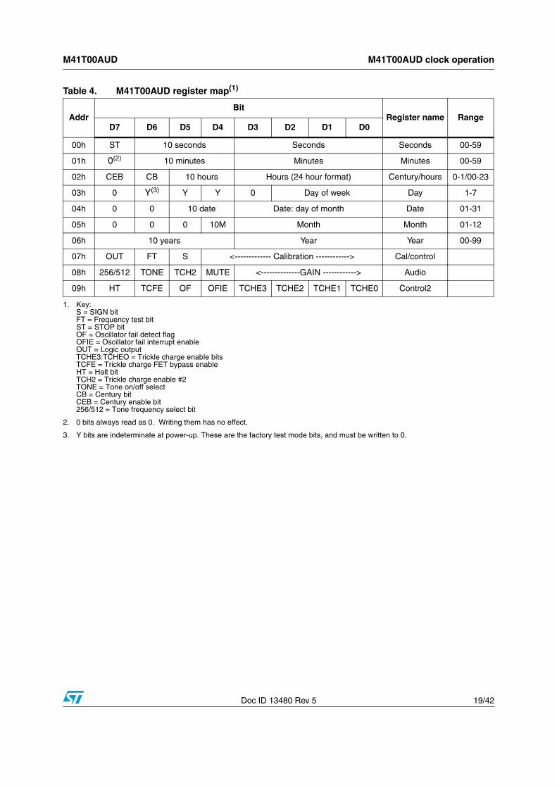
5.1 Clock registersThe 10-byte register map (see Table 2) is used to both set the clock and to read the date and time from the clock, in a binary coded decimal format.
Seconds, minutes, and hours are contained within the first three registers. Bits D6 to D0 or register 00h (seconds register) contain the seconds count in BCD format with values in the range 0 to 59. Bit D7 is the ST or stop bit, described below, and is not affected by the timekeeping operation, but users must avoid inadvertently altering it when writing the seconds register.
Setting the ST bit to a 1 will cause the oscillator to stop. If the device is expected to spend a significant amount of time on the shelf, the oscillator may be stopped to reduce current drain on the backup battery. When reset to a 0 the oscillator restarts within one second.
In order to ensure oscillator start-up after the initial power-up, set the ST bit to a 1 then write it to 0. This sequence enables the "kick start" circuit which aids the oscillator start-up by temporarily increasing the oscillator current. This will guarantee oscillator start-up under worst case conditions of voltage and temperature. This feature can be employed anytime the oscillator is being started but should not occur on subsequent power-ups when the oscillator is already running.
Bits D6 to D0 of register 01h (minutes register) contain the minutes count in BCD format with values in the range 0 to 59. Bit D7 always reads 0. Writing it has no effect.
Bits D5 to D0 of register 02h (century/ hours register) contain the hours in BCD format with values in the range 0 to 23. Bits D7 and D6 contain the century enable bit (CEB) and the century bit (CB). CB provides a one-bit indicator for the century. The user can apply his preferred convention for defining the meaning of this bit. For example, 0 can mean the current century, and 1 the next, or the opposite meanings may be used.
When enabled, CB will toggle every 100 years. Setting CEB to a 1 enables CB to toggle at the turn of the century, either from 0 to 1 or from 1 to 0, depending on its initial state, as programmed by the user. When CEB is a 0, CB will not toggle.
Bits D2 through D0 of register 03h (day register) contain the day of the week in BCD format with values in the range 0 to 7. Bits D3 and D7 will always read 0. Writes to them have no effect. Bits D6, D5 and D4 will power up in an indeterminate state.
Register 04h contains the date (day of month) in BCD format with values in the range 01 to 31. Bits D7 and D6 always read 0. Writes to them have no effect.
Register 05 h is the Month in BCD format with values in the range 1 to 12. Bits D7, D6 and D5 always read 0. Writes to them have no effect.
Register 06h is the years in BCD format with values in the range 0 to 99. Writing to any of the registers 00h to 06h, including the control bits therein, will result in updates to the counters and resetting of the internal clock divider chain including the 256/512 Hz tone generator. The updates do not occur immediately after the write(s), but occur upon completion of the current write access. This is described in greater detail in the next section.
Registers 07h and 09h also contain clock control and status information. These registers can be written at any time without affecting the timekeeping function.
M41T00AUD M41T00AUD clock operation
Doc ID 13480 Rev 5 17/42
Register 08 is the calibration register. Calibration is described in detail in the clock calibration section. Bit D7 is the OUT bit and controls the discrete output pin IRQ/FT/OUT as described in Table 5.
5.1.1 Halt bit operation
Bit D7 of register 09 h is the HT or halt bit. Whenever the device switches to backup power, it sets the HT bit to 1 and stores the time of power-down in the transfer buffer registers. This is known as power-down time stamp. During normal timekeeping, once per second, the transfer buffer registers are updated with the current time. When HT is 1, that updating is halted. The clock continues to keep time but the periodic updates do not occur.
Upon power-up, reads of the clock registers will return the time of power-down (assuming adequate backup power was maintained while VCC was off). After the user clears the HT bit by writing it to 0, subsequent reads of the clock registers will return the current time.
At power-up, the user can read the time of power-down, and then clear the HT bit to allow updates. The next read will return the current time. Knowing both the power-up time and the power-down time allows the user to calculate the duration of power-off.
In addition to the HT bit getting set to 1 automatically at power-down, the user can also write it to 1 to halt updating of the registers.
5.1.2 Oscillator fail detect operation
Bits D5 and D4 of register 09 h contain the oscillator fail flag (OF) and the oscillator fail interrupt enable bit (OFIE). If the 32 KHz oscillator drops four or more pulses in a row, as might occur during an extended outage while backed up on a capacitor, the OF bit will be set to 1. This provides an indication to the user of the integrity of the timekeeping operation. Whenever the OF bit is a 1, the system should consider the time to be possibly corrupted due to operating at too low a voltage. The OF bit will always be 1 at the initial power-up of the device. The OF bit is cleared by writing it to 0. At the initial power-up, users should wait three seconds for the oscillator to stabilize before clearing the OF bit.
OFIE can be used to enable the device to assert its interrupt output whenever an oscillator failure is detected. The oscillator fail interrupt will drive the IRQ/FT/OUT pin as described in Table 5. The interrupt is cleared by writing the OF bit to 0. Setting OFIE enables the oscillator fail interrupt. Clearing it to 0 disables it, but the OF will continue to function regardless of OFIE.
5.1.3 Trickle charger
Bits D6 and D3 to D0, of register 09h, control the trickle charge function. It is described in detail in the trickle charge circuit section.
M41T00AUD clock operation M41T00AUD
18/42 Doc ID 13480 Rev 5
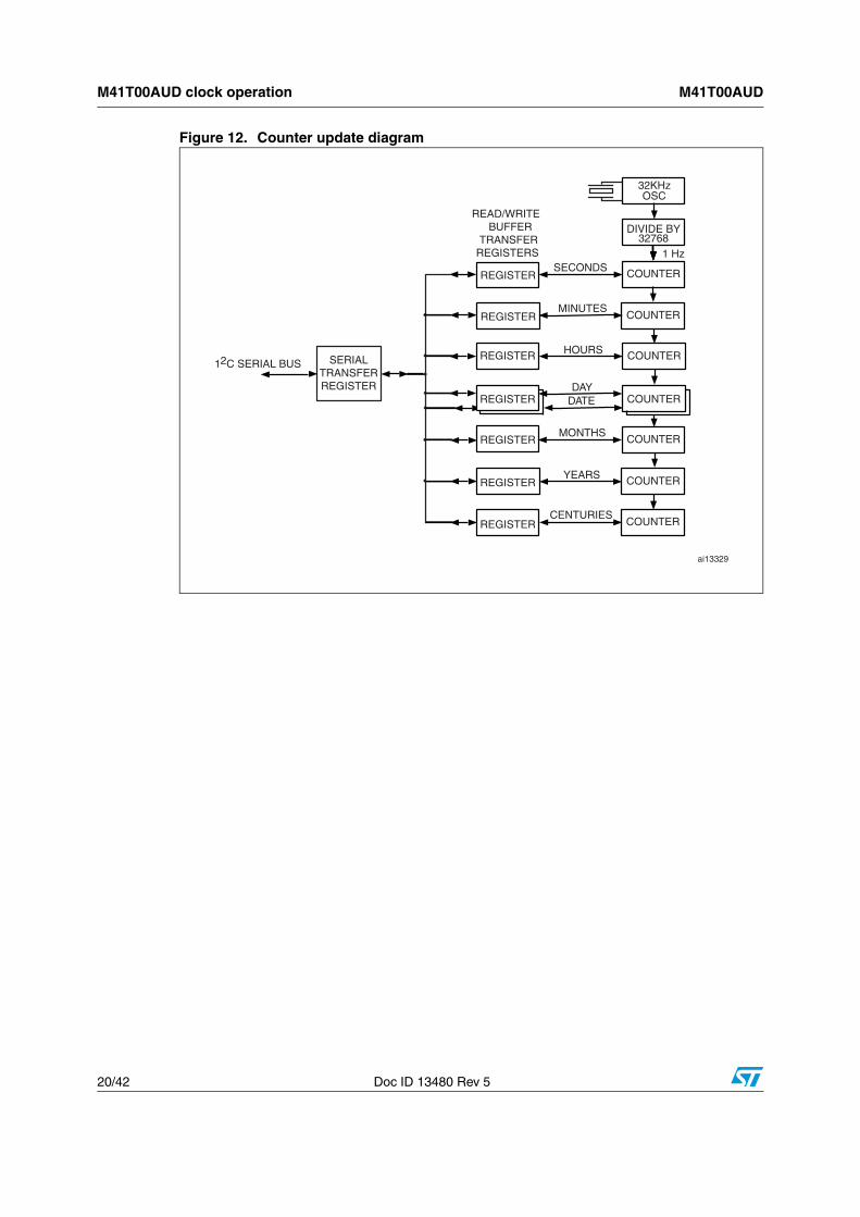
5.2 Reading and writing the clock registersThe counters used to implement the timing chain in the real-time clock are not directly accessed by the serial interface. Instead, as depicted in Figure 12, reads and writes are buffered through a set of transfer registers. This ensures coherency of the timekeeping function.
During writes of the timekeeping registers (00h to 06h), the write data is stored in the buffer transfer registers until all the data is written, then the register contents are simultaneously transferred to the counters thus updating them. The update is triggered either by a STOP condition or by a write to one of the non RTC registers, 07h to 09h. If any of the buffer transfer registers are not written, then the corresponding counters are not updated. Instead, those counters will retain their previous contents when the update occurs.
Similar to the writes, reads access the buffer transfer registers. The device periodically updates the registers with the counter contents. But during reads, the updates are suspended. Timekeeping continues, but the registers are frozen until after a STOP condition or a non RTC register (07h to 09h) is read. Suspending the updates ensures that a clock roll-over does not occur during a user read cycle.
The seven clock registers may be read one byte at a time, or in a sequential block. The calibration, audio and Control2 registers, location 07 h to 09 h, may be accessed independently.
Provision has been made to ensure that a clock update does not occur while any of the seven clock addresses are being read. During a clock register read (addresses 00h to 06h), updates of the clock transfer buffer registers are halted. The clock counters continue to keep time, but the contents of the transfer buffer registers is frozen at the time that the read access began.
This prevents a transition of data during the READ. For example, without the halt function, if the time incremented past midnight in the middle of an access sequence, the user might begin reading at 11:59:59pm and finish at 12:00:00am. The data read might appear as 12:59:59 because the seconds and minutes were read before midnight while the hours were read after. The device prevents this by halting the updates of the registers until after the read access has occurred.
M41T00AUD M41T00AUD clock operation
Doc ID 13480 Rev 5 19/42
Table 4. M41T00AUD register map(1)
AddrBit
Register name RangeD7 D6 D5 D4 D3 D2 D1 D0
00h ST 10 seconds Seconds Seconds 00-59
01h 0(2) 10 minutes Minutes Minutes 00-59
02h CEB CB 10 hours Hours (24 hour format) Century/hours 0-1/00-23
03h 0 Y(3) Y Y 0 Day of week Day 1-7
04h 0 0 10 date Date: day of month Date 01-31
05h 0 0 0 10M Month Month 01-12
06h 10 years Year Year 00-99
07h OUT FT S <------------- Calibration ------------> Cal/control
08h 256/512 TONE TCH2 MUTE <--------------GAIN ------------> Audio
09h HT TCFE OF OFIE TCHE3 TCHE2 TCHE1 TCHE0 Control2
1. Key:S = SIGN bitFT = Frequency test bitST = STOP bitOF = Oscillator fail detect flagOFIE = Oscillator fail interrupt enableOUT = Logic outputTCHE3:TCHEO = Trickle charge enable bitsTCFE = Trickle charge FET bypass enableHT = Halt bitTCH2 = Trickle charge enable #2TONE = Tone on/off selectCB = Century bitCEB = Century enable bit256/512 = Tone frequency select bit
2. 0 bits always read as 0. Writing them has no effect.
3. Y bits are indeterminate at power-up. These are the factory test mode bits, and must be written to 0.
M41T00AUD clock operation M41T00AUD
20/42 Doc ID 13480 Rev 5
Figure 12. Counter update diagram
32KHz
COUNTER
DIVIDE BY
1 HzSECONDS
MINUTES
HOURS
MONTHS
YEARS
CENTURIES
COUNTER
COUNTER
COUNTER
COUNTER
COUNTER
COUNTER
REGISTER
REGISTER
REGISTER
REGISTERDAY
DATE
REGISTER
REGISTER
REGISTER
READ/WRITE BUFFER
TRANSFER REGISTERS
SERIALTRANSFERREGISTER
ai13329
12C SERIAL BUS
32768
OSC
M41T00AUD M41T00AUD clock operation
Doc ID 13480 Rev 5 21/42
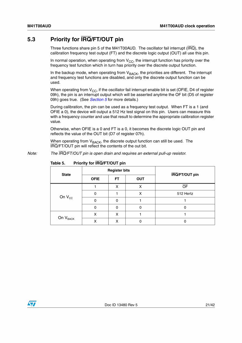
5.3 Priority for IRQ/FT/OUT pinThree functions share pin 5 of the M41T00AUD. The oscillator fail interrupt (IRQ), the calibration frequency test output (FT) and the discrete logic output (OUT) all use this pin.
In normal operation, when operating from VCC, the interrupt function has priority over the frequency test function which in turn has priority over the discrete output function.
In the backup mode, when operating from VBACK, the priorities are different. The interrupt and frequency test functions are disabled, and only the discrete output function can be used.
When operating from VCC, if the oscillator fail interrupt enable bit is set (OFIE, D4 of register 09h), the pin is an interrupt output which will be asserted anytime the OF bit (D5 of register 09h) goes true. (See Section 5 for more details.)
During calibration, the pin can be used as a frequency test output. When FT is a 1 (and OFIE a 0), the device will output a 512 Hz test signal on this pin. Users can measure this with a frequency counter and use that result to determine the appropriate calibration register value.
Otherwise, when OFIE is a 0 and FT is a 0, it becomes the discrete logic OUT pin and reflects the value of the OUT bit (D7 of register 07h).
When operating from VBACK, the discrete output function can still be used. The IRQ/FT/OUT pin will reflect the contents of the out bit.
Note: The IRQ/FT/OUT pin is open drain and requires an external pull-up resistor.
Table 5. Priority for IRQ/FT/OUT pin
StateRegister bits
IRQ/FT/OUT pinOFIE FT OUT
On VCC
1 X X OF
0 1 X 512 Hertz
0 0 1 1
0 0 0 0
On VBACK
X X 1 1
X X 0 0
M41T00AUD clock operation M41T00AUD
22/42 Doc ID 13480 Rev 5
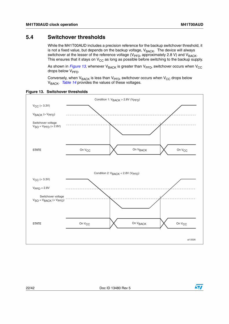
5.4 Switchover thresholdsWhile the M41T00AUD includes a precision reference for the backup switchover threshold, it is not a fixed value, but depends on the backup voltage, VBACK. The device will always switchover at the lesser of the reference voltage (VPFD, approximately 2.8 V) and VBACK. This ensures that it stays on VCC as long as possible before switching to the backup supply.
As shown in Figure 13, whenever VBACK is greater than VPFD, switchover occurs when VCC drops below VPFD.
Conversely, when VBACK is less than VPFD, switchover occurs when VCC drops below VBACK. Table 14 provides the values of these voltages.
Figure 13. Switchover thresholds
STATE On VCC On VBACK On VCC
Switchover voltageVSO = VBACK (< VPFD)
VPFD = 2.8V
VCC (= 3.3V)
Condition 2: VBACK < 2.8V (VPFD)
STATE On VCC On VBACK On VCC
Switchover voltageVSO = VPFD (= 2.8V)
VBACK (> VPFD)
VCC (= 3.3V)
Condition 1: VBACK > 2.8V (VPFD)
ai13326
M41T00AUD M41T00AUD clock operation
Doc ID 13480 Rev 5 23/42
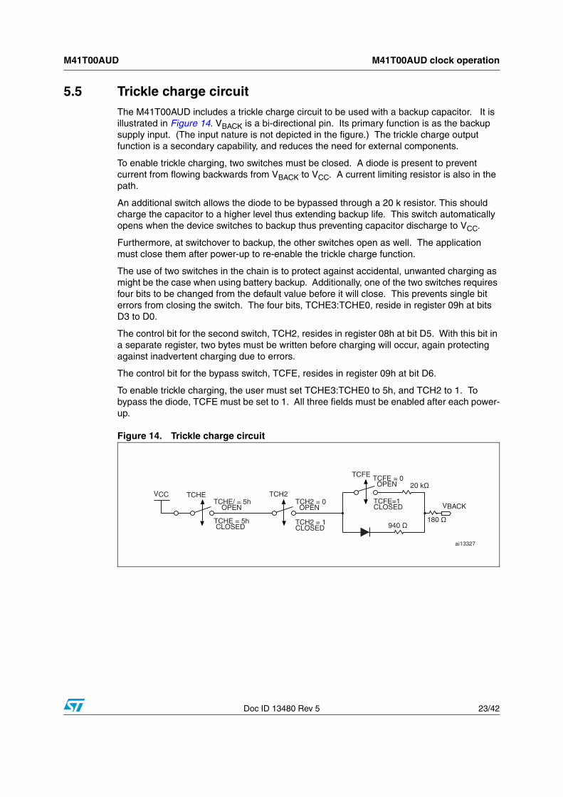
5.5 Trickle charge circuitThe M41T00AUD includes a trickle charge circuit to be used with a backup capacitor. It is illustrated in Figure 14. VBACK is a bi-directional pin. Its primary function is as the backup supply input. (The input nature is not depicted in the figure.) The trickle charge output function is a secondary capability, and reduces the need for external components.
To enable trickle charging, two switches must be closed. A diode is present to prevent current from flowing backwards from VBACK to VCC. A current limiting resistor is also in the path.
An additional switch allows the diode to be bypassed through a 20 k resistor. This should charge the capacitor to a higher level thus extending backup life. This switch automatically opens when the device switches to backup thus preventing capacitor discharge to VCC.
Furthermore, at switchover to backup, the other switches open as well. The application must close them after power-up to re-enable the trickle charge function.
The use of two switches in the chain is to protect against accidental, unwanted charging as might be the case when using battery backup. Additionally, one of the two switches requires four bits to be changed from the default value before it will close. This prevents single bit errors from closing the switch. The four bits, TCHE3:TCHE0, reside in register 09h at bits D3 to D0.
The control bit for the second switch, TCH2, resides in register 08h at bit D5. With this bit in a separate register, two bytes must be written before charging will occur, again protecting against inadvertent charging due to errors.
The control bit for the bypass switch, TCFE, resides in register 09h at bit D6.
To enable trickle charging, the user must set TCHE3:TCHE0 to 5h, and TCH2 to 1. To bypass the diode, TCFE must be set to 1. All three fields must be enabled after each power-up.
Figure 14. Trickle charge circuit
TCHEVCCTCHE/ = 5h OPEN
TCHE = 5h CLOSED
VBACK
TCH2TCH2 = 0 OPEN
TCH2 = 1CLOSED
TCFE TCFE = 0 OPEN
TCFE=1CLOSED
ai13327
Clock calibration M41T00AUD
24/42 Doc ID 13480 Rev 5
6 Clock calibration
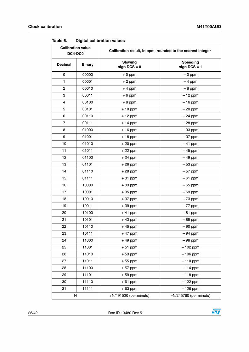
The M41T00AUD oscillator is designed for use with a 12.5 pF crystal load capacitance. With a nominal ±20 ppm crystal, the M41T00AUD will be accurate to ±35 ppm. When the calibration circuit is properly employed, accuracy improves to better than ±2 ppm at 25 °C.
The M41T00AUD design provides the following method for clock error correction.
6.1 Digital calibration (periodic counter correction)This method employs the use of periodic counter correction by adjusting the number of cycles of the internal 512 Hz signal counted in a second. By adding an extra cycle, for 513, a long second is counted for slowing the clock. By reducing it to 511 cycles, a short second is counted for speeding up the clock.
Not every second is affected. The calibration value (bits D4-D0 of register 07h) and its sign bit (D5 of same register) control how often a short or long second is generated.
The basic nature of a 32 KHz crystal is to slow down at temperatures above and below 25 °C. Whether the temperature is above or below 25 °C, the device will tend to run slow. Therefore, most corrections will need to speed the clock up. Hence, the M41T00AUD calibration circuit uses a non-symmetric calibration scheme. Positive values, for speeding the clock up, have more effect than negative values, for slowing it down. A positive value will speed the clock up by approximately 4 ppm per step. A negative value will slow it by approximately 2 ppm per step.
In the M41T00AUD's calibration circuit, positive correction is applied every 8th minute whereas negative correction is applied every 16th minute. Because positive correction is applied twice as often, it has twice the effect for a given calibration number, N. When the calibration sign bit is positive, N seconds of every 8th minute will be shortened to 511 cycles of the 512 Hz clock. When the calibration sign bit is negative, N seconds of every 16th minute will be lengthened to 513 cycles of the 512 Hz clock.
When N is positive, one minute will have N seconds which are 511 cycles and the remaining seconds will be 512 cycles. The next seven minutes are nominal with all seconds 512 cycles each.
Example 1:
Sign is 1 and N is 2 (00010b)
The 8-minute interval will be:
2 * 511 + (60-2) * 512 + 7 * 60 * 512 = 245758 cycles long out of a possible
512 * 60 * 8 = 245760 cycles of the 512 Hz clock in an 8-minute span.
This gives a net correction of (245760-245758) / 245760 = -8.138 ppm
When N is negative, one minute will have N seconds which are 513 cycles and the remaining seconds will be 512 cycles. The next 15 minutes are nominal with all seconds 512 cycles each.
M41T00AUD Clock calibration
Doc ID 13480 Rev 5 25/42
Example 2:
Sign is 0 and N is 3 (00010b). The 16-minute interval will be:
3 * 513 + (60-3) * 512 + 15 * 60 * 512 = 491523 cycles long out of a possible
512 * 60 * 16 = 491520 cycles of the 512 Hz clock in an 16-minute span.
This gives a net correction of (491520-491523) / 491520 = +6.104 ppm
Therefore, each calibration step has an effect on clock accuracy of either -4.068 or +2.034 ppm. Assuming that the oscillator is running at exactly 32,768 Hz, each of the 31 steps in the calibration byte would represent subtracting 10.7 or adding 5.35 seconds per month, which corresponds to a total range of –5.5 or +2.75 minutes per month.
Note: The modified pulses are not observable on the frequency test (FT) output, nor will the effect of the calibration be measurable real-time, due to the periodic nature of the error compensation.
Clock calibration M41T00AUD
26/42 Doc ID 13480 Rev 5
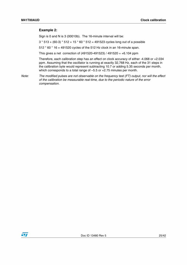
Table 6. Digital calibration values
Calibration value
DC4-DC0Calibration result, in ppm, rounded to the nearest integer
Decimal BinarySlowing
sign DCS = 0Speeding
sign DCS = 1
0 00000 + 0 ppm – 0 ppm
1 00001 + 2 ppm – 4 ppm
2 00010 + 4 ppm – 8 ppm
3 00011 + 6 ppm – 12 ppm
4 00100 + 8 ppm – 16 ppm
5 00101 + 10 ppm – 20 ppm
6 00110 + 12 ppm – 24 ppm
7 00111 + 14 ppm – 28 ppm
8 01000 + 16 ppm – 33 ppm
9 01001 + 18 ppm – 37 ppm
10 01010 + 20 ppm – 41 ppm
11 01011 + 22 ppm – 45 ppm
12 01100 + 24 ppm – 49 ppm
13 01101 + 26 ppm – 53 ppm
14 01110 + 28 ppm – 57 ppm
15 01111 + 31 ppm – 61 ppm
16 10000 + 33 ppm – 65 ppm
17 10001 + 35 ppm – 69 ppm
18 10010 + 37 ppm – 73 ppm
19 10011 + 39 ppm – 77 ppm
20 10100 + 41 ppm – 81 ppm
21 10101 + 43 ppm – 85 ppm
22 10110 + 45 ppm – 90 ppm
23 10111 + 47 ppm – 94 ppm
24 11000 + 49 ppm – 98 ppm
25 11001 + 51 ppm – 102 ppm
26 11010 + 53 ppm – 106 ppm
27 11011 + 55 ppm – 110 ppm
28 11100 + 57 ppm – 114 ppm
29 11101 + 59 ppm – 118 ppm
30 11110 + 61 ppm – 122 ppm
31 11111 + 63 ppm – 126 ppm
N +N/491520 (per minute) –N/245760 (per minute)
M41T00AUD Clock calibration
Doc ID 13480 Rev 5 27/42
Figure 15. Crystal accuracy across temperature
AI00999b
–160
0 10 20 30 40 50 60 70
Frequency (ppm)
Temperature °C
80–10–20–30–40
–100
–120
–140
–40
–60
–80
20
0
–20
DF= K x (T –TO)2
K = –0.036 ppm/˚C2 ± 0.006 ppm/˚C2
TO = 25˚C ± 5˚C
F
Audio section operation M41T00AUD
28/42 Doc ID 13480 Rev 5
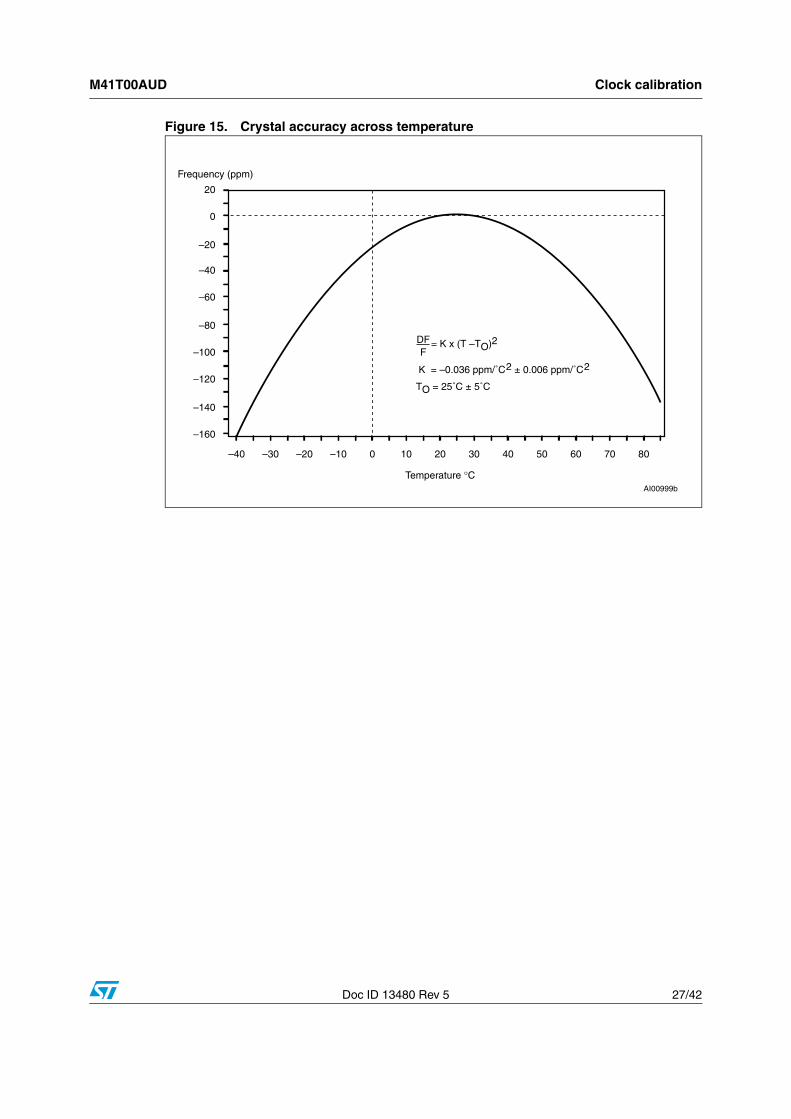
7 Audio section operation
The audio section is comprised of five main parts. The input includes a summing amplifier. A minimum 10 kΩ feedback resistor is required. With that and 20 kΩ input resistors, the input signals will be summed at unity gain.
An audio switch follows the amplifier. A tone, selectable between 256 and 512 Hz, can be inserted into the audio stream in lieu of the input amplifier's output.
A low pass filter is next with a cut off of 8 kHz. To get a band pass with a 100 Hz low end, the user should place an appropriate coupling capacitor at the input pin.
Figure 16. Audio section diagram
BPF
100 Hz - 8 kHz
256 Hz
512 Hz
256/512SELECT
TONEON/OFF
From internal RTC timing chain
register bits
Sum multiple audio signals through externalresistors, but single input
Switch 256/512 signalin place of audio signal
GAIN, 3 dB steps, –33 dB to +12 dB(4-bit register)
300 mWVDD
VDD2 VDD
2
VBIAS
AOUT+
AOUT–
AIN
Low end of band pass filter is actually implemented by blocking capacitor at input pin. Only the high end (low-pass section) is implemented at this point in the audio section.
FBK
R1x
R2 shouldbe a minimum
Set R1’s to 2x R2 for unity gain 1 µF
ai13328
0.1 µF
SIN
M41T00AUD Audio section operation
Doc ID 13480 Rev 5 29/42
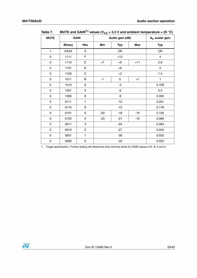
Table 7. MUTE and GAIN(1) values (VCC = 3.3 V and ambient temperature = 25 °C)
1. Target specification. Further testing will determine final min/max limits for GAIN values of E, B, 5 and 4.
MUTE GAIN Audio gain (dB) AV. scalar gain
Binary Hex Min Typ Max Typ
1 XXXX X Off Off
0 1111 F +12 4
0 1110 E +7 +9 +11 2.8
0 1101 D +6 2
0 1100 C +3 1.4
0 1011 B -1 0 +1 1
0 1010 A -3 0.708
0 1001 9 -6 0.5
0 1000 8 -9 0.355
0 0111 7 -12 0.251
0 0110 6 -15 0.178
0 0101 5 -20 -18 -16 0.126
0 0100 4 -23 -21 -19 0.089
0 0011 3 -24 0.063
0 0010 2 -27 0.045
0 0001 1 -30 0.032
0 0000 0 -33 0.022
Audio section operation M41T00AUD
30/42 Doc ID 13480 Rev 5
7.1 GainThe programmable gain stage follows the band pass filter. It provides between –33 and +12 dB of gain, in 3 dB steps (+/-1 dB per step). The gain is selected by the GAIN bits, D3-D0 of register 08h, as listed in Table 4. A MUTE bit, D4 of the same register, allows the audio to be cut off altogether.
At the first power-up, GAIN will be initialized to its lowest value, 0, corresponding to a gain of –33 dB. Furthermore, MUTE will be set thus cutting off all audio.
On subsequent power-ups, GAIN is unaffected, but the MUTE bit is always set to turn off the audio at power-up.
The final section is the output driver. It has a differential output capable of driving 300mW into an 8 Ω load.
The overall gain of the M41T00AUD is defined as the ratio of the AC output voltage, AOUT, and the AC input voltage, SIN, as shown in Figure 16. The 0.1 uF input coupling capacitor blocks any DC in the input signal.
Equation 1 Overall gain = AOUT / SIN
AOUT is measured between the output pins AOUT+ and AOUT–.
AOUT = AOUT+ - AOUT–
Each of the output levels is determined by the ratio of the feedback and input resistors along with the GAIN value.
AOUT+ = SIN x AV x R2/R1
AOUT– = -SIN x AV x R2/R1
where AV is the scalar gain as shown in Table 7. Substituting these into Equation 1 above yields:
AOUT = SIN x AV x R2/R1 - (-SIN x AV x R2/R1) = 2 SIN x AV x R2/R1
With R1 = 2*R2, this reduces to AOUT = SIN x AV. Thus, when R1 = 2*R2, the gain levels in Table 7 reflect overall gain of the circuit (at mid-band frequencies, about 1kHz with the indicated 0.1 uF capacitor). For GAIN set to B (0 dB, AV = 1), the output voltage will be equal to the input (±1 dB).
7.1.1 Gain tolerance
Two tolerance parameters apply to the gain levels. As shown in Table 7, upper and lower limits are listed for four of the GAIN values (4, 5, Bh and Eh). For GAIN=Bh, the tolerance is ±1 dB. This means the end-to-end gain of the part, with R1 = 2*R2, will be 0±1 dB. For GAIN = 4, 5 and Eh, the tolerance is ±2 dB. At each of these three settings, as shown in table 7, the gain will be within 2 dB of the listed typical value. For GAIN =E, the end-to-end gain will be between +7 and +11 dB (9±2 dB).
M41T00AUD Audio section operation
Doc ID 13480 Rev 5 31/42
The other parameter pertains to the gain step size, a relative measurement. It is shown in Table 16 as 3±1 dB. For any gain setting in Table 7, the next higher (or lower) setting is guaranteed to be between 2 and 4 dB higher (or lower). For example, even though no upper and lower limits are shown for GAIN = Ch, it is tested to be at 3±1 dB of the case when GAIN=Bh, one step below. If GAIN=Bh tests to -0.5 dB, then GAIN=Ch is tested to have an end-to-end gain of 2.5±1 dB. If GAIN=Bh tests to +0.5 dB, then GAIN=Ch is tested to be 3.5±1 dB.
This applies to all steps except the lowest one (from GAIN=0 to GAIN=1) which is not tested.
In summary, for GAIN=1 to GAIN=Fh, all steps are tested to have a 1dB step size tolerance of the listed 3 dB step size. The unity gain setting, Bh, will have an end-to-end gain of 0±1dB while the three levels for GAIN=4, 5 and Eh are tested to be within ±2 dB of the typical gain values listed in Table 7.
7.2 Wake-up time: TWU
When the device powers on, the bypass capacitor CBIAS will not be charged immediately. As CBIAS is directly linked to the bias of the amplifier, the amplifier will not work properly until the capacitor is charged. The time to reach this voltage is called the wake-up time or TWU and is specified in the electrical characteristics, Table 16, for CBIAS = 1 µF.
Initial conditions M41T00AUD
32/42 Doc ID 13480 Rev 5
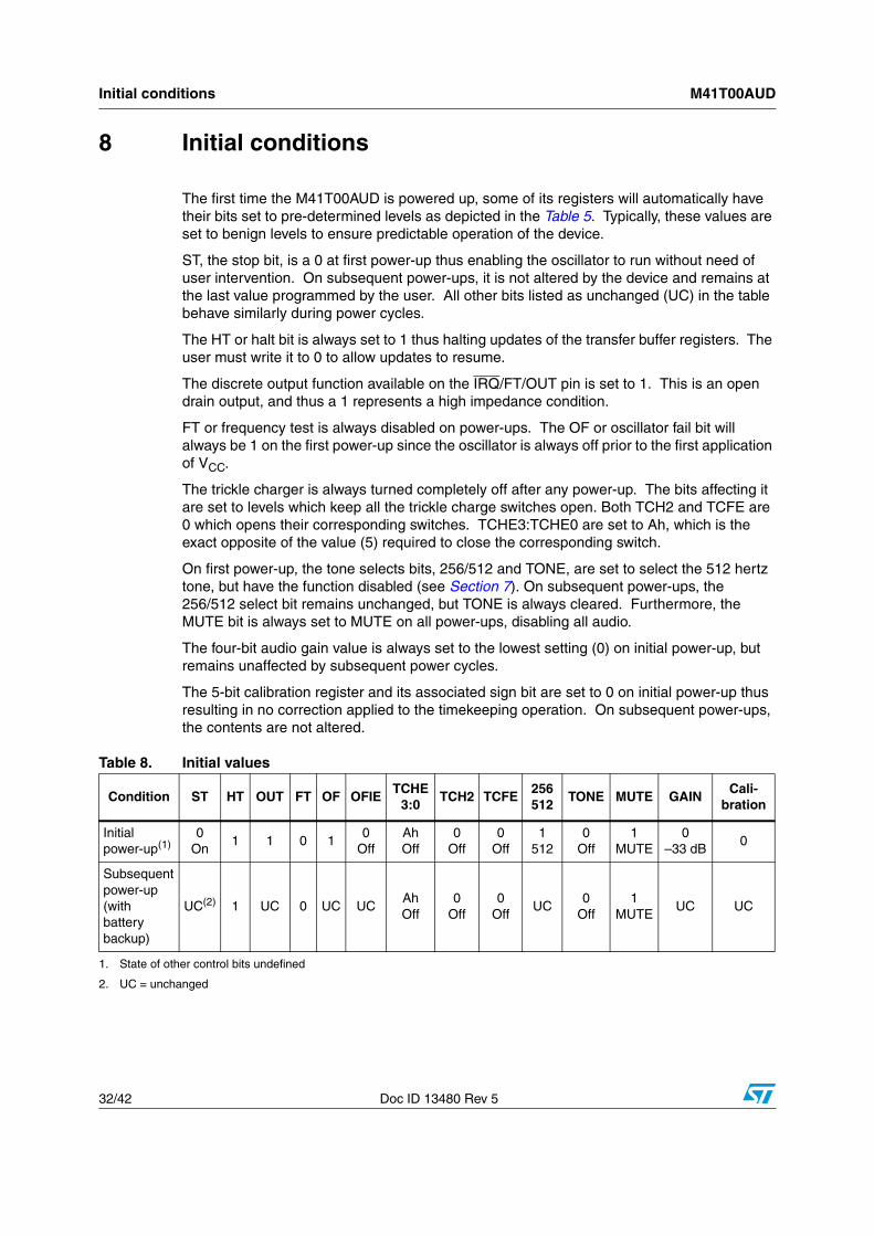
8 Initial conditions
The first time the M41T00AUD is powered up, some of its registers will automatically have their bits set to pre-determined levels as depicted in the Table 5. Typically, these values are set to benign levels to ensure predictable operation of the device.
ST, the stop bit, is a 0 at first power-up thus enabling the oscillator to run without need of user intervention. On subsequent power-ups, it is not altered by the device and remains at the last value programmed by the user. All other bits listed as unchanged (UC) in the table behave similarly during power cycles.
The HT or halt bit is always set to 1 thus halting updates of the transfer buffer registers. The user must write it to 0 to allow updates to resume.
The discrete output function available on the IRQ/FT/OUT pin is set to 1. This is an open drain output, and thus a 1 represents a high impedance condition.
FT or frequency test is always disabled on power-ups. The OF or oscillator fail bit will always be 1 on the first power-up since the oscillator is always off prior to the first application of VCC.
The trickle charger is always turned completely off after any power-up. The bits affecting it are set to levels which keep all the trickle charge switches open. Both TCH2 and TCFE are 0 which opens their corresponding switches. TCHE3:TCHE0 are set to Ah, which is the exact opposite of the value (5) required to close the corresponding switch.
On first power-up, the tone selects bits, 256/512 and TONE, are set to select the 512 hertz tone, but have the function disabled (see Section 7). On subsequent power-ups, the 256/512 select bit remains unchanged, but TONE is always cleared. Furthermore, the MUTE bit is always set to MUTE on all power-ups, disabling all audio.
The four-bit audio gain value is always set to the lowest setting (0) on initial power-up, but remains unaffected by subsequent power cycles.
The 5-bit calibration register and its associated sign bit are set to 0 on initial power-up thus resulting in no correction applied to the timekeeping operation. On subsequent power-ups, the contents are not altered.
Table 8. Initial values
Condition ST HT OUT FT OF OFIETCHE
3:0TCH2 TCFE
256512
TONE MUTE GAINCali-
bration
Initialpower-up(1)
1. State of other control bits undefined
0On
1 1 0 10
OffAhOff
0Off
0Off
1512
0Off
1MUTE
0–33 dB
0
Subsequent power-up (with battery backup)
UC(2)
2. UC = unchanged
1 UC 0 UC UCAhOff
0Off
0Off
UC0
Off1
MUTEUC UC
M41T00AUD Maximum ratings
Doc ID 13480 Rev 5 33/42
9 Maximum ratings
Stressing the device above the rating listed in the absolute maximum ratings table may cause permanent damage to the device. These are stress ratings only and operation of the device at these or any other conditions above those indicated in the operating sections of this specification is not implied.
Exposure to absolute maximum rating conditions for extended periods may affect device reliability. Refer also to the STMicroelectronics SURE Program and other relevant quality documents
Caution: Negative undershoots below –0.3 V are not allowed on any pin while in the backup mode.
Table 9. Absolute maximum ratings
Symbol Parameter Value Unit
TSTG Storage temperature (VCC off, oscillator off) –55 to 150 °C
TJ Maximum junction temperature 150 °C
RTHJA Thermal resistance junction to ambient 200 °C/W
VCC Supply voltage –0.3 to 4.5 V
TSLD(1)
1. Reflow at peak temperature of 260 °C. The time above 255 °C must not exceed 30 seconds.
Lead solder temperature for 10 seconds 260 °C
VIO Input or output voltages –0.3 to Vcc + 0.3 V
IOA Audio output current 300 mA
IOD Digital output current 20 mA
PD Power dissipation Internally limited
DC and AC parameters M41T00AUD
34/42 Doc ID 13480 Rev 5
10 DC and AC parameters
This section summarizes the operating and measurement conditions, as well as the DC and AC characteristics of the device. The parameters in the following DC and AC characteristic tables are derived from tests performed under the measurement conditions listed in the relevant tables. Designers should check that the operating conditions in their projects match the measurement conditions when using the quoted parameters.
Figure 17. AC testing input/output waveform
Table 10. Operating and AC measurement conditions(1)
1. Output Hi-Z is defined as the point where data is no longer driven.
Parameter M41T00AUD
Supply voltage (VCC) 3.0 to 3.6 V
Ambient operating temperature (TA) 0 to 70 °C
Digital load capacitance (CL) 100 pF
Audio load resistance (RL) ≥ 8 Ω
Digital input rise and fall times ≤ 5 ns
Digital input pulse voltages 0.2VCC to 0.8VCC
Digital input and output timing reference voltages 0.3VCC to 0.7VCC
Table 11. Input/output characteristics (25 °C, f = 1 MHz)
Symbol Parameter (1)
1. Effective capacitance measured with power supply at 3.3 V; sampled only, not 100% tested
Min Max Unit
CIND Input capacitance, digital inputs 7 pF
COUTD(2)
2. Outputs deselected
Output capacitance, digital outputs 10 pF
tLP I2C low-pass filter input time constant (SDA and SCL) 50 ns
AI02568
0.8VCC
0.2VCC
0.7VCC
0.3VCC
M41T00AUD DC and AC parameters
Doc ID 13480 Rev 5 35/42
Table 12. DC characteristics
Symbol Parameter Test condition(1) Min Typ Max Unit
ILI Input leakage current 0V ≤ VIN ≤ VCC,
SCL pin±1 µA
ILO Output leakage current0V ≤ VOUT ≤ VCC,OUT and SDA pins
±1 µA
ICC1 Active supply currentNo audio (AIN = VBIAS),
I2C bus active at 400 kHz6.6 14.7 mA
ICC2 Standby supply current
No audio (AIN = VBIAS),
I2C bus not active, SCL = 0 Hz All inputs ≥ VCC – 0.2 V
or ≤ VSS + 0.2 V
6.4 14.3 mA
VIL Input low voltage –0.3 0.3VCC V
VIH Input high voltage 0.7VCC VCC + 0.3 V
VOL
Output low voltage IOL = 3.0 mA 0.4 V
Output low voltage (open
drain)(2) IOL = 3.0 mA 0.4 V
Pull-up supply voltage (open drain)
IRQ/FT/OUT, SDA, SCL Vcc V
VBACK(3) RTC backup supply voltage 1.7 VCC V
IBACK RTC backup supply currentTA = 25 °C, VCC = 0 V
oscillator ON,VBACK = 3 V
0.6 1 µA
1. Valid for ambient operating temperature: TA = 0 to 70 °C; VCC = 3.0 to 3.6 V (except where otherwise noted).
2. For open drain pins IRQ/FT/OUT and SDA
3. STMicroelectronics recommends the RAYOVAC BR1225 or BR1632 (or equivalent) when a battery is used.
Table 13. Crystal electrical characteristics
Symbol Parameter (1)(2) Min Typ Max Units
fO Resonant frequency 32.768 kHz
RS Series resistance 40 KΩ
CL Load capacitance 12.5 pF
1. Externally supplied if using the SO8 package. STMicroelectronics recommends the KDS DT-38: 1TA/1TC252E127, Tuning Fork Type (thru-hole) or the DMX-26S: 1TJS125FH2A212, (SMD) quartz crystal for industrial temperature operations. KDS can be contacted at http://www.kds.info/index_en.htm for further information on this crystal type.
2. Load capacitors are integrated within the M41T00AUD. Circuit board layout considerations for the 32.768 kHz crystal of minimum trace lengths and isolation from RF generating signals should be taken into account.
DC and AC parameters M41T00AUD
36/42 Doc ID 13480 Rev 5
Figure 18. Power down/up mode AC waveforms
Table 14. RTC power down/up AC characteristics
Symbol Parameter(1)(2)
1. Valid for ambient operating temperature: TA = 0 to 70 °C; VCC = 3.0 to 3.6 V (except where otherwise noted).
2. VCC fall time should not exceed 5 mV/µs.
Min Typ Max Unit
tPD SCL and SDA at VIH before power-down 0 ns
trec SCL and SDA at VIH after power-up 10 µs
Table 15. RTC power down/up trip points DC characteristics
Symbol Parameter(1)(2)
1. All voltages referenced to VSS.
2. Valid for ambient operating temperature: TA = 0 to 70 °C; VCC = 3.0 to 3.6 V (except where otherwise noted).
Min Typ Max Unit
VPFD Power-fail deselect 2.60 2.8 2.95 V
Hysteresis 10 mV
VSOBackup switchover voltage(VCC < VBACK; VCC < VPFD)
2.0 < VBACK < VPFD VBACK V
VBACK > VPFD VPFD V
Hysteresis 10 mV
Table 16. Audio section electrical characteristics, valid for VCC = 3.3 V and TAMB = 25 °C (except where otherwise noted)(1)
1. The lowest step, from GAIN = 0 to GAIN = 1, is not tested.
Symbol Parameter Condition Min Typ Max Unit
VOO Output offset voltageNo input signal, RL = 8 Ω
10 100 mV
PO-MAX Maximum output powerTHD = 2% Max, f = 1 kHz,RL = 8 Ω 300 375 mW
PSRRPower supply rejection ratio
RL = 8 Ω, Av = 2,VRIPPLE = 200 mVPP
audio input groundedf = 217 Hz
55 61 dB
Gain step size GAIN steps 1-2 to E-F (1) 2 3 4 dB
TWU Wake-up time after power-up
CBIAS = 1 µF 150 ms
AI00596
VCC
tRECtPD
VSO
SDASCL DON'T CARE
M41T00AUD Package mechanical data
Doc ID 13480 Rev 5 37/42
11 Package mechanical data
In order to meet environmental requirements, ST offers these devices in different grades of ECOPACK® packages, depending on their level of environmental compliance. ECOPACK® specifications, grade definitions and product status are available at: www.st.com. ECOPACK® is an ST trademark.
Package mechanical data M41T00AUD
38/42 Doc ID 13480 Rev 5
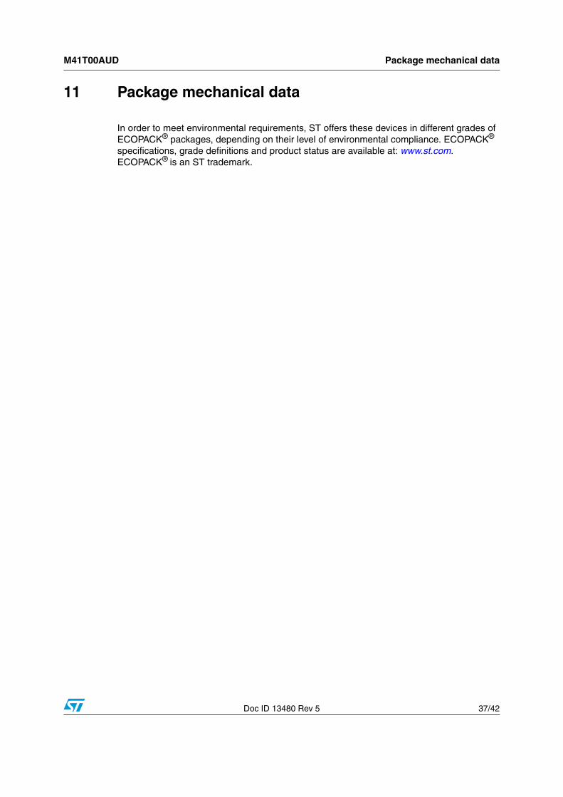
Figure 19. DFN16 (5 mm x 4 mm) package outline
Note: Drawing is not to scale.
INDEX AREA
TOP VIEW
PLANESEATING
BOTTOM VIEW
SIDE VIEW
INDEX AREA
PIN#1 ID
D
E
eb
A1
A
E2
D2
L
k
7964660_C
Table 17. DFN16 (5 mm x 4 mm) package mechanical data
Symmm inches
Min Typ Max Min Typ Max
A 0.80 0.90 1.00 0.032 0.035 0.039
A1 0.00 0.02 0.05 0.0000 0.0008 0.0020
b 0.20 0.25 0.30 0.008 0.010 0.012
D 5.00 0.197
E 4.00 0.158
D2 4.20 4.35 4.45 0.165 0.171 0.175
E2 2.30 2.45 2.55 0.091 0.096 0.100
e 0.50 0.020
k 0.20 0.0078
L 0.30 0.40 0.50 0.012 0.016 0.020
M41T00AUD Package mechanical data
Doc ID 13480 Rev 5 39/42
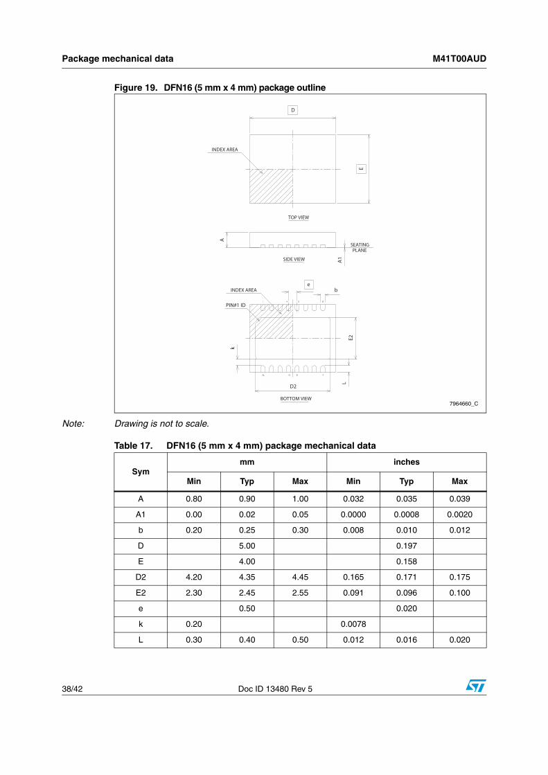
Figure 20. DFN16 (5 mm x 4 mm) footprint
7964660_B
Part numbering M41T00AUD
40/42 Doc ID 13480 Rev 5
12 Part numbering
Table 18. Ordering information scheme
Example: M41T00AUD D 1 F
Device type
M41T00AUD
Package
D = Lead-free 5 mm x 4 mm DFN
Temperature range
1 = 0 °C to 70 °C
Shipping method
E = ECOPACK® lead-free ICs in tube
F = ECOPACK® lead-free ICs in tape & reel
M41T00AUD Revision history
Doc ID 13480 Rev 5 41/42
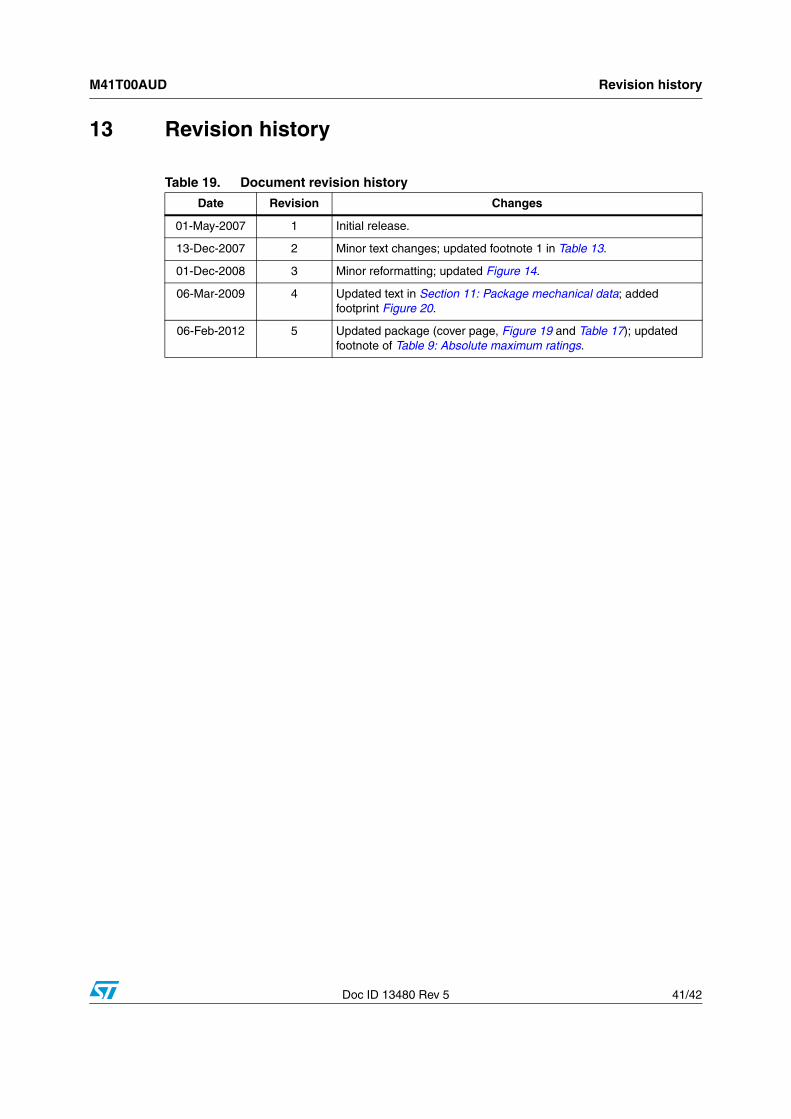
13 Revision history
Table 19. Document revision history
Date Revision Changes
01-May-2007 1 Initial release.
13-Dec-2007 2 Minor text changes; updated footnote 1 in Table 13.
01-Dec-2008 3 Minor reformatting; updated Figure 14.
06-Mar-2009 4 Updated text in Section 11: Package mechanical data; added footprint Figure 20.
06-Feb-2012 5 Updated package (cover page, Figure 19 and Table 17); updated footnote of Table 9: Absolute maximum ratings.
M41T00AUD
42/42 Doc ID 13480 Rev 5
Please Read Carefully:
Information in this document is provided solely in connection with ST products. STMicroelectronics NV and its subsidiaries (“ST”) reserve theright to make changes, corrections, modifications or improvements, to this document, and the products and services described herein at anytime, without notice.
All ST products are sold pursuant to ST’s terms and conditions of sale.
Purchasers are solely responsible for the choice, selection and use of the ST products and services described herein, and ST assumes noliability whatsoever relating to the choice, selection or use of the ST products and services described herein.
No license, express or implied, by estoppel or otherwise, to any intellectual property rights is granted under this document. If any part of thisdocument refers to any third party products or services it shall not be deemed a license grant by ST for the use of such third party productsor services, or any intellectual property contained therein or considered as a warranty covering the use in any manner whatsoever of suchthird party products or services or any intellectual property contained therein.
UNLESS OTHERWISE SET FORTH IN ST’S TERMS AND CONDITIONS OF SALE ST DISCLAIMS ANY EXPRESS OR IMPLIEDWARRANTY WITH RESPECT TO THE USE AND/OR SALE OF ST PRODUCTS INCLUDING WITHOUT LIMITATION IMPLIEDWARRANTIES OF MERCHANTABILITY, FITNESS FOR A PARTICULAR PURPOSE (AND THEIR EQUIVALENTS UNDER THE LAWSOF ANY JURISDICTION), OR INFRINGEMENT OF ANY PATENT, COPYRIGHT OR OTHER INTELLECTUAL PROPERTY RIGHT.
UNLESS EXPRESSLY APPROVED IN WRITING BY TWO AUTHORIZED ST REPRESENTATIVES, ST PRODUCTS ARE NOTRECOMMENDED, AUTHORIZED OR WARRANTED FOR USE IN MILITARY, AIR CRAFT, SPACE, LIFE SAVING, OR LIFE SUSTAININGAPPLICATIONS, NOR IN PRODUCTS OR SYSTEMS WHERE FAILURE OR MALFUNCTION MAY RESULT IN PERSONAL INJURY,DEATH, OR SEVERE PROPERTY OR ENVIRONMENTAL DAMAGE. ST PRODUCTS WHICH ARE NOT SPECIFIED AS "AUTOMOTIVEGRADE" MAY ONLY BE USED IN AUTOMOTIVE APPLICATIONS AT USER’S OWN RISK.
Resale of ST products with provisions different from the statements and/or technical features set forth in this document shall immediately voidany warranty granted by ST for the ST product or service described herein and shall not create or extend in any manner whatsoever, anyliability of ST.
ST and the ST logo are trademarks or registered trademarks of ST in various countries.
Information in this document supersedes and replaces all information previously supplied.
The ST logo is a registered trademark of STMicroelectronics. All other names are the property of their respective owners.
© 2012 STMicroelectronics - All rights reserved
STMicroelectronics group of companies
Australia - Belgium - Brazil - Canada - China - Czech Republic - Finland - France - Germany - Hong Kong - India - Israel - Italy - Japan - Malaysia - Malta - Morocco - Philippines - Singapore - Spain - Sweden - Switzerland - United Kingdom - United States of America
www.st.com