sensorless position control of brushed dc motor using ripple...
TRANSCRIPT
AN3049 Sensorless Position Control of Brushed DC Motor Using
Ripple Counting Technique
Introduction
Author Aldrin Abacan Maria Loida Canada Mike Gomez Microchip Technology Inc
Cost reduction has always been a factor considered when designing a control system especially formotor control applications In DC motor control sensors such as optical encoders Hall effect sensors andcurrent sense transformers are used to identify speed and position which increases the total number ofcomponents thus the overall system cost To eliminate the use of such sensors a drive technique suchas sensorless motor control that uses motor output voltage and current feedback is commonly used inmotor control drive
Aside from the economic factor the advantages of sensorless techniques include decreasedmaintenance a smaller number of fragile connections and easier miniaturization of the system Howeverone of the challenges with the implementation of sensorless techniques is software complexity which canbe lessened by the MCU peripherals by handling other system processes
This project aims to provide an alternative solution to the traditional and expensive methods of usingsensors to obtain and identify the motor position in precision control applications Examples of suchapplications can be found in car seat adjustments mirror control power windows and car flaps UsingPICreg MCUs and Core Independent Peripherals (CIPs) the ripple counting technique based on thecurrent drawn by the motor can be used These CIPs are utilized to drive the motor with minimum CPUintervention
This application note describes three different Brushed DC (BDC) motor ripple counting solutions Eachsolution has utilized a particular PIC MCU device family The first solution is a low-complexity positioncontrol for a single BDC motor using a low-cost PIC18FXXQ10 device family and external current filteringand conditioning components The second solution is a low-cost single-chip capable of controlling twomotors nonsynchronously using the PIC16F177X device family The third solution is a dual-simultaneousBDC motor control using the PIC16F188XX device family The BDC motor used in testing these solutionsis NIDEC COPAL MG16B-240-AB-00
The three solutions described have the following key features
bull Full-Bridge Motor Controlbull Bidirectional Motor Movementbull 5deg-180deg Configurable Angle Incrementbull Motor Stall Detection and Recoverybull Overcurrent Detection for PIC16F177X
copy 2019 Microchip Technology Inc DS00003049A-page 1
Figure 1 Block Diagram
ADC
CWG
Motor Supply
FIRMWARE(Ripple Counter
Motor Positioning)
EUSART
HLT ShutdownSignal
CWGB
CWGD
PWM1
AnalogInput forDesiredAngle
ForwardButton
Motor ForwardReverse Motion
EEPROM
ReverseButton
CWGA
CWGC
PIC18FXXQ10
TIMER1
CCP
RA2
RB0
RD1
RD2
RD3
RSENSE
FULL-BRIDGEDRIVERCIRCUIT
CurrentMonitorOp Amp
Ref
HomeButton
EndpointButton
RA0
RC6
RB4
RC5
RB1
RB2
C1CLC
BDCMOTOR
Figure 1 shows the block diagram of the ripple counting system based on PIC18FXXQ10 ThePIC18FXXQ10 devices are inexpensive robust and general purpose making them suitable for thisapplication This solution uses CIPs to control the motor
The CIPs used in the design are Complementary Waveform Generator (CWG) Hardware Limit Timer(HLT) and Configurable Logic Cell (CLC) Integrating CIPs with other on-chip peripherals such as Pulse-Width Modulation (PWM) Analog-to-Digital Converter (ADC) Capture Compare and PWM (CCP) andtimers give the system the capacity to be fully functional
AN3049
copy 2019 Microchip Technology Inc DS00003049A-page 2
Table of Contents
Introduction1
1 Sensorless Method of BDC Motor Control 511 Brushed DC Motor Current Ripple 612 PWM Effects on the Ripple 9
2 Ripple to Pulse Conversion 1021 Current Sensing Stage 1122 Signal Conditioning Stage A1223 Signal Conditioning Stage B1324 Comparator Stage16
3 Ripple Counting Solutions 1731 PIC18FXXQ10 Solution1732 PIC16F177X Solution2233 PIC16F188XX Solution 27
4 Motor Safety Features 3141 Motor Stall Detection3142 Overcurrent Detection 32
5 Ripple Counting Performance 33
6 Conclusion36
7 Appendix A Circuit Schematic 37
8 Appendix B MPLABreg Code Configuration (MCC) Peripheral Initialization 4081 PIC18FXXQ10 Solution MCC Initialization4082 PIC16F177X Solution MCC Initialization4283 PIC16F188XX Solution MCC Initialization 44
9 Appendix C Source Code Listing46
The Microchip Web Site 47
Customer Change Notification Service47
Customer Support 47
Microchip Devices Code Protection Feature 47
Legal Notice48
Trademarks 48
Quality Management System Certified by DNV49
AN3049
copy 2019 Microchip Technology Inc DS00003049A-page 3
Worldwide Sales and Service50
AN3049
copy 2019 Microchip Technology Inc DS00003049A-page 4
1 Sensorless Method of BDC Motor ControlThe sensorless motor control is a type of drive technique that does not rely on sensors to determine theactual motor position or speed It determines the position of the motor based on electrical parameterssuch as Back-EMF or motor current feedback which is present during the motor run-time
The current feedback is used for circuit protection motor speed estimation or position control The motorcurrent can be monitored by placing a current sense resistor in a series with the motor Using a currentsense amplifier tapped on the resistor terminals the current detected is converted to a measurablevoltage that acts as a position or speed feedback signal to a closed-loop motor control In this applicationthe periodic variations in current feedback due to BDC motor electro-mechanical construction areobserved
The displacement taken by the motor rotation can be identified by counting the number of those periodicvariations during motor operation The method of using motor current feedback to determine motorposition and speed is referred to as the ripple counting technique and will be discussed and utilized in thisapplication note The periodic variations in a current feedback are shown in Figure 1-1
Figure 1-1 Periodic Variation in a Current Feedback
Variations
Figure 1-2 Current Sense Configuration
VMOTOR
M
VMOTOR
M
(a) HIGH-SIDE CURRENT SENSE
VMOTOR
M
+
-
+
-
VOUT
VOUT
+-
VOUT
(c) BRIDGE-ORIENTEDCURRENT SENSE
(b) LOW-SIDE CURRENT SENSE
AN3049Sensorless Method of BDC Motor Control
copy 2019 Microchip Technology Inc DS00003049A-page 5
The ripple counting technique primarily depends on the motor current feedback to implement asensorless drive Different current sense configurations based on sensing resistor placement can be usedto monitor current feedback and are shown in Figure 1-2
High-side current sensing and bridge-oriented current sensing shown in Figure 1-2 (b) and Figure 1-2 (c)respectively are commonly used for functional safety requirements Though proven effective theseconfigurations require a high-end current sense amplifier with high Common-mode voltage and morecomplex circuitry which is not ideal for this application
The current sensing configuration where the current sense resistor is placed between the motor and theground as shown in Figure 1-2 (a) is referred to as low-side current sensing It has the simplest andmost cost-effective implementation of the sensing configurations based on amplifier selection and circuitcomplexity The average voltage in the sensing resistor is near zero since it is ground referenced It doesnot require high-input Common-mode voltage making it easier to select devices for its design andimplementation It is also immune to voltage spikes or surges which makes it suitable for high-voltagemotor applications
Low-side current sensing has its own limitations The placement of the current sense resistor causes theload not to be ground referenced The resistance introduced by the sensing elevates the low side of theload several millivolts above the ground Without ground reference the short circuit between load andground cannot be detected Despite this disadvantage it is still a good choice for the ripple countingapplication because its simplicity and load are not required to be ground referenced The current sensingmethod will be discussed later in the subsequent sections
11 Brushed DC Motor Current RippleThere are several types of ripple in a spinning motor They can be classified as torque ripple speed rippleand current ripple The torque ripple is characterized by undesirable variation of torque production duringshaft revolution preventing smooth motor rotation and is observable mostly in Low-Frequency mode Thespeed ripples also known as speed fluctuations are induced by parasitic torque pulsations that varyperiodically with rotor position
The current ripple is produced during motor rotation and defined as the low-amplitude current alternationriding on the DC voltage supply This current ripple is a periodic variation in current created by the rotormovement when it connects and disconnects rotor coils to the power supply via the brushes Theproduced current ripple gives an insight about the commutation process happening in a BDC motor Figure 1-3 shows how a three-commutator segment motor rotates and how the rotation produces currentripples or commutator spikes
AN3049Sensorless Method of BDC Motor Control
copy 2019 Microchip Technology Inc DS00003049A-page 6
Figure 1-3 Ripple Production from a Rotating Motor
DC Component
a) b) c)
1 MechanicalRevolution
AC Component
Coil 1
Coil 2
Coil 3
V+
V-
b)
Coil 1
Coil 2
Coil 3 Branch 1
Branch 2
a)
Coil 1
Coil 2Coil 3
V+
V-
CommutatorSegment
Coil 1
Coil 3
Coil 2
Brush 1
Brush 2
Branch 1Branch 2
Coil 1Coil 2
Coil 3
V+
c)
V-
Coil 1
Coil 3
Coil 2
Branch 1Branch 2
i1i2
i1
i1i2
i2
When the BDC motor is turning the brushes short-out adjacent commutator segments that result in acurrent circulating between the segments This causes the Back-EMF of the commutator segments to beshorted out thus producing short duration high-voltage pulses on the motor terminals The high-voltagepulses lower the impedance of the armature thus causing the overall current to rise and generate a
AN3049Sensorless Method of BDC Motor Control
copy 2019 Microchip Technology Inc DS00003049A-page 7
current ripple The periodic shifting of a brush from one coil to another produces a periodic current rippleAlso it can be observed that the ripple waveforms are different from each other
As shown in Figure 1-3 when the signal coming from a rotating motor is displayed on a measuringinstrument the DC component will be immediately observed The AC component or current ripple willonly be seen when this DC component is closely examined The rotating direction of the DC motor in Figure 1-3 is assumed as counterclockwise as indicated by the black arrow inside Figure 1-3 (a) Brush 1is connected to a positive supply and Brush 2 is connected to a negative supply The branch circuit 1which is composed of Coil 1 and Coil 2 has current flow in a clockwise direction from Brush 1 to Brush 2as indicated by the red arrow Meanwhile the branch circuit 2 which is composed of Coil 3 has acounterclockwise current flow from Brush 1 to Brush 2 The flowing current occurred on Branch 1 isdefined as i1 while the flowing current on Branch 2 is defined as i2 The total current of the DC motorfollows the Kirchhoffrsquos current law i=i1 + i2
At the moment when Coil 1 aligns with Brush 1 as shown in Figure 1-3 (b) it will make the voltage acrossBranch 1 decrease because the branch is only composed of Coil 2 Since the supply voltage across thetwo brushes is always kept constant the shorting out of Coil 1 will suddenly increase the current value inBranch 1 while the current in Branch 2 stays the same The effect will be the total current flowing into theDC motor which will rapidly increase
After the sudden shorting out the next event is shown in Figure 1-3-c) Branch 1 will only be composed ofCoil 2 while Branch 2 will be composed of Coil 1 and Coil 3 The current flow direction in Coil 2 stays thesame as well as the voltage across it Meanwhile the current value in Branch 2 abruptly decreases whenthe process of commutation ends In this manner the current ripple is produced as shown in the lower leftcorner of Figure 1-3 with a single ripple waveform subdivided into sections to reflect what is happeningduring the commutation process from Figure 1-3 (a) to (c)
The succeeding ripples are created by the same process of coil and brush contact Note that each coilmust touch the two brushes to complete a rotation Furthermore every coil and brush contact produces adistinct ripple waveform The reason behind this is that coils are constructed differently and the brushesof the motor are also different from each other
The number of brushes and commutator poles are fixed in a specific motor This is why the number ofripples in a complete rotation is constant The ripple repeats in every rotation and the number of ripplesper revolution can be calculated using the equation below
Equation 1-1 Number of Ripples per Revolution = ℎ When dealing with a geared motor the equation above will be multiplied by the gear ratio to get thenumber of ripples per revolution The equation below shows the calculation of ripple in a geared motor
Equation 1-2 Number of Ripples per Revolution Using Geared Motor = ℎ Knowing the number of ripples in a single rotation is important to determine the total number of ripplesneeded to rotate a certain degree of an angle Applying Equation 1-1 in the example in Figure 1-3 can beused to calculate that six ripples are produced in a single revolution of three-commutator poles with twobrushes The current ripples need to be filtered conditioned and converted to logic level series of risingand falling edges in order to be countable by an MCU
AN3049Sensorless Method of BDC Motor Control
copy 2019 Microchip Technology Inc DS00003049A-page 8
12 PWM Effects on the RippleThe simplest way to control the speed of a BDC motor is by controlling its supply voltage The higher thevoltage the higher the resulting speed of the motor The PWM on the low-side MOSFET of the full-bridgedriver is used in many DC motor speed control applications The ratio of lsquoONrsquo and lsquoOFFrsquo time determinesthe motor speed
Since the current ripple is characterized by a low amplitude high-frequency periodic signal anymodulation that periodically changes the driving voltage causes the system not to clearly recognize theripple or lower its signal integrity Figure 1-4 shows the ripple produced by different PWM speedmodulations The PWM speed modulation affects the visibility of the ripple depending on the degree ofmodulation Since this solution focuses on precision control applications the speed modulation is set at100 modulation
Figure 1-4 Ripples Produced at Different PWM Duty Cycles
Ripples produced at 80 PWM
Ripples produced at 90 PWM
Ripples produced at 100 PWM
AN3049Sensorless Method of BDC Motor Control
copy 2019 Microchip Technology Inc DS00003049A-page 9
2 Ripple to Pulse ConversionTo effectively count and convert current ripple into PIC MCU readable pulses the current flowing throughthe BDC motor undergoes various signal conditioning and filtering stages Chronologically the stagesare current sensing stage band-pass filter stage differential amplifier stage and the comparator stage
Figure 2-1 illustrates the output signals of each ripple conversion stage from the raw current signal up tothe digital pulses that will be used as an input to PIC MCUs
Figure 2-1 Ripple Conversion Stages Output Signals
Current Sensing Stage
Signal Conditioning Stage A
Comparator Stage
Signal Conditioning Stage B
To PICMCU
MotorCurrent Signal
reg
Signal amplification is needed in the first three stages since the current signal is too small to be detectedby the comparator Depending on the solution the signal conditioning stages and comparator stage canbe external or internal with respect to the PIC MCU family used
All passive components and amplifiers are powered by a 5V supply For the external-based filteringsolutions (PIC16F188XX and PIC18FXXQ10) MCP6024 a quad in the package operational amplifier (opamp) integrated circuit is used It features a wide bandwidth (10 MHz) and low noise feature that aresuitable for small signal processes For the comparator stage an MCP6541 a push-pull output sub-microamp comparator is used While PIC16F177X promotes a cheap single-chip solution PIC18FXXQ10promotes a simple and flexible solution where the signal conditioning and comparator stage are external
The output of the current sense is fed to the microcontroller for the signal conditioning The internal opamp peripheral has a 2 MHz gain bandwidth product and an open loop voltage gain of 90 db It alsooperates from 0V to VDD which is 5V in this application By utilizing these peripherals the Bill of Materials(BOM) costs for hardware designs size and system noise can be reduced The external current sensingstage was designed using MCP6022 For a more detailed schematic diagram refer to 7 Appendix ACircuit Schematic
AN3049Ripple to Pulse Conversion
copy 2019 Microchip Technology Inc DS00003049A-page 10
21 Current Sensing StageSince the application requires a simple and cost-effective implementation the low-side current senseconfiguration is used in this application The current through the bridge driver is detected by tapping adifferential amplifier across the terminals of the current sense resistor R1 which is placed before theground as shown in Figure 2-2
The current sense resistor at the low-side of the driver allows ripple conversion to operate bidirectionallysince the current flow direction will not change when triggered If the current sense resistor is placedwithin the load terminals of a bridge configuration a more complex and more expensive circuitconfiguration is required
Figure 2-2 Current Sense Amplifier Configuration
+‐
IM
R8 R6
R7
C5
R16
C4
R4
R5
VR
EF
R1 ( R SENSE)
FROM M OSFET BRIDGE
R9+
‐
OUTV
The value of R1 depends on the maximum current that could flow throughout the bridge In this designthe current is not expected to exceed 5A The value of the current sense resistor can be calculated using Equation 2-1 Another consideration when picking the right resistor is its power rating which alsodetermines the package size For this application a 2W resistor with a 2512 package size is chosen
Equation 2-1 Current Sense Resistor Value = minus max
AN3049Ripple to Pulse Conversion
copy 2019 Microchip Technology Inc DS00003049A-page 11
Figure 2-3 Voltage Reference Configuration
+‐
VR
EF
5V
R14
C6 R13
Aside from the current sense amplifier the configuration for the current sense voltage biasing is neededSince all stages use a single supply operational amplifier this is more susceptible to saturation during thenegative signal swing It might cause clipping that will affect the original signal Figure 2-3 shows a stablevoltage bias with VREF established by using a unity gain configuration op amp fed by a voltage divider Toobtain the maximum voltage signal swing allowed before saturation the VREF is centered between thevoltage source and the ground VREF is set at 25V on all succeeding stages
The current that flows through the current sense resistor is so small that it requires high-gainamplification Because of this the gain is set to 110VV The VOUT can be solved using the equationbelow
Equation 2-2 Current Sense Resistor Value = + 22 Signal Conditioning Stage A
After the current sensing stage the signal will undergo in a two-stage signal conditioning The first signalconditioning stage is implemented using an active band-pass filter Figure 2-4 shows the band-pass filterconfiguration used in this application This stage is used to eliminate the DC component of the signal andthe added external noise from the previous stage It is also designed to allow frequency withinapproximately 100 Hz to 1500 Hz which is based on the ripple frequency range The ripple frequencycan be identified by the number of commutator poles gear ratio and the rated speed of the motor asshown in Equation 2-3 Different rated speeds of different motors affect the frequency range to be set
Equation 2-4 shows the gain and cut-off frequencies calculation of the band-pass filter The desired gainis calculated by R2 and R3 depending on the maximum voltage swing before the op amp saturation C2and C3 capacitors can be calculated using the resistor values selected and frequency range An invertingamplifier topology is used to retain the biasing from the previous stage to the next stage of rippleconversion
AN3049Ripple to Pulse Conversion
copy 2019 Microchip Technology Inc DS00003049A-page 12
Figure 2-4 Band-Pass Filter Configuration
+‐
VREF
To Signal Conditioning B
C2
C3
R2
R3
IM
Equation 2-3 Ripple Frequency = 30Ex 960 Hz = 40 240 330Equation 2-4 Band-Pass High and Low Cut-Off Frequency and Gain1 = 1222 2 = 1233 1 = 32Ex 10639 Hz = 12 220Ω 68 156034 Hz = 12 15Ω 68 68 = 15Ω220Ω
23 Signal Conditioning Stage BThe output of the active band-pass filter provides a clean amplified AC signal that is biased along thereference voltage This allows the comparator to detect ripples and convert it to pulse with a frequencyequal to the current ripple frequency Although the output is a clean amplified AC signal an initial currentspike that is further discussed in this section has not been filtered out during this process This conditionleads to the addition of another signal conditioning stage while maintaining the proper biasing for thecomparator
AN3049Ripple to Pulse Conversion
copy 2019 Microchip Technology Inc DS00003049A-page 13
Figure 2-5 Inrush Current on Previous Stages
Inrush Current
During motor start-up motor windings behave as a low-resistance closed circuit causing the system todraw a large amount of current This large amount of current during motor start-up is referred as theinrush current It refers to the electrical current usually flowing through the motor in fractions of a secondafter the motorrsquos power is turned on In this brief time interval the current rapidly increases anddecreases to its steady state as the motor begins to rotate
Figure 2-5 illustrates the current produced during motor start-up This current spike is too large and tooslow not to be filtered out by the previous stage In addition the high pass part of the band-pass filter hasbeen set to 100 Hz at the previous stage This configuration produces a fairly large time constant thatprohibits the DC signal components to stabilize quickly
Since the motor is already running and generating ripple at this point this causes the comparator to missthose start-up ripples The blue and green signals in Figure 2-5 represent the current sense stage andband-pass filter stage respectively Failure to detect and convert the start-up ripple current intocomparator pulses will result in a missed pulse and inaccuracy on the ripple count The problem aboutthe start-up current ripple is addressed by using a differential amplifier stage for the second signalconditioning stage
AN3049Ripple to Pulse Conversion
copy 2019 Microchip Technology Inc DS00003049A-page 14
Figure 2-6 Differential Amplifier Configuration
+
‐R11
R17
R4
RIP
PLE
C9
VREF
R15
Filter
Output
Band-pass
At this stage the output of the band-pass filter is fed to both the positive and negative inputs of adifferential amplifier with a capacitor (C9) and tapped in the positive input as shown in Figure 2-6 Thiscapacitor acts as a low-pass filter that introduces a small amount of delay with respect to the originalsignal This delay highly affects the output of the differential amplifier since the common voltage betweeninputs are being negated The effect of the high-current spike is eliminated while retaining the ripplefrequency component The signal is amplified with a differential gain of approximately 68VV for widesignal swing and rebiased at 25V for the comparator stage
Figure 2-7 Digital Pulse Conversion withwithout Differential Amplifier as Input
Figure 2-7 illustrates the difference between the comparator outputs when the differential amplifier outputis used or not If the band-pass filter is used as input for the comparator the initial ripples might not beconverted to pulses because of the inrush current The greater and faster the change in the amplitudeduring the start-up the greater the possibility of a missed pulse The differential amplifier solves thisissue
AN3049Ripple to Pulse Conversion
copy 2019 Microchip Technology Inc DS00003049A-page 15
24 Comparator StageThis stage follows an inverting hysteresis topology that generates an output of either 0 or 5V signalpulses These output pulses are used as an input to the counting algorithm of the firmware Thecomparator hysteresis function moves the threshold level up or down with respect to the input signal Thisprevents the output pulse from oscillating and avoids switching noise during level transition caused bysmall amounts of parasitic feedback
The reference voltage used on the comparator depends on the behavior of the signal Since differentmotors have different current rating and brush construction the reference voltage signal varies dependingon the motor used Typically the reference is set near the center between the voltage source and theground The voltage reference can be configured using a voltage divider tapped to a feedback resistorThis determines the high and low voltage threshold the comparator will accept Figure 2-8 shows thecomparator circuit with hysteresis using MCP6541 For the PIC16F177X solutions the internalcomparator peripheral is utilized
Figure 2-8 Comparator Stage Schematic
RIPPLE
+
R18
R19PU
LSE
R20
5V
The value of the voltage thresholds depends on the values of the resistor applied For the calculation ofVTL and VTH refer to Equation 2-5 R18 and R19 are set similarly since VTL and VTH are centered at VREFas well
Equation 2-5 Voltage Threshold Range
VTL = R19R20R19 + R20 VCCR19R20R19 + R20 + R18 + R19R18R19 + R18 VOLR19R18R19 + R18 + R20VTH = R19R20R19 + R20 VCCR19R20R19 + R20 + R18 + R19R20R19 + R18 VHLR19R18R19 + R18 + R20
AN3049Ripple to Pulse Conversion
copy 2019 Microchip Technology Inc DS00003049A-page 16
3 Ripple Counting SolutionsThe previous section introduced the method of converting current ripple into readable pulses by either theexternal comparator or the PIC MCUrsquos comparator module The next step is to count these convertedripples and to learn how these ripples are processed using the PIC MCU Three ripple counting solutionsusing PIC MCU families will be discussed thoroughly in this section Each of these solutions offer differentpros and cons the user will decide which solution best fits their design
31 PIC18FXXQ10 SolutionThis solution gives flexibility to the user to choose the desired current filtering and conditioningcomponents The value of the external components can be easily adjusted to suit the motor specificationsfor the accurate conversion of ripples to digital pulses The PIC MCU is used to count the digital pulsesand translate the number of pulses into equivalent motor positions Furthermore the use of a PIC MCU ina solution gives better performance due to added intelligence in the system
311 PIC18FXXQ10 Ripple Counting ImplementationThe counting implementation is achieved through the integration of firmware and peripherals Thefirmware commands to initiate the drive and to start the counting of pulses It also facilitates the recordingand storage of the motorrsquos position in the memory On the other hand the peripherals carry out thecounting of pulses and their comparison to the expected number of ripples that are initialized in thebeginning
Figure 3-1 PIC18FXXQ10 Control Diagram
DesiredAngle
Fault Detection
BDC MOTOR
FULL- BRIDGE DRIVER CIRCUIT
TIMER1 Counting
CWG
PWM
Motor Stall Signal
Full‐BridgeSignal
ActualRippleCount
5‐180 deg
Driver Shutdown
Signal
Analog Input From Potentiometer
EUSART
Firmware Calculation for
Expected Ripple Count and
Direction Control
CCP Peripheral
Expected Ripple Count
Firmware Retrieval of
Actual Ripple Count Verified
Ripple Count
Four Input Buttons4
Ripple Counting
Motor Drive Input References
312 Input ReferencesFigure 3-1 shows the complete signal flow in the system The solution is designed with an analogpotentiometer for selecting the desired angle and four buttons for the motor direction control as an inputto the system Two buttons were assigned per direction In the forward direction one button is for anormal incremental movement and another button is for moving to the endpoint while in the reversedirection there is a button for normal movement and another one for going back to home position The
AN3049Ripple Counting Solutions
copy 2019 Microchip Technology Inc DS00003049A-page 17
range of the incremental angle that the system can handle effectively is from 5deg to 180deg with 5deg incrementper potentiometer adjustment The input angle is processed by the firmware and undergoes a series ofcalculations using equations
Equations were developed for calculating the needed parameters in the firmware depending on the givenmotor specification Motors may differ in the number of commutator poles and gear ratio Equation 3-1 isdeveloped to determine the number of ripples per degree in the movement of a geared motor Meanwhile Equation 3-2 is used to calculate the expected number of ripples to rotate a certain degree of an angleLastly the compare load value in Equation 3-3 computes the value to be loaded into the CCP peripheralwhere the TIMER1 register data will be continuously compared to determine if the target position hasbeen reached
Equation 3-1 Ripple Count per Angle = _ _180degEquation 3-2 Expected Ripple Count = Equation 3-3 Compare Load Value = minus _ gt gt 1+ __
313 Motor Drive SignalThe PWM generates a full-bridge signal with 100 duty cycle to supply the CWG The PWM is set to100 duty cycle since this application does not require the modulation of the motor speed The PWMsignal is directed by the CWG peripheral to its specific channels depending on the chosen CWG modeThe CWG has the capacity to drive the motor in forward and reverse directions which enables the motorto be driven bidirectionally The signal coming from the CWG controls the full-bridge driver circuit whichaccomplishes the actual driving of the motor For the complete discussion of this peripheral operationrefer to TB3118 Complementary Waveform Generator Aside from driving using CWG if the device hasno CWG the user can also use the CLC peripheral for creating a combination of signals from the PWMoutput to drive the motor bidirectionally When the motor is already spinning it is the right time to controlits position and dictate when to stop it This will be discussed further in the next section
314 Counting the Current RippleThe counting implementation is achieved through the integration of firmware and peripherals Thefirmware commands to initiate the drive and to start the counting of pulses The conditioned ripple entersthe PIC MCU and is fed to the TIMER1 peripheral
315 Timer1 ConfigurationThe TIMER1 peripheral is a 16-bit timercounter that can be configured in different modes To learn moreabout the function of the TIMER1 peripheral refer to the discussion of TIMER1 in the device data sheetThis application used the TIMER1 module in Gate Toggle mode The TIMER1 module is set to capturedata every high pulse of the signal The diagram in Figure 3-2 illustrates the operation of TIMER1 in thisapplication
AN3049Ripple Counting Solutions
copy 2019 Microchip Technology Inc DS00003049A-page 18
Figure 3-2 Timer1 Diagram
TMR1GE
T1GTM
TMR1 Gate InputRipple Pulse
T1CKIRipple Pulse
T1GVAL
TMR1 Register Value
T1GPOL
N N + 1 N + 2 N + 3
The input to the TMR1 gate and to the TIMER1 clock source is the same because the pulses counted willcome from the clock source and the indicator that needs to be captured is rendered by the pulses comingfrom the gate In the first full-cycle of gate signal the TxGVAL value goes high and low to the succeedingfull-cycle of the ripple signal If this happens alternately the two ripples of the original signal will beequivalent only to a full cycle of TxGVAL
Only when TxGVAL is high the TIMER1 increments its register value and whenever TxGVAL is low theTIMER1 register holds the value accumulated previously In this way two ripples are reduced into a singlepulse in which the TIMER1 register value counts That is the reason why during the setting ofcompareLoadValue in Equation 3-3 it is shifted once to the right to resemble that the expected number ofripples is divided into half The initial value loaded to the TMR1 register is equivalent to half of itsmaximum for a wider range of the desired angle that the TIMER1 can accommodate The TIMER1 countsthe number of ripples but without any position indicator it will not be known if the desired position hasbeen reached The CCP peripheral serves as an indicator when the position is reached
316 CCP OperationThe CaptureComparePWM module is a peripheral that allows the user to time and control differentevents and to generate PWM signals This application uses this peripheral in Compare mode whichallows the user to trigger an event after a predetermined amount of time has expired TIMER1 is thechosen timer to adjust the Compare trip point This mode has a Compare register where the user can putthe value to which the TIMER1 register data will be compared For the TIMER1 and CCP to functionproperly the TIMER1 register and CCP register must have the same initial value In CCP this initial valuewill be added to the expected ripple count to establish the correct reference count
While retrieving the actual ripple count the period timer value equal to the initial value is added to thecontent of the TIMER1 register to get the actual number of ripples that the motor rotated In Equation 3-3the variable compareLoadValue has an added constant INITIAL_TIMER_VALUE to indicate that theTIMER1 register has an initial value from where it will start counting The CALIBRATION_VALUE is aconstant that is being deducted from the total count of expected ripples to compensate for the excessmovement of the motor due to inertia It is dependent on the type of motor used and is obtained bycounting the excess ripples of the motor running in its rated voltage These excess ripples can no longer
AN3049Ripple Counting Solutions
copy 2019 Microchip Technology Inc DS00003049A-page 19
be converted into digital pulses because of their very small amplitude When the TIMER1 value and CCPvalue became equal the CCP generates an interrupt that triggers the motor to stop and retrieve the ripplecount
317 Getting the Ripple CountThe actual ripple count in Equation 3-4 comes from the TIMER1 register added to the period timer valuesubsequently the combined value is shifted once to the left This equation reverses the previousoperation made in the setting of the expected number of ripples in Equation 3-3 This operation is neededin order to properly count the ripples and compensate for the limitation of the Gate Toggle mode
Equation 3-4 Actual Ripple Count = 1_ + _1_ lt lt 1Equation 3-5 Angle Turned = The actual angle that the motor turned is calculated using Equation 3-5 All computations are performedby the firmware After getting all the values EUSART is used to display the actual number of ripples andactual angle It is important that the position is displayed for the user to know if the desired angle hasbeen rotated
318 Braking MechanismJust as starting the motor is important stopping the motor in this application has been very critical tooThe H-Bridge driver must be considered to avoid current shoot-through which may take place if the twoswitches on the same side turned on simultaneously The braking mechanism of the motor isaccomplished through the firmware The CWG is configured to Steer mode and a specific value is writtento CWG1STR to turn on the full-bridge driver low-side switches
In this manner the motor is shorted to ground by turning off the two high-side switches and turning on thetwo low-side switches When the motor terminals are shorted to ground the BEMF across the motor willcause the current to flow to the lower potential which is the ground that immediately drains the energyacross the motor This braking mechanism is applicable to both forward and reverse motor drive
319 Motor PositioningThere are two functions created for processing the angle one for Forward mode and another for Reversemode of the motor This is necessary for establishing the home and endpoint of the motorrsquos positionFrom home the motor can only move using the Forward mode The motor may turn several times beforereaching the endpoint depending on the incremental angle chosen or the user can press the endpointbutton to immediately reach the endpoint Upon reaching the endpoint an LED will light up to indicatethat the motor has reached the endpoint
If the user insists on pressing the button that causes forward motion the motor will not rotate and will staystill This time the user can use the reverse button to turn backward depending on the desired angle setor home button to go back home Similar with Forward mode upon reaching home an indicator LED willlight up to signify that the home is already reached and the button that triggers reverse movement will bedisabled After every motor movement the position will be recorded and stored in the EEPROM addressThis EEPROM address is read at the beginning of the next motor movement of the motorrsquos position inorder to be kept updated
AN3049Ripple Counting Solutions
copy 2019 Microchip Technology Inc DS00003049A-page 20
Figure 3-3 PIC18FXXQ10 Firmware Execution
Start
ReadMotorPositionFromEEPROM()
ReadInput()
Check Buttons
SYSTEM_Initialize()
Enable Interrupts
getCountDonegetCountDone=0
GetAngleTurned() MotorPosition()
getCountDone
motorStalled
StallDetection_Initialize()
motorStalled=0 GetAngleTurned() MotorPosition() __delay_ms(5000) ResumeMotor()
Compare_Initialize()
Yes
No
Yes
No
Figure 3-3 shows the firmware flowchart of the solution The firmware is developed through the aid of theMPLABreg Code Configurator (MCC) The instructions for setting up the peripheral configurations used inthis application can be found in 8 Appendix B MPLABreg Code Configuration (MCC) PeripheralInitialization
The firmware flow starts with a SYSTEM_Initialize() routine This routine initializes pin configurationoscillator and all the peripherals used in the application After system initialization it is necessary toenable interrupts to address the functions requiring interrupts such as Stall_ISR() andCompare_ISR() Compare_Initialize() routine initializes the Compare_ISR() as the Compareinterrupt handler Compare_ISR() is the function that will be executed whenever compare peripheralgenerates an interrupt StallDetection_Initialize() routine sets up the protection feature of thisapplication
AN3049Ripple Counting Solutions
copy 2019 Microchip Technology Inc DS00003049A-page 21
When all the initialization is done the firmware will be in a continuous loop executing the tasks as followsReadMotorPositionFromEEPROM()routine is responsible for reading the motorrsquos position which isnecessary for the firmware to be kept updated on the motorrsquos current position before another rotationbegins The next routine is ReadInput() which gets the data from the potentiometer to select thedesired angle that the motor will turn and computes the equivalent number of expected ripples for aspecific desired angle Check buttons are composed of four subroutines responsible for monitoring if aparticular button is pressed and it initiates the movement in a specific direction After pressing a buttonthe motor rotation and counting of pulses will start at the same time and continue rotation until a specificrotational position is reached
When the position is reached the getCountDone value will be set to lsquo1rsquo (which will be tested in the mainloop) and if the condition is satisfied the program will proceed to GetAngleTurned() andMotorPosition() The GetAngleTurned() routine obtains the actual ripple count and calculates thecorresponding actual angle turned While MotorPosition() routine adds the angle turned to theprevious position and stores the combined latest and previous position to the EEPROM The conditionwith a motorStalled test variable will only be satisfied if the motor is stalled (see the 41 Motor StallDetection section) The position of the motor will be stored through GetAngleTurned() andMotorPosition() and will proceed to the position recovery through ResumeMotor() after a 5s delayThe ResumeMotor()routine is responsible for the motor to return to its home position The loop will becontinuously running executing the tasks mentioned above Refer to 9 Appendix C Source CodeListing for the complete source code
32 PIC16F177X SolutionThis solution uses the integration of analog and digital peripherals of the PIC16F177X device family tocreate a one-chip solution The PIC16F177X has a higher cost than all the PIC MCUs used in thisapplication but it has built-in analog peripherals capable of internally converting the ripple signal to digitalpulses Due to the elimination of the external op amp and comparators the overall cost of the systemdecreased However by using an internal comparator the capacity to convert ripple signals into digitalpulses is limited by the internal comparator hysteresis Furthermore one constraint of this solution isrepresented by the fixed IO pins of the analog modules which means that rerouting the analog signal toother pins is not possible
AN3049Ripple Counting Solutions
copy 2019 Microchip Technology Inc DS00003049A-page 22
Figure 3-4 PIC16F177X Block Diagram
RSENSE
ADC
CCPCOG1
BDC MOTOR
1
FULL- BRIDGE DRIVER CIRCUIT
Motor Supply
Current Monitor
Op‐Amp (Signal
Conditioning)
FIRMWARE(Ripple Counter
Motor Positioning)
EUSART
HLT
Shutdown Signals
PWM9
Overcurrent Signal
Analog Input for Desired
Angle
M2 Forward Switch
HEF
M2 Reverse SwitchCOG1 S ignal
COG3COG3 Signal
BDC MOTOR
2FULL-
BRIDGE DRIVER CIRCUIT
CMP3
CMP1
Shutdown Signals
PIC16F177X
FVR
PWM3
Motor Supply
TIMER1
M1 Forward Switch
M1 Reverse Switch
VREF
Filtering and
The block diagram of the solution based on PIC16F177X is shown in Figure 3-4 The PIC16F177X devicefamily is created to support highly integrated applications Through the integration of analog and digitalperipherals a single device can drive a single motor at a time Similar to the PIC18FXXQ10 solution italso uses CIPs in the design of the system such as Complementary Output Generator (COG) andHardware Limit Timer (HLT)
In contrast with the previous solution the signal filtering and conditioning is done using on-board op ampand comparator peripherals The use of on-board peripherals decreased the number of externalcomponents hence lowering the cost of the overall system Furthermore the use of a single chip toreliably control the position of two motors reduced the system cost Though this solution can address thecontrol of two motors it is required that those motors must not operate simultaneously
321 Internal Op Amp for Signal Filtering and ConditioningThe PIC16F177X family of devices have built-in op amp peripherals In this application the internal opamp modules are used on an inverting configuration The first internal op amp has the same functionalityas the first external op amp in the PIC18FXXQ10 solution It is used for eliminating the signalrsquos DCcomponent and external noises The second op amp is used in the differential amplifier configuration toensure that the signal will be detected by the comparator to prevent missed pulses during the motor start-up After these two stages the signal is fed to the comparator for digital conversion
AN3049Ripple Counting Solutions
copy 2019 Microchip Technology Inc DS00003049A-page 23
322 PIC16F177X Ripple Counting ImplementationFigure 3-5 Control Diagram
DesiredAngle
Fault Detection
BDC MOTOR2
FULL-BRIDGEDRIVERCIRCUITTIMER1 Counting
COG3
Motor Stall Overcurrent Signal
Actual Ripple Count
5‐180deg
Shutdown Signal
EUSART
Firmware Calculation for Expected Ripple Count and Direction
Control
CCP Peripheral
Expected Ripple Count
Verified Ripple Count
PWM9
Full‐Bridge Signal
COG1
Full‐Br idge Signal
PWM3FULL-
BRIDGEDRIVERCIRCUIT
Fault Detection
BDC MOTOR1
Ripple Pulses from MOTOR 2
Motor Stall Overcurrent Signal
Shutdown Signal
Ripple Pulses from MOTOR 1
Firmware Retrieval of
Actual Ripple Count
A nalog Input From Potentiometer
Four Input Buttons4
Input References
Ripple Counting
Motor 1 Drive
Motor 2 Drive
323 Input ReferencesFigure 3-5 shows the complete signal flow of the solution based on the PIC16F177X devices Themanner of setting the desired angle and calculation of expected ripples are similar to the first solutionThe range of the angle that this system can handle is also from 5-180deg with a 5deg configurable angleincrement For the direction control there are four buttons used as an input to the system (two buttonsper motor for bidirectional control) This solution utilized all the equations used in PIC18FXXQ10 forgetting the ripple count per angle (Equation 3-1) expected ripple count (Equation 3-2) and compare loadvalue (Equation 3-3) that will be loaded into the CCP register After processing all the inputs the motor issetup to be driven
324 Motor Drive SignalThe drive signal of the motor is provided by the COG peripheral COG is built in the functionality of CWGwith improved performance and additional features For more information on the operation of the COGperipheral refer to TB3119 Complementary Output Generator Each motor is driven by a dedicatedCOGx The signal coming from the COGx controls the full-bridge driver circuit which accomplishes theactual driving of the motors After successfully driving the motor the BEMF signal is fed to the series ofinternal operational amplifiers for filtering and conditioning The processed signal is internally connectedto the comparator for ripple conversion
325 Counting the Current RippleWhen the ripples are transformed to rectangular pulses they can already be counted by TIMER1 butthere is no comparator option in the TIMER1 clock input source and TIMER1 gate input The comparatoroutput cannot be connected internally to the TIMER1 input To address this issue the comparator outputis channeled externally and then fed back to the TIMER1 clock input and TIMER1 gate input throughanother input pin The counting of the pulses followed the same principle implemented in the Q10solution The TIMER1 and CCP modules have the same configuration with the first solution
Only a pair of TIMER1 and CCP is used for counting the ripple because the motors will only be drivenone at a time The expected ripple count is initially loaded to CCP then the TIMER1 started its counting at
AN3049Ripple Counting Solutions
copy 2019 Microchip Technology Inc DS00003049A-page 24
the same time as the motor is driven When the TIMER1 register value equates the CCP register valuethe actual ripple count is retrieved in the firmware using Equation 3-4 Afterwards the angle turned iscomputed from the actual ripple count value using Equation 3-5 The values are displayed throughEUSART and managed for the home and endpoint establishment Since motors are treatedindependently they also have separate memory addresses for storing the motorrsquos position After everymeasurement the value is stored in the motor memory address and retrieve at the beginning of everymotor movement The High Endurance Flash (HEF) memory which is available in the PIC16F177Xfamily is used for storing the position data
326 Braking MechanismThe braking mechanism used in this solution is similar to the one in the first solution The COGx isconfigured to Steer mode and a specific value is written to COGxSTR to turn on the full-bridge driver low-side switches In this manner the motor is shorted to ground by turning off the two high-side switches andturning on the two low-side switches When the motor terminals are shorted to ground the BEMF acrossthe motor will cause the current to flow to the lower potential which is the ground that immediately drainsthe energy across the motor This braking mechanism is applicable to both forward and reverse motordrive
AN3049Ripple Counting Solutions
copy 2019 Microchip Technology Inc DS00003049A-page 25
Figure 3-6 PIC16F177X Firmware Execution
Start
ReadMotorPositionFromHEF()
ReadInput()
Check Buttons
SYSTEM_Initialize()
Enable Interrupts
getCountDone
getCountDone =0 actualRippleCount =
GetActualRippleCount()
getCountDone faultDetected
StallDetection_Initialize()
__delay_ms(5000) ResumeMotor()
Compare_Initialize()
OvercurrentDetection_Initialize()
motor01
Motor02Position()
Motor01Position()
faultDetected = 0 actualRippleCount =
GetActualRippleCount()
motor01 Motor01Position()
Motor02Position()
No
Yes
No
Yes
Yes Yes
No No
Figure 3-6 shows the firmware flow of the solution based on the PIC16F177X devices The functionsused are almost similar to the routines used in the PIC18FXXQ10 solution But there are some additionalroutines like OvercurrentDetection_Initialize() which initializes the Overcurrent_ISR asthe comparator interrupt handler and will be triggered if an overcurrent occurred in the system Twoseparate routines were created for motor positioning Motor01Position() and Motor02Position()to handle the position of two motors individually and save them to their specific HEF address The testvariable faultDetected will only be satisfied if stall or overcurrent occurred It has similar functionality
AN3049Ripple Counting Solutions
copy 2019 Microchip Technology Inc DS00003049A-page 26
with the motorStall in the PIC18FXXQ10 solution but it addresses two Faults Similar to the firstsolution after the Fault detection took place the actual ripple count is retrieved throughGetActualRippleCount() stored position depending on what motor rotated throughMotor01Position()or Motor02Position() and returned the motor to home throughResumeMotor()after a 5s recovery period Refer to 9 Appendix C Source Code Listing for thecomplete source code
33 PIC16F188XX SolutionThis solution is created for applications requiring simultaneous motor drives such as car mirrors or mudflaps This solution is also developed to control the position of a single motor or two motors concurrentlyThe highlight of this solution is its capacity to drive two motors and control their positions simultaneously
Figure 3-7 PIC16F188XX Block Diagram
Rsense
ADC
SMT1
CWG1BDC
MOTOR 1
FULL-BRIDGE DRIVER CIRCUIT
Motor Supply
Current Monitor
Op-Amp(Signal
Filtering andConditioning)
FIRMWARE(Ripple Counter
Motor Positioning)
EUSART
HLT
Shutdown Signal
PWM2AnalogInput for Desired
Angle
Forward Switch
EEPROM
Reverse Switch
CWG1 Signal
CWG2CWG2 Signal BDC
MOTOR 2
FULL-BRIDGE DRIVER CIRCUIT
Rsense
HLT
Current Monitor
Shutdown Signal
PIC16F188XX
PWM1
Motor Supply
Motor Selector Switch
SMT2
Op-Amp(Signal
Filtering andConditioning)
Set Angle Button
Ref
C1
Ref
C2
The block diagram of the solution based on PIC16F188XX is illustrated in Figure 3-7 The PIC16F188XXfamily is composed of full-featured devices for general purpose and low-power applications Similar to theprevious solutions the drive is accomplished through CIPndashCWG and the functionality of the wholesolution is achieved through the integration of on-chip peripherals and CIPs The conversion of the ripplesignal to digital pulses is accomplished externally similar to the PIC18FXXQ10 implementation
The pulses from two motors are fed to a dedicated SMTx for counting The Signal Measurement Timer(SMT) peripheral is used for counting the ripple pulses The use of SMT made the simultaneous positioncontrol possible because there will be a dedicated hardware counter for each motor SMT is a 24-bitcountertimer with advanced clock and gating logic Refer to 334 Counting the Current Ripple section tolearn how this peripheral is implemented in this application The succeeding section will discuss thecounting implementation of the solution
AN3049Ripple Counting Solutions
copy 2019 Microchip Technology Inc DS00003049A-page 27
331 PIC16F188XX Ripple Counting ImplementationFigure 3-8 PIC16F188XX Control Diagram
Desired Angle
Fault Detection
BDC MOTOR
2
FULL-BRIDGE DRIVER CIRCUIT
SMT2_GetTimerValue
CWG2
Motor Stall Signal
Actual Ripple Count02
Shutdown Signal
EUSART
Firmware Calculation for Expected Ripple
Count01 and RippleCount02
SMT1_SetPeriod()
Expected Ripple Count
Verified Ripple Count
PWM2
Full‐Bridge Signal
CWG1
Full‐Bridge Signal
PWM1
FULL-BRIDGE DRIVER CIRCUIT
Fault Detection
BDC MOTOR
1
Ripple Pulses from MOTOR 2
Motor Stall Signal
Shutdown Signal
Ripple Pulses from MOTOR 1
SMT1_GetTimerValueActual Ripple Count
SMT2_SetPeriod()
Expected Ripple Count02
Firmware Retrieval of
Actual Ripple Count
5‐180degAnalog Input From
Potentiometer
Four Input Buttons4
Input References
Ripple Counting
Motor 1 Drive
Motor 2 Drive
332 Input ReferencesFigure 3-8 shows the complete signal flow of the solution based on the PIC16F188X devices Themanner of setting the desired angle and calculation of expected ripples are similar to the previoussolutions The range of angle that this system can handle is also from 5-180deg with a 5deg configurable angleincrement There are four buttons used as input to the system two buttons were used for direction control(forward and reverse) one of them is used as a motor selector and the other one is used for setting theangle desired for a specific motor in dual motor drive
This solution used all the equations in PIC18FXXQ10 for getting the ripple count per angle (Equation 3-1)and the expected ripple count (Equation 3-2) The expected ripple count is initially loaded to the SMTxPeriod register in which the SMTx Timer register value will be continually compared The SMT peripheralhas an advantage of performing the counting functionality of both CCP and TIMER It is a coreindependent peripheral that reduces the burden on the main core After completing the parameterinitialization the motor is setup to be driven
333 Motor Drive SignalThis solution is created to drive motors individually or simultaneously The integration of the firmware andhardware made it possible to select a specific motor or motors to rotate Similar to the first solution thePWM generates a full-bridge signal with 100 duty cycle to supply the specific CWG The PWM is set to100 duty cycle since this application does not require the modulation of motor speed The PWM signalis directed by the CWGx peripheral to its specific channels depending on the chosen CWGx mode Eachmotor has an independent CGWx driver that provides full-bridge drive signal to the driver circuit Thesignal coming from the CWGx controls the full-bridge driver circuit which accomplishes the actual drivingof the motor The feedback signal from the motor is processed to obtain a series of digital pulses that aresupplied to the SMTx signal input for counting The next segment will show how the ripple pulses arehandled by SMT peripheral
AN3049Ripple Counting Solutions
copy 2019 Microchip Technology Inc DS00003049A-page 28
334 Counting the Current RippleThe main goal of this counting implementation is to count all the ripples until the number of expectedripples is reached To accomplish this the SMTx is configured to Counter mode because this modeenables the ripple pulses to be continuously counted without requiring a window signal The input polarityof the signal is set to rising edge which means that in every rising edge of the signal the SMTx Timerregister value increases
Figure 3-9 SMTx Counting Diagram
SMTxEN
SMTX SignalRipple Pulse
SMTxTMR
SMTxPR
SMTxGO
0 1 3 3602
360
SMTx Interrupt
SMTxPR and SMTxTMR register value matched at this point
4 5 6 7 8 9
Figure 3-9 shows the diagram that describes how counting is performed by SMT The ripples are fed tothe SMTx signal input The SMTx Timer register value increments with every rising edge of the signalWhen the SMTx period equates the value of the SMTx timer an interrupt will occur This match interruptwill trigger the capture of the SMTx timer value that contains the actual ripple count The interrupt will alsotrigger the stopping of the motor which is accomplished using the braking mechanism discussed in thefirst solution The actual ripple count will then be converted to the corresponding angle turned using Equation 3-5
After getting the angle turned the data will be handed to the functions managing the position of themotors The position is stored in the EEPROM after every motor rotation The stored position will beretrieved before another rotation begins for the motorsrsquo position to be kept updated and monitored
AN3049Ripple Counting Solutions
copy 2019 Microchip Technology Inc DS00003049A-page 29
Figure 3-10 PIC16F188XX Firmware Execution
Start
SYSTEM_Initialize()
Enable Interrupts
CheckMotorSelectorButton()
StallDetection_Initialize()
Switch selectMotor
Case 1 MotorDrive01() MotorDrive02()
DualMotorDrive()Case 2
Case 3
switchEvent NextMotor()Yes
No
Figure 3-10 shows the firmware flow of the solution based on the PIC16F188XX devices The process ofinitializing the device through the SYSTEM_Initialize() routine and enabling interrupts is similar tothe PIC18FXXQ10 solution In the continuous loop the CheckMotorSelectorButton()routine is usedto check the button to select the motor that will be driven in the switch-case statements TheMotorDrive01() routine drives motor 1 controls its position and saves it to EEPROM while theMotorDrive02() routine drives motor 2 controls its position and saves it to EEPROM as well TheDualMotorDrive02() routine performs the drive and position control of both motors and stores theposition to the motorsrsquo specific addresses Those are the sequences of the routines that the program hascontinuously executed Refer to 9 Appendix C Source Code Listing for the complete source code
AN3049Ripple Counting Solutions
copy 2019 Microchip Technology Inc DS00003049A-page 30
4 Motor Safety FeaturesIt is of prime importance that the systemrsquos performance will not be adversely affected when it encountersa problem and it must recover after the Fault took place Two safety features used to secure the motor inthe Fault event are discussed below
41 Motor Stall DetectionWhen the motor is spinning freely the ripple pulses are continuously being fed back to the system If themotor halts the trail of digital pulses will also stop The peripheral used for detecting the stall is theHardware Limit Timer (HLT) mode in TIMER246 The primary function of HLT is to monitor any changesin the periodic pulses and its controlled mode is set to roll over pulse
When the signal is absent for resetting the value of HLT it will generate an interrupt which will be used asa trigger to shut down the COGCWG depending on the device family The diagram in Figure 4-1 showsthe HLT implementation in this application
Figure 4-1 HLT Implementation
HLT
COGCWG
FULL -BRIDGE DRIVER CIRCUIT
BDC MOTOR
Comparator
FVR
Conditioned Signal
Shutdown Signal
The comparator output which produces the digital pulses serves as an external reset source to HLT Thedesired period of HLT is set depending on the rated speed of the motor In this application the motorused has a rated speed of 40 RPM This speed expressed in RPM must be converted to a value that willbe loaded to HLT period register which is done using the equation below
The T4PR value must be larger than the value that will be directly calculated from the given speed In thismanner the pulse will occur first and reset the Timer4 count before period match happens With a rotatingmotor the pulses are continuously resetting the Timer4 count avoiding the occurrence of period match
However when the motor is stalled the pulses will not be present to reset the Timer 4 count thus thetimer continues to increment until the period match occurs Every time the period match occurs aninterrupt event is triggered It can be used to shut down the COGCWG and indicate that the motor is in aStall condition
Equation 4-1 RPM to T4PR ConversionT4PR gt RPM TMR4ClockSource Hz60 PrescalerValue PostscalerValueT4PR gt 40 MFINTOSC60 128 1 gt 40 3125060 128 1 gt 162 or 0xA2Note T4PR register value must be greater than 162 or 0xA2
AN3049Motor Safety Features
copy 2019 Microchip Technology Inc DS00003049A-page 31
42 Overcurrent DetectionOvercurrent is a condition where there is an excessive current flow in the motor windings henceexceeding the rated current in which the motor is designed to carry safely and efficiently It can be causedby excessive torque loading short-circuit conductors or an excessive voltage supply To prevent motordamage there must be a way to detect Fault when overcurrent occurs The implementation of thisprotection feature using PIC16F177X is discussed below
Figure 4-2 PIC16F177X Overcurrent Implementation
COGFULL -BRIDGE
DRIVER CIRCUIT
BDC MOTOR
Comparator
FVR
Conditioned Signal
Shutdown Signal
In Figure 4-2 the input is taken from the conditioned signal after the operational amplifier stages Theconditioned signal is fed to the inverting input of the comparator and compared to a reference voltageThis reference voltage results from the product of the current shunt resistance the maximum allowablemotor stall current and gain of the amplifiers used The reference voltage is provided by the FVR Whenovercurrent occurs the conditioned signal voltage will exceed the reference voltage and the comparatorwill generate a signal to trigger the COG auto-shutdown feature
AN3049Motor Safety Features
copy 2019 Microchip Technology Inc DS00003049A-page 32
5 Ripple Counting PerformanceThe results below show the waveforms desired angle calculated expected ripple count actual ripplecount angle turned and percentage error at different angles tested using NIDEC COPAL MG16B-240-AB-00 with the gear ratio of 256 In the motor data sheet it is indicated that the gear ratio is 240 But theresults were inaccurate using this number so it was carefully inspected and the real gear ratio came outto be 256
Figure 5-1 5deg Angular Movement
AN3049Ripple Counting Performance
copy 2019 Microchip Technology Inc DS00003049A-page 33
Figure 5-2 60deg Angular Movement
Figure 5-3 90deg Angular Movement
AN3049Ripple Counting Performance
copy 2019 Microchip Technology Inc DS00003049A-page 34
The difference between the motor operation with and without load has also been observed Figure 5-4shows the signal difference between those conditions At the same 12V of motor voltage the ripplecurrent is greater when there is a load causing a higher voltage swing as the ripple frequency decreasesThe higher voltage swing makes the comparator easily recognize the highlow voltage transition
Figure 5-4 Ripple Conversion withwithout Loading Condition
AN3049Ripple Counting Performance
copy 2019 Microchip Technology Inc DS00003049A-page 35
6 ConclusionThis application note discusses how the ripples were successfully converted to pulses countable by theMicrochip PIC devices These pulses are counted and processed to estimate the position of the motorThe highly-flexible solution is achieved through the PIC18FXXQ10 family the one chip solution is attainedthrough the PIC16F177X family and the dual motor simultaneous BDC motor control is achieved throughthe PIC16F188XX family The implementation of ripple counting in BDC positioning has considerablylowered the total system cost and the motor is protected by safety features in case of Fault event
AN3049Conclusion
copy 2019 Microchip Technology Inc DS00003049A-page 36
7 Appendix A Circuit SchematicFigure 7-1 PIC18FXXQ10 Schematic Diagram
+
-IMR2
C2
C3
R3
VREF
+
-
MCP6024-C
R11
R17
R12
RIPPLE
C9
VRE
F
R15
+
-
5V
+
-
I1
I2
IM
R8
R9
R6
R7
C5
R16
C4
R4
MCP6024-A
MCP6024-B
R14
R13C6
R5
VRE
F
VRE
F
CWGxA
CWGxB
CWGxD
CWGxC
5V
RIPPLE
+
-
MCP6541
R18
R19
PULSE
R20
5V
MOTOR_PIN_A MOTOR_PIN_B
VMOTOR
VMOTOR
MIC4606
TP2
PIC18FXXQ10
VSS
VDD
RB0
RD1
RD2
RD3
5V
RA2PULSE
POT RA0
FWD
REV
END
HOME
RB4
RC5
RB1
RB2
RA4
RA5
RA6
RA7
RC6
C1C8
R1
D1
C11C12
5V
R10
LED1
C7
C1
5V
TP1
TP2
TP3
END_LED
HOME_
LED
STALL_
LED
RIPPLE_
LED
CWGxA
CWGxB
CWGxC
CWGxD
USA
RT_
TX
END_LED
HOME_LED
STALL_LED
RIPPLE_LED
POT
5V
5V
HOME
5V
END
5V
FWD
5V
REV
1 uF1 uF
22 uF 1 uF
LED2 LED3 LED4 LED5I2
I1
SW1SW2
SW3
SW4
1k
1k
1k
1k
220K
220K
1k56 pF
1 nF
10K
10K1 uF
1k1 uF
68 nF 220K
68 pF
15M
22K
22K
1 nF
15M
15M
1 uF
1k
1k
33K
400m
10K
10K
10K
10K
1k
1k1k
1k
10K
1k
1K 1K 1K 1KR21 R22 R23 R24
R25
R26
R27
R28
R29
R30
R31
R32
AN3049Appendix A Circuit Schematic
copy 2019 Microchip Technology Inc DS00003049A-page 37
Figure 7-2 PIC16F177X Schematic DiagramPIC16F188XX
VSS
VDD
RC7
RD4
RD5
RD6
5V
POT RE0
M1_REV
M2_REV
M2_FWD
M1_FWD
RB0
RB5
RA5
RC2
RB2
RD3
RC6
OVER
CURRE
NT_LED
STALL_
LED
COG1A
COG1B
COG1C
COG1D
USA
RT_
TX
RC0
RE1
RA7
RD7
COG3A
COG3B
COG3C
COG3D
RA1
VREF RA4
RB1
+
-
5V
+
-
I1
I2
IM
R9
R6
R7C5
R16
C4
R4
MCP6022-A
MCP6022-B
R14
R5
VRE
F
VRE
F
IM
RD0
RD1
RD2R11 R15
R17
R12
VREF
RA0
RA3
RA6
RIPPLE
RIPPLE
R18
R19
5V
RB3
RC1
PULSE
RIPPLE
RC3SCK
RC4SDI
RC5 SDO
COG1A
COG1B
COG1D
COG1C
5VMOTOR1_PIN_A MOTOR1_PIN_B
VMOTOR
VMOTOR
MIC4606
C1C8
R1
D1
C11C12
COG2A
COG2B
COG2D
COG2C
5VMOTOR2_PIN_BMOTOR2_PIN_A
VMOTOR
VMOTOR
MIC4606
C13 C14
D2
C11 C12
OVERCURRENT_LED
STALL_LED
POT
5V
5V
M1_F
WD
5V
M2_F
wd
5V
M1_R
EV
5V
M2_R
EV
400m
R8
1k
1k 1k
1k
220K
220K
1k
1 nF
10K
R13C610K1 uF
R2C2
22 nF 100K
C3 R3100 pF 15M
22K
22K
C9 1 nF 15M
15M
R20
1K1K 33K
LED1 LED2
R21
1k 1kR22
1k
1k
1k1k
1k
10K
10K 10K
10K
SW1
SW2
SW3
SW4
10KR23
R24
R25
R26
R27
R28
R29
R30
R31
R32
AN3049Appendix A Circuit Schematic
copy 2019 Microchip Technology Inc DS00003049A-page 38
Figure 7-3 PIC16F188XX Schematic Diagram
PIC16F188XX
VSS
VDD
RB4
RB5
RB6
RB7
5V
RC1PULSE1
POT RA0
FWD
REV
MOTOR_SELECT
SET_ANGLE
RA5
RB0
RA7
RA6
RB2
RB3
RD0
RC6
HOME_
LED
END_LED
STALL_
LED
CWG1A
CWG1B
CWG1C
CWG1D
USA
RT_
TX
RC7
RD2
RD3
RD4
CWG2A
CWG2B
CWG2C
CWG2D
RD6PULSE2
5V
SET_AN
GLE
5V
END
5VMOTO
R_
SELECT
5V
REV
END_LED
HOME_LED
STALL_LED
POT
5V
+
-IM1R2
C2
C3
R3
VREF1
+
-
MCP6024-C
R11
R17
R12
RIPPLE
1
C9
VRE
F1
R15
+
-
5V
+
-
I1
I2
IM1
R8
R9
R6
R7
C5
R16
C4
R4
MCP6024-A
MCP6024-B
R14
R13C6
R5
VRE
F1
VRE
F1
RIPPLE1
+
-
MCP6541
R18
R19
PULSE1
R20
5V
TP2
5V
R10
LED1
C7
C1
5V
TP1
TP3
TP4
1k
1k
1k
1k
220K
220K
1k56 pF
1 nF
10K
10K1 uF
1k1 uF
68 nF 220K
68 pF
15M
22K
22K
1 nF
15M
15M
1 uF
1k
1k
33K
CWG1A
CWG1B
CWG1D
CWG1C
5VMOTOR1_PIN_A MOTOR1_PIN_B
VMOTOR
VMOTOR
MIC4606
C1C8
R1
D1
C11C12
1 uF1 uF
22 uF 1 uF
I2I1
400m
CWG2A
CWG2B
CWG2D
CWG2C
5VMOTOR2_PIN_A MOTOR_2_PIN_B
VMOTOR
VMOTOR
MIC4606
C13C14
R21
D2
C16C15
1 uF1 uF
22 uF 1 uF
I4I3
400m
+
-IM2R32
C21
C22
R33
VREF2
+
-
MCP6024-C
R34
R35
R37
RIPPLE
2
C23
VRE
F2
R36
+
-
5V
+
-
I4
I3
IM2
R22
R23
R24
R25
C17
R28
C18
R27
MCP6024-A
MCP6024-B
R29
R30C19
R26
VRE
F2
VRE
F2
RIPPLE2
+
-
MCP6541
R38
R39
PULSE2
R40
5V
TP6
5V
R31
LED2
C20
C24
5V
TP5
TP7
TP8
1k
1k
1k
1k
220K
220K
1k56 pF
1 nF
10K
10K1 uF
1k1 uF
22 nF 100K
100 pF
15M
22K
22K
1 nF
15M
15M
1 uF
1k
1k
33K
LED3 LED4 LED5
SW1SW2
SW3SW4
10K
10K
10K
10K
1k
1k
1k1k
1k
10K1k 1k 1k
R41
R42
R43
R44
R45
R46
R47
R48
R49 R50 R51
R52
R53
AN3049Appendix A Circuit Schematic
copy 2019 Microchip Technology Inc DS00003049A-page 39
8 Appendix B MPLABreg Code Configuration (MCC) PeripheralInitializationMPLABreg Code Configurator is an easy-to-use plugin tool for MPLABreg X IDE that generates codes forcontrolling the peripherals of Microchip microcontrollers based on the settings made in its Graphical UserInterface (GUI) MPLAB Code Configurator is utilized to easily configure the peripherals used in thismotor control application Refer to the MPLABreg Code Configurator Userrsquos Guide (DS40001725) forfurther information on how to install and set up the MCC in MPLAB X IDE
The step-by-step process of using MCC in each of the three solutions of this motor control positioningapplication is discussed in this section
81 PIC18FXXQ10 Solution MCC Initialization1 In the System Module set the clock to HFINTOSC with 32 MHz frequency2 Set the ADCC module to Basic_mode with FOSCADCLK clock source configured to FOSC323 For providing drive signal to the motor three peripherals are needed to be configured CCP2
TIMER2 and CWG Prior to setting the CCP2 in PWM mode the Timer 2 must be enabled withFOSC4 clock source In the CCP2 module choose the PWM mode and select TIMER 2 as theassigned timer and also set the duty cycle to 100 Enable the CCP2 The CWG must beconfigured with CCP2_OUT as an input source with Output mode in Forward Full-Bridge mode andHFINTOSC as the selected clock source Enable the CWG
4 In counting the digital pulses three peripherals are utilized CLC1 CCP1 and TIMER1 The CLC1is used for rerouting the input to TMR1 clock source and gate signal source Configure CLC1 in 4-input AND mode with one gate having the input pulses and the rest of the three AND gatesinverted to produce an output 1 so that CLC1 acts as a buffer Enable the CLC1 The CCP1 mustbe set to Compare mode with TIMER1 as the assigned timer for adjusting its trip point SetCOMPARE in Toggle mode Enable the CCP interrupt and the CCP module Choose the CLC1OUTas a TIMER1 clock source enable the gate and enable Gate Toggle mode with CLC1OUT as thegate signal source and gate polarity as HIGH Put an initial period count of 0x7FFF being half of themaximum count Enable the Timer Gate interrupt but do not enable the TIMER1 yet The TIMER1will be enabled in the program
5 For displaying the data EUSART1 is configured in Asynchronous mode with Transmit enabled anda baud rate of 9600 Under its software settings tick the box next to Redirect STDIO to USART
6 The MEMORY is added to store the data From the Device Resources find the MEMORY anddouble click so that it will be added to the application
7 TIMER4 is configured to its Hardware Limit Timer mode to be used for stall detection The clocksource used is MFINTOSC_3125 kHz with a Prescaler value of 1128 to extend the period rangeand Timer Period set to 100 ms CLC1_OUT is used as an input to the external reset source withRoll Over Pulse Control mode and TIMER4 resets its count every rising of signal on its resetsource Enable the Timer interrupt but do not enable the TIMER4 yet it will be enabled in theprogram
8 In the PIN MANAGER configuration set up the inputoutput pins of all the peripherals as shown in Figure 8-1
9 After configuring all the peripherals click the lsquoGenerate Codersquo button next to the Project Resourcestab name in the top left corner This will generate a mainc file to the project automatically It willalso initialize the module and leave an empty while(1) loop for custom code entry
AN3049Appendix B MPLABreg Code Configuration (MCC) Periph
copy 2019 Microchip Technology Inc DS00003049A-page 40
Figure 8-1 PIC18FXXQ10 Pin Manager Configuration
AN3049Appendix B MPLABreg Code Configuration (MCC) Periph
copy 2019 Microchip Technology Inc DS00003049A-page 41
82 PIC16F177X Solution MCC Initialization1 In the System Module set the clock to INTOSC with 16 MHz frequency2 Set the ADC Clock to FOSC16 clock source3 Three peripherals are needed to be configured for each motor drive TIMER2 is common to both
driving motors since it is used for adjusting the frequency of the PWMx The TIMER2 clock sourceis set to FOSC4 before it is enabled For driving motor 1 PWM3 TIMER2 and COG1 are used Inthe PWM3 module select the TIMER2 as the assigned timer and set the duty cycle to 100Enable the PWM The COG1 must be configured with PWM3 output as an input source to risingand falling event with Output mode in Forward Full-Bridge mode and HFINTOSC is selected as theclock source Enable the COG1 For driving motor 2 PWM9 TIMER2 and COG3 are used In thePWM9 module select the TIMER2 as the assigned timer and set the duty cycle to 100 Enablethe PWM The COG3 must be configured with PWM9 output as an input source to the rising andfalling event with Output mode in Forward Full-Bridge mode and HFINTOSC is chosen as the clocksource Enable the COG3
4 In converting ripples to digital pulses analog peripherals are used OPA1 is used for signal filteringthe positive channel is taken from OPA1IN0+ and the negative channel is supplied from OPA1IN1-OPA4 is used for signal conditioning the positive channel is taken from OPA4IN0+ and thenegative channel is supplied from OPA4IN1- Enable each op amp after setting up the moduleCMP1 is used for converting the conditioned signal to digital pulses with inverted output polarityThe chosen channel for positive input is CIN1+ and for the negative input is CIN0- Enable themodule after choosing the desired configuration
5 In counting the digital pulses two peripherals are utilized CCP1 and TIMER1 The CCP1 must beconfigured to Compare mode with TIMER1 as the assigned timer for adjusting its trip point SelectToggle mode Enable the CCP interrupt and enable the CCP module Choose External as theTIMER1 clock source enable the gate and enable Gate Toggle mode with T1G_pin as the gatesignal source and gate polarity as HIGHS Put an initial period count of 0x7FFF being half of themaximum count Enable the Timer Gate interrupt but do not enable the TIMER1 yet The TIMER1will be enabled in the program
6 For displaying the data EUSART1 is configured in Asynchronous mode with Transmit enabled andbaud rate of 9600 Under its software settings tick the box next to Redirect STDIO to USARTAnother peripheral used for display is MSSP this peripheral is used to communicate with an LCDChoose the SPI Master mode with Clock Polarity (IdleLow ActiveHigh) and Clock Edge set toActive to Idle The SPI clock source is FOSC64
7 The MEMORY is added to store the data From the Device Resources look for the MEMORYmodule and double click it so that it will be added to the application
8 This application is equipped with safety features Stall Detection and Overcurrent Detection ForStall Detection TIMER4 is configured to its Hardware Limit Timer mode The clock source used isMFINTOSC_3125 kHz with a Prescaler value of 1128 to extend the period range and TimerPeriod set to 100 ms C1OUT is used as an input to the external reset source with Roll Over PulseControl mode and TIMER4 resets its count every rising of signal on its reset source
9 In the PIN MANAGER configuration set up the inputoutput pins of all the peripherals as shown in Figure 8-2
10 After configuring all the peripherals click the lsquoGenerate Codersquo button next to the Project Resourcestab name in the top left corner This will generate a mainc file to the project automatically It willalso initialize the module and leave an empty while(1) loop for custom code entry
AN3049Appendix B MPLABreg Code Configuration (MCC) Periph
copy 2019 Microchip Technology Inc DS00003049A-page 42
Figure 8-2 PIC16F177X Pin Manager Configuration
AN3049Appendix B MPLABreg Code Configuration (MCC) Periph
copy 2019 Microchip Technology Inc DS00003049A-page 43
83 PIC16F188XX Solution MCC Initialization1 In the System Module set the clock to HFINTOSC with 32 MHz frequency2 Set the ADCC module to Basic_mode with FOSCADCLK clock source configured to FOSC323 Three peripherals are needed to be configured for each motor drive TIMER2 is common to both
motor drives since it is used for adjusting the frequency of the PWMx The clock source is set toFOSC4 afterwards TIMER2 is enabled For driving motor 1 CCP1 TIMER2 and CWG1 are usedIn the CCP1 module choose the PWM mode and select TIMER 2 as the assigned timer and alsoset the duty cycle to 100 Enable the CCP1 The CWG1 must be configured with CCP1_OUT asan input source with Output mode in Forward Full-Bridge mode and HFINTOSC as the selectedclock source Enable the CWG1 For driving motor 2 CCP2 TIMER2 and CWG2 are used InCCP2 module choose the PWM mode and select TIMER 2 as the assigned timer and also set theduty cycle to 100 Enable the CCP2 The CWG2 must be configured with CCP2_OUT as an inputsource with Output mode in Forward Full-Bridge mode and HFINTOSC as the selected clocksource Enable the CWG2
4 In counting the digital pulses the signal measurement timer is used Since this solution is createdto drive two motors simultaneously each motor has a dedicated SMT counter SMT1 is used forcounting the pulses from Motor 1 It is configured to Counter mode with Repeated Data AcquisitionThe signal input is taken from SMT1SIGPPS with highrising edge input polarity and the periodcount is initialized with the value of 0x7FFFFF Tick the box next to Enable the Match Interrupt andEnable SMT but do not tick the box next to Data Acquisition After Init The Data Acquisition will beenabled in the program While SMT2 is used for counting the pulses from Motor 2 It is configuredto Counter mode with Repeated Data Acquisition The Signal input is taken from SMT2SIGPPSwith highrising edge input polarity and the period count is initialized with the value of 0x7FFFFFTick the box next to Enable the Match Interrupt and Enable SMT but do not tick the box next toData Acquisition After Init The Data Acquisition will be enabled in the program as well
5 For displaying the data EUSART1 is configured in Asynchronous mode with Transmit enabled andbaud rate of 9600 Under its software settings tick the box next to Redirect STDIO to USARTAnother peripheral used for display is MSSP this peripheral is used to communicate with an LCDChoose the SPI Master mode with Clock Polarity(IdleLow ActiveHigh) and Clock Edge set toActive to Idle The SPI clock source is FOSC64
6 The MEMORY is added to store the data From the Device Resources find the MEMORY moduleand double click it so that it will be added to the application
7 For safety features each motor has a dedicated timer for stall detection TIMER4 is configured toits Hardware Limit Timer mode and used for detecting stall in motor 1 The clock source used isMFINTOSC_3125 kHz with a Prescaler value of 1128 to extend the period range and TimerPeriod set to 100 ms The T4CKIPPS pin is used as an input to the external reset source with RollOver Pulse Control mode and TIMER4 resets its count every rising of signal on its reset sourceEnable the Timer interrupt but do not enable the TIMER4 yet it will be enabled in the programWhile TIMER6 is configured to its Hardware Limit Timer mode and used for detecting stall in motor2 The clock source used is the same with TIMER4 The T6CKIPPS pin is used as an input to theexternal reset source with Roll Over Pulse Control mode and TIMER6 resets its count every risingof signal on its reset source Enable the Timer interrupt but do not enable the TIMER6 yet it will beenabled in the program
8 In the PIN MANAGER configuration set up the inputoutput pins of all the peripherals as shown in Figure 8-3
AN3049Appendix B MPLABreg Code Configuration (MCC) Periph
copy 2019 Microchip Technology Inc DS00003049A-page 44
9 After configuring all the peripherals click the lsquoGenerate Codersquo button next to the Project Resourcestab name in the top left corner This will generate a mainc file to the project automatically It willalso initialize the module and leave an empty while(1) loop for custom code entry
Figure 8-3 PIC16F188XX Pin Manager Configuration
AN3049Appendix B MPLABreg Code Configuration (MCC) Periph
copy 2019 Microchip Technology Inc DS00003049A-page 45
9 Appendix C Source Code ListingThe latest software version can be downloaded from the Microchip website (wwwmicrochipcom) Theuser will find the source code appended to the electronic version of this application note The latestversion is v10
AN3049Appendix C Source Code Listing
copy 2019 Microchip Technology Inc DS00003049A-page 46
The Microchip Web Site
Microchip provides online support via our web site at httpwwwmicrochipcom This web site is used asa means to make files and information easily available to customers Accessible by using your favoriteInternet browser the web site contains the following information
bull Product Support ndash Data sheets and errata application notes and sample programs designresources userrsquos guides and hardware support documents latest software releases and archivedsoftware
bull General Technical Support ndash Frequently Asked Questions (FAQ) technical support requests onlinediscussion groups Microchip consultant program member listing
bull Business of Microchip ndash Product selector and ordering guides latest Microchip press releaseslisting of seminars and events listings of Microchip sales offices distributors and factoryrepresentatives
Customer Change Notification Service
Microchiprsquos customer notification service helps keep customers current on Microchip productsSubscribers will receive e-mail notification whenever there are changes updates revisions or erratarelated to a specified product family or development tool of interest
To register access the Microchip web site at httpwwwmicrochipcom Under ldquoSupportrdquo click onldquoCustomer Change Notificationrdquo and follow the registration instructions
Customer Support
Users of Microchip products can receive assistance through several channels
bull Distributor or Representativebull Local Sales Officebull Field Application Engineer (FAE)bull Technical Support
Customers should contact their distributor representative or Field Application Engineer (FAE) for supportLocal sales offices are also available to help customers A listing of sales offices and locations is includedin the back of this document
Technical support is available through the web site at httpwwwmicrochipcomsupport
Microchip Devices Code Protection Feature
Note the following details of the code protection feature on Microchip devices
bull Microchip products meet the specification contained in their particular Microchip Data Sheetbull Microchip believes that its family of products is one of the most secure families of its kind on the
market today when used in the intended manner and under normal conditionsbull There are dishonest and possibly illegal methods used to breach the code protection feature All of
these methods to our knowledge require using the Microchip products in a manner outside theoperating specifications contained in Microchiprsquos Data Sheets Most likely the person doing so isengaged in theft of intellectual property
bull Microchip is willing to work with the customer who is concerned about the integrity of their code
AN3049
copy 2019 Microchip Technology Inc DS00003049A-page 47
bull Neither Microchip nor any other semiconductor manufacturer can guarantee the security of theircode Code protection does not mean that we are guaranteeing the product as ldquounbreakablerdquo
Code protection is constantly evolving We at Microchip are committed to continuously improving thecode protection features of our products Attempts to break Microchiprsquos code protection feature may be aviolation of the Digital Millennium Copyright Act If such acts allow unauthorized access to your softwareor other copyrighted work you may have a right to sue for relief under that Act
Legal Notice
Information contained in this publication regarding device applications and the like is provided only foryour convenience and may be superseded by updates It is your responsibility to ensure that yourapplication meets with your specifications MICROCHIP MAKES NO REPRESENTATIONS ORWARRANTIES OF ANY KIND WHETHER EXPRESS OR IMPLIED WRITTEN OR ORAL STATUTORYOR OTHERWISE RELATED TO THE INFORMATION INCLUDING BUT NOT LIMITED TO ITSCONDITION QUALITY PERFORMANCE MERCHANTABILITY OR FITNESS FOR PURPOSEMicrochip disclaims all liability arising from this information and its use Use of Microchip devices in lifesupport andor safety applications is entirely at the buyerrsquos risk and the buyer agrees to defendindemnify and hold harmless Microchip from any and all damages claims suits or expenses resultingfrom such use No licenses are conveyed implicitly or otherwise under any Microchip intellectualproperty rights unless otherwise stated
Trademarks
The Microchip name and logo the Microchip logo AnyRate AVR AVR logo AVR Freaks BitCloudchipKIT chipKIT logo CryptoMemory CryptoRF dsPIC FlashFlex flexPWR Heldo JukeBlox KeeLoqKleer LANCheck LINK MD maXStylus maXTouch MediaLB megaAVR MOST MOST logo MPLABOptoLyzer PIC picoPower PICSTART PIC32 logo Prochip Designer QTouch SAM-BA SpyNIC SSTSST Logo SuperFlash tinyAVR UNIO and XMEGA are registered trademarks of Microchip TechnologyIncorporated in the USA and other countries
ClockWorks The Embedded Control Solutions Company EtherSynch Hyper Speed Control HyperLightLoad IntelliMOS mTouch Precision Edge and Quiet-Wire are registered trademarks of MicrochipTechnology Incorporated in the USA
Adjacent Key Suppression AKS Analog-for-the-Digital Age Any Capacitor AnyIn AnyOut BodyComCodeGuard CryptoAuthentication CryptoAutomotive CryptoCompanion CryptoController dsPICDEMdsPICDEMnet Dynamic Average Matching DAM ECAN EtherGREEN In-Circuit Serial ProgrammingICSP INICnet Inter-Chip Connectivity JitterBlocker KleerNet KleerNet logo memBrain Mindi MiWimotorBench MPASM MPF MPLAB Certified logo MPLIB MPLINK MultiTRAK NetDetach OmniscientCode Generation PICDEM PICDEMnet PICkit PICtail PowerSmart PureSilicon QMatrix REAL ICERipple Blocker SAM-ICE Serial Quad IO SMART-IS SQI SuperSwitcher SuperSwitcher II TotalEndurance TSHARC USBCheck VariSense ViewSpan WiperLock Wireless DNA and ZENA aretrademarks of Microchip Technology Incorporated in the USA and other countries
SQTP is a service mark of Microchip Technology Incorporated in the USA
Silicon Storage Technology is a registered trademark of Microchip Technology Inc in other countries
GestIC is a registered trademark of Microchip Technology Germany II GmbH amp Co KG a subsidiary ofMicrochip Technology Inc in other countries
All other trademarks mentioned herein are property of their respective companies
AN3049
copy 2019 Microchip Technology Inc DS00003049A-page 48
copy 2019 Microchip Technology Incorporated Printed in the USA All Rights Reserved
ISBN 978-1-5224-4506-7
Quality Management System Certified by DNV
ISOTS 16949Microchip received ISOTS-169492009 certification for its worldwide headquarters design and waferfabrication facilities in Chandler and Tempe Arizona Gresham Oregon and design centers in Californiaand India The Companyrsquos quality system processes and procedures are for its PICreg MCUs and dsPICreg
DSCs KEELOQreg code hopping devices Serial EEPROMs microperipherals nonvolatile memory andanalog products In addition Microchiprsquos quality system for the design and manufacture of developmentsystems is ISO 90012000 certified
AN3049
copy 2019 Microchip Technology Inc DS00003049A-page 49
AMERICAS ASIAPACIFIC ASIAPACIFIC EUROPECorporate Office2355 West Chandler BlvdChandler AZ 85224-6199Tel 480-792-7200Fax 480-792-7277Technical SupporthttpwwwmicrochipcomsupportWeb AddresswwwmicrochipcomAtlantaDuluth GATel 678-957-9614Fax 678-957-1455Austin TXTel 512-257-3370BostonWestborough MATel 774-760-0087Fax 774-760-0088ChicagoItasca ILTel 630-285-0071Fax 630-285-0075DallasAddison TXTel 972-818-7423Fax 972-818-2924DetroitNovi MITel 248-848-4000Houston TXTel 281-894-5983IndianapolisNoblesville INTel 317-773-8323Fax 317-773-5453Tel 317-536-2380Los AngelesMission Viejo CATel 949-462-9523Fax 949-462-9608Tel 951-273-7800Raleigh NCTel 919-844-7510New York NYTel 631-435-6000San Jose CATel 408-735-9110Tel 408-436-4270Canada - TorontoTel 905-695-1980Fax 905-695-2078
Australia - SydneyTel 61-2-9868-6733China - BeijingTel 86-10-8569-7000China - ChengduTel 86-28-8665-5511China - ChongqingTel 86-23-8980-9588China - DongguanTel 86-769-8702-9880China - GuangzhouTel 86-20-8755-8029China - HangzhouTel 86-571-8792-8115China - Hong Kong SARTel 852-2943-5100China - NanjingTel 86-25-8473-2460China - QingdaoTel 86-532-8502-7355China - ShanghaiTel 86-21-3326-8000China - ShenyangTel 86-24-2334-2829China - ShenzhenTel 86-755-8864-2200China - SuzhouTel 86-186-6233-1526China - WuhanTel 86-27-5980-5300China - XianTel 86-29-8833-7252China - XiamenTel 86-592-2388138China - ZhuhaiTel 86-756-3210040
India - BangaloreTel 91-80-3090-4444India - New DelhiTel 91-11-4160-8631India - PuneTel 91-20-4121-0141Japan - OsakaTel 81-6-6152-7160Japan - TokyoTel 81-3-6880- 3770Korea - DaeguTel 82-53-744-4301Korea - SeoulTel 82-2-554-7200Malaysia - Kuala LumpurTel 60-3-7651-7906Malaysia - PenangTel 60-4-227-8870Philippines - ManilaTel 63-2-634-9065SingaporeTel 65-6334-8870Taiwan - Hsin ChuTel 886-3-577-8366Taiwan - KaohsiungTel 886-7-213-7830Taiwan - TaipeiTel 886-2-2508-8600Thailand - BangkokTel 66-2-694-1351Vietnam - Ho Chi MinhTel 84-28-5448-2100
Austria - WelsTel 43-7242-2244-39Fax 43-7242-2244-393Denmark - CopenhagenTel 45-4450-2828Fax 45-4485-2829Finland - EspooTel 358-9-4520-820France - ParisTel 33-1-69-53-63-20Fax 33-1-69-30-90-79Germany - GarchingTel 49-8931-9700Germany - HaanTel 49-2129-3766400Germany - HeilbronnTel 49-7131-67-3636Germany - KarlsruheTel 49-721-625370Germany - MunichTel 49-89-627-144-0Fax 49-89-627-144-44Germany - RosenheimTel 49-8031-354-560Israel - RarsquoananaTel 972-9-744-7705Italy - MilanTel 39-0331-742611Fax 39-0331-466781Italy - PadovaTel 39-049-7625286Netherlands - DrunenTel 31-416-690399Fax 31-416-690340Norway - TrondheimTel 47-72884388Poland - WarsawTel 48-22-3325737Romania - BucharestTel 40-21-407-87-50Spain - MadridTel 34-91-708-08-90Fax 34-91-708-08-91Sweden - GothenbergTel 46-31-704-60-40Sweden - StockholmTel 46-8-5090-4654UK - WokinghamTel 44-118-921-5800Fax 44-118-921-5820
Worldwide Sales and Service
copy 2019 Microchip Technology Inc DS00003049A-page 50
- Introduction
- Table of Contents
- 1 Sensorless Method of BDC Motor Control
-
- 11 Brushed DC Motor Current Ripple
- 12 PWM Effects on the Ripple
-
- 2 Ripple to Pulse Conversion
-
- 21 Current Sensing Stage
- 22 Signal Conditioning Stage A
- 23 Signal Conditioning Stage B
- 24 Comparator Stage
-
- 3 Ripple Counting Solutions
-
- 31 PIC18FXXQ10 Solution
-
- 311 PIC18FXXQ10 Ripple Counting Implementation
- 312 Input References
- 313 Motor Drive Signal
- 314 Counting the Current Ripple
- 315 Timer1 Configuration
- 316 CCP Operation
- 317 Getting the Ripple Count
- 318 Braking Mechanism
- 319 Motor Positioning
-
- 32 PIC16F177X Solution
-
- 321 Internal Op Amp for Signal Filtering and Conditioning
- 322 PIC16F177X Ripple Counting Implementation
- 323 Input References
- 324 Motor Drive Signal
- 325 Counting the Current Ripple
- 326 Braking Mechanism
-
- 33 PIC16F188XX Solution
-
- 331 PIC16F188XX Ripple Counting Implementation
- 332 Input References
- 333 Motor Drive Signal
- 334 Counting the Current Ripple
-
- 4 Motor Safety Features
-
- 41 Motor Stall Detection
- 42 Overcurrent Detection
-
- 5 Ripple Counting Performance
- 6 Conclusion
- 7 Appendix A Circuit Schematic
- 8 Appendix B MPLABreg Code Configuration (MCC) Peripheral Initialization
-
- 81 PIC18FXXQ10 Solution MCC Initialization
- 82 PIC16F177X Solution MCC Initialization
- 83 PIC16F188XX Solution MCC Initialization
-
- 9 Appendix C Source Code Listing
- The Microchip Web Site
- Customer Change Notification Service
- Customer Support
- Microchip Devices Code Protection Feature
- Legal Notice
- Trademarks
- Quality Management System Certified by DNV
- Worldwide Sales and Service
-
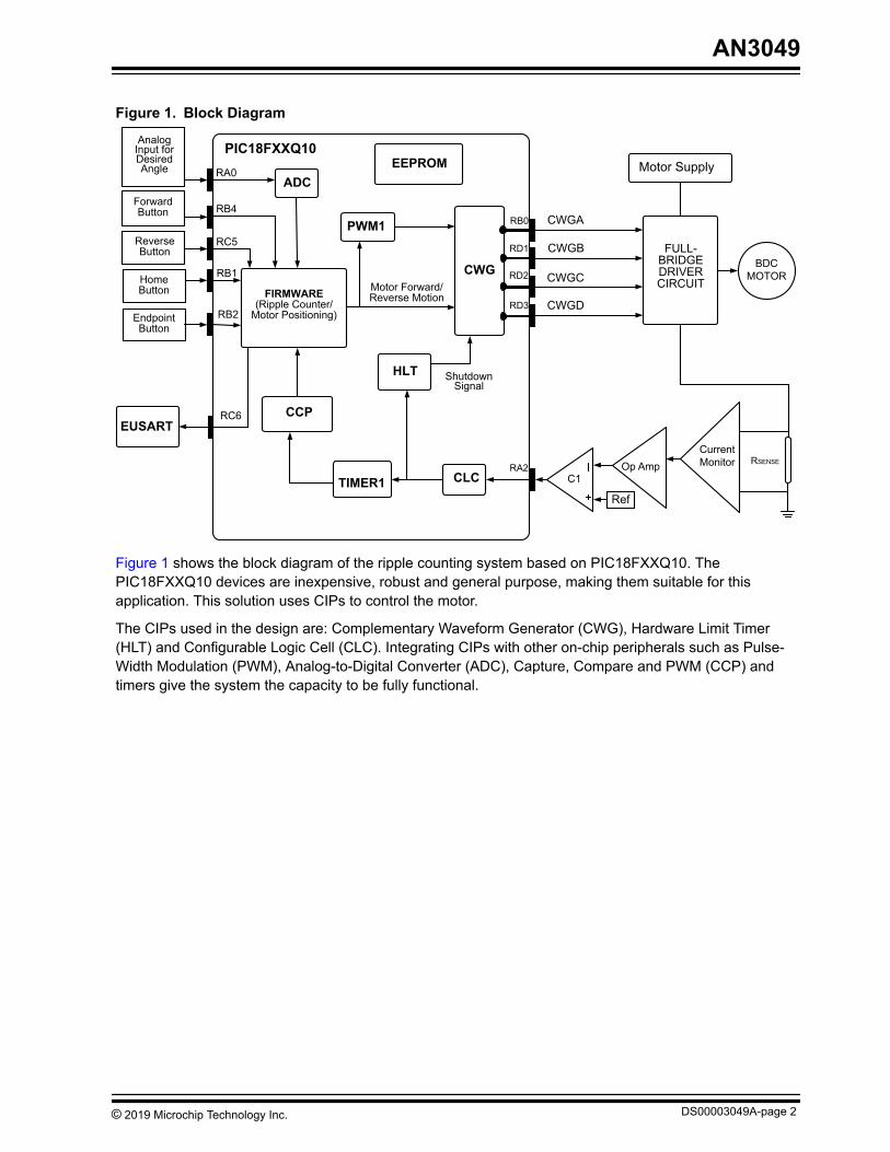
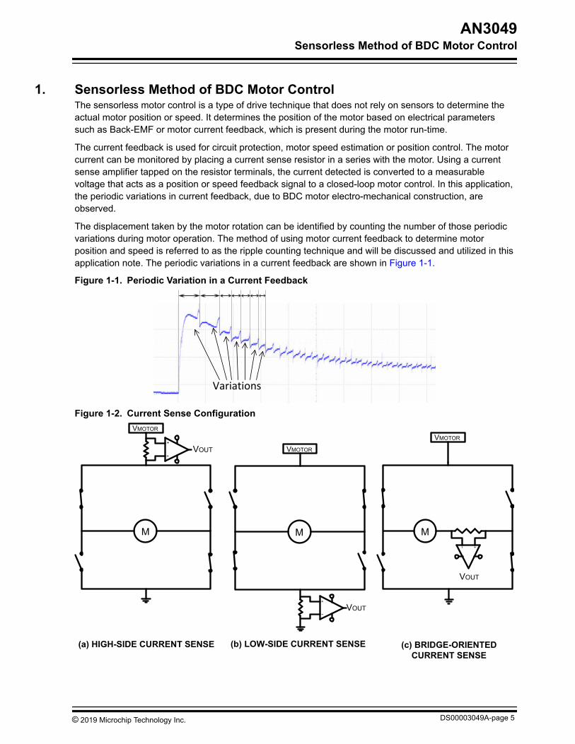
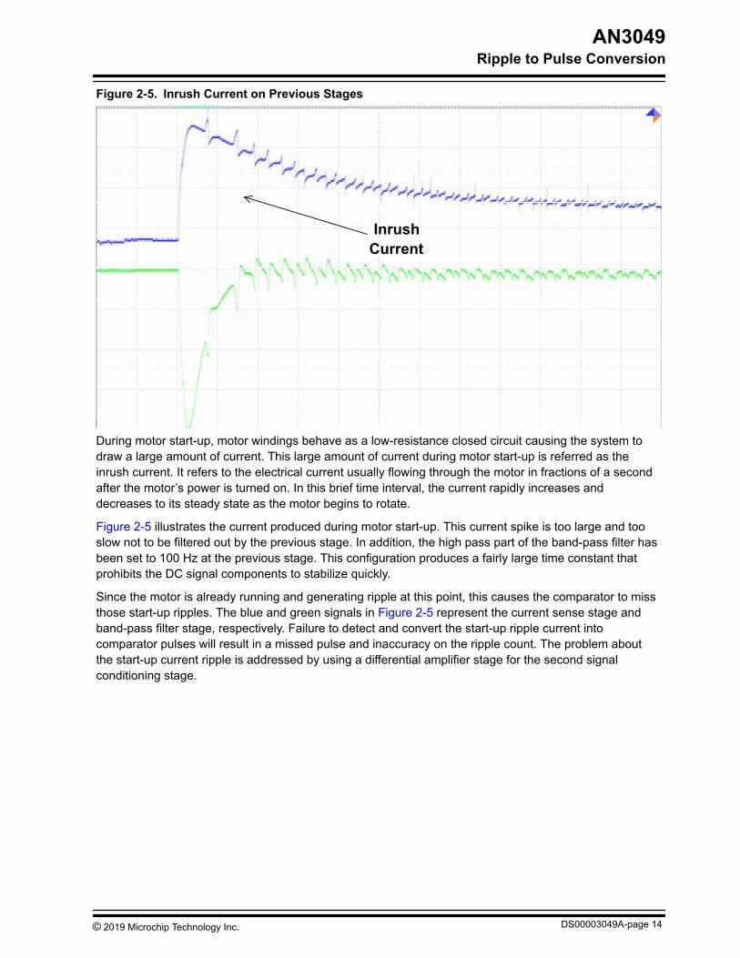
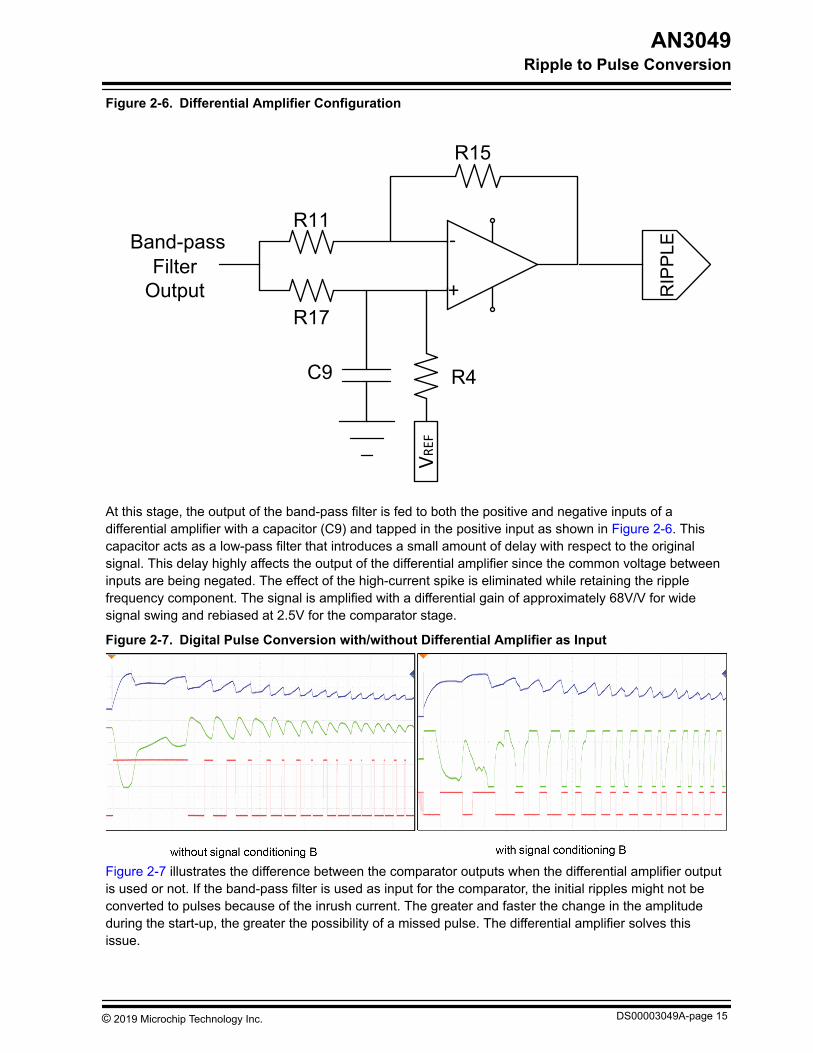
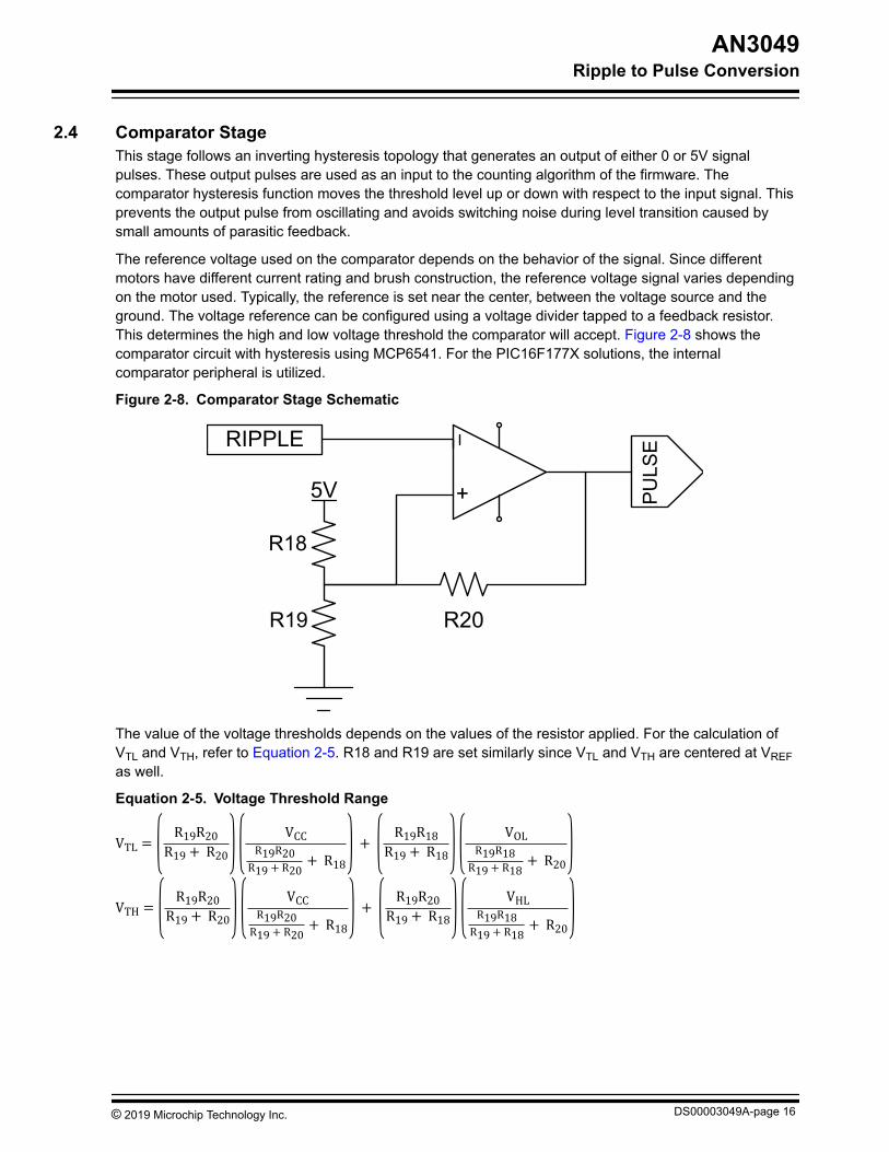
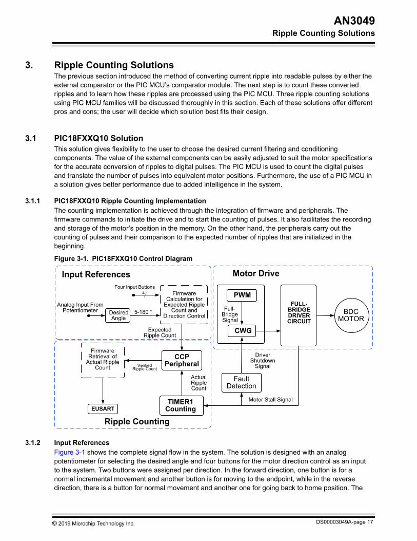
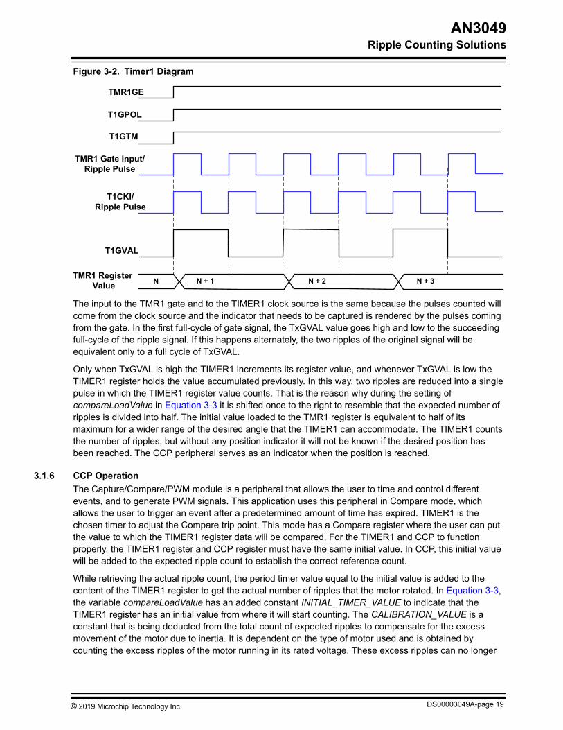
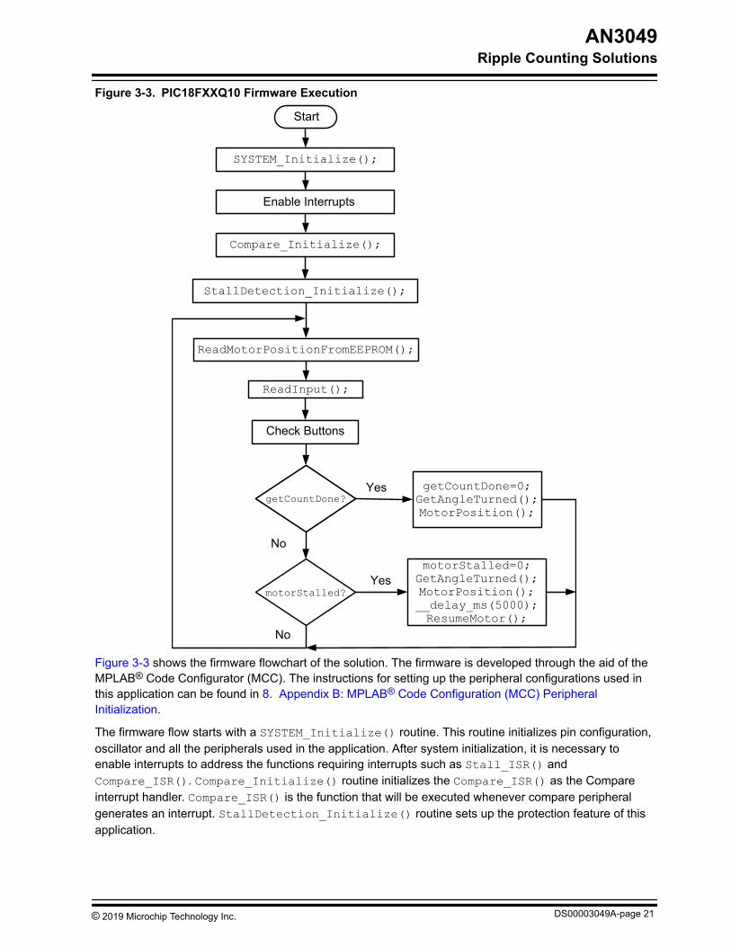
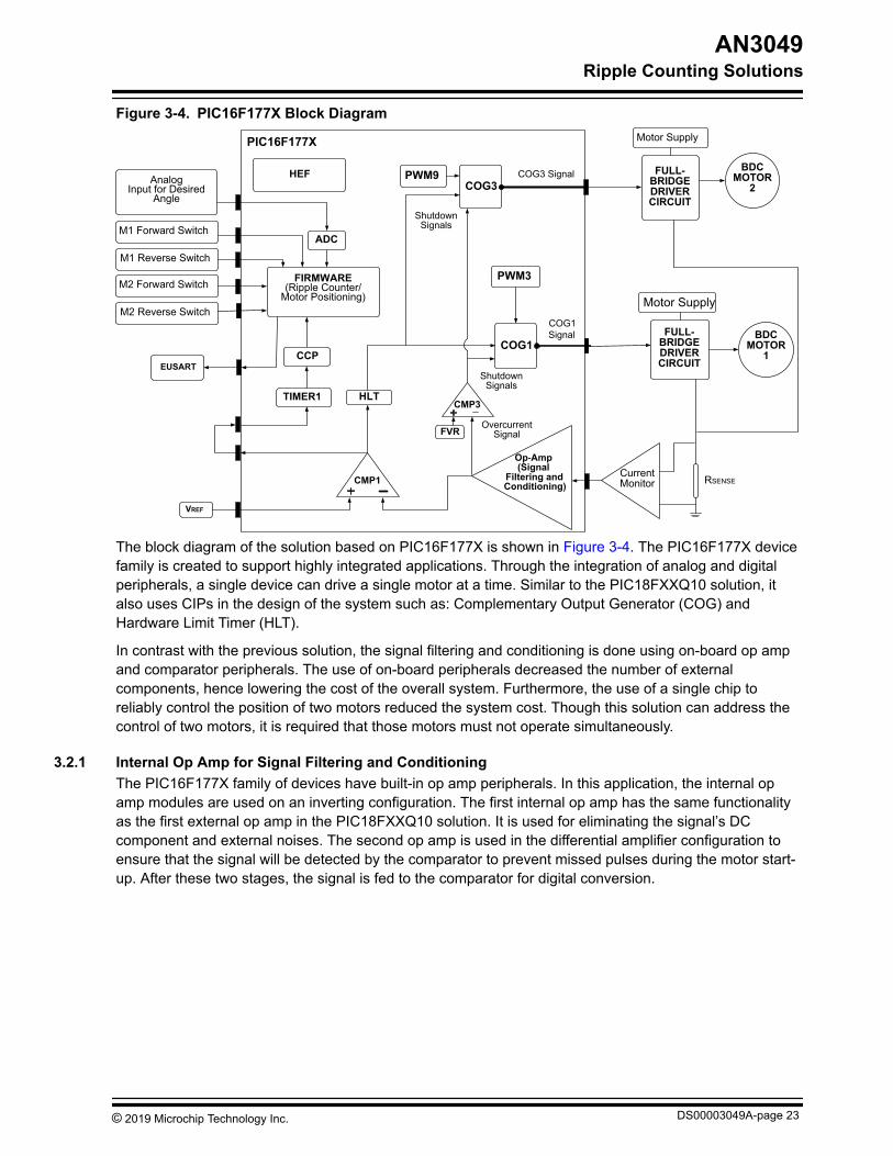
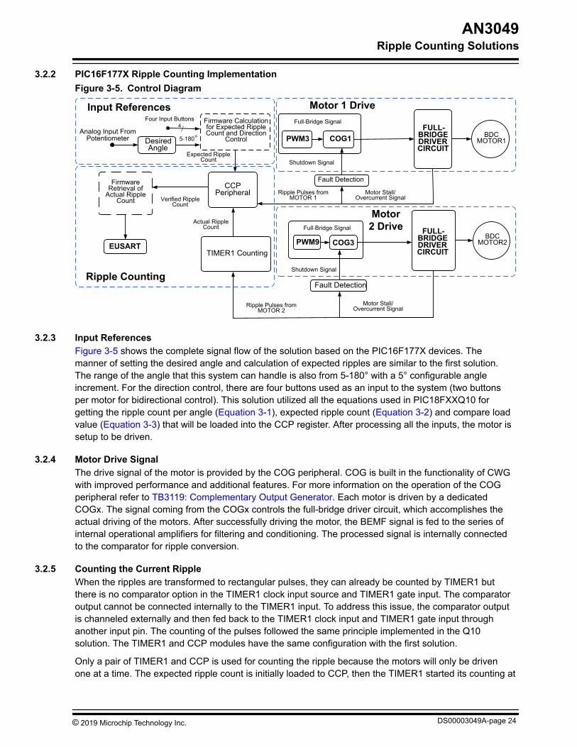
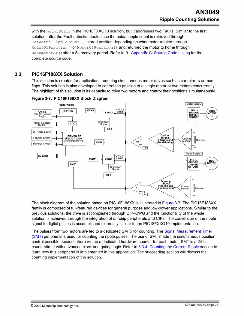
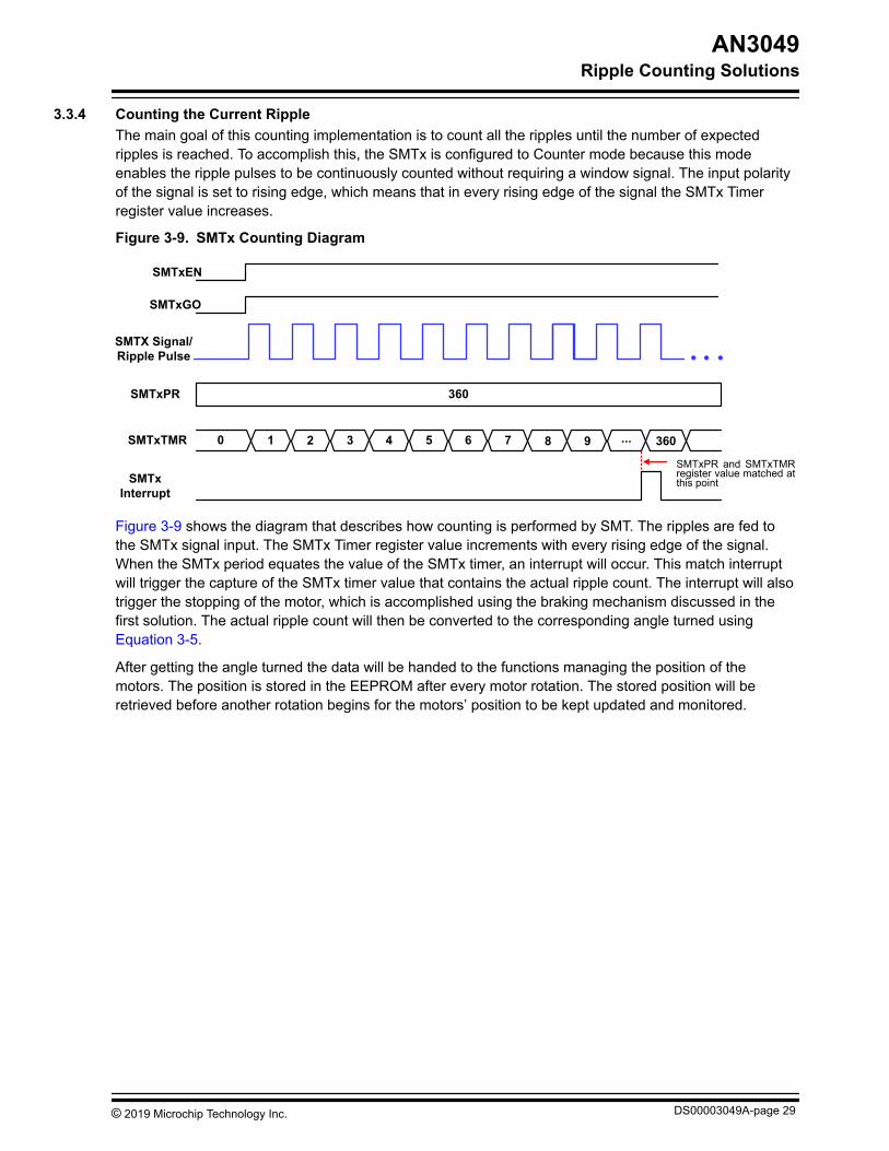
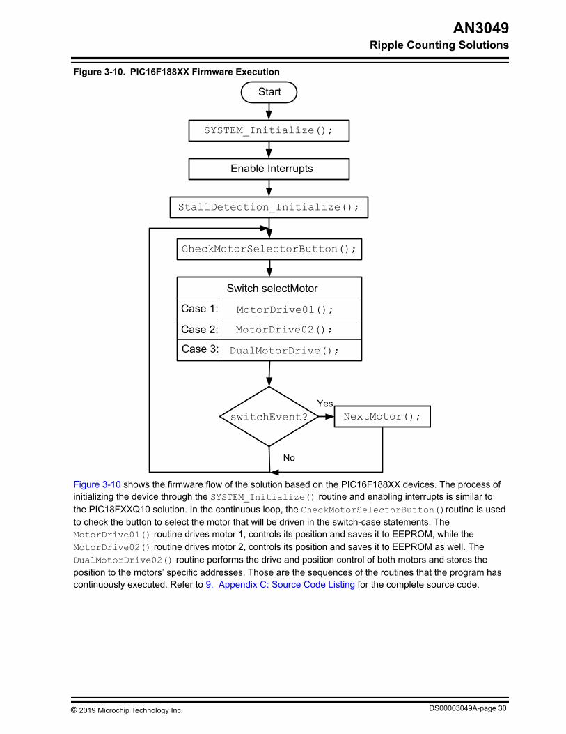
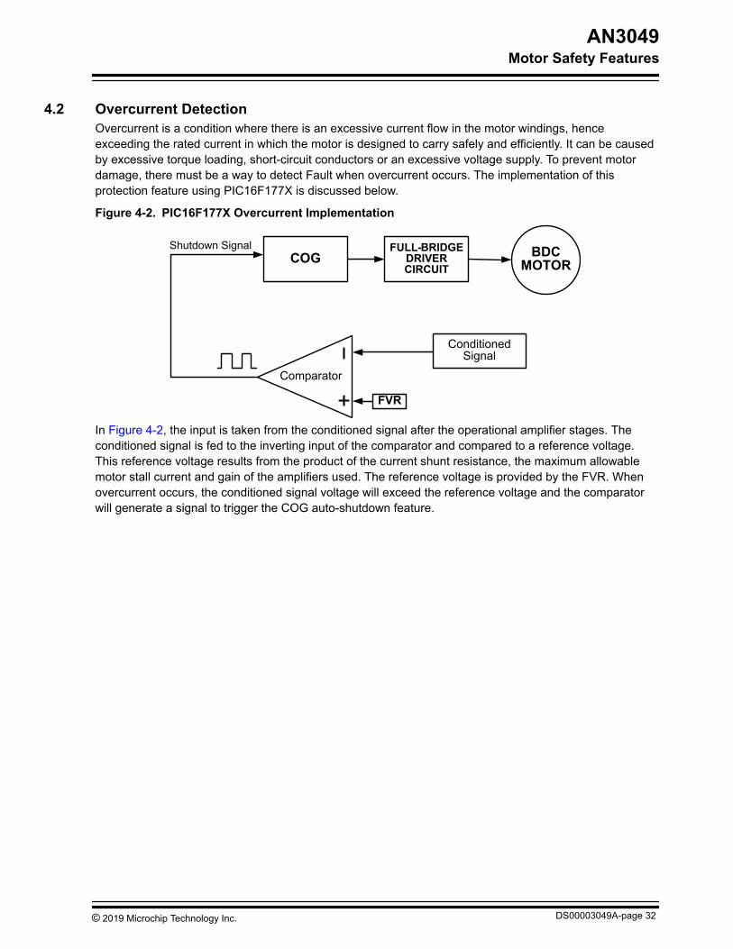
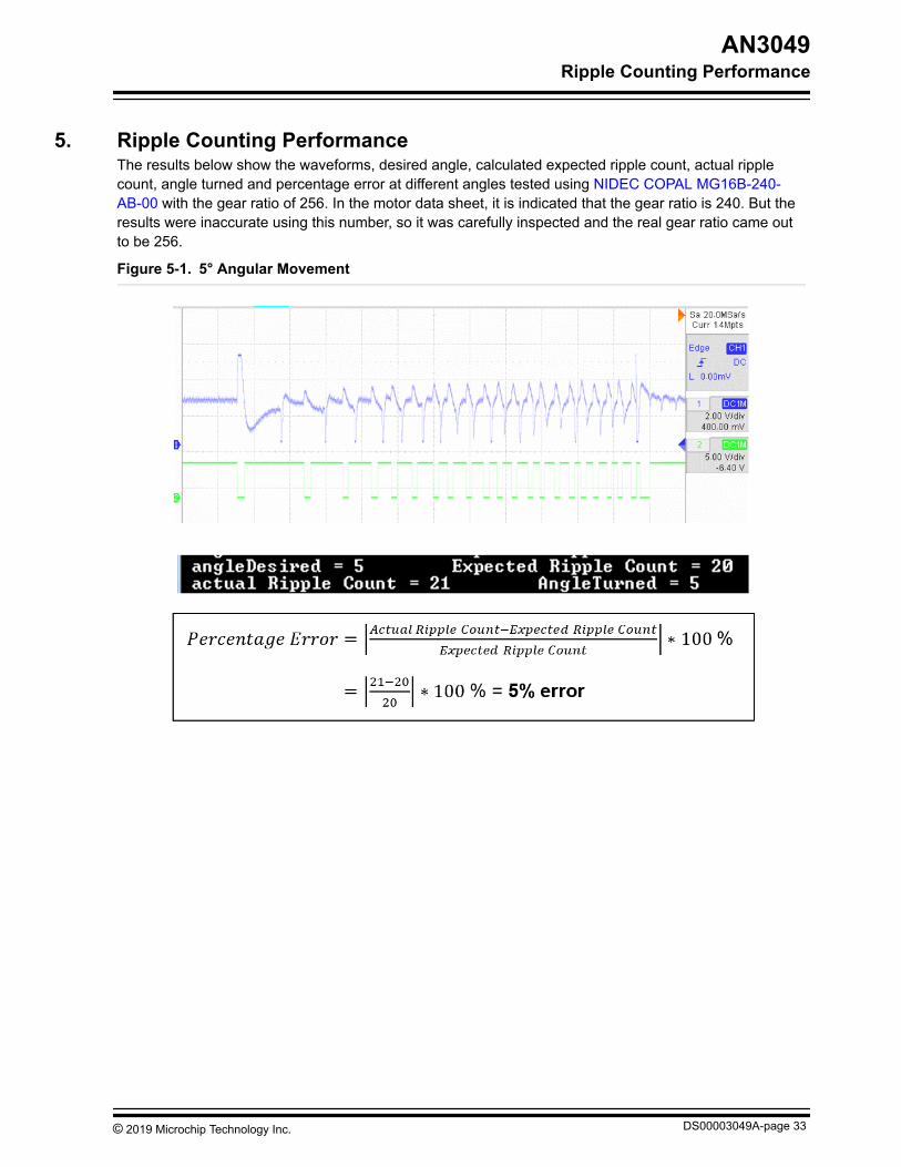
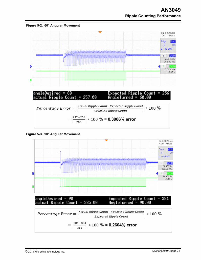
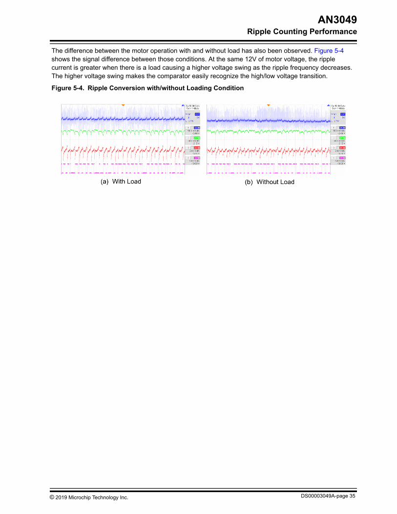
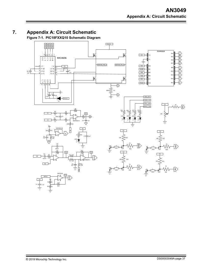
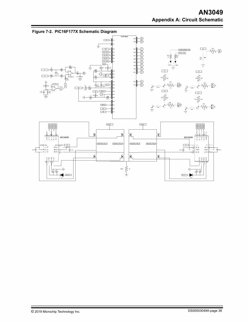
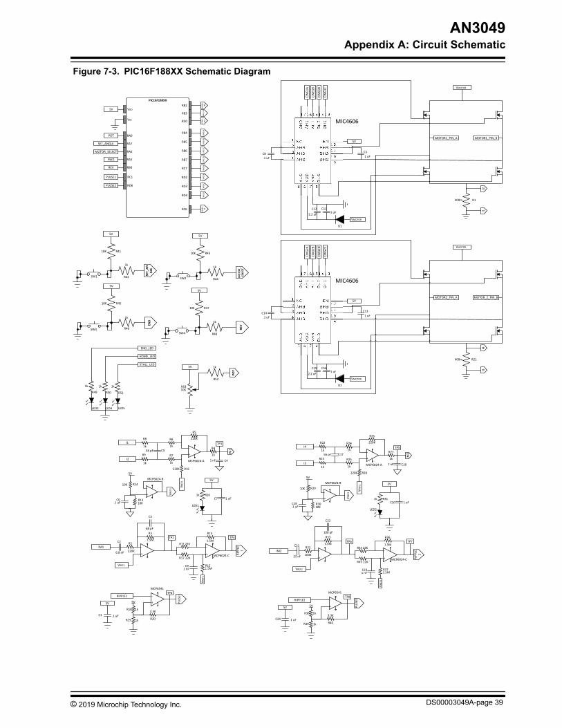
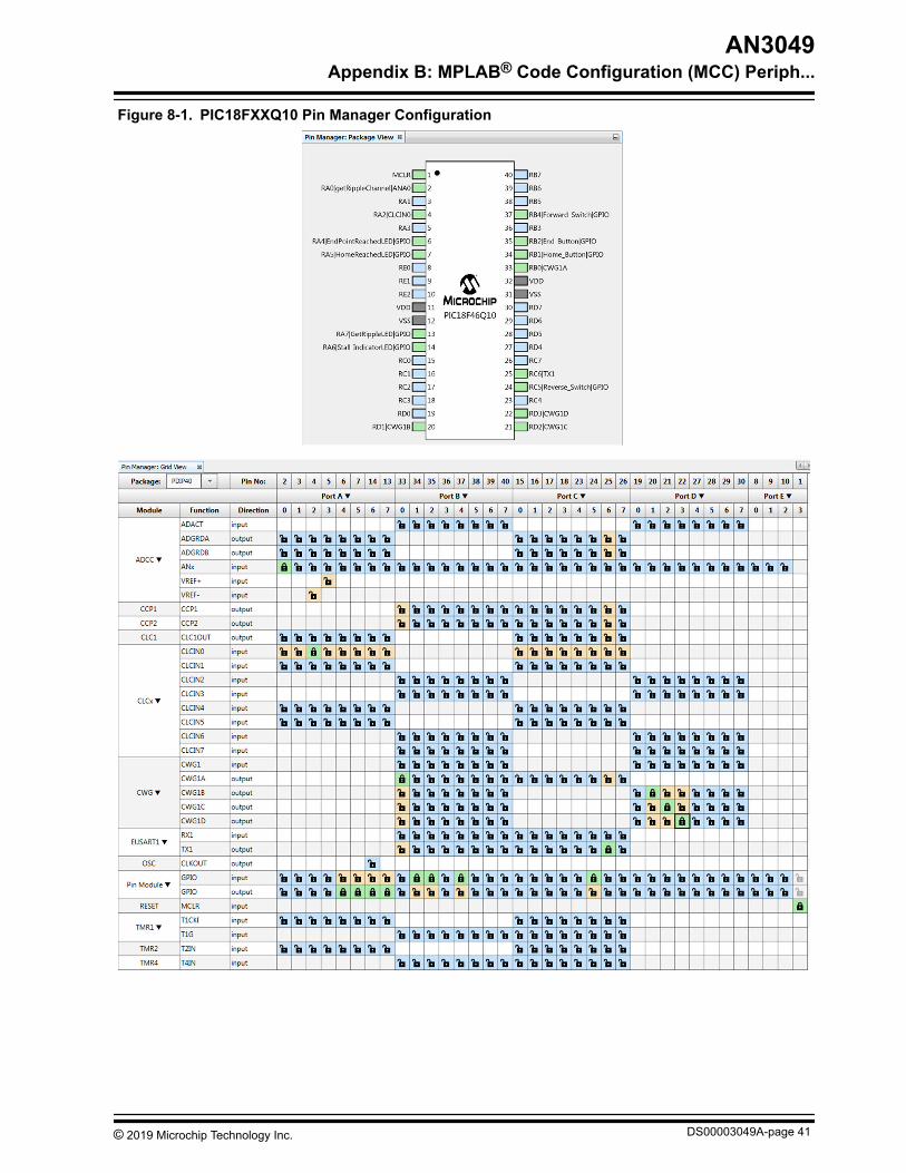
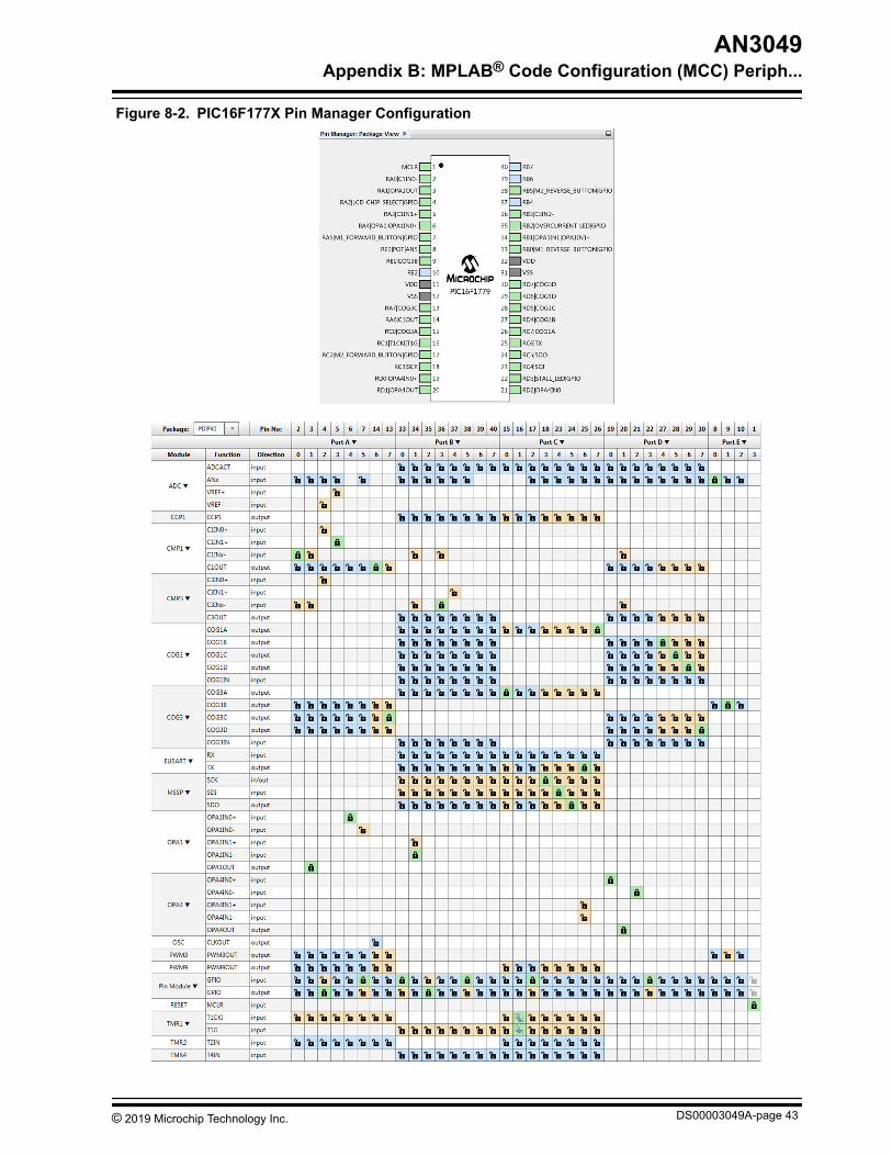