sensor and simulation notes note - university of new...
TRANSCRIPT

P!“ .,>t
Sensor and Simulation Notes
Note 410
September 1997CLEARED
W! PWLIC RELUSE
pL( Pflq &..97
Design of a Feed-Point Lens with Offset Inner Conductor
for a Half Reflector IRA with F/I) Greater than 0.25
W. Scott Bigelow
Everett G. Farr
Farr Research, Inc.
Abstract
An important component of a high-voltage half reflector impulse radiating antenna (HIM) is thefeed-point lens. Designs are available to feed reflectors which have focal length to diameterratios (F/D) equal to 0.25, but the theory for higher Ml ratios has not been available. Wedevelop here the theory for FD ratios larger than 0.25. We retain a rotationally symmetric lens;but the lens is now penetrated by an off-axis inner conductor. This conductor is offset such thatthe charge center follows a ray path, from the input feed, through the lens, which emerges at thespecific angle required to obtain the target FZDratio.

IF ““ -- FROM : F9RR RESERRCH PHONE NO. : 5135 293 3886 Sep. 29 1997 D2:19PM P2
FarrResearch614PaseoDclMar NEAlbuquerque,NM 87123phoneJfax (505) 293-3886
September29,1997
William D. PratherPhillips Laboratory /WSQ3550AberdeenAve. ,SEKirtlandAFB,NM 87117
DearMr.Prather,
I would like to submit for public release the attached Sensor and Simulation Note 410,entitled “Design of a Feed-Point Lens with Offset Inner Conductor for a Half Reflector IRA withF/D Greater than 0.25” There is no company proprietary data in this note.
If you have any questions, please do not hesitate to call me at the number above. Thank-you very much.
Sincerely,
Everett G. Farr, Ph.11

b
●
1. Introduction
Design equations were developed in [1] for the dielectric feed-point lens used to match an
electrically large coaxial waveguide to the feed arms of a high-voltage half reflector impulse ra-
diating antenna (HIRA). This lens converts a plane wave in the coaxial waveguide to a spherical
wave launched onto the conical feed arms of the antenna. In [2], the design equations were re-
fined by incorporation of an impedance matching condition between the input and output of the
lens. Since the problem could be solved semi-analytically only for a rotationally symmetric
geometry, a single conical feed and a 0.25 F“ (parabolic reflector focal length to diameter) ratio
were assumed. Here we extend that design approach to obtain an approximate solution for
HIRAs with feeds that break the rotational symmetry. This permits consideration of HIRAs with
ELD ratios larger than 0.25. As an example, we examine a high-voltage HIRA with an FZD ratio
of 0.40. Potential advantages of a larger Z?D ratio are reduced pre-pulse to impulse ratio in the
radiated field, and improved low-frequency performance.
In extending the design approach for HIRAs with rotationally symmetric feeds to those
with lVD greater than 0.25, the lens design remains rotationally symmetric; but the lens is pene-
trated by an off-axis inner feed conductor. Thus, in the region behind the lens, the charge center
is parallel to, but no longer coaxial with the
Lens
Transmission Line
I 1/1o11; I
1:11q
Offset from+ ‘+ Center Line
Figure 1. Concept for a HIRA with offsetinner conductor and rotation-ally symmetric feed-point lens.
outer conductor. Within and beyond the lens,
the inner conductor is bent and flared to match
the ray paths in those regions. Thus, at the
output of the lens, the geometry is that of a
bent cone over a ground plane. The concept is
illustrated here in Figure 1.
The lVD ratio of the reflector deter-
mines the angle that the charge center of the
output cone must make with the ground
plane-the bend angle of the charge center of
the cone [3 (14)]. This angle, in conjunction
with the desired output impedance, determines
the angle between the axis of the output cone
and the ground plane-the bend angle of the
cone axis [3 (15)]. In turn, the half angle of thea
2
. . .

.
●
o
output cone is determined by the bend angle and by the desired feed impedance [3 (16)]. The
equations governing the cone angles referenced here are introduced in the derivation that
follows.
Conforrnal mapping between the input transmission line and the aperture plane provides a
relationship between the F’ZDratio and the relative radial offset of the charge center from the axis
of the input transmission line [2 (A.2.7)]. Thus, both the bend angle and the relative offset are
established by the reflector FZD ratio. Impedance matching to the bent cone output determines
the relative conductor radii in the transmission line, and the peak electric field on the inner
conductor places lower limits on conductor dimensions [4 (4.1) and (4.5)].
By retaining the rotational symmetry of the lens, we implicitly assume that the rays
emerge from the quartic lens surface in a spherical wavefront. The inner conductor is offset such
that the charge center follows the ray path from the input transmission line through the lens,
which emerges at the specific angle required to obtain the target FZD ratio. The rays associated
with the inner conductor axis and surface also follow paths determined by the lens design. Al-
though the charge center ray exits the lens at the correct angle, we find that the other rays exit the
lens at angles slightly different from the intended ones.
In the material that follows, we derive the relationships between the FLD ratio of the re-
flector and the input transmission line geometry; and we show how the rotationally symmetric
lens is integrated into the offset feed design. We also present a HIRA design calculation for an
FZD ratio of 0.40, in which the transmission line and reflector feed are designed to an impedance
of 100 S2 in air.

4
.
2. Design of an Offset HIRA Feed
2.1 Relationship of Output Reflector and Input Transmission Line Feed Geometry
The design derivation for the offset transmission line and reflector feed for HIM with
F“ >0.25 most conveniently begins at the reflector output. The reflector is described by half Qf
a parabolic dish, sectioned through its axis. The cut edge and axis lie in the ground plane. We
assume the dish opens toward the positive x-direction. Its axis is the x-axis. The focus is at the
coordinate system origin, and the vertex is at x = –F.
Y()
—
yz = 4F(F +x)
\/----
2=0 /’/’////
/“
(
=
—
= 2F
—“x
Figure 2. Geometry of a bent monotone feed fora HIRA-with F/D >0.25.
Figure 2 shows the cross sec-
tion of the dish in the x–y plane. A
single conical feed arm (bent
monotone) extends from the origin
and intersects the edge of the
the elevation, yo, such that its
center forms angle ~ with the
plane. The aperture diameter
dish is given by D = 2yo. If
~d = FD, h follows from
geometry that [3 (14)]
[)PO=arctan 12fd-~(8fd)
dish at
charge
ground
of the
we let m
simple
(2.1)
The angle, B, between the cone axis
and the ground plane is obtained from
[3 (15)], as modified for a single cone
over a ground plane-the original ex-
pression was for a pair of cones sepa-
rated by a symmetry plane. Thus,
(2.2)p= 2arctan
[)
tan(po/2)
tanh(2z~)
Finally, the feed cone half angle, a, is m
4

1
.
● given by a similarly modified version of [3 (16)]
a = arcsin[1sin(~)
cosh(2z& )(2.3)
where the characteristic impedance is ~ =fgZ@ and ~ = 376.727 S2. Thus, fd=ZVD,alone ,.
determines ~. The other two cone angles, a and ~, are determined by both fdand fg.
The next step in the derivation is to relate the reflector focal length to aperture diameter
ratio, fd=FZD,to the radial offset of the charge” center in the input feed line. We use a result of
the conformal mapping presented in [2 (A.2.7)], which relates y (height) in the aperture plane to
Y (radial position) in the input feed,
(2.4)
where da is the radius of a parabolic dish with focus in the plane of the dish edge, the case for
●which f-J= 0.25; and ‘3?1is the radius of the outer conductor of the input feed line. This relation-
ship is valid in the z = O plane for y on a line between (xo, O, O) and (xo, yo, O), and for Y = –x on
the closed interval –Yl s xs O. Here, y. is the intersection, corresponding to the FD ratio of
interest, of the charge center with the parabola. Within the cylindrical transmission line, we let
‘PCcl be the corresponding offset of the charge center from the axis of the outer conductor. Then,
upon rearranging, (2.4) becomes
Y(-c~ = I–yO/da
Y~ l+yo/da
Since yo = D / 2 and da = 2F, we have yo / da = l/(4fd).Thus (2.5) becomes
Yccl = l-@fd)w~ 1+1/(4fd)
(2.5)
(2.6)
Like the charge center exit angle, A, we see that this ratio depends only on the assumed F~
ratio.
e Now that we have the ratio of the offset of the charge center to the transmission line
radius, Yccl / ‘I’l, we derive the remainder of the transmission line parameters.
5

●
1
2.2 Derivation of the Characteristic Parameters of the Offset Transmission Line.
●For a cylindrical transmission line feed with offset inner conductor, we have from [5 (6)],
the conformal transformation
$= jcoth(w/2) (2.?)
where w = u + jv and < = x + jy. This leads to the following complex map (Figure 3 on page 7),
where circles of constant u (equipotentials) and lines of constant v (electric field lines) are mutu-
ally orthogonal. Since dimensions in the complex map are normalized, the axes are in dimen-
sionless units of fld and yld, where d is the distance from the charge center to a virtual ground
plane. The surfaces of the inner and outer conductors are indicated in the figure at the u-contours,
u = Z@, and U = u], respective] y. Below, we show that these contours are determined by our
choices of~d and Z.C.
We continue our derivation with reference to the complex map introduced in Figure 3. If
we let ‘PObe the radius of the inner transmission line conductor, and if we let ‘PCco be the offsetof the charge center from the axis of the innerhave
(d +!PCCl)*
and
(d+ TCCO)2
We solve (2.8) for the ratio, d / ‘Pl, obtaining
conductor, then,
= d2 + y;
= d2+@
From [6 (3.5)] we have for the normalized ordinate
Y sinh u—=d cosh U – COSV
Now, at the top of the u = U1circle, v = O; and at the bottom, v = m.Thus
from [6 (3.1)] or [5 (17)], we
m(2.8)
(2.9)
yl,tOp = Sinhq ~d Yl,bottom = SiIlh U~
d cosh U1– 1 d cosh U1 + 1
(2.10)
(2.11)
(2.12) ●

1
.
y/d
1.5
1.25
1
0.75
0.5
0.25
~/d = jcoth(w/2)
W=u+jv
~=x+jy
f~=o.4, q=looQ +
normalized to the distancefrom the charge center
to the virtual ‘ound plane:
4)=3.13417
U1= 1.46634 ‘maginar’’xisfl :fi:ilReal Axis ~ L.!kwl.
Plane \.—-0.4 -0.2 0 0.2 0.4 x/d
Figure 3. Complex potential map of a cylindrical feed line with offset inner conductor. The
axes of the outer and inner conductors are separated by the distance, YB. On thismap, all dimensions are normalized to the distance, d, from the charge center tothe virtual ground plane. The equipotentials, U. and x are determined by the FA9
ratio and by the impedance, Zc.

and
Yl, top – Yl, bottom _ Z!f?l _ Sinh U1 sinh U1
d d cosh U1 -1 – cosh ul + 1
This can be simplified to obtaind
— = sinh U1Y~
from which we readily obtain UI. Sincefg = Au / Av = (u. – U1)f 2z, we obtain U. from
Uf’J= lq +2zfg
In a manner analogous to that used to obtain (2.14), we have
d—=sinh~W()
.
m(2.13)
(2.14)
(2.15)
(2.16)
Since we know d / ‘Pl from (2.10), we now have the ratio of the transmission line conductor radii!PO= d/T1
(2.17)~ d/T. ●
To obtain an expression for !Pcco / Y’l, we divide (2.9) by y?, take the square root, and solve
for Wcco / V1
IIYcco/Y1 = (d/Y1)2 + (To/T1)2 - d/Vi (2.18)
Since the axis of the inner conductor is at (x, y) = (O, d +Tcco) in the complex plane, and the
axis of the outer conductor is at (x, y) = (O, d + TCC1 ), the offset or separation of the inner con-
ductor axis from the outer conductor axis is obtained from
Y~/Yl = Yc(+q – Yccd% (2.19)
where Tccl / !P1 is calculated by (2.6), and Wcco / VI is obtained from (2.18). Since the radial
position of the outer conductor axis is taken to be W = O, we have that YB is also the radial coor-
dinate of the axis of the offset inner conductor.
The offset transmission line feed is completely specified in terms of three physical
parameters, !P1, the outer conductor radius, To, the inner conductor radius, and YB, the radial9
8

.
a offset of the axis of the inner conductor. At this point, we know how both of the other parameters
scale with Y?l.
2.3 Using the Peak Electric Field to Set Minimum Feed Line Dimensions
To complete the specification of the offset transmission line parameters, we need only
specify the radius of either conductor. In doing so, we want to keep the peak electric field in the
line below some maximum, as in [1 (5.2)] for the rotationally symmetric case. The peak field in
the offset feed line occurs on the surface of the inner conductor, on the side” nearest the outer
conductor. In the complex plane, this occurs at (x, y) = (O, d + Tcco – YPo). At this point, the x–
component of the electric field vanishes by symmetry; and, from [7 (4.4)], we have
Ey(x = o, y) = ~ :(X;O’Y)y=d+Ycco-Yo
where V. is the electrical potential on the inner conductor and from [7 (4.5)]
[11+ y/dU(X= O,y) = in
1- y/d
Thus, the derivative in (2.20) is just &(x= O,y)/~ = l/(d + y) + l/(d – y). At the hot spot
(34(X= o, y) 1 1
b+
y=d+Ycco ‘V() = 2d – (Y. – !PCco) W. – Ycco
(2.20)
(2.21)
(2.22)
By using Au = 2zfg and the result of (2.22) in
!vl,fin =v~
[
1 1
1(2.23)
2nfg Emu Y#P~ – Yccoplj Yopq – Yccoplj + Yc(-1/Yl – Y1/Yccl
(2.20), we obtain after some rearranging
where Emm = EY is the maximum field permissible at the hot spot, and Tl,tin is the minimum
permissible outer conductor radius for the stated values of E- and Vo. Any larger radius can be
chosen.
With W1 known, Wo is obtained from (2.17); and YB is obtained from (2.19). We turn
anow to design of a rotationally symmetric feed-point lens to integrate with the offset feed.
9

II
3. Design of a Rotationally Symmetric Lens for Use with an Offset Feed
3.1 Adaptation of the F/D= 0.25 Design Algorithm for Use with an Offset Feed
In [2], the lens design calculation for aY
Ground Plsn~
HIRA with a 0.25 FZD ratio was begun by
specifying the dielectric constants in the input Ouarllc Surlace
transmission line, in the lens region, and in the
output region beyond the feed-point lens.
Figure 4 depicts the lens design geometry and
identifies the significant design parameters. InY, Outer Conductor
addition to the dielectric constants, we specify ...”the output impedance, that of an upright mono- ‘“’
cone over a ground plane, and matching input ~
impedance of the coaxial feed line. The outer (-tl + tz) (-tl +t2 +~) (-/1 +e2+~+a) (tz)
feed conductor radius is chosen to be consis-
tent with a specified peak electric field con-
straint, and the lens radius at the ground plane
is chosen subject to the constraint that the lens
design equations are then solved numerically.
Figure 4. Lens design parameters.
have a non-zero thickness on-axis. The lens o
In this case, based on the WD ratio and on the input and
already determined the geometry of the offset feed and the exit
output impedance, Zc, we have
angle of the charge center. The
goal of our lens design is to cause a ray, which is injected parallel to the axis of the input feed
and at the radial location of the charge center, !PCC1, to exit the quartic surface of the lens at the
angle required by the FLDratio, ~. This will happen if we choose the center conductor radius for
the lens calculation, !PO,lens,equal to Y?ccl, and if we make &, the half angle of the output ray
monotone, equal to the complement of ~. We have appended the subscript “lens” to Y?O,as used
here, in order to avoid confusion with the radius of the offset inner conductor.
The lens design algorithm calculates ~ from the expression for the characteristic
impedance of a monotone over a ground plane [2 (2.8)] as
?90= 2arccot(K~) (3.1)
10

●
m where Kz = exp(2~ fg,monocone ) ‘exp[2zzC,monocone /ZO). Since, here we use @= 90° -~,
we simply calculate the constant, Kz, by inversion of (3.1), rather than basing it on impedance.
From this point, the lens design algorithm proceeds exactly as for the rotationally sym-
metric, F’ZD= 0.25, HIRA. We summarize that method here. Later, we present a sample design
calculation using this approach.
3.2 Lens Design Algorithm as Applied to a HIRA with Offset Feed
As described above, there are only minor adjustments required to adapt the lens design
approach described in [2] to the case of a rotationally symmetric lens used with an offset feed.
Three parameters normally established at the start of the design calculation are now determined
by a prior offset feed design calculation: (1) the exit ray monotone half angle, 00, is determined
by ~, the angle between the emerging charge center and the ground plane; (2) the inner con-
ductor radius, Wo,len~,is taken to be the radial coordinate of the offset charge center, Tccl; and
(3) the outer conductor radius for the offset feed, !PI, is also the outer conductor radius for the
lens design. A fourth parameter, the lens radius at the ground plane, W2, remains arbitrary, sub-
,
ject to the minimum required to ensure that the lens has non-zero thickness on axis, and that
electrical breakdown does not occur between the emerging offset feed and the ground plane.
We begin the design algorithm by numerically solving [2 (2.17)] for the conductor flare
angles, 81 and 60, as shown above in Figure 4,
(–csct?o+& Cotoo-xo+” JG) -1+6(-.,+42)\ ) \ )
r = (3.2)–cscoo+cot190-xo+& 1+X: r–l–xl+= 1+X;
where we have made the change of variable, xi = cot @i; and where, from [2 (2.18)], we have
X() = –Kz((2.1-2Gm)-(2xl-2Gm))
2(–l+&rJ (3.3)
(( J-))2 E,l – K; Erl–x:(l + @+2x& l+X?
11

i“
4
and Kz = cot(Oo/2), &rl = &2/&l, and &r2 =&2 /t33 . After using (3.3) to eliminate xo from
(3.2), we use Newton’s method to solve for xl = cot 81. Next, X. is obtained from (3.3); and 01 a
and f30 are recovered as arccot(xl ) and arccot(xo), respective y.
This completes the lens design, save specification of the output lens radius, T2. The
parameters of the ellipsoidal surface, a and d, are obtained from [2 (2. 11)] and [1 (3.2)] as -
~ _ 4%1– —(cot O1+Kcsc81)Y1 and c1 = a/~&rl– 1
The ratio, l?2/l?l, is obtained from [2 (2. 10)] as
Next, the ratio, Y?2/11 , is calculated from [2 (2. 19)] as
Y2 = l–/2//~
~ cot 81
Finally, from Figure 4 above, the thickness of the lens on axis
terms of lens thickness, we can write
Y2 = (to+a+d)~
(3.4)
(3.5)
(3.6)
o
is just, 40=/1 –(a +d). Thus, in
(3.7)
The minimum allowable lens output radius, ‘4’2,ti., occurs for lo= O.
Equation (3.7) can be used to determine the T2 required to produce any desired lens thickness, or
any value larger than Y-’2,tinmay be chosen, for example, to satisfy an electrical breakdown con-
straint. The design is completed by calculating 41 from the ratio produced by (3.6), and 12 from
the ratio generated by (3.5).
12

Sample Design Calculation for a HIRA with an Offset Feed and 0.40 F/.D Ratio
We apply the design approach just derived to the case of a 100 Q HIW4 driven by a
cylindrical transmission line with offset inner conductor. The impedance of the oil-filled trans-
mission line is 67 Q (100 Q in air). Thus, ~g = Zc / ~ = 1CKY376.727. We postulate a peak
driving voltage, Vo, of 2.6 MV, and a maximum permissible electric field in the transmission ,.
line, EM, of 2 MV/cm. Although we assume a single conical feed for the half reflector, in prac-
tice, this can be replaced by a pair of
equivalent 200 Q feed cones, as depicted
later in Figure 9 (below). Table I sum-
marizes the parameters that served as input
to the calculation of the offset feed line de-
sign. Table II lists the resulting feed line
dimensions.
The charge center output angle, ~,
the radius at the charge center in the input
mfeed, ‘FCcl, and the radius of the outer con-
ductor, T1, are then used in a lens design
calculation, as described above and in [2].
The lens design assumes that the transmiss-
ion line is filled with oil having a relative
dielectric constant of 2.2, while the lens is
assumed to have a relative dielectric con-
stant of 7.0. The maximum radius of the lens
was set to 13 cm.
—
Table I. Parameters used to calculate theoffset transmission line design.
Parameter Value Source
fdo.400000 Assumed
1% I 100.000 Q I Assumed I
V() I 2.6 MV I Assumed I1 1
Emax 2 MVlcm Assumed i
b 64.0108° I (2.1)
6 21.3671° 900–~
Yc(#3’, 0.230769 (2.6)
dPP1 2.05128 (2.10)
U1 1.46634 (2.14)1 1 I
Uo 3.13417 I (2.15)
1dlYn 1 11.4630 I (2.16) I
‘P#P, 0.178947 (2.17)
Tccdwl 0.00779062 (2.18)
Yl,fin 4.75229 cm (2.23)
Table II. Offset transmission line dimensions.
I Item I Parameter I Value I Source I
Radius of outer conductor VI 4.75 cm Chosen z ‘P1,ti~Radius of inner conductor Y() 0.849998 cm (YfJwl) !PIOffset of axis of inner YB 1.05915 cm (’Pcc#P#Pccdyl) WIconductor from axis of
I outer conductor I I I I
13

4
Table III summarizes both specified and calculated lens design parameters. For the lens
design, the ground plane is normal to the symmetry axis of the lens. The coordinate system ori- 0
gin, (z, ‘?) = (0,0), is at the intersection of the symmetry axis and ground plane. With the excep-
tion of !I’O,lcns,the parameter symbols used in the table are those detailed in [2] and identified
above in the lens design sketch (Figure 4). In Figure 5, a sketch based on the parameters listed
here is overlaid with the offset transmission line design results presented previously in Table II. .
Table III. Lens design parameters for use with an offset transmission line
feed for a FZD = 0.4 HIRA.
Coax dielectric constant El 2.20000 Assumed
Lens dielectric constant E2 7.00ooo Assumed
Output dielectric constant &3 1.m Assumed
Output ray cone angle t?~ 25.9892°
Charge center radius ‘O, lens 1.09615 cm Y(-C1
Outer conductor radius w~ 4.75000 cm Offset choiceLens radius at ground plane Y* 13.0000 cm Assumed, (3.7)
Calculated Values—
Impedance constant Kz 4.33334 cot(z90/2)
Charge center flare angle (30 7.10° (3.2)
Outer conductor flare angle (31 55.24° (3.2)
Ellipsoid semi-major axis length 5.737 cmEllipsoid focal length : 3.216 cm (3.4)Ellipsoid focal point to quartic t~ 12.058 cm Y*/(Y2//J
surface distanceQuartic surface location 42 3.036 cm (/2//Jt~
Lens thickness on-axis 10 3.105 cm I j,–+a
Interface Intersections
Ellipsoid<harge center (Z~,Y())~~n~ (-0.224 cm, Ray tracing1.096 cm)
~uter feed conductor—lens (z#PJ (-5.725 cm,4.750 cm) ‘ayT
Quartic+harge center (Z3,Y3) (3.097 cm,1.510 cm) .!5
14
,.,..—..,.....—- ... . ,- ..-.,. ... . . ...,... ,,..- , , , ,-,. ,, ..,-... ,,, .,,,,. ... .. .— , ,,,,,. , , . .,.,, , ,,, , ,,.-,,, ,.-,. ... , ,,.- , ,..,,., .,.—- ....—

1
Ground Plan
1
o~ = 90.0”
--- ----- .Y2=13.000cm
Outer Feed Conduct
. WI = 4.750cm /’,4 - ,’
/’
2 - Feed Conductof
----- ‘------ --,’
-.----- .- . ..-
-10 ~ -8 / -6 -4 -2Outer Feed AxIs
o 2 4Olfaet Inner
Feed Axis Axial Position (cm)
Figure 5. Offset transmission line with symmetric feed-point lens for a 100 Q halfreflector IRA with a 0.40 F’lD ratio.
An examination of the comparison of predicted and observed (based on ray tracing) feed
cone parameters presented below in Table IV reveals that the design developed here is approxi-
mate, since only the charge center exit ray angle, ~, agrees exactly with the theory. The apparent
or ray cone-based output impedance is calculated by inversion of (2.3) as
z~ ()sin ~ZC = ~ arccosh —
sin a(4.1)
15
*
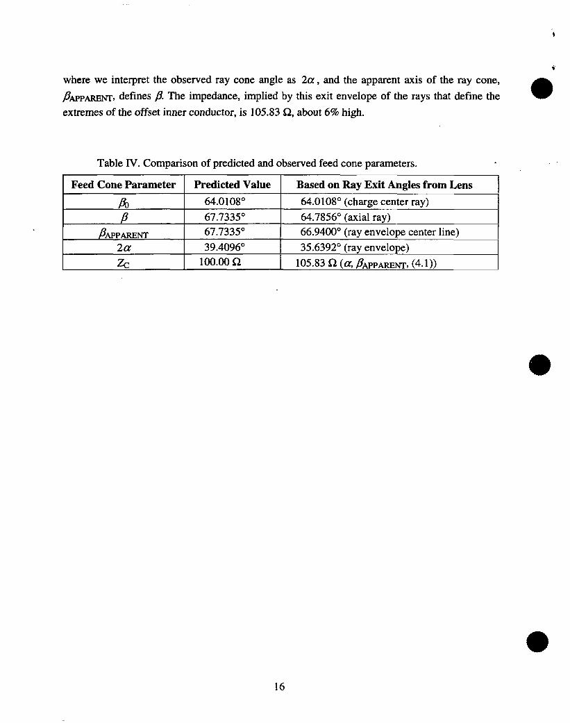
where we interpret the observed ray cone angle as 2a, and the apparent axis of the ray cone,
fl~pm~, defines fl The impedance, implied by this exit envelope of the rays that define the o
extremes of the offset inner conductor, is 105.83 f2, about 6% high.
Table IV. Comparison of predicted and observed feed cone parameters.
I Feed Cone Parameter I Predicted Value I Based on Ray Exit Angles from Lens,
I1
64.0108° 64.0108° (charge center ray)
P 67.7335° 64.7856° (axial ray)
APPARENT 67.7335° 66.9400° (ray envelope center line)
2a 39.4096° 35.6392° (ray envelope)
Zc 100.00 Q 105.83 Q (a, ~wpmm, (4. 1))
16

t
● 5. Discussion of the Results of the Sample Offset HIRA Design Calculation
To explore the deviations between our predicted and “observed” ray tracing results
(Table IV, above), we next consider the differing functional forms of the electrical potential
within the feed-point lens system. Three regions may be identified: (1) the oil-filled coaxial input
region, (2) the biconic lens region, and (3) the monotone-over-ground plane output region. For a
plane wave propagating in the axial (z) direction within the coaxial region, a ray initially at the
radial coordinate, W = %’C(the coaxial insertion radius), where a <WC e b (Figure 6), follows an
equipotential within each region. However, except at the surfaces of the conductors, the geomet-
rically traced ray follows a different equipotential within each region.
We now develop expressions for the poten-
tial function in each region and calculate the extent
of the shifts in potential identified above. First, in
the input coaxial region, we need the potential as a afunction of the cylindrical radius, Y. The potential
e on the center conductor is V = Vo; on the outer con-
ductor, it is V= O. Thus, between the conductors,\=vo@-a)
the potential as a function of radius is given by
v(Y) = V()in (!P/b)
in (a/b)
Figure 6. Coaxial geometry.(5.1)
Next, for the biconic lens region, we implement a stereographic projection in the direction of the
axis. The result is another coaxial geometry. In the following set of equations for the projection,
note that the parameter, Ro, is arbi-
~;lb
w
213a
=V=vo ;
v =0______._. _.i. _ . _ ._ ._ ._ .-.
trary.
T =2% tan(@/2)
Ta = 2% t~ (@a/2) (5.2)
Yb = 2% t@b/2)
Figure 7. Stereographic projection of a pair ofcoaxial cones joined at the vertex leadsto a coaxial cylindrical geometry.
17

. .-..=
Now, from (5.1) and (5.2), the potential
v(Y)
of the
= v~
projected structure
[)~n tan(o/2)
tan(8b/2)
[)
~n tan(ea/2)
tan((?b/2)
is
(5.3)
This expression is applicable to the region interior to the lens, where the flare .of the outer con-
ductor forms the outer cone and the flare of the center conductor forms the inner cone. Outside
the lens, the geometry is that of an upright monotone over a ground plane. Here, 6b + 90°; and
(5.3) reduces to
v(Y) = v~ln(tan(8/2))
ln(tan(8a/2))(5.4)
The normalized voltage functions, V(Y)/ Vo,for input coaxial, lens biconic, and output
monotone regions, as functions of the coaxial insertion radius, !Pc, were computed for the lens
1
0.8
0.2
0
2 4 6 8 10Insertion Radius (cm)
Figure 8. Relative potentials for a rotationally symm-etric feed-point lens design. The potentialsare shown within the input feed (coaxial re-gion), within the lens (bicone region), and atthe lens output (monotone region), as func-tions of the coaxial insertion radius.
designed in the preceding exam-
ple. The results are presented in
Figure 8. These results indicate●
that all rays, except those at
the conductor surfaces, expe-
rience a different potential within
each region. The magnitude of
the potential shift at each inter-
face is a function of insertion ra-
dius. The three curves in the
figure give the relative potential
as functions of the radial coordi-
nate at insertion: for the coaxial
insertion region, for the lens re-
gion, and for the lens output re-
gion. If our design theory were
exact, these three curves would
overlap perfectly; and every inserted ray would remain on the same equipotential as it is ray-
traced through the structure.
18
r
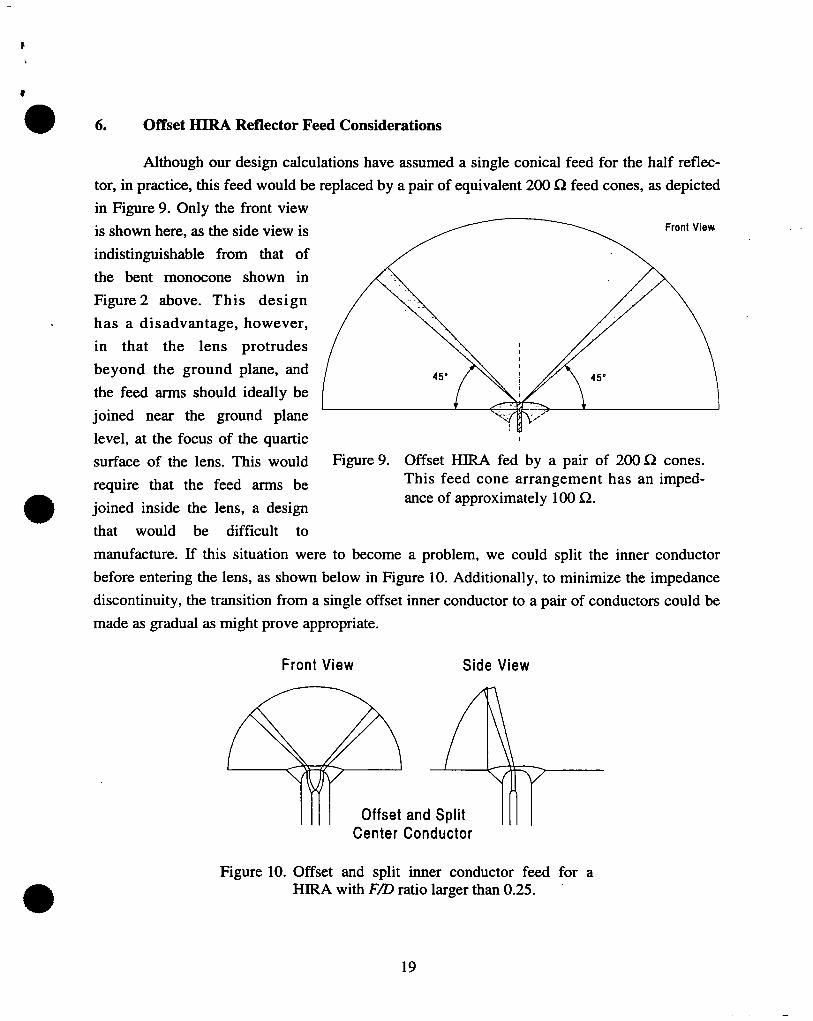
● 6. Offset HIRA Reflector Feed Considerations
Although our design calculations have assumed a single conical feed for the half reflec-
tor, in practice, this feed would be replaced by a pair of equivalent 200 Q feed cones, as depicted
in Figure 9. Only the front view
is shown here, as the side view is
indistinguishable from that of
the bent monotone shown in
Figure 2 above. This design
has a disadvantage, however,
in that the lens protrudes
beyond the ground plane, and
the feed arms should ideally be
joined near the ground plane
level, at the focus of the quartic
surface of the lens. This would
require that the feed arms be
e joined inside the lens, a design
that would be difficult to
Front View
Figure 9. Offset HIRA fed by a pair of 200 Q cones.This feed cone arrangement has an imped-ance of approximately 100 Q.
manufacture. If this situation were to become a problem, we could split the inner conductor
before entering the lens, as shown below in Figure 10. Additionally, to minimize the impedance
discontinuity, the transition from a single offset inner conductor to a pair of conductors could be
made as gradual as might prove appropriate.
Front View Side View
Offset and SplitCenter Conductor
Figure 10. Offset and split inner conductor feed for aHIRA with IVD ratio larger than 0.25.
19

7. Concluding Remarks
We have provided a design approach for the feed-point lens and offset cylindrical feed
line needed to build a high-voltage half IRA with an HD ratio larger than 0.25. For the example
with an FZ!l ratio of 0.40, the ray paths through the lens at the offset feed location are not quite
correct. However, the impedance based on these rays is only slightly different from the design
target. This difference may be related to the shifts in potential experienced by rays traversing the
feed-point lens system. It seems unlikely that a significant impact on measurable HIRA
performance can be expected to result from the approximate nature of this design approach.
Acknowledgments
We would like to thank Mr. William D. Prather of Phillips Laborato~ for funding this work. Wewould also like to thank Dr. Carl E. Baum for his many helpt%l discussions that contributed tothis effort.
References
1.
2.
3.
4.
5.
6.
7.
E. G. Farr and C. E. Baum, Feed-Point Lenses for Half Reflector IllAs, Sensor and mSimulation Note 385, November 1995.
W. S. Bigelow, E. G. Farr, and G. D. Sower, Design Optimization of Feed-Point Lenses for
Half Reflector IRAs, Sensor and Simulation Note 400, August 1996.
E. G. Farr and C. E. Baum, Prepulse Associated with the TEM Feed of an Impulse Radiating
Antenna, Sensor and Simulation Note 337, March 1992.
E. G. Farr, G. D. Sower, and C. J. Buchenauer, Design Considerations for Ultra-Wideband,
High-Voltage Baluns, Sensor and Simulation Note 371, October 1994.
C. E. Baum, Impedances and Field distributions for Symmetrical Two Wire and Four Wire
Transmission Line Simulators, Sensor and Simulation Note XXVII, 10 October 1966.
E. G. Farr, Optimizing the Feed Impedance of Impulse Radiating Antennas, Part I, Reflector
IRAs, Sensor and Simulation Note 354, January 1993.
E. G. Farr and G. D. Sower, Design Principles of Half Impulse Radiating Antennas, Sensor
and Simulation Note 390, December 1995. m
20