sem operation - hebrew university of jerusalemchem.ch.huji.ac.il/~porath/nst2/lecture 2b.pdf · sem...
TRANSCRIPT


SEM Operation
Magnification = length of TV screen/Scanning length

SEM Operation
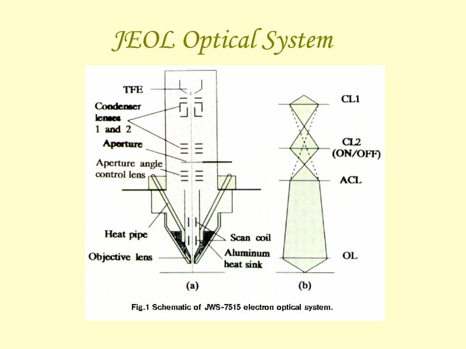
JEOL Optical System

SEM Ray DiagramsLarge WD:
• Demagnification decreases
• Spot size increases
• Divergence angle α decreased
The decrease in demagnification is obtained when the lens current is decreased, which in turn increases the focal length f of the lens. The resolution of the specimen is decreased with an increased working distance, because the spot size is increased. Conversely, the depth of field is increased with an increased working distance, because the divergence angle is smaller.
Small WD Large WD

Beam's Path through the Column

Light vs. Electron Microscopes

The Electron SourceThe electron source:
Filament: Tungsten
This filament is a loop of tungsten which functions as the cathode. A voltage is applied to the loop, causing it to heat up. The anode, which is positive with respect to the filament, forms powerful attractive forces for electrons.
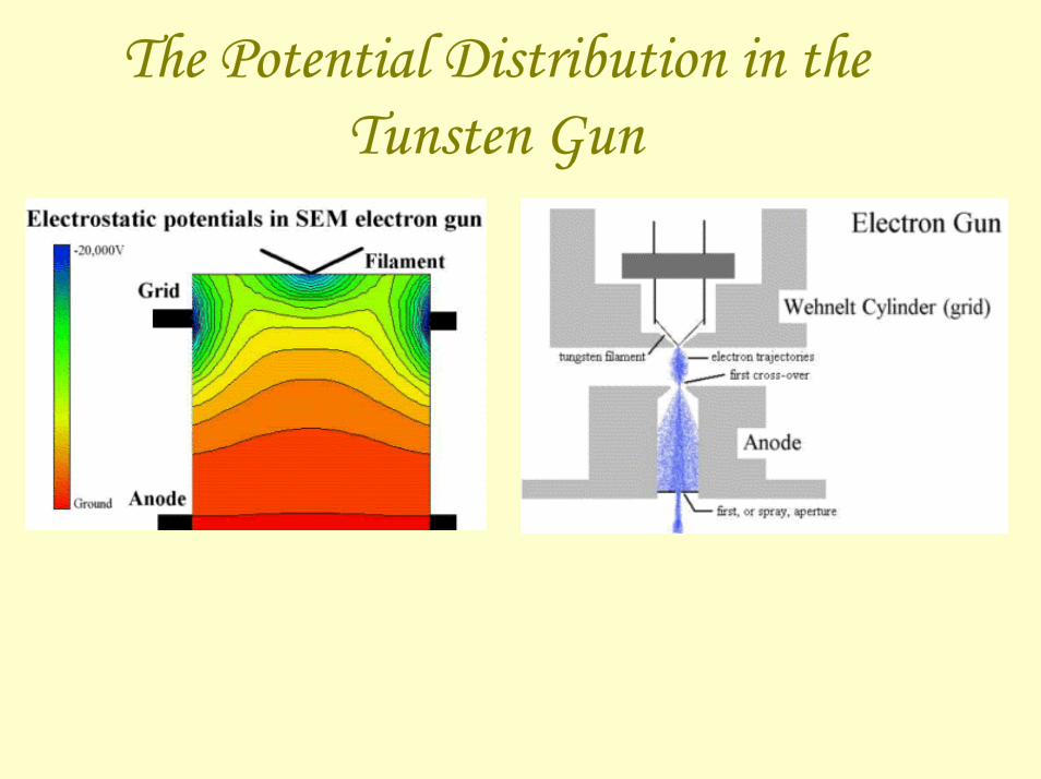
The Potential Distribution in the Tunsten Gun

LaB6 Gun

Field Emission Gun

Field Emission Gun

Gun TypesSEM Cathode Comparison
Tungsten filament LaB6
Schottky(TF)
Field Emission
Apparent Source Size 100 micrometers
5 micromete
rs
<100 Angstroms
<100 Angstroms
Brightness 1 A/cm2
steradian
20-50 A/cm2
steradian
100-500 A/cm2
steradian
100-1000 A/cm2
steradian
Vacuum Required10-5 Torr 10-6 Torr 10-8 Torr 10-9 Torr

Thermionic Emitter Materials

JEOL Probe Current Control
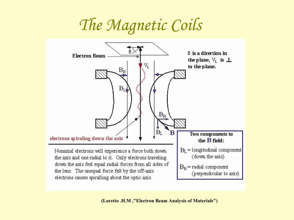
The Magnetic Coils
( )"Electron Beam Analysis of Materials" ,M.H .Loretto

The Magnetic Lenses
( )“ ???

The Scanning Coils
Scan the sample (raster)
Synchronized with CRT
One pair of coils for X and one for Y

JEOL Heat Conductive System –TO Avoid Thermal Drift


Collected Signals in SEM
Sample
Secondary electrons (SE)
Backscattered electrons (BSE)
Cathodoluminescence(CL)
X-rays
Absorbed current
Incident beam
Courtesy Z. Barkay

Information from Electron Beam-Specimen Interactions
While all these signals are present in the SEM, not all of them are detected and used for information. The signals most commonly used are theSecondary Electrons, the Backscattered Electrons and X-rays
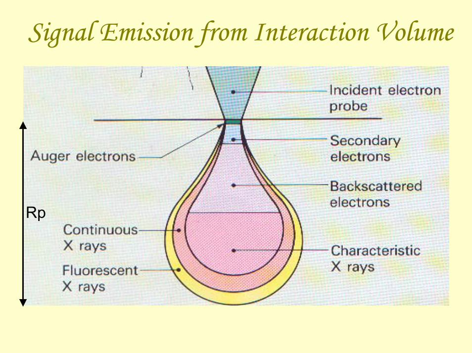
Signal Emission from Interaction Volume
Rp

Basic SEM Modes of Operation - SummarySignal/Mode Information Material Resolution Secondary
electrons (SE) Morphology All (*) ~1nm
Backscattered electrons (BSE)
Atomic number
All (*) 0.1-0.5µm(**)
X-ray (EDS or WDS)
Atomic composition
All (flat) ~1µm
(CL)Cathodo- luminescence
Bandgap, impurities, lifetimes
Insulators and semi- conductors
~ 1µm
(*) usually sizes of 1cm, dependent on SEM configuration
(**) voltage and Z dependent
Additional modes: Voltage contrast (VC) and EBIC - usually used in devices and p-n junctions. Courtesy Z. Barkay

Inelastic Scattering
During inelastic scattering, energy is transferred to the electrons surrounding the atoms and the kinetic energy of the
can transfer a various amount of energy from the beam electron ranging from a fraction to many kilo-electron volts. The main processes include phonon excitation, plasmon excitation, secondary electron excitation, continuum X-ray generation, and ionization of inner shells. In all processes of inelastic scattering, energy is lost, though different processeslose energy at varying rates.
energetic electron involved decreases. A single inelastic event

Secondary Electrons
1. Secondary electrons are predominantly produced by the interactions between energetic beam electrons and weakly bonded conduction-band electrons in metals or the valence electrons of insulators and semiconductors.
2. There is a great difference between the amount of energy contained by beam electrons compared to the specimen electrons and because of this, only a small amount of kinetic energy can be transferred to the secondary electrons.

Secondary Electrons and DetectionSE are specimen electrons that obtain energy by inelasticcollisions with beam electrons.
emitted from the specimen with energy less than 50 eV
A broken surface of a piece of metal, formed using SEimaging
They are defined as electrons

The origin of high SE spatial resolution
•High resolution SE(1): 1 nm•Lower resolution SE(2): 0.1-1 µm
Courtesy Z. Barkay

Elastic Scattering – Backscattering
As the name implies, elastic scattering results in little (<1eV) or no change in energy of the scattered electron, although there is a change in momentum. Since momentum, p=mv, and m doesn't change, the direction of the velocity vector must change. The angle of scattering can range from 0-180 degrees, with a typical value being about 5 degrees.
Elastic scattering occurs between the negative electron and the positive nucleus. This is essentially Rutherford scattering. Sometimes the angle is such that the electron comes back out of the sample. These are backscattered electrons.

Backscattering Detector
Elastic scattering occurs between the negative electron and the positive nucleus. This is
scattering. Sometimes the angle is such that the electron comes back out of the sample. These are backscattered electrons.
Aluminum copper alloy formed using backscattered electron imaging.
The light area is mostly aluminum and the dark area is mostly copper
essentially Rutherford

Energy distribution of SE and BSE
Courtesy Z. Barkay

DetectionAn electron detector is used with the SEM to convert the radiation of interest into an electrical signal for manipulation and display by signal processing electronics, which is much
Thornley (E-T) detector. It works in the following manner:
The scintillator material is struck by an energetic electron. This collision produces photons which are conducted by total internal reflection in a light guide to a photomultiplier. These photons are now in the form of light so they can pass through a vacuum environment and a quartz glass window. The photon is then converted back into an electron current where a positive bias can attract the electrons and collect them so that they will be detected.
like a television. Most SEM's are equipped with an Everhart-
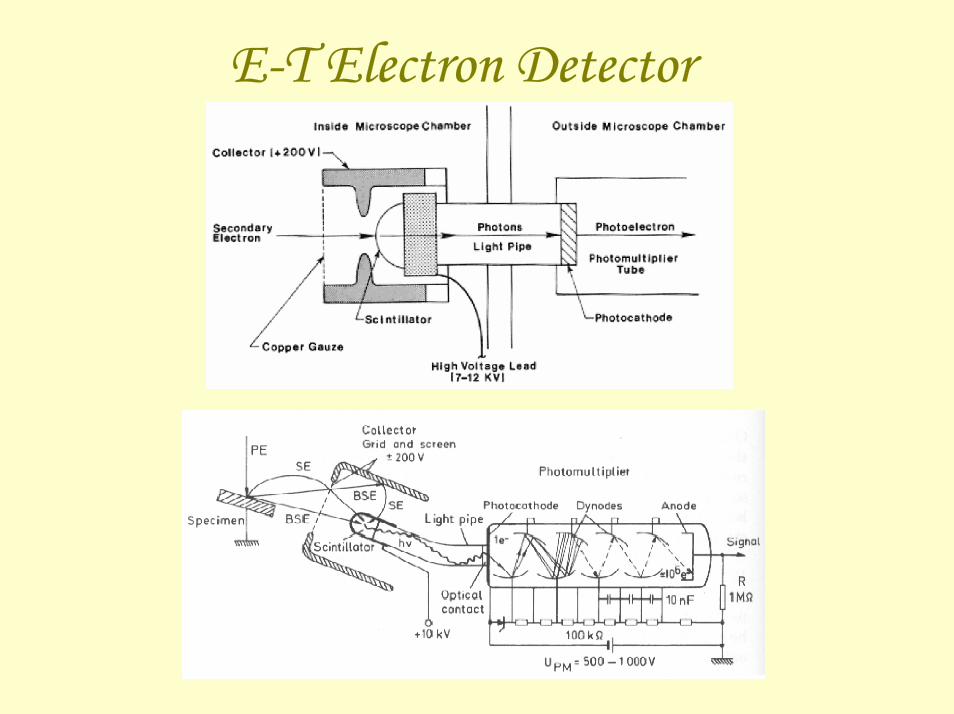
E-T Electron Detector

Vacuum
When a SEM is used, the column must always be at a vacuum. There are many reasons for this. If the sample is in a gas filled environment, an electron beam cannot be generated or maintained because of a high instability in the beam. Gases could react with the electron source, causing it to burn out, or cause electrons in the beam to ionize, which produces random discharges and leads to instability in the beam. The transmission of the beam through the electron optic column would also be hindered by the presence of other molecules. Those other molecules, which could come from the sample or the microscope itself, could form compounds and condense on the sample. This would lower the contrast and obscure detail in the image.
A vacuum environment is also necessary in part of the sample preparation. One such example is the sputter coater. If the chamber isn't at vacuum before the sample is coated, gas molecules would get in the way of the argon and gold. This could lead to uneven coating, or no coating at all.

The Objective Lens
Objective lens
SE detector
BSE detector
The lens that focuses the beam of electrons towards the sample.
The SE detector produces a clear and focused topographical image of the sample.
The BSE detector is used to determine the composition of the sample. Each element in the sample appears as a different shade, from almost white to black.

The Sample Chamber
The left photo shows the sample chamber located at the base of the column. The right photo shows the lens and detectors located inside the sample chamber.

The Stage
A prepared sample is mounted on a specimen stub and placed on the stage.

The Sputter Coater
The sputter coater is used to coat non-metallic samples (bugs, plants, human hair, etc.) with a thin layer of gold. This makes them conductive, and ready to be viewed by the SEM. If the samples are metallic, they can simply be mounted and placed in the SEM

Environmental SEM
ESEM enables to view specimens and processes in their natural state in a gaseous environment.

How Does ESEM Work?The primary electron beam hits the specimen which causes the specimen to emit secondary electrons. The electrons are attracted to the positively charged detector electrode. As they travel through the gaseous environment, collisions occur between an electron and a gas particle results in emission of more electrons and ionization of the gas molecules. This increase in the amount of electrons effectively amplifies the original secondary electron signal. The positively charged gas ions are attracted to the negatively biased specimen and offset charging takes effect.
As the number of secondary electrons varies the amplification effect of the gas varies. If a large number of electrons are emitted from a position on the specimen during a scan, there is a high signal. If only a small amount of electrons are emitted the signal is less intense. The difference in signal intensity from different locations on the specimen allows an image to be formed.

How Does ESEM Work?