s.eeweb.coms.eeweb.com/members/joel_abraham/projects/2011/03/31/cse... · web viewwhere...
TRANSCRIPT

UNIVERSITY OF NEW YORK AT BUFFALODepartment of Electrical Engineering
CSE593 INTRODUCTION TO VLSI ELECTRONICS
PROJECT REPORT ON
SRAM LEAKAGE SUPPRESSION BY MINIMIZING STANDBY SUPPLY VOLTAGE
SUBMITTED BY
DARISH M SONY JOEL G ABRAHAM
1 | P a g e

Table of Contents
1. INTRODUCTION.............................................................................................................................42. BASIC DESIGN OVERVIEW..........................................................................................................5
2.1 BLOCK DIAGRAM....................................................................................................................52.2 BASIC WORKING......................................................................................................................5
3. COMPONENTS................................................................................................................................63.1 6T SRAM Cell.............................................................................................................................63.2 Layout..........................................................................................................................................93.3 Schematic...................................................................................................................................10
4. Word Pre-Charge..............................................................................................................................114.1 Layout & Schematic..................................................................................................................12
5. Write Driver.....................................................................................................................................126. Entire Memory Design.....................................................................................................................13
2 | P a g e

SPECIFICATIONS
Individual 6T Cell SizeWidth 9.6umLength 20.25umArea 194.4um2
PAD FRAMEDETAILS
PIN USAGEPin
PinUsage
Pin PinUsage
1 0D 21 NC2 1B 22 4B3 1D 23 3D4 1B 24 NC5 NC 25 GND6 Vdd 26 NC7 NC 27 5B8 2D 28 4D9 2B 29 6B10 NC 30 5D11 0A 31 6D12 1A 32 4A13 NC 33 NC14 NC 34 7B15 NC 35 NC16 2A 36 NC17 NC 37 7D18 NC 38 WEnabl
e19 3A 39 5A20 3B 40 REnabl
e
1. INTRODUCTION
Many of electronic equipments use memory for the process execution. In other way, memory is an extremely important part of digital electronics. Suppressing the leakage current in memories is critical
3 | P a g e
512 Bit ArrayWidth 307.2umLength 337.05u
mArea 103.54m
mAvg Area/Cell 202.23u
m2
Pad Frame Pins PADFC , -Pad frame corner non usablePADAREF , -Analog reference pad non usablePADGND , 1 Pad ground padPADINC : Buffered input pad The input
signal to chip received at the pad is buffered and the signal and its
complement made available to , 9 the circuit inside pads
PADIO / , 7 Input output pad padsPADNC , -Spacer pad non usablePADOUT , 8 Output pad with buffer padsPADVDD , 1 Vdd power pad pad
40 39 38 37 36 35 34 33 32 311 302 293 284 275 266 257 248 239 2210 21 11 12 13 14 15 16 17 18 19 20

in low-power design. By reducing the standby supply voltage (Vdd) to its limits; which is the Data Retention Voltage (DRV), leakage current can be substantially reduced. In SRAM design the Data Retention Voltage (DRV) defines the minimum VDD under which the data in the memory is preserved. In this project we targeted ultra-low power applications and used a customized on-chip switched capacitor converter to generate the standby Vdd.
The following table shows the specifications with which the SRAM was build.
SRAM SpecificationTotal Memory 512 BitsAddress Lines 6(4-Word line,2-Read/Write)
Data Lines 8Read Enable 1Write Enable 1Vdd & Gnd 1 each
Standby Voltage 1
We have designed a 512 bit SRAM and it was laid out using the IBM 60nm process. The key design tools used are Cadence’s Virtuoso for layout editing and Calibre DRC (for design rule checking).
16 rows x 32 columns = 512 bits 8 bit Read and 8 bit Write 6 Address Lines are used 4 Lines are used for Word Line selection 2 Lines are used for Byte selection for Read/Write 8 Data Lines 1 Read Enable 1 Write Enable 1 Standby Voltage
2. BASIC DESIGN OVERVIEW
The SRAM is a memory architecture which is capable of storing data as long as the power supply is
4 | P a g e

active. The SRAM that we have designed consists of 16 rows and 32 columns of memory cells. Each row consists of 4 words. All the first bits of the four words are grouped as one column. Effectively there will be 32 columns as each word is 8 bits in size.
2.1 BLOCK DIAGRAM
Figure 1-SRAM Block
The above is the entire block diagram of the (16 x 32) SRAM.
2.2 BASIC WORKING
Figure 1 shows the basic block diagram of the circuit. The components of the SRAM comprises of
6 – Transistor SRAM cell Row Decoder Column Decoder Word Pre-charger Column Multiplexer Write driver Sense Amplifier DRV(Data Retention Voltage) Unit
The 4 Address lines A0-A4 are given as inputs to the Row Decoder. Using these 4 lines the 16 Word lines are selected. The data stored in the SRAM is accessed through the bit lines which is connected to the Read Circuit. The Address lines A5 & A6 are used to select the 8 bit word. Data is written to the SRAM unit in a similar manner. The Write circuit uses address lines A5 &
5 | P a g e
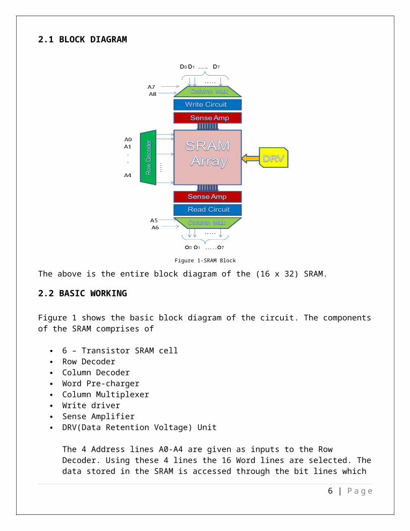
A6 to select the 8 bit word to be written to the SRAM. The DRV unit is initialized on giving the Standby Voltage Supply. On doing so, the SRAM unit alone gets fed with the standby VDD.
3. COMPONENTS
3.1 6T SRAM Cell
The 6T cell stores a bit and its complement inside it. It consists of two access transistors and two in-verters connected back to back to form a latch. The sizing of the inverters and the access transistors could be kept as minimum sizes so that the overall SRAM area is kept minimum. But the scenario of read stability and write stability needs to be taken into consideration.
3.1.1 Schematic
Figure 2- 6T Wire Schematic
Figure 2 shows the schematic of a 6T SRAM cell. M2-M1 and M4-M3 form the cross-coupled inverters that store the actual data. M5 and M6 are the access transistors through which read and write is car-ried out. BL and BL are the bit lines through which data is read and written. WL(Word Line) is the con-trol signal to switch on the access transistors M5 and M6.
3.1.2 Write Operation
For Write Operation, we drive one of the Bit lines high and the other one low and then turn on the word line. The Bit lines overpower the cell with the new values. The new value should be able to over-power the feedback inverters. Assume 1 is stored in the cell(or Q=1). A 0 is written in the cell by set-ting BL to 1 and BL to 0. This causes the inverters to change states if sized properly.
6 | P a g e

During the initiation of a write, the schematic of the SRAM cell be simplified into the model as show in Fig 3. It is reasonable to assume that the gates of transistors M1 and M4 stay at Vdd and GND respec-tively, as long as the switching has not commenced.
Figure 3 - Simplified Operation during Write
Q cannot be pulled high enough to ensure the writing of 1. The sizing constraint, imposed by the read stability, ensures that this voltage is kept below the threshold voltage. Hence, the new value has to be written through transistor M6.
A reliable writing of the cell is ensured if we can pull node Q low enough - this is below the threshold value of the transistor M1. The condition for this can be derived by writing out the dc current equa-tions at the desired threshold point as follows.
Solving for Vq leads to
where Pull-up-ratio (PR) is defined as PR = W4/L4 W6/L6
The value of PR has to be less than 1.8.
3.1.3 Read Operation
7 | P a g e

For Read Operation both the bit lines BL and BL are pre-charged to 1 before the read operation. As-sume that Q is 1, and hence Q has 0. The read cycle is started by asserting the word line, enabling both the access transistors M5 and M6 after the initial word-line delay. During a correct read opera-tion , the values stored in Q and Q are transferred to the bin lines by leaving BL at its pre-charge value and by discharging BL through M1-M5. A careful sizing of the transistors is necessary to avoid acciden-tally writing a 1 into a cell. This type of malfunction is called read upset.
This is illustrated in Fig 3. Consider the BL side of the cell. The bit line capacitance for larger memories
Figure 4- Simplified Operation during Read
is in the pF range. Consequently the value of BL stays at the pre-charged value of Vdd upon enabling of the read operation (WL --> 1). This series combination of the 2 NMOS transistors pulls down the BL towards ground. We would like to have transistors sized as close to minimum as possible, which would result in a very slow discharge of the large bit capacitance. As the difference between the BL and BL builds up, the sense amplifier is activated to accelerate the reading process.
Initially upon the rise of WL, the intermediate node between these 2 NMOS transistors Q, is pulled up towards the precharge value of BL. This voltage rise of Q must stay low enough not to cause a sub-stantial current through the M3-M4, which in the worst case could flip the cells. It is hence necessary to keep the resistance of M5 large than that of M1.
The boundary constraints on the device sizes can be derived by solving the below current equations.
which simplifies to
8 | P a g e

where CR is called the Cell Ratio and is defined as .
To keep the node voltage from rising above transistor threshold (of above 0.7V) the cell ratio must be greater than 1.2V.
According to the design criteria the size of the transistors were chosen as below.
Transistor Sizing Size of the TransistorM2&M4 1.5umM5&M6 3umM1&M3 4.05um
3.2 Layout
Figure 5- Layout of 6T SRAM cell
9 | P a g e

3.3 Schematic
Figure 6 - Schematic of 6T SRAM Cell
4. Word Pre-Charge
The word pre-charger is used to pull the bit and bit bar lines to logic one during read. The word pre charger is created in such a way that it does not fight with NMOS in the back to back connected in-verters so that it does not try to charge the output node connected to the back to back inverters in the case of reading. The input to the word pre charger is given only when a read is to be done. When-ever the read enable goes high, the PMOS is off. So the pseudo NMOS style is avoided to remove the scenario of static power dissipation. The absolute logic “0” cannot be realized in the case of pseudo NMOS style because of the always ON PMOS, due to which the output cannot be pulled to a complete logic “0”.
10 | P a g e

4.1 Layout & Schematic
Figure 7 - Layout & Schematic of Pre-Charge
5. Write Driver
The write driver is designed to write a new bit to a cell or overwrite an already existing value. The write driver has two input pins namely the write data bit and the write enable signal. Once the write enable signal goes high, the write data is pushed onto the appro-priate cell. Note that, both the data ad its complement has to be written into the mem-ory. This is accomplished by using an inverter. Also, the write enable signal drives two transmission gates. The write driver must be capable of writing a clean voltage value on the bit line. There is a big parasitic capacitance seated on the bit line. So the sizing is again based on the method of logical effort.
Figure 8 - Layout of Write Driver
11 | P a g e

Figure 9 - Schematic of Write Driver
6. Entire Memory Design
All the components have been interconnected and the wiring has been done using M1, M2 and M3 metal layer.M1 wires were used for horizontal wiring and M2 wire was used for vertical wiring. M3 wire was used only in the cases where it was unavoidable.
12 | P a g e

Figure 10 - Schematic of 512 SRAM Grid
13 | P a g e

Figure 11 - Layout of 512 SRAM Grid
REFERENCES
[1] Digital Integrated Circuits by Jan M. Rabaey, Anantha Chandrakasan, and Borivoje
Nikolic
[2] SRAM Leakage Suppression by Minimizing Standby Supply Voltage (Dept of EECS,
University of California at Berkeley) Huifang Qin, Yu Cao, Dejan Markovic, Andrei
Vladimirescu, and Jan Rabaey.
14 | P a g e