see datasheet pdf - texas instruments · tps782xx gnd en v in in out v out 1 fm 1 fm on off product...
TRANSCRIPT
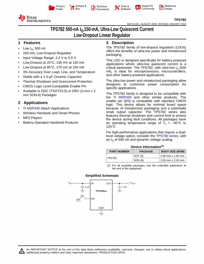
TPS782xx
GND
EN
IN OUTVIN
VOUT
1 Fm1 Fm
On
Off
Product
Folder
Sample &Buy
Technical
Documents
Tools &
Software
Support &Community
ReferenceDesign
TPS782SBVS115D –AUGUST 2008–REVISED JANUARY 2015
TPS782 500-nA IQ,150-mA, Ultra-Low Quiescent CurrentLow-Dropout Linear Regulator
1 Features 3 DescriptionThe TPS782 family of low-dropout regulators (LDOs)
1• Low IQ: 500 nAoffers the benefits of ultra-low power and miniaturized• 150-mA, Low-Dropout Regulator packaging.
• Input Voltage Range: 2.2 V to 5.5 VThis LDO is designed specifically for battery-powered
• Low-Dropout at 25°C, 130 mV at 150 mA applications where ultra-low quiescent current is a• Low-Dropout at 85°C, 175 mV at 150 mA critical parameter. The TPS782, with ultra-low IQ (500
nA), is ideal for microprocessors, microcontrollers,• 3% Accuracy Over Load, Line, and Temperatureand other battery-powered applications.• Stable with a 1.0-μF Ceramic CapacitorThe ultra-low power and miniaturized packaging allow• Thermal Shutdown and Overcurrent Protectiondesigners to customize power consumption for• CMOS Logic Level-Compatible Enable Pin specific applications.
• Available in DDC (TSOT23-5) or DRV (2-mm x 2-The TPS782 family is designed to be compatible withmm SON-6) Packagesthe TI MSP430 and other similar products. Theenable pin (EN) is compatible with standard CMOS2 Applications logic. This device allows for minimal board spacebecause of miniaturized packaging and a potentially• TI MSP430 Attach Applicationssmall output capacitor. The TPS782 series also• Wireless Handsets and Smart Phonesfeatures thermal shutdown and current limit to protect• MP3 Players the device during fault conditions. All packages have
• Battery-Operated Handheld Products an operating temperature range of TJ = –40°C to125°C.
For high-performance applications that require a dual-level voltage option, consider the TPS780 series, withan IQ of 500 nA and dynamic voltage scaling.
Device Information(1)
PART NUMBER PACKAGE BODY SIZE (NOM)SOT (5) 2.90 mm x 1.60 mm
TPS782SON (6) 2.00 mm x 2.00 mm
(1) For all available packages, see the orderable addendum atthe end of the datasheet.
Simplified Schematic
1
An IMPORTANT NOTICE at the end of this data sheet addresses availability, warranty, changes, use in safety-critical applications,intellectual property matters and other important disclaimers. PRODUCTION DATA.
TPS782SBVS115D –AUGUST 2008–REVISED JANUARY 2015 www.ti.com
Table of Contents1 Features .................................................................. 1 8 Application and Implementation ........................ 12
8.1 Application Information............................................ 122 Applications ........................................................... 18.2 Typical Application .................................................. 123 Description ............................................................. 18.3 Do's and Don’ts....................................................... 134 Revision History..................................................... 2
9 Power Supply Recommendations ...................... 135 Pin Configuration and Functions ......................... 310 Layout................................................................... 146 Specifications......................................................... 4
10.1 Layout Guidelines ................................................. 146.1 Absolute Maximum Ratings ...................................... 410.2 Layout Example .................................................... 146.2 ESD Ratings ............................................................ 410.3 Thermal Protection................................................ 146.3 Recommended Operating Conditions....................... 410.4 Power Dissipation ................................................. 146.4 Thermal Information .................................................. 4
11 Device and Documentation Support ................. 156.5 Electrical Characteristics........................................... 511.1 Device Support...................................................... 156.6 Typical Characteristics .............................................. 611.2 Documentation Support ....................................... 157 Detailed Description ............................................ 1011.3 Trademarks ........................................................... 157.1 Overview ................................................................. 1011.4 Electrostatic Discharge Caution............................ 157.2 Functional Block Diagram ....................................... 1011.5 Glossary ................................................................ 157.3 Feature Description................................................. 10
12 Mechanical, Packaging, and Orderable7.4 Device Functional Modes........................................ 11Information ........................................................... 15
4 Revision HistoryNOTE: Page numbers for previous revisions may differ from page numbers in the current version.
Changes from Revision C (January 2014) to Revision D Page
• Added ESD Ratings table, Thermal Information table, Feature Description section, Device Functional Modes,Application and Implementation section, Power Supply Recommendations section, Layout section, Device andDocumentation Support section, and Mechanical, Packaging, and Orderable Information section ..................................... 1
• Changed document format to latest data sheet standards; moved existing sections ............................................................ 1• Changed factory programming feature bullet ........................................................................................................................ 1• Added input voltage range feature bullet ............................................................................................................................... 1• Changed Applications list ...................................................................................................................................................... 1• Changed Description section text (all paragraphs) ................................................................................................................ 1• Added simplified schematic to front page .............................................................................................................................. 1• Deleted footnotes from pin configuration drawings ............................................................................................................... 3• Changed pin descriptions throughout Pin Functions table .................................................................................................... 3• Changed operating junction temperature range maximum value in Absolute Maximum Ratings table................................. 4• Deleted Dissipation Ratings table; see Thermal Information table......................................................................................... 4• Changed symbol and parameter names for clarity in Electrical Characteristics table .......................................................... 5
Changes from Revision B (May 2010) to Revision C Page
• Changed IQ value in Description section from 1 µA to 500 nA .............................................................................................. 1
Changes from Revision A (September 2008) to Revision B Page
• Changed first bullet of Features list........................................................................................................................................ 1• Updated title of data sheet...................................................................................................................................................... 1• Changed ground pin current, IOUT = 0mA typical specification from 1.0 μA to 0.42 μA ......................................................... 5• Added Figure 6 ...................................................................................................................................................................... 6
2 Submit Documentation Feedback Copyright © 2008–2015, Texas Instruments Incorporated
Product Folder Links: TPS782
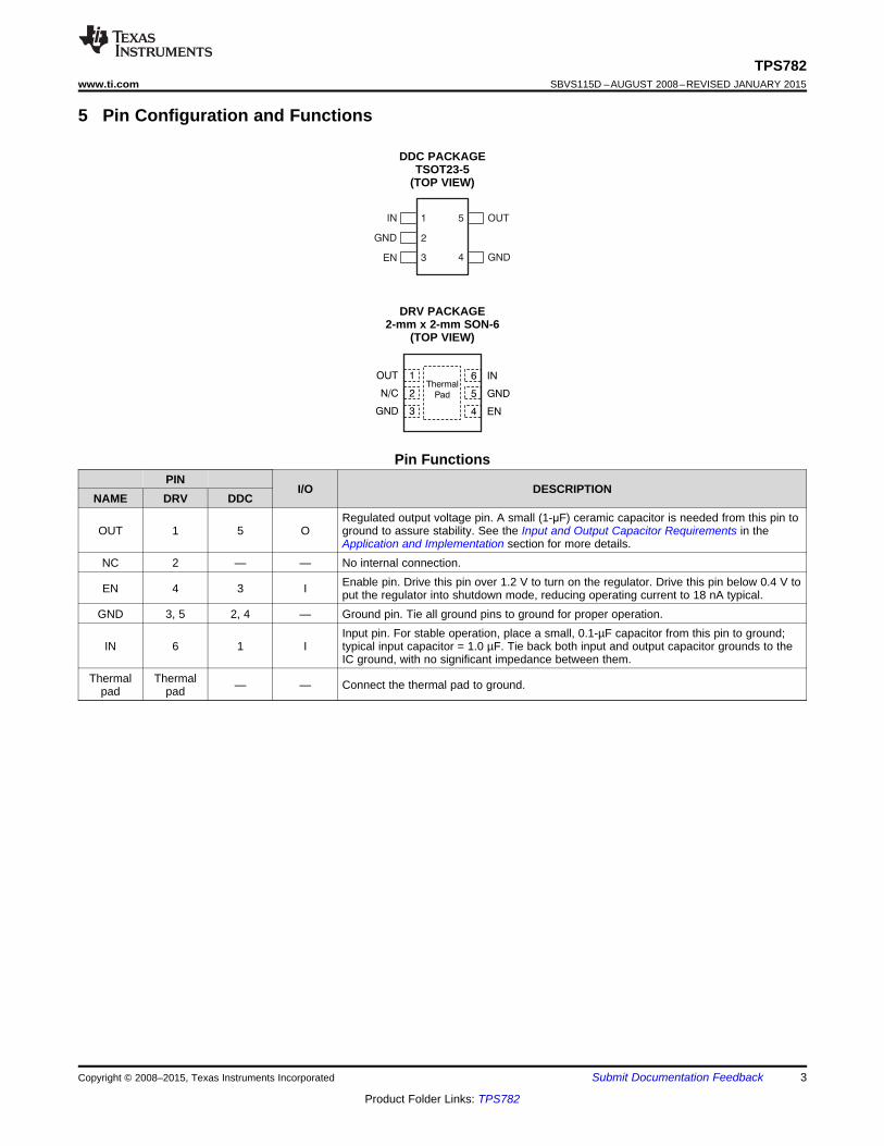
IN
GND
EN
6
5
4
OUT
N/C
GND
1
2
3
Thermal
Pad
OUT
GND
IN
GND
EN
1
2
3
5
4
TPS782www.ti.com SBVS115D –AUGUST 2008–REVISED JANUARY 2015
5 Pin Configuration and Functions
DDC PACKAGETSOT23-5
(TOP VIEW)
DRV PACKAGE2-mm x 2-mm SON-6
(TOP VIEW)
Pin FunctionsPIN
I/O DESCRIPTIONNAME DRV DDC
Regulated output voltage pin. A small (1-μF) ceramic capacitor is needed from this pin toOUT 1 5 O ground to assure stability. See the Input and Output Capacitor Requirements in the
Application and Implementation section for more details.NC 2 — — No internal connection.
Enable pin. Drive this pin over 1.2 V to turn on the regulator. Drive this pin below 0.4 V toEN 4 3 I put the regulator into shutdown mode, reducing operating current to 18 nA typical.GND 3, 5 2, 4 — Ground pin. Tie all ground pins to ground for proper operation.
Input pin. For stable operation, place a small, 0.1-µF capacitor from this pin to ground;IN 6 1 I typical input capacitor = 1.0 µF. Tie back both input and output capacitor grounds to the
IC ground, with no significant impedance between them.Thermal Thermal — — Connect the thermal pad to ground.pad pad
Copyright © 2008–2015, Texas Instruments Incorporated Submit Documentation Feedback 3
Product Folder Links: TPS782
TPS782SBVS115D –AUGUST 2008–REVISED JANUARY 2015 www.ti.com
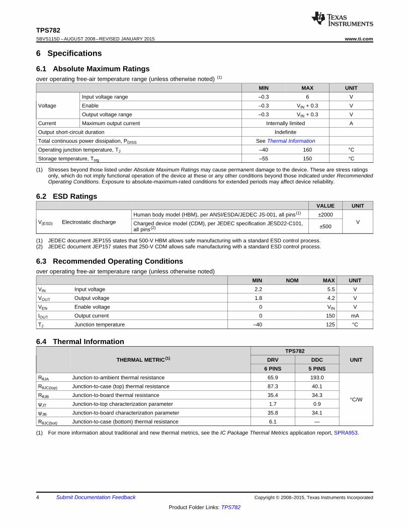
6 Specifications
6.1 Absolute Maximum Ratingsover operating free-air temperature range (unless otherwise noted) (1)
MIN MAX UNITInput voltage range –0.3 6 V
Voltage Enable –0.3 VIN + 0.3 VOutput voltage range –0.3 VIN + 0.3 V
Current Maximum output current Internally limited AOutput short-circuit duration IndefiniteTotal continuous power dissipation, PDISS See Thermal InformationOperating junction temperature, TJ –40 160 °CStorage temperature, Tstg –55 150 °C
(1) Stresses beyond those listed under Absolute Maximum Ratings may cause permanent damage to the device. These are stress ratingsonly, which do not imply functional operation of the device at these or any other conditions beyond those indicated under RecommendedOperating Conditions. Exposure to absolute-maximum-rated conditions for extended periods may affect device reliability.
6.2 ESD RatingsVALUE UNIT
Human body model (HBM), per ANSI/ESDA/JEDEC JS-001, all pins (1) ±2000V(ESD) Electrostatic discharge VCharged device model (CDM), per JEDEC specification JESD22-C101, ±500all pins (2)
(1) JEDEC document JEP155 states that 500-V HBM allows safe manufacturing with a standard ESD control process.(2) JEDEC document JEP157 states that 250-V CDM allows safe manufacturing with a standard ESD control process.
6.3 Recommended Operating Conditionsover operating free-air temperature range (unless otherwise noted)
MIN NOM MAX UNITVIN Input voltage 2.2 5.5 VVOUT Output voltage 1.8 4.2 VVEN Enable voltage 0 VIN VIOUT Output current 0 150 mATJ Junction temperature –40 125 °C
6.4 Thermal InformationTPS782
THERMAL METRIC (1) DRV DDC UNIT6 PINS 5 PINS
RθJA Junction-to-ambient thermal resistance 65.9 193.0RθJC(top) Junction-to-case (top) thermal resistance 87.3 40.1RθJB Junction-to-board thermal resistance 35.4 34.3
°C/WψJT Junction-to-top characterization parameter 1.7 0.9ψJB Junction-to-board characterization parameter 35.8 34.1RθJC(bot) Junction-to-case (bottom) thermal resistance 6.1 —
(1) For more information about traditional and new thermal metrics, see the IC Package Thermal Metrics application report, SPRA953.
4 Submit Documentation Feedback Copyright © 2008–2015, Texas Instruments Incorporated
Product Folder Links: TPS782
TPS782www.ti.com SBVS115D –AUGUST 2008–REVISED JANUARY 2015
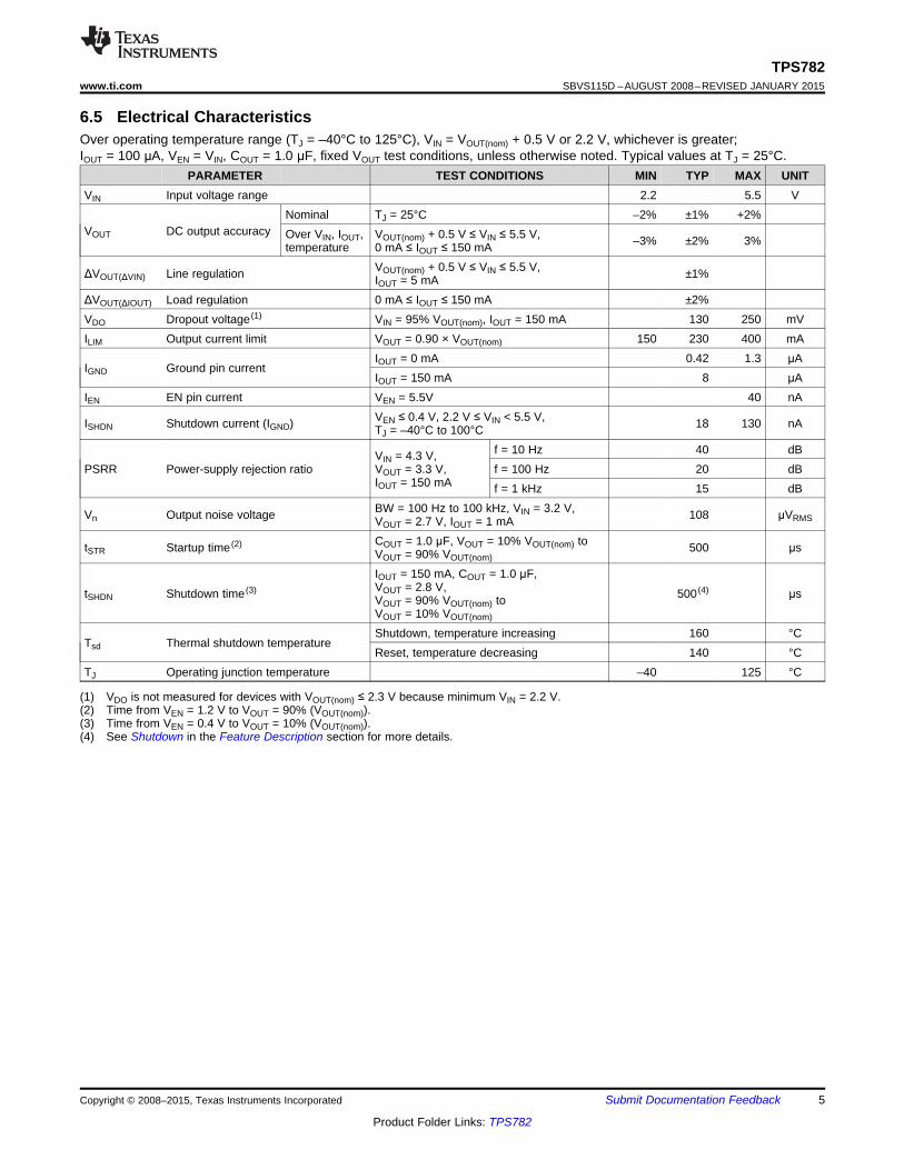
6.5 Electrical CharacteristicsOver operating temperature range (TJ = –40°C to 125°C), VIN = VOUT(nom) + 0.5 V or 2.2 V, whichever is greater;IOUT = 100 μA, VEN = VIN, COUT = 1.0 μF, fixed VOUT test conditions, unless otherwise noted. Typical values at TJ = 25°C.
PARAMETER TEST CONDITIONS MIN TYP MAX UNITVIN Input voltage range 2.2 5.5 V
Nominal TJ = 25°C –2% ±1% +2%VOUT DC output accuracy Over VIN, IOUT, VOUT(nom) + 0.5 V ≤ VIN ≤ 5.5 V, –3% ±2% 3%temperature 0 mA ≤ IOUT ≤ 150 mA
VOUT(nom) + 0.5 V ≤ VIN ≤ 5.5 V,ΔVOUT(ΔVIN) Line regulation ±1%IOUT = 5 mAΔVOUT(ΔIOUT) Load regulation 0 mA ≤ IOUT ≤ 150 mA ±2%VDO Dropout voltage (1) VIN = 95% VOUT(nom), IOUT = 150 mA 130 250 mVILIM Output current limit VOUT = 0.90 × VOUT(nom) 150 230 400 mA
IOUT = 0 mA 0.42 1.3 μAIGND Ground pin current
IOUT = 150 mA 8 μAIEN EN pin current VEN = 5.5V 40 nA
VEN ≤ 0.4 V, 2.2 V ≤ VIN < 5.5 V,ISHDN Shutdown current (IGND) 18 130 nATJ = –40°C to 100°Cf = 10 Hz 40 dBVIN = 4.3 V,
PSRR Power-supply rejection ratio VOUT = 3.3 V, f = 100 Hz 20 dBIOUT = 150 mA f = 1 kHz 15 dBBW = 100 Hz to 100 kHz, VIN = 3.2 V,Vn Output noise voltage 108 μVRMSVOUT = 2.7 V, IOUT = 1 mACOUT = 1.0 μF, VOUT = 10% VOUT(nom) totSTR Startup time (2) 500 μsVOUT = 90% VOUT(nom)
IOUT = 150 mA, COUT = 1.0 μF,VOUT = 2.8 V,tSHDN Shutdown time (3) 500 (4) μsVOUT = 90% VOUT(nom) toVOUT = 10% VOUT(nom)
Shutdown, temperature increasing 160 °CTsd Thermal shutdown temperature
Reset, temperature decreasing 140 °CTJ Operating junction temperature –40 125 °C
(1) VDO is not measured for devices with VOUT(nom) ≤ 2.3 V because minimum VIN = 2.2 V.(2) Time from VEN = 1.2 V to VOUT = 90% (VOUT(nom)).(3) Time from VEN = 0.4 V to VOUT = 10% (VOUT(nom)).(4) See Shutdown in the Feature Description section for more details.
Copyright © 2008–2015, Texas Instruments Incorporated Submit Documentation Feedback 5
Product Folder Links: TPS782

900
800
700
600
500
400
300
200
100
0
I(n
A)
GN
D
V (V)IN
3.8 4.0 4.2 4.4 4.6 4.8 5.0 5.2 5.4 5.6
T = +25 C°J
T = +125 C°J
T = +85 C°J
T = 40 C- °J
-40 -25 -10 1251109580655035205
TJ ( C)°
V(V
V-
DO
INO
UT)
(mV
)
250
200
150
100
50
0
150mA
100mA
50mA
10mA
0 25 50 75 100 125 150
I (mA)OUT
V(%
)O
UT
3
2
1
0
-1
-2
-3
TJ = +85°C
T = 40- °J C
TJ = +25°C
0 25 50 75 100 125 150
I (mA)OUT
V(V
V-
DO
INO
UT)
(mV
)
250
200
150
100
50
0
TJ = +125°C
TJ = +85°C
T = 40- °J CTJ = +25°C
3.8 4.0 4.2 4.4 4.6 4.8 5.0 5.2 5.4 5.6
V (V)IN
V(%
)O
UT
1.0
0.8
0.6
0.4
0.2
0
-0.2
-0.4
-0.6
-0.8
-1.0
T = +85°J C
T = 40- °J C
T = +25°J C
3.8 4.0 4.2 4.4 4.6 4.8 5.0 5.2 5.4 5.6
V (V)IN
V(%
)O
UT
3
2
1
0
-1
-2
-3
TJ = +85°C
T 40- °J = C
TJ = +25°C
TPS782SBVS115D –AUGUST 2008–REVISED JANUARY 2015 www.ti.com
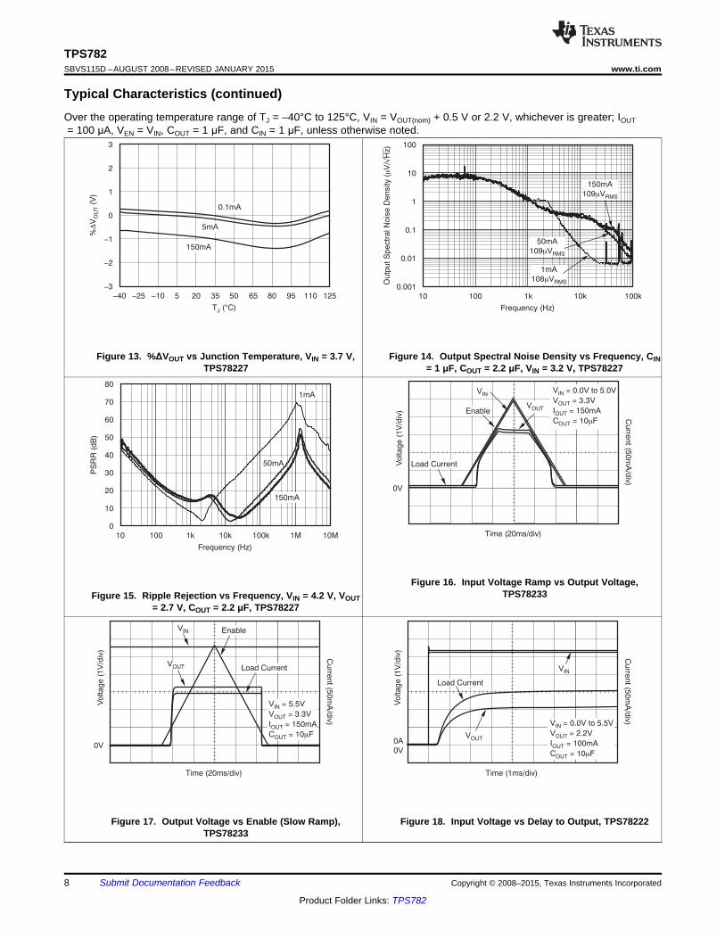
6.6 Typical CharacteristicsOver the operating temperature range of TJ = –40°C to 125°C, VIN = VOUT(nom) + 0.5 V or 2.2 V, whichever is greater; IOUT= 100 μA, VEN = VIN, COUT = 1 μF, and CIN = 1 μF, unless otherwise noted.
Figure 1. Line Regulation, IOUT = 5 mA, TPS78227 Figure 2. Line Regulation, IOUT = 150 mA, TPS78227
Figure 3. Load Regulation, VIN = 3.8 V, TPS78227 Figure 4. Dropout Voltage vs Output Current, VIN = 0.95 ×VOUT(nom), TPS78227
Figure 5. Dropout Voltage vs Junction Temperature, VIN = Figure 6. Ground Pin Current vs Input Voltage, IOUT = 0 mA,0.95 × VOUT(nom), TPS78227 TPS78233
6 Submit Documentation Feedback Copyright © 2008–2015, Texas Instruments Incorporated
Product Folder Links: TPS782

-40 -25 -10 1251109580655035205
T ( C)°J
V(V
)E
N
1.2
1.1
1.0
0.9
0.8
0.7
0.6
0.5
0.4
V OnEN
V OffEN
-40 -25 -10 1251109580655035205
TJ ( C)°
%D
VO
UT
(V)
1
0
-1
-2
150mA
0.1mA
5mA
3.8 4.0 4.2 4.4 4.6 4.8 5.0 5.2 5.4 5.6
V (V)IN
Cu
rre
nt
Lim
it (
mA
)
300
290
280
270
260
250
240
230
220
210
200
TJ = +125°C
TJ = +85°C
T = 40- °J C
TJ = +25°C
3.8 4.0 4.2 4.4 4.6 4.8 5.0 5.2 5.4 5.6
V (V)IN
I(n
A)
EN
2.0
1.8
1.6
1.4
1.2
1.0
0.8
0.6
0.4
0.2
0
TJ = +85°C
T = 40- °J C
TJ = +25°C
3.8 4.0 4.2 4.4 4.6 4.8 5.0 5.2 5.4 5.6
V (V)IN
I(
A)
mG
ND
6
5
4
3
2
1
0
T = +125 C°JT = +85 C°J
T 40- °J = CT = +25 C°J
3.8 4.0 4.2 4.4 4.6 4.8 5.0 5.2 5.4 5.6
V (V)IN
V(%
)O
UT
3
2
1
0
-1
-2
-3
TJ = +85°C
T 40- °J = C
TJ = +25°C
TPS782www.ti.com SBVS115D –AUGUST 2008–REVISED JANUARY 2015
Typical Characteristics (continued)Over the operating temperature range of TJ = –40°C to 125°C, VIN = VOUT(nom) + 0.5 V or 2.2 V, whichever is greater; IOUT= 100 μA, VEN = VIN, COUT = 1 μF, and CIN = 1 μF, unless otherwise noted.
Figure 7. Ground Pin Current vs Input Voltage, IOUT = 50 Figure 8. Ground Pin Current vs Input Voltage, IOUT = 150mA, TPS78227 mA, TPS78227
Figure 9. Current Limit vs Input Voltage, VOUT = 95% Figure 10. Enable Pin Current vs Input Voltage, IOUT = 100VOUT(nom), TPS78227 μA, TPS78227
Figure 11. Enable Pin Hysteresis vs Junction Temperature, Figure 12. %ΔVOUT vs Junction Temperature, VIN = 3.3 V,IOUT = 1 mA, TPS78227 TPS78227
Copyright © 2008–2015, Texas Instruments Incorporated Submit Documentation Feedback 7
Product Folder Links: TPS782
Vo
lta
ge
(1
V/d
iv)
Time (20ms/div)
V = 5.5VIN
V = 3.3VOUT
I = 150mAOUT
C = 10 FmOUT
VIN
VOUT Load Current
Enable
0V
Cu
rren
t (50
mA
/div
)V
olta
ge
(1
V/d
iv)
Time (1ms/div)
Load Current
V = 0.0V to 5.5VIN
V = 2.2VOUT
I = 100mAOUT
C = 10 FmOUT
VIN
VOUT0A
0V
Cu
rren
t (50
mA
/div
)
10 10M100 1k 10k 100k 1M
Frequency (Hz)
PS
RR
(d
B)
80
70
60
50
40
30
20
10
0
150mA
50mA
1mAV
olta
ge
(1
V/d
iv)
Time (20ms/div)
Load Current
EnableVOUT
VINV = 0.0V toIN 5.0V
V = 3.3VOUT
I = 150mAOUT
C = 10 FmOUT
0V
Cu
rren
t (50
mA
/div
)
-40 -25 -10 1251109580655035205
TJ ( C)°
%V
(V)
DO
UT
3
2
1
0
-1
-2
-3
150mA
0.1mA
5mA
10 100 1k 10k 100k
Frequency (Hz)
Ou
tpu
t S
pe
ctr
al N
ois
e D
en
sity (
V/
)m
ÖH
z
100
10
1
0.1
0.01
0.001
150mA
109 Vm RMS
50mA
109 Vm RMS
1mA
108 Vm RMS
TPS782SBVS115D –AUGUST 2008–REVISED JANUARY 2015 www.ti.com
Typical Characteristics (continued)Over the operating temperature range of TJ = –40°C to 125°C, VIN = VOUT(nom) + 0.5 V or 2.2 V, whichever is greater; IOUT= 100 μA, VEN = VIN, COUT = 1 μF, and CIN = 1 μF, unless otherwise noted.
Figure 13. %ΔVOUT vs Junction Temperature, VIN = 3.7 V, Figure 14. Output Spectral Noise Density vs Frequency, CINTPS78227 = 1 μF, COUT = 2.2 μF, VIN = 3.2 V, TPS78227
Figure 16. Input Voltage Ramp vs Output Voltage,TPS78233Figure 15. Ripple Rejection vs Frequency, VIN = 4.2 V, VOUT
= 2.7 V, COUT = 2.2 μF, TPS78227
Figure 17. Output Voltage vs Enable (Slow Ramp), Figure 18. Input Voltage vs Delay to Output, TPS78222TPS78233
8 Submit Documentation Feedback Copyright © 2008–2015, Texas Instruments Incorporated
Product Folder Links: TPS782

Vo
lta
ge
(1
V/d
iv)
Time (1ms/div)
Load
Current
V = 5.5VIN
V = 3.3VOUT
I = 150mAOUT
C = 10 FmOUT
VINVOUT
Enable
0V
Cu
rren
t (50
mA
/div
)
Vo
lta
ge
(10
0m
V/d
iv)
Time (5ms/div)
Load
Current
V = 5.5VIN
V = 3.3VOUT
I = 0mA to 10mAOUT
C = 10 FmOUT
VOUT
EnableVIN
Cu
rren
t
(10
mA
/div
)
0A
Vo
lta
ge
(1
V/d
iv)
Time (1ms/div)
Load Current
V = 5.50VIN
V = 3.3VOUT
I = 150mAOUT
COUT = 10mF
VINVOUT
Enable
0V
Cu
rren
t (50
mA
/div
)
TPS782www.ti.com SBVS115D –AUGUST 2008–REVISED JANUARY 2015
Typical Characteristics (continued)Over the operating temperature range of TJ = –40°C to 125°C, VIN = VOUT(nom) + 0.5 V or 2.2 V, whichever is greater; IOUT= 100 μA, VEN = VIN, COUT = 1 μF, and CIN = 1 μF, unless otherwise noted.
Figure 19. Load Transient Response, TPS78233 Figure 20. Enable Pin vs Output Voltage Response andOutput Current, TPS78233
Figure 21. Enable Pin vs Output Voltage Delay, TPS78233
Copyright © 2008–2015, Texas Instruments Incorporated Submit Documentation Feedback 9
Product Folder Links: TPS782
ThermalShutdown
10kW
CurrentLimit
Bandgap
IN
EN
OUT
EPROMM
ux
Logic
ActivePull-
Down
GND
TPS782SBVS115D –AUGUST 2008–REVISED JANUARY 2015 www.ti.com
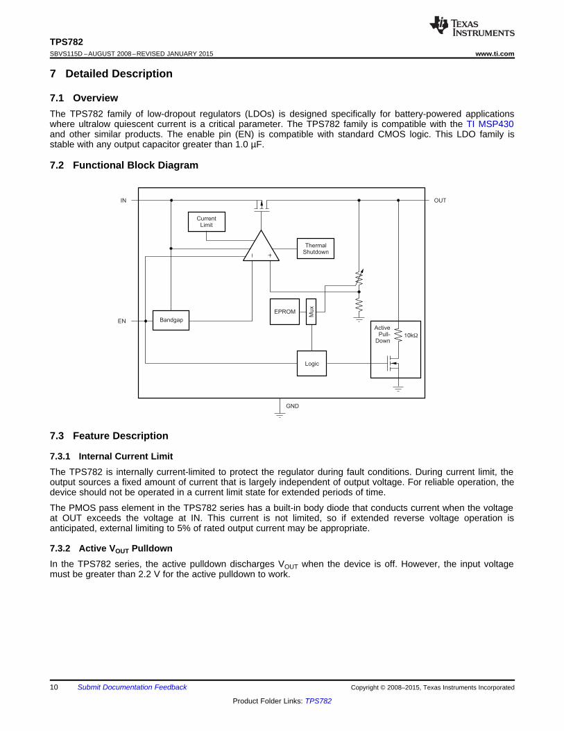
7 Detailed Description
7.1 OverviewThe TPS782 family of low-dropout regulators (LDOs) is designed specifically for battery-powered applicationswhere ultralow quiescent current is a critical parameter. The TPS782 family is compatible with the TI MSP430and other similar products. The enable pin (EN) is compatible with standard CMOS logic. This LDO family isstable with any output capacitor greater than 1.0 µF.
7.2 Functional Block Diagram
7.3 Feature Description
7.3.1 Internal Current LimitThe TPS782 is internally current-limited to protect the regulator during fault conditions. During current limit, theoutput sources a fixed amount of current that is largely independent of output voltage. For reliable operation, thedevice should not be operated in a current limit state for extended periods of time.
The PMOS pass element in the TPS782 series has a built-in body diode that conducts current when the voltageat OUT exceeds the voltage at IN. This current is not limited, so if extended reverse voltage operation isanticipated, external limiting to 5% of rated output current may be appropriate.
7.3.2 Active VOUT PulldownIn the TPS782 series, the active pulldown discharges VOUT when the device is off. However, the input voltagemust be greater than 2.2 V for the active pulldown to work.
10 Submit Documentation Feedback Copyright © 2008–2015, Texas Instruments Incorporated
Product Folder Links: TPS782
TPS78227
GND
EN
IN OUTVIN
VOUT
1 Fm1 Fm
4.2V to 5.5V 2.7V
t = 310k RW
L´
10kW + RL
COUT
´
TPS782www.ti.com SBVS115D –AUGUST 2008–REVISED JANUARY 2015
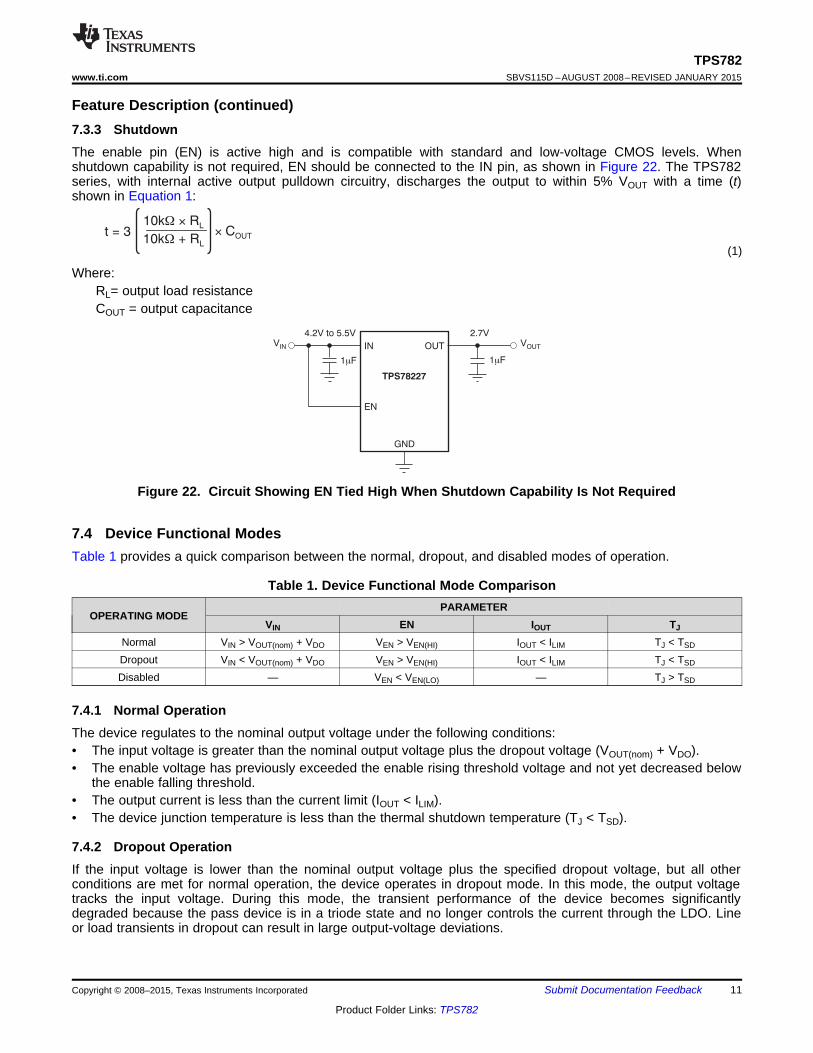
Feature Description (continued)7.3.3 ShutdownThe enable pin (EN) is active high and is compatible with standard and low-voltage CMOS levels. Whenshutdown capability is not required, EN should be connected to the IN pin, as shown in Figure 22. The TPS782series, with internal active output pulldown circuitry, discharges the output to within 5% VOUT with a time (t)shown in Equation 1:
(1)
Where:RL= output load resistanceCOUT = output capacitance
Figure 22. Circuit Showing EN Tied High When Shutdown Capability Is Not Required
7.4 Device Functional ModesTable 1 provides a quick comparison between the normal, dropout, and disabled modes of operation.
Table 1. Device Functional Mode ComparisonPARAMETER
OPERATING MODEVIN EN IOUT TJ
Normal VIN > VOUT(nom) + VDO VEN > VEN(HI) IOUT < ILIM TJ < TSD
Dropout VIN < VOUT(nom) + VDO VEN > VEN(HI) IOUT < ILIM TJ < TSD
Disabled — VEN < VEN(LO) — TJ > TSD
7.4.1 Normal OperationThe device regulates to the nominal output voltage under the following conditions:• The input voltage is greater than the nominal output voltage plus the dropout voltage (VOUT(nom) + VDO).• The enable voltage has previously exceeded the enable rising threshold voltage and not yet decreased below
the enable falling threshold.• The output current is less than the current limit (IOUT < ILIM).• The device junction temperature is less than the thermal shutdown temperature (TJ < TSD).
7.4.2 Dropout OperationIf the input voltage is lower than the nominal output voltage plus the specified dropout voltage, but all otherconditions are met for normal operation, the device operates in dropout mode. In this mode, the output voltagetracks the input voltage. During this mode, the transient performance of the device becomes significantlydegraded because the pass device is in a triode state and no longer controls the current through the LDO. Lineor load transients in dropout can result in large output-voltage deviations.
Copyright © 2008–2015, Texas Instruments Incorporated Submit Documentation Feedback 11
Product Folder Links: TPS782
TPS782xx
GND
EN
IN OUTVIN
VOUT
1 Fm1 Fm
On
Off
TPS782SBVS115D –AUGUST 2008–REVISED JANUARY 2015 www.ti.com
7.4.3 DisabledThe device is disabled under the following conditions:• The enable voltage is less than the enable falling threshold voltage or has not yet exceeded the enable rising
threshold.• The device junction temperature is greater than the thermal shutdown temperature (TJ > TSD).
8 Application and Implementation
NOTEInformation in the following applications sections is not part of the TI componentspecification, and TI does not warrant its accuracy or completeness. TI’s customers areresponsible for determining suitability of components for their purposes. Customers shouldvalidate and test their design implementation to confirm system functionality.
8.1 Application InformationThe TPS782 family of LDOs is factory-programmable to have a fixed output. Note that during startup or steady-state conditions, it is important that the EN pin voltage never exceed VIN + 0.3V.
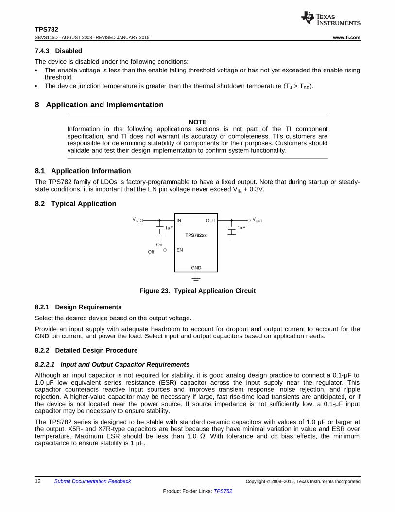
8.2 Typical Application
Figure 23. Typical Application Circuit
8.2.1 Design RequirementsSelect the desired device based on the output voltage.
Provide an input supply with adequate headroom to account for dropout and output current to account for theGND pin current, and power the load. Select input and output capacitors based on application needs.
8.2.2 Detailed Design Procedure
8.2.2.1 Input and Output Capacitor RequirementsAlthough an input capacitor is not required for stability, it is good analog design practice to connect a 0.1-μF to1.0-μF low equivalent series resistance (ESR) capacitor across the input supply near the regulator. Thiscapacitor counteracts reactive input sources and improves transient response, noise rejection, and ripplerejection. A higher-value capacitor may be necessary if large, fast rise-time load transients are anticipated, or ifthe device is not located near the power source. If source impedance is not sufficiently low, a 0.1-μF inputcapacitor may be necessary to ensure stability.
The TPS782 series is designed to be stable with standard ceramic capacitors with values of 1.0 μF or larger atthe output. X5R- and X7R-type capacitors are best because they have minimal variation in value and ESR overtemperature. Maximum ESR should be less than 1.0 Ω. With tolerance and dc bias effects, the minimumcapacitance to ensure stability is 1 μF.
12 Submit Documentation Feedback Copyright © 2008–2015, Texas Instruments Incorporated
Product Folder Links: TPS782

10 100 1k 10k 100k
Frequency (Hz)
Ou
tpu
t S
pe
ctr
al N
ois
e D
ensity (
V/
)m
ÖH
z
100
10
1
0.1
0.01
0.001
150mA
109 Vm RMS
50mA
109 Vm RMS
1mA
108 Vm RMS
10 10M100 1k 10k 100k 1M
Frequency (Hz)
PS
RR
(dB
)
80
70
60
50
40
30
20
10
0
150mA
50mA
1mA
TPS782www.ti.com SBVS115D –AUGUST 2008–REVISED JANUARY 2015
Typical Application (continued)8.2.2.2 Dropout VoltageThe TPS782 uses a PMOS pass transistor to achieve low dropout. When (VIN – VOUT) is less than the dropoutvoltage (VDO), the PMOS pass device is the linear region of operation and the input-to-output resistance is theRDS(ON) of the PMOS pass element. VDO approximately scales with output current because the PMOS devicebehaves like a resistor in dropout. As with any linear regulator, PSRR and transient response are degraded as(VIN – VOUT) approaches dropout. This effect is shown in the Typical Characteristics section. Refer to applicationreport SLVA207, Understanding LDO Dropout, available for download from www.ti.com.
8.2.2.3 Transient ResponseAs with any regulator, increasing the size of the output capacitor reduces over/undershoot magnitude butincreases duration of the transient response. For more information, see Figure 19.
8.2.2.4 Minimum LoadThe TPS782 series is stable with no output load. Traditional PMOS LDO regulators suffer from lower loop gain atvery light output loads. The TPS782 employs an innovative, low-current circuit under very light or no-loadconditions, resulting in improved output voltage regulation performance down to zero output current. SeeFigure 19 for the load transient response.
8.2.3 Application Curves
Figure 24. Output Spectral Noise Density vs Frequency, Figure 25. Ripple Rejection vs Frequency, VIN = 4.2 V,CIN = 1 μF, COUT = 2.2 μF, VIN = 3.2 V, TPS78227 VOUT = 2.7 V, COUT = 2.2 μF, TPS78227
8.3 Do's and Don’tsDo place at least one 1-µF ceramic capacitor as close as possible to the OUT pin of the regulator.
Do not place the output capacitor more than 10 mm away from the regulator.
Do connect a 0.1-μF to 1.0-μF low equivalent series resistance (ESR) capacitor across the IN pin and GND ofthe regulator.
Do not exceed the absolute maximum ratings.
9 Power Supply RecommendationsFor best performance, connect a low-output impedance power supply directly to the IN pin of the TPS782 series.Inductive impedances between the input supply and the IN pin create significant voltage excursions at the IN pinduring startup or load transient events. If inductive impedances are unavoidable, use an input capacitor.
Copyright © 2008–2015, Texas Instruments Incorporated Submit Documentation Feedback 13
Product Folder Links: TPS782

P = (V V ) I- ´D IN OUT OUT
Represents via used forapplication-specific connections
VOUTVIN
CIN COUT
GND PLANE
1
2
3 4
5
TPS782SBVS115D –AUGUST 2008–REVISED JANUARY 2015 www.ti.com
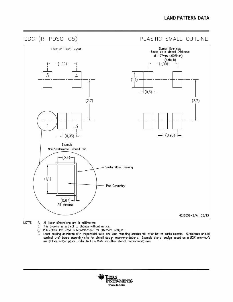
10 Layout
10.1 Layout GuidelinesTo improve ac performance (such as PSRR, output noise, and transient response), it is recommended that theprinted circuit board (PCB) be designed with separate ground planes for VIN and VOUT, with each ground planeconnected only at the GND pin of the device. In addition, the ground connection for the output capacitor shouldconnect directly to the GND pin of the device. High ESR capacitors may degrade PSRR.
10.2 Layout Example
Figure 26. Layout Example for DDC Package
10.3 Thermal ProtectionThermal protection disables the device output when the junction temperature rises to approximately 160°C,allowing the device to cool. Once the junction temperature cools to approximately 140°C, the output circuitry isenabled. Depending on power dissipation, thermal resistance, and ambient temperature, the thermal protectioncircuit may cycle on and off again. This cycling limits the dissipation of the regulator, protecting it from damageas a result of overheating.
Any tendency to activate the thermal protection circuit indicates excessive power dissipation or an inadequateheatsink. For reliable operation, junction temperature should be limited to 125°C maximum. To estimate themargin of safety in a complete design (including heatsink), increase the ambient temperature until the thermalprotection is triggered; use worst-case loads and signal conditions. For good reliability, thermal protection shouldtrigger at least 35°C above the maximum expected ambient condition of your particular application. Thisconfiguration produces a worst-case junction temperature of 125°C at the highest expected ambient temperatureand worst-case load.
The internal protection circuitry of the TPS782 series has been designed to protect against overload conditions.However, it is not intended to replace proper heatsinking. Continuously running the TPS782 series into thermalshutdown degrades device reliability.
10.4 Power DissipationThe ability to remove heat from the die is different for each package type, presenting different considerations inthe PCB layout. The PCB area around the device that is free of other components moves the heat from thedevice to the ambient air. Performance data for JEDEC low- and high-K boards are given in the ThermalInformation table. Using heavier copper increases the effectiveness in removing heat from the device. Theaddition of plated through-holes to heat-dissipating layers also improves the heatsink effectiveness. Powerdissipation depends on input voltage and load conditions. Power dissipation (PD) is equal to the product of theoutput current times the voltage drop across the output pass element (VIN to VOUT), as shown in Equation 2:
(2)
14 Submit Documentation Feedback Copyright © 2008–2015, Texas Instruments Incorporated
Product Folder Links: TPS782

TPS782www.ti.com SBVS115D –AUGUST 2008–REVISED JANUARY 2015
11 Device and Documentation Support
11.1 Device Support
11.1.1 Development Support
11.1.1.1 Evaluation ModulesAn evaluation module (EVM) is available to assist in the initial circuit performance evaluation using the TPS782.The TPS782xxEVM evaluation modules (and related user guide) can be requested at the Texas Instrumentswebsite through the product folders or purchased directly from the TI eStore.
11.1.1.2 Spice ModelsComputer simulation of circuit performance using SPICE is often useful when analyzing the performance ofanalog circuits and systems. A SPICE model for the TPS782 family is available through the product folders underSimulation Models.
11.1.2 Device Nomenclature
Table 2. Device Nomenclature (1)
PRODUCT VOUT
TPS782xxyyyz XX is the nominal output voltageYYY is the package designator.Z is the tape and reel quantity (R = 3000, T = 250).
(1) For the most current package and ordering information see the Package Option Addendum at the end of this document, or see the TIweb site at www.ti.com.
11.2 Documentation Support
11.2.1 Related DocumentationFor related documentation see the following:• Application report. Understanding LDO Dropout, SLVA207• Product information. Low-power MCUs, MSP430• Reference design.Water Meter Implementation with FRAM Microcontroller, TIDU517
11.3 TrademarksAll trademarks are the property of their respective owners.
11.4 Electrostatic Discharge CautionThese devices have limited built-in ESD protection. The leads should be shorted together or the device placed in conductive foamduring storage or handling to prevent electrostatic damage to the MOS gates.
11.5 GlossarySLYZ022 — TI Glossary.
This glossary lists and explains terms, acronyms, and definitions.
12 Mechanical, Packaging, and Orderable InformationThe following pages include mechanical, packaging, and orderable information. This information is the mostcurrent data available for the designated devices. This data is subject to change without notice and revision ofthis document. For browser-based versions of this data sheet, refer to the left-hand navigation.
Copyright © 2008–2015, Texas Instruments Incorporated Submit Documentation Feedback 15
Product Folder Links: TPS782

PACKAGE OPTION ADDENDUM
www.ti.com 7-Sep-2017
Addendum-Page 1
PACKAGING INFORMATION
Orderable Device Status(1)
Package Type PackageDrawing
Pins PackageQty
Eco Plan(2)
Lead/Ball Finish(6)
MSL Peak Temp(3)
Op Temp (°C) Device Marking(4/5)
Samples
TPS78218DDCR ACTIVE SOT-23-THIN DDC 5 3000 Green (RoHS& no Sb/Br)
CU NIPDAU Level-2-260C-1 YEAR -40 to 125 SJY
TPS78218DDCT ACTIVE SOT-23-THIN DDC 5 250 Green (RoHS& no Sb/Br)
CU NIPDAU Level-2-260C-1 YEAR -40 to 125 SJY
TPS78218DRVR ACTIVE WSON DRV 6 3000 Green (RoHS& no Sb/Br)
CU NIPDAU Level-1-260C-UNLIM -40 to 125 SAF
TPS78218DRVT ACTIVE WSON DRV 6 250 Green (RoHS& no Sb/Br)
CU NIPDAU Level-1-260C-UNLIM -40 to 125 SAF
TPS78222DRVR ACTIVE WSON DRV 6 3000 Green (RoHS& no Sb/Br)
CU NIPDAU Level-1-260C-UNLIM -40 to 125 RAR
TPS78222DRVT ACTIVE WSON DRV 6 250 Green (RoHS& no Sb/Br)
CU NIPDAU Level-1-260C-UNLIM -40 to 125 RAR
TPS78223DDCR ACTIVE SOT-23-THIN DDC 5 3000 Green (RoHS& no Sb/Br)
CU NIPDAU Level-2-260C-1 YEAR -40 to 125 NXM
TPS78223DDCT ACTIVE SOT-23-THIN DDC 5 250 Green (RoHS& no Sb/Br)
CU NIPDAU Level-2-260C-1 YEAR -40 to 125 NXM
TPS78225DDCR ACTIVE SOT-23-THIN DDC 5 3000 Green (RoHS& no Sb/Br)
CU NIPDAU Level-2-260C-1 YEAR -40 to 125 CVD
TPS78225DDCRG4 ACTIVE SOT-23-THIN DDC 5 3000 Green (RoHS& no Sb/Br)
CU NIPDAU Level-2-260C-1 YEAR -40 to 125 CVD
TPS78225DDCT ACTIVE SOT-23-THIN DDC 5 250 Green (RoHS& no Sb/Br)
CU NIPDAU Level-2-260C-1 YEAR -40 to 125 CVD
TPS78225DDCTG4 ACTIVE SOT-23-THIN DDC 5 250 Green (RoHS& no Sb/Br)
CU NIPDAU Level-2-260C-1 YEAR -40 to 125 CVD
TPS78225DRVR ACTIVE WSON DRV 6 3000 Green (RoHS& no Sb/Br)
CU NIPDAU Level-1-260C-UNLIM -40 to 125 CVD
TPS78225DRVT ACTIVE WSON DRV 6 250 Green (RoHS& no Sb/Br)
CU NIPDAU Level-1-260C-UNLIM -40 to 125 CVD
TPS78225DRVTG4 ACTIVE WSON DRV 6 250 Green (RoHS& no Sb/Br)
CU NIPDAU Level-1-260C-UNLIM -40 to 125 CVD
TPS78227DDCR ACTIVE SOT-23-THIN DDC 5 3000 Green (RoHS& no Sb/Br)
CU NIPDAU Level-2-260C-1 YEAR -40 to 125 CVE
TPS78227DDCRG4 ACTIVE SOT-23-THIN DDC 5 3000 Green (RoHS& no Sb/Br)
CU NIPDAU Level-2-260C-1 YEAR -40 to 125 CVE

PACKAGE OPTION ADDENDUM
www.ti.com 7-Sep-2017
Addendum-Page 2
Orderable Device Status(1)
Package Type PackageDrawing
Pins PackageQty
Eco Plan(2)
Lead/Ball Finish(6)
MSL Peak Temp(3)
Op Temp (°C) Device Marking(4/5)
Samples
TPS78227DDCT ACTIVE SOT-23-THIN DDC 5 250 Green (RoHS& no Sb/Br)
CU NIPDAU Level-2-260C-1 YEAR -40 to 125 CVE
TPS78227DDCTG4 ACTIVE SOT-23-THIN DDC 5 250 Green (RoHS& no Sb/Br)
CU NIPDAU Level-2-260C-1 YEAR -40 to 125 CVE
TPS78227DRVR ACTIVE WSON DRV 6 3000 Green (RoHS& no Sb/Br)
CU NIPDAU Level-1-260C-UNLIM -40 to 125 CVE
TPS78227DRVT ACTIVE WSON DRV 6 250 Green (RoHS& no Sb/Br)
CU NIPDAU Level-1-260C-UNLIM -40 to 125 CVE
TPS78227DRVTG4 ACTIVE WSON DRV 6 250 Green (RoHS& no Sb/Br)
CU NIPDAU Level-1-260C-UNLIM -40 to 125 CVE
TPS78228DDCR ACTIVE SOT-23-THIN DDC 5 3000 Green (RoHS& no Sb/Br)
CU NIPDAU Level-2-260C-1 YEAR -40 to 125 CVF
TPS78228DDCRG4 ACTIVE SOT-23-THIN DDC 5 3000 Green (RoHS& no Sb/Br)
CU NIPDAU Level-2-260C-1 YEAR -40 to 125 CVF
TPS78228DDCT ACTIVE SOT-23-THIN DDC 5 250 Green (RoHS& no Sb/Br)
CU NIPDAU Level-2-260C-1 YEAR -40 to 125 CVF
TPS78228DDCTG4 ACTIVE SOT-23-THIN DDC 5 250 Green (RoHS& no Sb/Br)
CU NIPDAU Level-2-260C-1 YEAR -40 to 125 CVF
TPS78228DRVR ACTIVE WSON DRV 6 3000 Green (RoHS& no Sb/Br)
CU NIPDAU |CU NIPDAUAG
Level-1-260C-UNLIM -40 to 125 CVF
TPS78228DRVRG4 ACTIVE WSON DRV 6 3000 Green (RoHS& no Sb/Br)
CU NIPDAUAG Level-1-260C-UNLIM -40 to 125 CVF
TPS78228DRVT ACTIVE WSON DRV 6 250 Green (RoHS& no Sb/Br)
CU NIPDAU |CU NIPDAUAG
Level-1-260C-UNLIM -40 to 125 CVF
TPS78230DDCR ACTIVE SOT-23-THIN DDC 5 3000 Green (RoHS& no Sb/Br)
CU NIPDAU Level-2-260C-1 YEAR -40 to 125 OCK
TPS78230DDCT ACTIVE SOT-23-THIN DDC 5 250 Green (RoHS& no Sb/Br)
CU NIPDAU Level-2-260C-1 YEAR -40 to 125 OCK
TPS78230DRVR ACTIVE WSON DRV 6 3000 Green (RoHS& no Sb/Br)
CU NIPDAU Level-1-260C-UNLIM -40 to 125 ODE
TPS78230DRVT ACTIVE WSON DRV 6 250 Green (RoHS& no Sb/Br)
CU NIPDAU Level-1-260C-UNLIM -40 to 125 ODE
TPS78233DDCR ACTIVE SOT-23-THIN DDC 5 3000 Green (RoHS& no Sb/Br)
CU NIPDAU Level-2-260C-1 YEAR -40 to 125 OAH
TPS78233DDCT ACTIVE SOT-23-THIN DDC 5 250 Green (RoHS& no Sb/Br)
CU NIPDAU Level-2-260C-1 YEAR -40 to 125 OAH
PACKAGE OPTION ADDENDUM
www.ti.com 7-Sep-2017
Addendum-Page 3
Orderable Device Status(1)
Package Type PackageDrawing
Pins PackageQty
Eco Plan(2)
Lead/Ball Finish(6)
MSL Peak Temp(3)
Op Temp (°C) Device Marking(4/5)
Samples
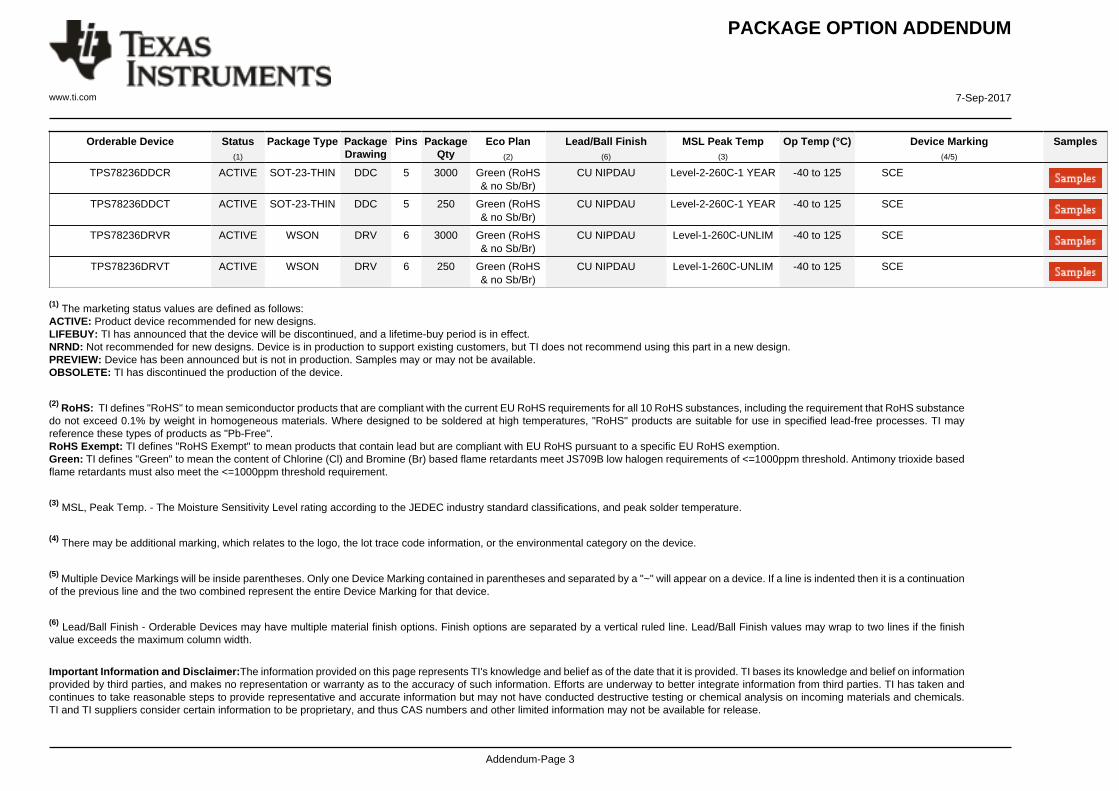
TPS78236DDCR ACTIVE SOT-23-THIN DDC 5 3000 Green (RoHS& no Sb/Br)
CU NIPDAU Level-2-260C-1 YEAR -40 to 125 SCE
TPS78236DDCT ACTIVE SOT-23-THIN DDC 5 250 Green (RoHS& no Sb/Br)
CU NIPDAU Level-2-260C-1 YEAR -40 to 125 SCE
TPS78236DRVR ACTIVE WSON DRV 6 3000 Green (RoHS& no Sb/Br)
CU NIPDAU Level-1-260C-UNLIM -40 to 125 SCE
TPS78236DRVT ACTIVE WSON DRV 6 250 Green (RoHS& no Sb/Br)
CU NIPDAU Level-1-260C-UNLIM -40 to 125 SCE
(1) The marketing status values are defined as follows:ACTIVE: Product device recommended for new designs.LIFEBUY: TI has announced that the device will be discontinued, and a lifetime-buy period is in effect.NRND: Not recommended for new designs. Device is in production to support existing customers, but TI does not recommend using this part in a new design.PREVIEW: Device has been announced but is not in production. Samples may or may not be available.OBSOLETE: TI has discontinued the production of the device.
(2) RoHS: TI defines "RoHS" to mean semiconductor products that are compliant with the current EU RoHS requirements for all 10 RoHS substances, including the requirement that RoHS substancedo not exceed 0.1% by weight in homogeneous materials. Where designed to be soldered at high temperatures, "RoHS" products are suitable for use in specified lead-free processes. TI mayreference these types of products as "Pb-Free".RoHS Exempt: TI defines "RoHS Exempt" to mean products that contain lead but are compliant with EU RoHS pursuant to a specific EU RoHS exemption.Green: TI defines "Green" to mean the content of Chlorine (Cl) and Bromine (Br) based flame retardants meet JS709B low halogen requirements of <=1000ppm threshold. Antimony trioxide basedflame retardants must also meet the <=1000ppm threshold requirement.
(3) MSL, Peak Temp. - The Moisture Sensitivity Level rating according to the JEDEC industry standard classifications, and peak solder temperature.
(4) There may be additional marking, which relates to the logo, the lot trace code information, or the environmental category on the device.
(5) Multiple Device Markings will be inside parentheses. Only one Device Marking contained in parentheses and separated by a "~" will appear on a device. If a line is indented then it is a continuationof the previous line and the two combined represent the entire Device Marking for that device.
(6) Lead/Ball Finish - Orderable Devices may have multiple material finish options. Finish options are separated by a vertical ruled line. Lead/Ball Finish values may wrap to two lines if the finishvalue exceeds the maximum column width.
Important Information and Disclaimer:The information provided on this page represents TI's knowledge and belief as of the date that it is provided. TI bases its knowledge and belief on informationprovided by third parties, and makes no representation or warranty as to the accuracy of such information. Efforts are underway to better integrate information from third parties. TI has taken andcontinues to take reasonable steps to provide representative and accurate information but may not have conducted destructive testing or chemical analysis on incoming materials and chemicals.TI and TI suppliers consider certain information to be proprietary, and thus CAS numbers and other limited information may not be available for release.

PACKAGE OPTION ADDENDUM
www.ti.com 7-Sep-2017
Addendum-Page 4
In no event shall TI's liability arising out of such information exceed the total purchase price of the TI part(s) at issue in this document sold by TI to Customer on an annual basis.
OTHER QUALIFIED VERSIONS OF TPS782 :
• Automotive: TPS782-Q1
NOTE: Qualified Version Definitions:
• Automotive - Q100 devices qualified for high-reliability automotive applications targeting zero defects
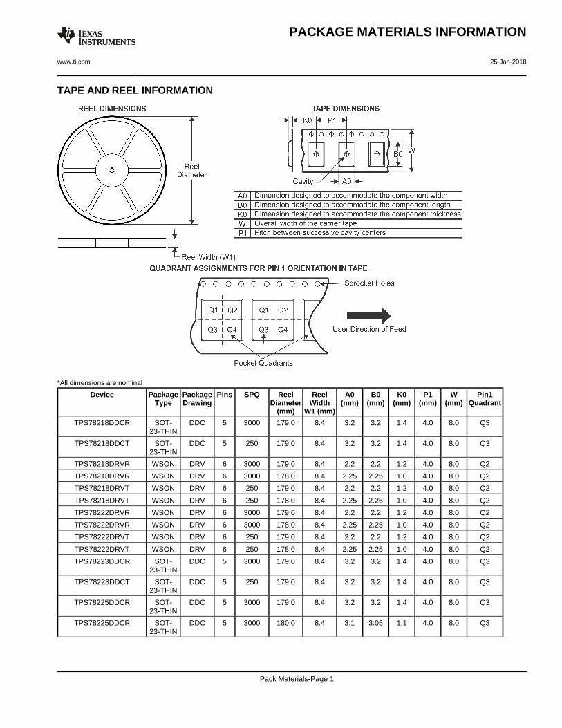
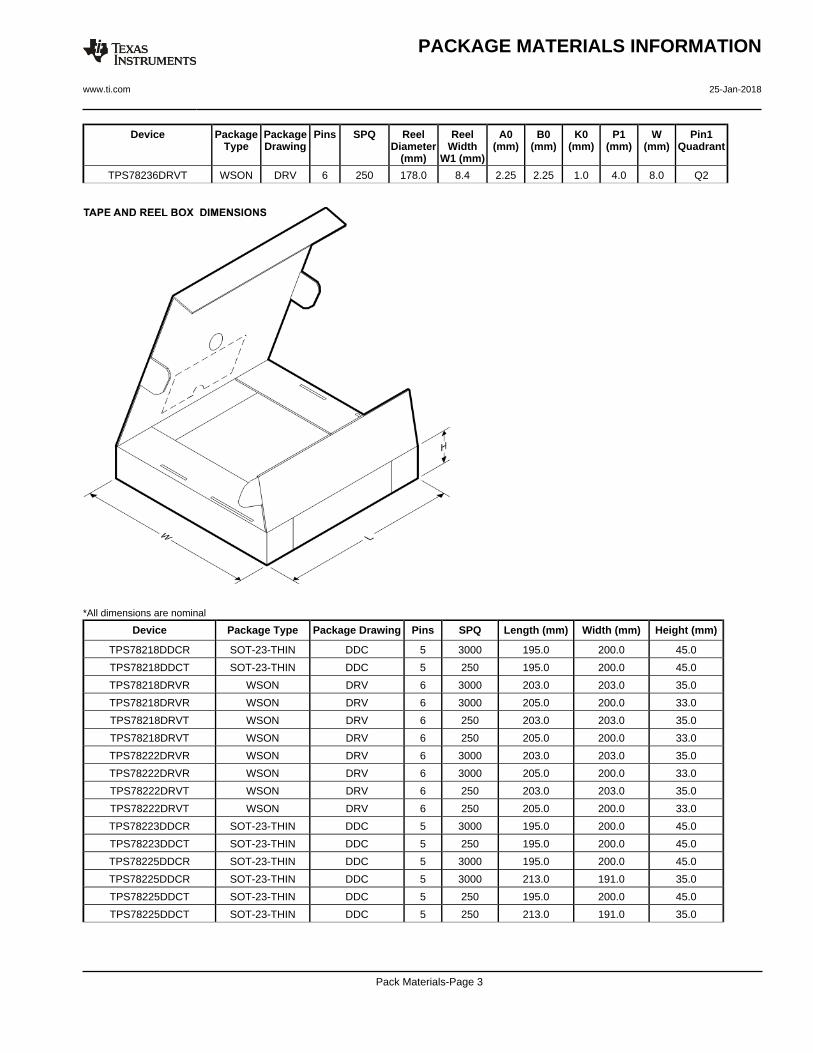
TAPE AND REEL INFORMATION
*All dimensions are nominal
Device PackageType
PackageDrawing
Pins SPQ ReelDiameter
(mm)
ReelWidth
W1 (mm)
A0(mm)
B0(mm)
K0(mm)
P1(mm)
W(mm)
Pin1Quadrant
TPS78218DDCR SOT-23-THIN
DDC 5 3000 179.0 8.4 3.2 3.2 1.4 4.0 8.0 Q3
TPS78218DDCT SOT-23-THIN
DDC 5 250 179.0 8.4 3.2 3.2 1.4 4.0 8.0 Q3
TPS78218DRVR WSON DRV 6 3000 179.0 8.4 2.2 2.2 1.2 4.0 8.0 Q2
TPS78218DRVR WSON DRV 6 3000 178.0 8.4 2.25 2.25 1.0 4.0 8.0 Q2
TPS78218DRVT WSON DRV 6 250 179.0 8.4 2.2 2.2 1.2 4.0 8.0 Q2
TPS78218DRVT WSON DRV 6 250 178.0 8.4 2.25 2.25 1.0 4.0 8.0 Q2
TPS78222DRVR WSON DRV 6 3000 179.0 8.4 2.2 2.2 1.2 4.0 8.0 Q2
TPS78222DRVR WSON DRV 6 3000 178.0 8.4 2.25 2.25 1.0 4.0 8.0 Q2
TPS78222DRVT WSON DRV 6 250 179.0 8.4 2.2 2.2 1.2 4.0 8.0 Q2
TPS78222DRVT WSON DRV 6 250 178.0 8.4 2.25 2.25 1.0 4.0 8.0 Q2
TPS78223DDCR SOT-23-THIN
DDC 5 3000 179.0 8.4 3.2 3.2 1.4 4.0 8.0 Q3
TPS78223DDCT SOT-23-THIN
DDC 5 250 179.0 8.4 3.2 3.2 1.4 4.0 8.0 Q3
TPS78225DDCR SOT-23-THIN
DDC 5 3000 179.0 8.4 3.2 3.2 1.4 4.0 8.0 Q3
TPS78225DDCR SOT-23-THIN
DDC 5 3000 180.0 8.4 3.1 3.05 1.1 4.0 8.0 Q3
PACKAGE MATERIALS INFORMATION
www.ti.com 25-Jan-2018
Pack Materials-Page 1
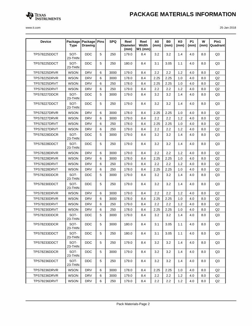
Device PackageType
PackageDrawing
Pins SPQ ReelDiameter
(mm)
ReelWidth
W1 (mm)
A0(mm)
B0(mm)
K0(mm)
P1(mm)
W(mm)
Pin1Quadrant
TPS78225DDCT SOT-23-THIN
DDC 5 250 179.0 8.4 3.2 3.2 1.4 4.0 8.0 Q3
TPS78225DDCT SOT-23-THIN
DDC 5 250 180.0 8.4 3.1 3.05 1.1 4.0 8.0 Q3
TPS78225DRVR WSON DRV 6 3000 179.0 8.4 2.2 2.2 1.2 4.0 8.0 Q2
TPS78225DRVR WSON DRV 6 3000 178.0 8.4 2.25 2.25 1.0 4.0 8.0 Q2
TPS78225DRVT WSON DRV 6 250 178.0 8.4 2.25 2.25 1.0 4.0 8.0 Q2
TPS78225DRVT WSON DRV 6 250 179.0 8.4 2.2 2.2 1.2 4.0 8.0 Q2
TPS78227DDCR SOT-23-THIN
DDC 5 3000 179.0 8.4 3.2 3.2 1.4 4.0 8.0 Q3
TPS78227DDCT SOT-23-THIN
DDC 5 250 179.0 8.4 3.2 3.2 1.4 4.0 8.0 Q3
TPS78227DRVR WSON DRV 6 3000 178.0 8.4 2.25 2.25 1.0 4.0 8.0 Q2
TPS78227DRVR WSON DRV 6 3000 179.0 8.4 2.2 2.2 1.2 4.0 8.0 Q2
TPS78227DRVT WSON DRV 6 250 178.0 8.4 2.25 2.25 1.0 4.0 8.0 Q2
TPS78227DRVT WSON DRV 6 250 179.0 8.4 2.2 2.2 1.2 4.0 8.0 Q2
TPS78228DDCR SOT-23-THIN
DDC 5 3000 179.0 8.4 3.2 3.2 1.4 4.0 8.0 Q3
TPS78228DDCT SOT-23-THIN
DDC 5 250 179.0 8.4 3.2 3.2 1.4 4.0 8.0 Q3
TPS78228DRVR WSON DRV 6 3000 179.0 8.4 2.2 2.2 1.2 4.0 8.0 Q2
TPS78228DRVR WSON DRV 6 3000 178.0 8.4 2.25 2.25 1.0 4.0 8.0 Q2
TPS78228DRVT WSON DRV 6 250 179.0 8.4 2.2 2.2 1.2 4.0 8.0 Q2
TPS78228DRVT WSON DRV 6 250 178.0 8.4 2.25 2.25 1.0 4.0 8.0 Q2
TPS78230DDCR SOT-23-THIN
DDC 5 3000 179.0 8.4 3.2 3.2 1.4 4.0 8.0 Q3
TPS78230DDCT SOT-23-THIN
DDC 5 250 179.0 8.4 3.2 3.2 1.4 4.0 8.0 Q3
TPS78230DRVR WSON DRV 6 3000 179.0 8.4 2.2 2.2 1.2 4.0 8.0 Q2
TPS78230DRVR WSON DRV 6 3000 178.0 8.4 2.25 2.25 1.0 4.0 8.0 Q2
TPS78230DRVT WSON DRV 6 250 179.0 8.4 2.2 2.2 1.2 4.0 8.0 Q2
TPS78230DRVT WSON DRV 6 250 178.0 8.4 2.25 2.25 1.0 4.0 8.0 Q2
TPS78233DDCR SOT-23-THIN
DDC 5 3000 179.0 8.4 3.2 3.2 1.4 4.0 8.0 Q3
TPS78233DDCR SOT-23-THIN
DDC 5 3000 180.0 8.4 3.1 3.05 1.1 4.0 8.0 Q3
TPS78233DDCT SOT-23-THIN
DDC 5 250 180.0 8.4 3.1 3.05 1.1 4.0 8.0 Q3
TPS78233DDCT SOT-23-THIN
DDC 5 250 179.0 8.4 3.2 3.2 1.4 4.0 8.0 Q3
TPS78236DDCR SOT-23-THIN
DDC 5 3000 179.0 8.4 3.2 3.2 1.4 4.0 8.0 Q3
TPS78236DDCT SOT-23-THIN
DDC 5 250 179.0 8.4 3.2 3.2 1.4 4.0 8.0 Q3
TPS78236DRVR WSON DRV 6 3000 178.0 8.4 2.25 2.25 1.0 4.0 8.0 Q2
TPS78236DRVR WSON DRV 6 3000 179.0 8.4 2.2 2.2 1.2 4.0 8.0 Q2
TPS78236DRVT WSON DRV 6 250 179.0 8.4 2.2 2.2 1.2 4.0 8.0 Q2
PACKAGE MATERIALS INFORMATION
www.ti.com 25-Jan-2018
Pack Materials-Page 2
Device PackageType
PackageDrawing
Pins SPQ ReelDiameter
(mm)
ReelWidth
W1 (mm)
A0(mm)
B0(mm)
K0(mm)
P1(mm)
W(mm)
Pin1Quadrant
TPS78236DRVT WSON DRV 6 250 178.0 8.4 2.25 2.25 1.0 4.0 8.0 Q2
*All dimensions are nominal
Device Package Type Package Drawing Pins SPQ Length (mm) Width (mm) Height (mm)
TPS78218DDCR SOT-23-THIN DDC 5 3000 195.0 200.0 45.0
TPS78218DDCT SOT-23-THIN DDC 5 250 195.0 200.0 45.0
TPS78218DRVR WSON DRV 6 3000 203.0 203.0 35.0
TPS78218DRVR WSON DRV 6 3000 205.0 200.0 33.0
TPS78218DRVT WSON DRV 6 250 203.0 203.0 35.0
TPS78218DRVT WSON DRV 6 250 205.0 200.0 33.0
TPS78222DRVR WSON DRV 6 3000 203.0 203.0 35.0
TPS78222DRVR WSON DRV 6 3000 205.0 200.0 33.0
TPS78222DRVT WSON DRV 6 250 203.0 203.0 35.0
TPS78222DRVT WSON DRV 6 250 205.0 200.0 33.0
TPS78223DDCR SOT-23-THIN DDC 5 3000 195.0 200.0 45.0
TPS78223DDCT SOT-23-THIN DDC 5 250 195.0 200.0 45.0
TPS78225DDCR SOT-23-THIN DDC 5 3000 195.0 200.0 45.0
TPS78225DDCR SOT-23-THIN DDC 5 3000 213.0 191.0 35.0
TPS78225DDCT SOT-23-THIN DDC 5 250 195.0 200.0 45.0
TPS78225DDCT SOT-23-THIN DDC 5 250 213.0 191.0 35.0
PACKAGE MATERIALS INFORMATION
www.ti.com 25-Jan-2018
Pack Materials-Page 3

Device Package Type Package Drawing Pins SPQ Length (mm) Width (mm) Height (mm)
TPS78225DRVR WSON DRV 6 3000 203.0 203.0 35.0
TPS78225DRVR WSON DRV 6 3000 205.0 200.0 33.0
TPS78225DRVT WSON DRV 6 250 205.0 200.0 33.0
TPS78225DRVT WSON DRV 6 250 203.0 203.0 35.0
TPS78227DDCR SOT-23-THIN DDC 5 3000 195.0 200.0 45.0
TPS78227DDCT SOT-23-THIN DDC 5 250 195.0 200.0 45.0
TPS78227DRVR WSON DRV 6 3000 205.0 200.0 33.0
TPS78227DRVR WSON DRV 6 3000 203.0 203.0 35.0
TPS78227DRVT WSON DRV 6 250 205.0 200.0 33.0
TPS78227DRVT WSON DRV 6 250 203.0 203.0 35.0
TPS78228DDCR SOT-23-THIN DDC 5 3000 195.0 200.0 45.0
TPS78228DDCT SOT-23-THIN DDC 5 250 195.0 200.0 45.0
TPS78228DRVR WSON DRV 6 3000 203.0 203.0 35.0
TPS78228DRVR WSON DRV 6 3000 205.0 200.0 33.0
TPS78228DRVT WSON DRV 6 250 203.0 203.0 35.0
TPS78228DRVT WSON DRV 6 250 205.0 200.0 33.0
TPS78230DDCR SOT-23-THIN DDC 5 3000 195.0 200.0 45.0
TPS78230DDCT SOT-23-THIN DDC 5 250 195.0 200.0 45.0
TPS78230DRVR WSON DRV 6 3000 203.0 203.0 35.0
TPS78230DRVR WSON DRV 6 3000 205.0 200.0 33.0
TPS78230DRVT WSON DRV 6 250 203.0 203.0 35.0
TPS78230DRVT WSON DRV 6 250 205.0 200.0 33.0
TPS78233DDCR SOT-23-THIN DDC 5 3000 195.0 200.0 45.0
TPS78233DDCR SOT-23-THIN DDC 5 3000 213.0 191.0 35.0
TPS78233DDCT SOT-23-THIN DDC 5 250 213.0 191.0 35.0
TPS78233DDCT SOT-23-THIN DDC 5 250 195.0 200.0 45.0
TPS78236DDCR SOT-23-THIN DDC 5 3000 195.0 200.0 45.0
TPS78236DDCT SOT-23-THIN DDC 5 250 195.0 200.0 45.0
TPS78236DRVR WSON DRV 6 3000 205.0 200.0 33.0
TPS78236DRVR WSON DRV 6 3000 203.0 203.0 35.0
TPS78236DRVT WSON DRV 6 250 203.0 203.0 35.0
TPS78236DRVT WSON DRV 6 250 205.0 200.0 33.0
PACKAGE MATERIALS INFORMATION
www.ti.com 25-Jan-2018
Pack Materials-Page 4

GENERIC PACKAGE VIEW
Images above are just a representation of the package family, actual package may vary.Refer to the product data sheet for package details.
DRV 6 WSON - 0.8 mm max heightPLASTIC SMALL OUTLINE - NO LEAD
4206925/F
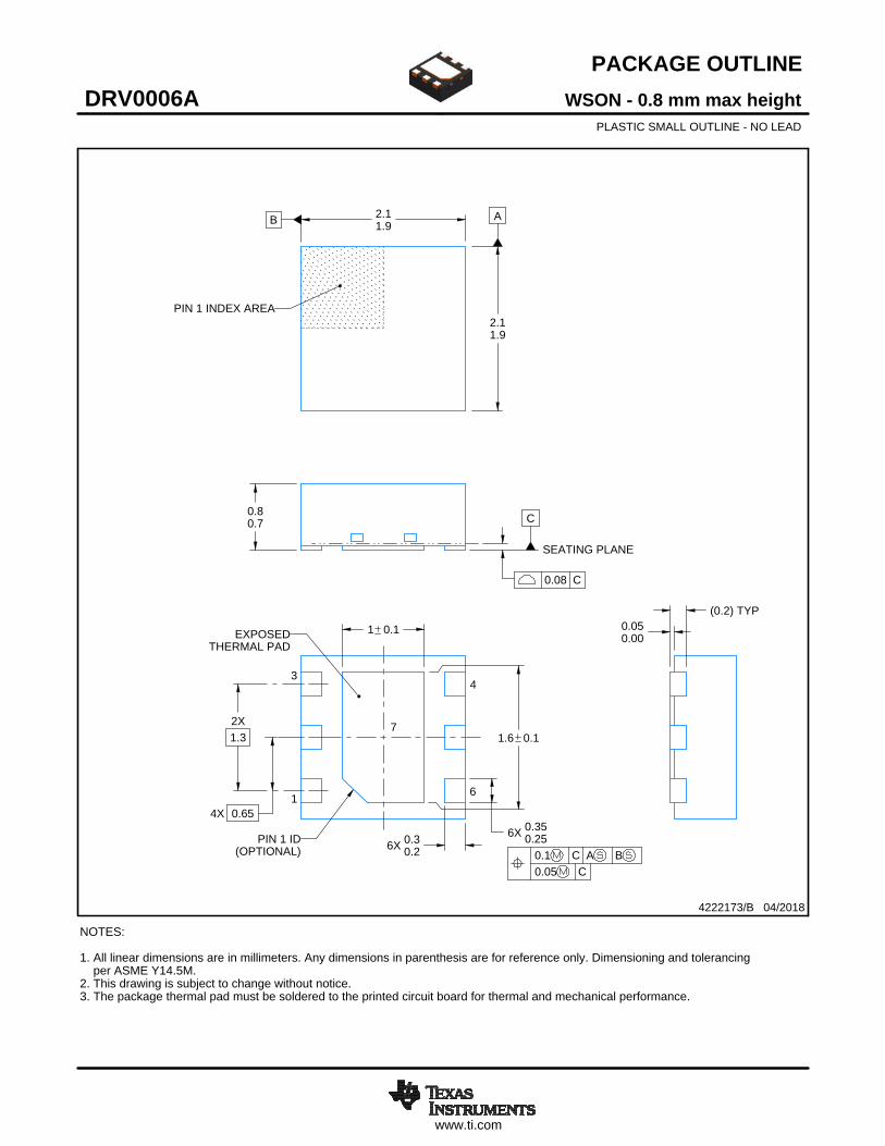
www.ti.com
PACKAGE OUTLINE
C
6X 0.350.25
1.6 0.1
6X 0.30.2
2X1.3
1 0.1
4X 0.65
0.80.7
0.050.00
B 2.11.9
A
2.11.9
(0.2) TYP
WSON - 0.8 mm max heightDRV0006APLASTIC SMALL OUTLINE - NO LEAD
4222173/B 04/2018
PIN 1 INDEX AREA
SEATING PLANE
0.08 C
1
34
6
(OPTIONAL)PIN 1 ID
0.1 C A B0.05 C
THERMAL PADEXPOSED
7
NOTES: 1. All linear dimensions are in millimeters. Any dimensions in parenthesis are for reference only. Dimensioning and tolerancing per ASME Y14.5M. 2. This drawing is subject to change without notice. 3. The package thermal pad must be soldered to the printed circuit board for thermal and mechanical performance.
SCALE 5.500

www.ti.com
EXAMPLE BOARD LAYOUT
0.07 MINALL AROUND
0.07 MAXALL AROUND
(1)
4X (0.65)
(1.95)
6X (0.3)
6X (0.45)
(1.6)
(R0.05) TYP
( 0.2) VIATYP
(1.1)
WSON - 0.8 mm max heightDRV0006APLASTIC SMALL OUTLINE - NO LEAD
4222173/B 04/2018
SYMM
1
34
6
SYMM
LAND PATTERN EXAMPLESCALE:25X
7
NOTES: (continued) 4. This package is designed to be soldered to a thermal pad on the board. For more information, see Texas Instruments literature number SLUA271 (www.ti.com/lit/slua271).5. Vias are optional depending on application, refer to device data sheet. If some or all are implemented, recommended via locations are shown.
SOLDER MASKOPENINGSOLDER MASK
METAL UNDER
SOLDER MASKDEFINED
METALSOLDER MASKOPENING
SOLDER MASK DETAILS
NON SOLDER MASKDEFINED
(PREFERRED)
www.ti.com
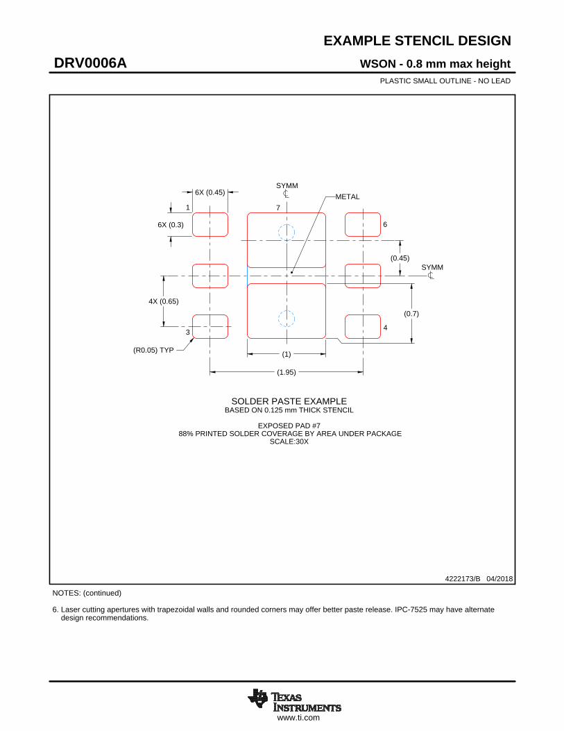
EXAMPLE STENCIL DESIGN
6X (0.3)
6X (0.45)
4X (0.65)
(0.7)
(1)
(1.95)
(R0.05) TYP
(0.45)
WSON - 0.8 mm max heightDRV0006APLASTIC SMALL OUTLINE - NO LEAD
4222173/B 04/2018
NOTES: (continued) 6. Laser cutting apertures with trapezoidal walls and rounded corners may offer better paste release. IPC-7525 may have alternate design recommendations.
SOLDER PASTE EXAMPLEBASED ON 0.125 mm THICK STENCIL
EXPOSED PAD #7
88% PRINTED SOLDER COVERAGE BY AREA UNDER PACKAGESCALE:30X
SYMM
1
3 4
6
SYMM
METAL7
IMPORTANT NOTICE
Texas Instruments Incorporated (TI) reserves the right to make corrections, enhancements, improvements and other changes to itssemiconductor products and services per JESD46, latest issue, and to discontinue any product or service per JESD48, latest issue. Buyersshould obtain the latest relevant information before placing orders and should verify that such information is current and complete.TI’s published terms of sale for semiconductor products (http://www.ti.com/sc/docs/stdterms.htm) apply to the sale of packaged integratedcircuit products that TI has qualified and released to market. Additional terms may apply to the use or sale of other types of TI products andservices.Reproduction of significant portions of TI information in TI data sheets is permissible only if reproduction is without alteration and isaccompanied by all associated warranties, conditions, limitations, and notices. TI is not responsible or liable for such reproduceddocumentation. Information of third parties may be subject to additional restrictions. Resale of TI products or services with statementsdifferent from or beyond the parameters stated by TI for that product or service voids all express and any implied warranties for theassociated TI product or service and is an unfair and deceptive business practice. TI is not responsible or liable for any such statements.Buyers and others who are developing systems that incorporate TI products (collectively, “Designers”) understand and agree that Designersremain responsible for using their independent analysis, evaluation and judgment in designing their applications and that Designers havefull and exclusive responsibility to assure the safety of Designers' applications and compliance of their applications (and of all TI productsused in or for Designers’ applications) with all applicable regulations, laws and other applicable requirements. Designer represents that, withrespect to their applications, Designer has all the necessary expertise to create and implement safeguards that (1) anticipate dangerousconsequences of failures, (2) monitor failures and their consequences, and (3) lessen the likelihood of failures that might cause harm andtake appropriate actions. Designer agrees that prior to using or distributing any applications that include TI products, Designer willthoroughly test such applications and the functionality of such TI products as used in such applications.TI’s provision of technical, application or other design advice, quality characterization, reliability data or other services or information,including, but not limited to, reference designs and materials relating to evaluation modules, (collectively, “TI Resources”) are intended toassist designers who are developing applications that incorporate TI products; by downloading, accessing or using TI Resources in anyway, Designer (individually or, if Designer is acting on behalf of a company, Designer’s company) agrees to use any particular TI Resourcesolely for this purpose and subject to the terms of this Notice.TI’s provision of TI Resources does not expand or otherwise alter TI’s applicable published warranties or warranty disclaimers for TIproducts, and no additional obligations or liabilities arise from TI providing such TI Resources. TI reserves the right to make corrections,enhancements, improvements and other changes to its TI Resources. TI has not conducted any testing other than that specificallydescribed in the published documentation for a particular TI Resource.Designer is authorized to use, copy and modify any individual TI Resource only in connection with the development of applications thatinclude the TI product(s) identified in such TI Resource. NO OTHER LICENSE, EXPRESS OR IMPLIED, BY ESTOPPEL OR OTHERWISETO ANY OTHER TI INTELLECTUAL PROPERTY RIGHT, AND NO LICENSE TO ANY TECHNOLOGY OR INTELLECTUAL PROPERTYRIGHT OF TI OR ANY THIRD PARTY IS GRANTED HEREIN, including but not limited to any patent right, copyright, mask work right, orother intellectual property right relating to any combination, machine, or process in which TI products or services are used. Informationregarding or referencing third-party products or services does not constitute a license to use such products or services, or a warranty orendorsement thereof. Use of TI Resources may require a license from a third party under the patents or other intellectual property of thethird party, or a license from TI under the patents or other intellectual property of TI.TI RESOURCES ARE PROVIDED “AS IS” AND WITH ALL FAULTS. TI DISCLAIMS ALL OTHER WARRANTIES ORREPRESENTATIONS, EXPRESS OR IMPLIED, REGARDING RESOURCES OR USE THEREOF, INCLUDING BUT NOT LIMITED TOACCURACY OR COMPLETENESS, TITLE, ANY EPIDEMIC FAILURE WARRANTY AND ANY IMPLIED WARRANTIES OFMERCHANTABILITY, FITNESS FOR A PARTICULAR PURPOSE, AND NON-INFRINGEMENT OF ANY THIRD PARTY INTELLECTUALPROPERTY RIGHTS. TI SHALL NOT BE LIABLE FOR AND SHALL NOT DEFEND OR INDEMNIFY DESIGNER AGAINST ANY CLAIM,INCLUDING BUT NOT LIMITED TO ANY INFRINGEMENT CLAIM THAT RELATES TO OR IS BASED ON ANY COMBINATION OFPRODUCTS EVEN IF DESCRIBED IN TI RESOURCES OR OTHERWISE. IN NO EVENT SHALL TI BE LIABLE FOR ANY ACTUAL,DIRECT, SPECIAL, COLLATERAL, INDIRECT, PUNITIVE, INCIDENTAL, CONSEQUENTIAL OR EXEMPLARY DAMAGES INCONNECTION WITH OR ARISING OUT OF TI RESOURCES OR USE THEREOF, AND REGARDLESS OF WHETHER TI HAS BEENADVISED OF THE POSSIBILITY OF SUCH DAMAGES.Unless TI has explicitly designated an individual product as meeting the requirements of a particular industry standard (e.g., ISO/TS 16949and ISO 26262), TI is not responsible for any failure to meet such industry standard requirements.Where TI specifically promotes products as facilitating functional safety or as compliant with industry functional safety standards, suchproducts are intended to help enable customers to design and create their own applications that meet applicable functional safety standardsand requirements. Using products in an application does not by itself establish any safety features in the application. Designers mustensure compliance with safety-related requirements and standards applicable to their applications. Designer may not use any TI products inlife-critical medical equipment unless authorized officers of the parties have executed a special contract specifically governing such use.Life-critical medical equipment is medical equipment where failure of such equipment would cause serious bodily injury or death (e.g., lifesupport, pacemakers, defibrillators, heart pumps, neurostimulators, and implantables). Such equipment includes, without limitation, allmedical devices identified by the U.S. Food and Drug Administration as Class III devices and equivalent classifications outside the U.S.TI may expressly designate certain products as completing a particular qualification (e.g., Q100, Military Grade, or Enhanced Product).Designers agree that it has the necessary expertise to select the product with the appropriate qualification designation for their applicationsand that proper product selection is at Designers’ own risk. Designers are solely responsible for compliance with all legal and regulatoryrequirements in connection with such selection.Designer will fully indemnify TI and its representatives against any damages, costs, losses, and/or liabilities arising out of Designer’s non-compliance with the terms and provisions of this Notice.
Mailing Address: Texas Instruments, Post Office Box 655303, Dallas, Texas 75265Copyright © 2018, Texas Instruments Incorporated