secure electromagnetic buildings using slow phase
TRANSCRIPT

This is a repository copy of Secure Electromagnetic Buildings Using Slow Phase Switching Frequency Selective Surfaces.
White Rose Research Online URL for this paper:http://eprints.whiterose.ac.uk/91770/
Version: Accepted Version
Article:
Roberts, J., Ford, K.L. and Rigelsford, J.M. (2016) Secure Electromagnetic Buildings Using Slow Phase Switching Frequency Selective Surfaces. IEEE Transactions on Antennas and Propagation, 64 (1). pp. 251-261. ISSN 0018-926X
https://doi.org/10.1109/TAP.2015.2499773
[email protected]://eprints.whiterose.ac.uk/
Reuse
Unless indicated otherwise, fulltext items are protected by copyright with all rights reserved. The copyright exception in section 29 of the Copyright, Designs and Patents Act 1988 allows the making of a single copy solely for the purpose of non-commercial research or private study within the limits of fair dealing. The publisher or other rights-holder may allow further reproduction and re-use of this version - refer to the White Rose Research Online record for this item. Where records identify the publisher as the copyright holder, users can verify any specific terms of use on the publisher’s website.
Takedown
If you consider content in White Rose Research Online to be in breach of UK law, please notify us by emailing [email protected] including the URL of the record and the reason for the withdrawal request.
1
Abstract—The concept of a secure electromagnetic building
which can successfully prohibit wireless communications is presented. Wireless security is achieved using a slow phase switching technique and can be realized by time varying the transmission properties of a frequency selective surface to increase the bit error rate of the unwanted signal. Results are presented which demonstrate that a technique of phase switching at rates much lower than the baseband data rate can be used successfully. The system has been implemented using a reconfigurable dual polarized dual layer frequency selective surface incorporating varactor diodes where over 100° of phase change can be achieved for voltage changes of ±0–3V. A vector signal analyzer was used to evaluate the bit error rate performance of the system for a GSM signal operating at 2GHz. Bit error rates are shown to be as high as 36% which are sufficient to successfully prohibit wireless communication. The solution is also shown to be robust over a wide range of incidence angles which is important for real world applications where the location of the prohibited wireless source may be unknown or mobile. Furthermore, as the system is reconfigurable the building can be switched between a secure and non-secure mode.
Index Terms—Frequency Selective Surfaces
I. INTRODUCTION
The proliferation of wireless communication devices is increasing globally which brings about the demand for increased signal coverage, network capacity and user quality of service, particularly in densely populated areas. However, there are applications where it may be appropriate to block or shield communications such as in prisons, military buildings, embassies, and hospitals etc. The common approach to blocking communications is to use jamming or shielding techniques. Jamming is an effective and well established method, however, these techniques can be illegal in some countries and may also have an impact on legitimate users who are unintentionally jammed. Shielding is also simple in theory but can be difficult to achieve in practice particularly in high signal coverage areas, due to the very high attenuation levels that may be required to effectively block a communications signal. An example of a problematic application was identified in a previous study of UK prisons, [1], which found that a high percentage of prisons were
The authors are with the Communications Group, Department of
Electronic and Electrical Engineering, University of Sheffield, Sheffield, S1 3JD, UK. (e-mail: [email protected])
classified as having very good or excellent cellular signal coverage due to the locations in urban areas. In this situation jamming or shielding may not be appropriate.
In the research community these application areas lend themselves to Frequency Selective Surface (FSS) solutions. FSS are a class of meta-material or meta-surface which have electromagnetic properties which cannot be found using a bulk dielectric or magnetic material. An FSS uses periodic arrays of metallic or dielectric elements to provide frequency dependent transmission and reflection properties [2]. There has been a significant amount of research relating to FSS over a number of decades and the use of FSS in building applications is a relatively substantial research area. FSS studies have been applied to wireless communications applications, for instance to reduce indoor interference [3]–[10]. There has also been significant research into reconfigurable FSS which could have applications for smart buildings [11]–[20] and miniaturized FSS design which would be particularly applicable for low frequency in-building communications applications [21]–[24]. Work has also been carried out on reconfigurable systems using pumped RF structures for physical layer security [25].
The application of stopping or blocking communications signals through the use of FSS is more problematic, particularly in high signal strength areas due to the high sensitivity of modern mobile receivers which can operate with powers as low as -120dBm or less. The aim of this paper is to develop a reconfigurable FSS system that can be used to impair a communications signal for indoor-outdoor or indoor-indoor building applications which adds significantly to an initial demonstration of the technique presented in [26]. The remainder of the paper sets out the fundamental concept, system simulations, application specific implications, FSS design and practical demonstration of the proposed system.
II. SECURE ELECTROMAGNETIC BUILDING CONCEPT
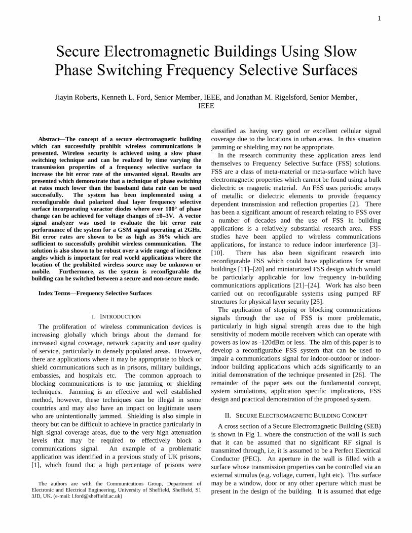
A cross section of a Secure Electromagnetic Building (SEB) is shown in Fig 1. where the construction of the wall is such that it can be assumed that no significant RF signal is transmitted through, i.e, it is assumed to be a Perfect Electrical Conductor (PEC). An aperture in the wall is filled with a surface whose transmission properties can be controlled via an external stimulus (e.g. voltage, current, light etc). This surface may be a window, door or any other aperture which must be present in the design of the building. It is assumed that edge
Secure Electromagnetic Buildings Using Slow Phase Switching Frequency Selective Surfaces Jiayin Roberts, Kenneth L. Ford, Senior Member, IEEE, and Jonathan M. Rigelsford, Senior Member,
IEEE
2
diffractions are not a significant contributor to the fields transmitted through the structure.
Figure 1: Illustration of SEB
Assuming that the surface is much larger than the
wavelength of the incoming electromagnetic plane wave, the transmission coefficient is given by Eq. 1: 酵岫建 肯岻 噺 】酵岫建 肯岻】結珍笛岫痛提岻 (1)
where t, is the complex transmission coefficient, (t,) is the phase of the transmission coefficient, is the angle of incidence and t is time. The transmission coefficient will also vary as a function of the polarization of the incoming plane wave. The following sections will show two modes of operation where the transmission phase varies with time, namely, Fast Phase Switching (FPS) and Slow Phase Switching (SPS).
A. Fast phase switching
Consider the case where the transmission coefficient is varied between two states in a time, T, as described in Eq. (2) and assume a normal incidence plane-wave illumination for simplicity. Phase state “1” occurs for a time T-t and phase state “2” occurs for a time t. 酵岫建岻 噺 】酵怠】結珍笛迭 ど 隼 建 隼 劇 伐 つ建 酵岫建岻 噺 】酵態】結珍笛鉄 劇 伐 つ建 隼 建 隼 劇 (2)
Assuming that the states are switched periodically then the transmission coefficient can be analyzed using a Fourier series as shown in Eq. (3).
n
tjnnect 0)( (3)
where 0=2/T and the Fourier coefficient cn is given by Eq. (4) for n>0. c0 is the mean value of the transmission coefficient over the period, T.
T
tjnn dtet
Tc
0
0)(1 (4)
Solving (4) yields the result given in (5).
T
tnjj
T
tnjj
n
ee
ee
n
jc
2
2
2
1
1
1
22
1
(5)
The Fourier transform of (3) yields the classic response of an infinite sum of weighted impulses spaced n0 apart. It is clear that the frequency spectrum of the transmission coefficient will be dependent on the magnitude of the transmission coefficient, the phase difference between the two switching states, the duty cycle of the switching waveform and the switching period.
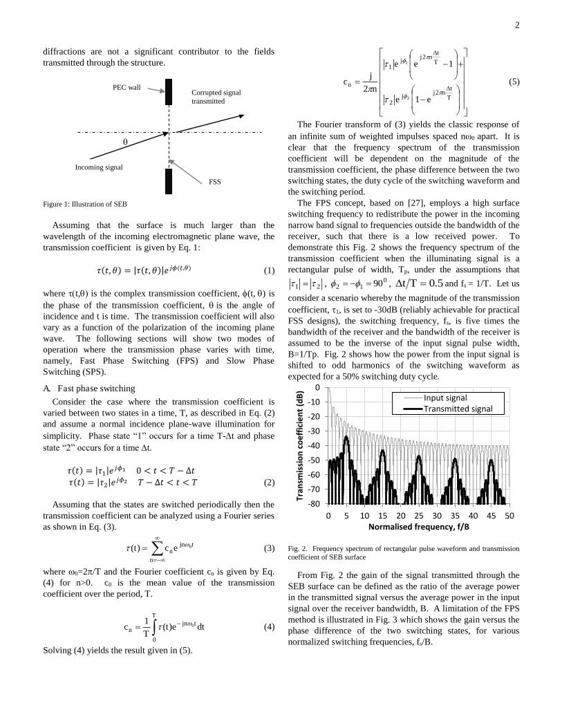
The FPS concept, based on [27], employs a high surface switching frequency to redistribute the power in the incoming narrow band signal to frequencies outside the bandwidth of the receiver, such that there is a low received power. To demonstrate this Fig. 2 shows the frequency spectrum of the transmission coefficient when the illuminating signal is a rectangular pulse of width, Tp, under the assumptions that
21 , 012 90 , 5.0 Tt and fs = 1/T. Let us
consider a scenario whereby the magnitude of the transmission coefficient, 1, is set to -30dB (reliably achievable for practical FSS designs), the switching frequency, fs, is five times the bandwidth of the receiver and the bandwidth of the receiver is assumed to be the inverse of the input signal pulse width, B=1/Tp. Fig. 2 shows how the power from the input signal is shifted to odd harmonics of the switching waveform as expected for a 50% switching duty cycle.
Fig. 2. Frequency spectrum of rectangular pulse waveform and transmission coefficient of SEB surface
From Fig. 2 the gain of the signal transmitted through the SEB surface can be defined as the ratio of the average power in the transmitted signal versus the average power in the input signal over the receiver bandwidth, B. A limitation of the FPS method is illustrated in Fig. 3 which shows the gain versus the phase difference of the two switching states, for various normalized switching frequencies, fs/B.
-80
-70
-60
-50
-40
-30
-20
-10
0
0 5 10 15 20 25 30 35 40 45 50
Tra
nsm
issi
on
co
eff
icie
nt
(dB
)
Normalised frequency, f/B
Input signal
Transmitted signal
Incoming signal
PEC wall Corrupted signal transmitted
FSS
3
Fig. 3. Gain of transmitted signal
It can be seen from Fig. 3 that beyond the passive
transmission response of the SEB surface, an extra attenuation of between 10 and 25 dB is achieved. The practical implications on a system where the signal attenuation may have to be >70dB will require a very high surface transmission loss, a high switching frequency and a high phase difference. All of these quantities are achievable in theory, and some in practice, however, to be able to achieve these requirements for a wide range of incidence angles and polarizations may difficult. As such the following section details an alternative novel method of signal impairment.
B. Slow phase switching
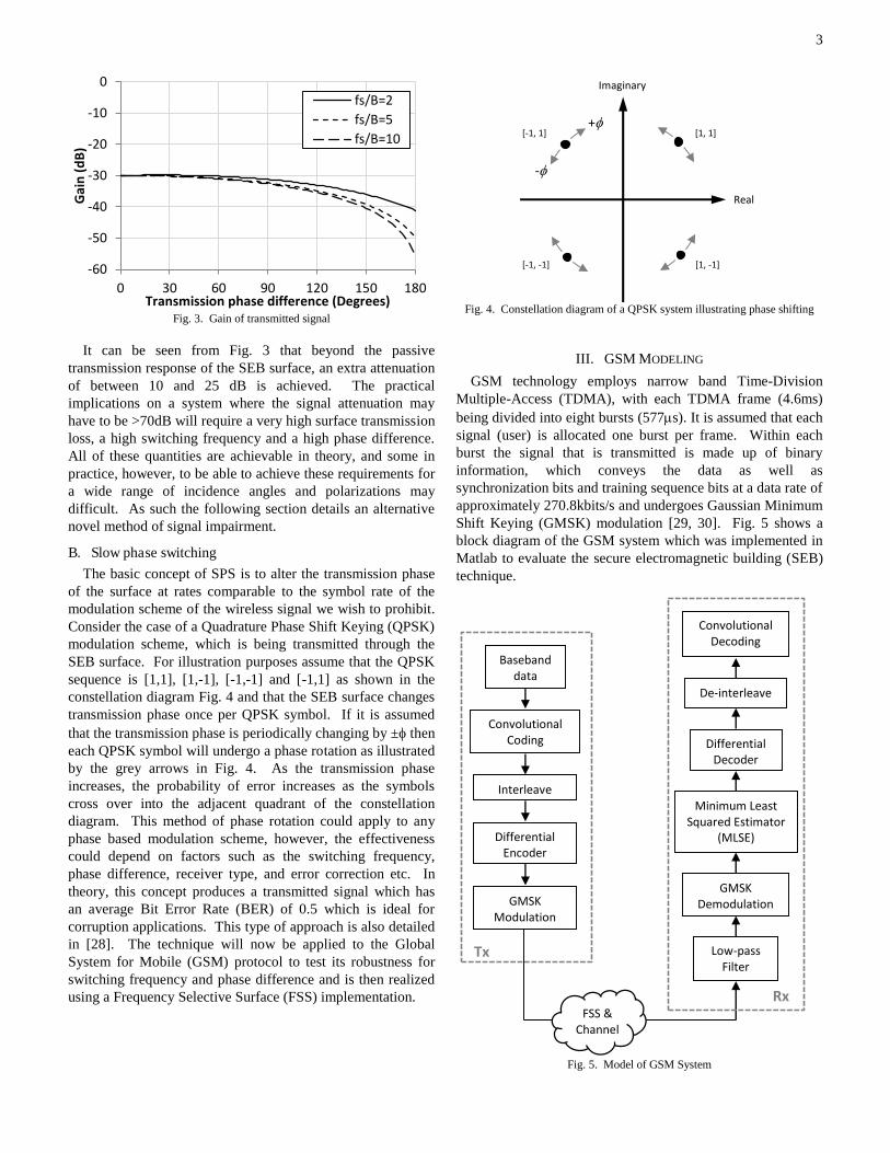
The basic concept of SPS is to alter the transmission phase of the surface at rates comparable to the symbol rate of the modulation scheme of the wireless signal we wish to prohibit. Consider the case of a Quadrature Phase Shift Keying (QPSK) modulation scheme, which is being transmitted through the SEB surface. For illustration purposes assume that the QPSK sequence is [1,1], [1,-1], [-1,-1] and [-1,1] as shown in the constellation diagram Fig. 4 and that the SEB surface changes transmission phase once per QPSK symbol. If it is assumed that the transmission phase is periodically changing by ± then each QPSK symbol will undergo a phase rotation as illustrated by the grey arrows in Fig. 4. As the transmission phase increases, the probability of error increases as the symbols cross over into the adjacent quadrant of the constellation diagram. This method of phase rotation could apply to any phase based modulation scheme, however, the effectiveness could depend on factors such as the switching frequency, phase difference, receiver type, and error correction etc. In theory, this concept produces a transmitted signal which has an average Bit Error Rate (BER) of 0.5 which is ideal for corruption applications. This type of approach is also detailed in [28]. The technique will now be applied to the Global System for Mobile (GSM) protocol to test its robustness for switching frequency and phase difference and is then realized using a Frequency Selective Surface (FSS) implementation.
Fig. 4. Constellation diagram of a QPSK system illustrating phase shifting
III. GSM MODELING
GSM technology employs narrow band Time-Division Multiple-Access (TDMA), with each TDMA frame (4.6ms) being divided into eight bursts (577s). It is assumed that each signal (user) is allocated one burst per frame. Within each burst the signal that is transmitted is made up of binary information, which conveys the data as well as synchronization bits and training sequence bits at a data rate of approximately 270.8kbits/s and undergoes Gaussian Minimum Shift Keying (GMSK) modulation [29, 30]. Fig. 5 shows a block diagram of the GSM system which was implemented in Matlab to evaluate the secure electromagnetic building (SEB) technique.
Fig. 5. Model of GSM System
-60
-50
-40
-30
-20
-10
0
0 30 60 90 120 150 180
Ga
in (
dB
)
Transmission phase difference (Degrees)
fs/B=2
fs/B=5
fs/B=10
[-1, -1]
Real
Imaginary
[1, 1]
[1, -1]
[-1, 1]
-
+
Differential
Encoder
GMSK
Modulation
Baseband
data
Convolutional
Coding
Interleave
Minimum Least
Squared Estimator
(MLSE)
Differential
Decoder
De-interleave
Convolutional
Decoding
Low-pass
Filter
GMSK
Demodulation
Tx
Rx FSS &
Channel

4
The GSM protocol assumes that the channel in which the signal is propagating through remains relatively constant with time, to assist in channel estimation, so if the channel response can be impaired appropriately with use of an FSS it should be possible to corrupt the signal. As in the previous scenarios, for simplicity it is assumed that the FSS transmission response will vary periodically at a switching frequency, fs. To simulate the FSS channel, two FSS variables were considered; Phase and Amplitude. Noise was not considered in this work so that signal impairment from only the FSS could be evaluated. For a complex GSM waveform d(t) and a complex transmission coefficient of the FSS (t) (as defined in Eq. 2), the signal after the channel can be computed as: 検岫建岻 噺 穴岫建岻酵岫建岻 (6)
The effect of this is illustrated in Fig. 6 which shows the phase of a GSM signal before and after FSS switching. The data elements of the GSM bit stream were randomly generated and each bit was oversampled by a factor of 20 to increase signal accuracy. In all examples the training sequence used was TS0 = [0 0 1 0 0 1 0 1 1 1 0 0 0 0 1 0 0 0 1 0 0 1 0 1 1 1]. A transmission coefficient of 0dB and a transmission phase switching between ±60° at a rate, fs = 271kHz was chosen for illustration purposes.
Fig. 6. GSM signal phase a) before switching, b) after phase switching at 271kHz
The impact of the switching process is clearly observed in the frequency domain, which also aids in the explanation of how low frequency switching can be advantageous to wireless
security. Fig. 7a shows the baseband frequency spectrum of the GSM signal with randomly generated data bits prior to transmission through the FSS. The amplitude is normalized to the maximum of the baseband frequency spectrum. Figs. 7b and 7c show the normalized frequency spectrum of the transmitted signal with fs=271kHz and fs=135kHz respectively each having a phase change of ±60°.
a)
b)
c) Fig. 7. Frequency Spectrum of the FSS normalized to maximum of baseband signal a) before switching b) fast switching, fs= 271KHz and c) slow
switching, fs= 135KHz
When the signal is switched at fs=271kHz, the spectrum comprises of the original baseband data plus harmonics spaced nfs kHz apart, where n is an odd integer, making the first
-180-150-120
-90-60-30
0306090
120150180
0 1000 2000 3000
Ph
ase
(D
eg
ree
s)
Sample points
-180-150-120
-90-60-30
0306090
120150180
0 1000 2000 3000
Ph
ase
(D
eg
ree
s)
Sample points
-70
-60
-50
-40
-30
-20
-10
0
-2000 -1000 0 1000 2000
No
rma
lise
d a
mp
litu
de
(d
B)
Frequency (kHz)
-70
-60
-50
-40
-30
-20
-10
0
-2000 -1000 0 1000 2000
No
rma
lise
d a
mp
litu
de
(d
B)
Frequency (kHz)
-70
-60
-50
-40
-30
-20
-10
0
-2000 -1000 0 1000 2000
No
rma
lise
d a
mp
litu
de
(d
B)
Frequency (kHz)
a)
b)

5
harmonics at 271KHz and second harmonics at 813KHz etc. In this case the attenuation of the original baseband data is approximately 50%. It is clear that a suitable filter could be used to extract the original baseband data. The broad frequency range produced by the phase switching will cause Co-Channel Interference (CCI) and Adjacent Channel Interference (ACI) and this is further addressed in Section IV.
a)
b)
c)
d)
Fig. 8. BER (%) using a filter bandwidth of a) 135kHz, b) 270kHz, c) 405kHz and d) 540kHz. To illustrate the slow phase switching (SPS) concept we can
observe the frequency spectrum, shown in Fig. 7c, which shows the transmitted signal when fs=135kHz (i.e. changing the phase once per bit). A filter will attenuate the high order frequency components, however, the lower order components will pass through the filter and could aid in data corruption producing a much more distorted signal as compared to the original spectrum in Fig. 7a. It was found that the simulated BER for this single randomly generated data set was 42%.
In order to evaluate the design space for this technique, BER simulations were carried out for varying switching frequencies, phase differences and receiver filter -3dB bandwidths. Receiver bandwidths of 135kHz, 271kHz, 405kHz, and 540kHz were considered which represent 0.5, 1, 1.5 and 2 multiples of the GSM symbol rate. The results of
these simulations are shown in Fig. 8 expressed as BER in percentage.
It can be seen from Fig. 8 that significant BER can be achieved over a large range of switching frequencies and phase differences which illustrates the robustness of the technique. Particular regions of interest are the low and high “cut-off” frequencies, outside which the FSS has no significant effect. Significant (>30% BER) signal impairment can be seen for switching frequencies as low as 1.5 kHz for all the receiver bandwidths. However, the high frequency cut-off varies depending on the bandwidth of the receiver filter and is due to the interference from higher order frequency components being included in the receiver bandwidth. The lowest phase difference where significant BER is achieved is near 90° which is intuitive for a four quadrant system such as
6
GSM. It can be seen that there are also regions where relatively high BER (10–20%) can be achieved using a phase shift between 40° to 80°.
IV. APPLICATION SPECIFIC IMPLICATIONS
Thus far, this paper has presented the general concept of a SEB utilizing SPS and has demonstrated how this may perform with the GSM wireless cellular protocol. It is impractical to consider multiple, implementation specific scenarios, however, two fundamental questions need to be considered which would potentially affect all implementations. Namely, A) does this technology cause interference for other legitimate users outside the SEB both for co-channel and adjacent channels? and B) how much signal leakage (non-SPS) can the SEB tolerate to remain effective?
A. Interference to legitimate users
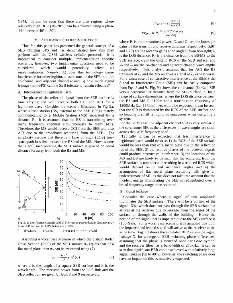
The phase of the reflected signal from the SEB surface is time varying and will produce both CCI and ACI for a legitimate user. Consider the scenario illustrated in Fig 9a, where a base station (BS) external to the SEB is legitimately communicating to a Mobile Station (MS) separated by a distance R. It is assumed that the BS is transmitting over many frequency channels simultaneously to many MSs. Therefore, the MS would receive CCI from the SEB and also ACI due to the broadband scattering from the SEB. For simplicity assume that there is a Line of Sight (LOS) free-space path loss link between the BS and the MS. Now assume that a wall incorporating the SEB surface is spaced an equal distance R1 away from both the BS and MS.
Fig. 9. a) Interference scenario and b) SIR versus perpendicular distance away from SEB surface, h. LOS distance R = 100m
[––– d=0.15m, ----- d=0.5m, – – – – d=1m and – – – d=2m]
Assuming a worst case scenario in which the bistatic Radar
Cross Section (RCS) of the SEB surface b equals that of a flat metal plate, then b can be estimated using (7). 購長 噺 替訂鳥填碇鉄 嫌件券態岫肯岻 (7)
where d is the length of a square SEB surface and is the wavelength. The received power from the LOS link and the SEB reflection are given by Eqs. 8 and 9 respectively.
鶏堅挑潮聴 噺 鶏痛 弔痛弔追碇轍鉄岫替訂眺岻鉄 (8) 鶏堅聴帳喋 噺 鶏痛 弔痛岫提岻弔追岫提岻蹄弐碇轍碇迭岫替訂岻典眺迭填 (9)
where Pt is the transmitted power, Gt and Gr are the boresight gains of the transmit and receive antennas respectively; Gt() and Gr() are the antenna gains at an angle from boresight; R is the LOS distance; R1 is the distance from the BS/MS to the SEB surface; b is the bistatic RCS of the SEB surface, and and are the co-channel and adjacent channel wavelengths respectively. This analysis assumes that for ACI the BS transmits at 1 and the MS receives a signal at 0 or visa versa. For a worst case of constructive interference at the BS/MS the Signal to Interference Ratio (SIR) can be easily computed from Eqs. 8 and 9. Fig. 9b shows the co-channel ( SIR versus perpendicular distance from the SEB surface, h, for a range of surface dimensions, where the LOS distance between the BS and MS R =100m for a transmission frequency of 1800MHz (0=167mm). As would be expected, it can be seen that the SIR is dominated by the RCS of the SEB surface and so keeping d small is highly advantageous when designing a system. For the GSM case, the adjacent channel SIR is very similar to the co-channel SIR as the differences in wavelengths are small across the GSM frequency band. Typically it can be expected that less interference to legitimate users would occur as 1) the RCS of the SEB surface would be less than that of a metal plate due to the reflection los of the SEB, 2) the relative phases of the received signals could produce destructive interference, 3) the locations of the MS and BS are likely to be such that the scattering from the SEB surface is non-specular resulting in a reduced RCS which would depend on d and incidence angles and 4) the assumption of flat metal plate scattering will give an underestimate of SIR as this does not take into account that the incident energy illuminating the SEB is redistributed over a broad frequency range once scattered.
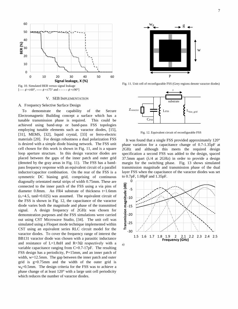
B. Signal leakage
Consider the case where a signal of unit amplitude illuminates the SEB surface. There will be a portion of the signal, X%, which does not pass through the SEB surface but arrives at the receiver due to leakage from the edges of the surface or through the walls of the building. Hence the portion of the signal that is impaired due to the SEB surface is (100-X)%. For a worst case scenario it is assumed that both the impaired and leaked signal will arrive at the receiver at the same time. Fig. 10 shows the simulated BER versus the signal leakage X, for a range of SEB switching phase differences, assuming that the phase is switched once per GSM symbol and the receiver filter has a bandwidth of 270kHz. It can be seen that significant BER can be achieved with relatively large signal leakage (up to 40%), however, the switching phase does have an impact on this as intuitively expected.
0
10
20
30
40
50
60
70
80
0 20 40 60 80 100
SIR
(d
B)
h (m)a) b)
MS
BS
R
h
d
R1
R1
7
Fig. 10. Simulated BER versus signal leakage [––– =60°, ----- =75° and – – – – =90°]
V. SEB IMPLEMENTATION
A. Frequency Selective Surface Design
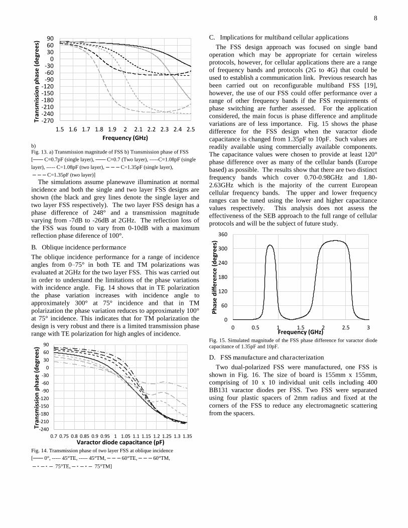
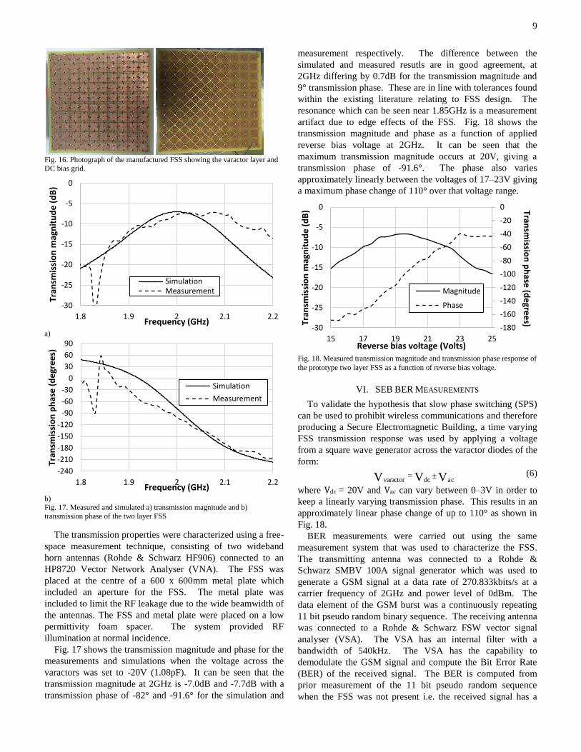
To demonstrate the capability of the Secure Electromagnetic Building concept a surface which has a tunable transmission phase is required. This could be achieved using band-stop or band-pass FSS topologies employing tunable elements such as varactor diodes, [15], [31], MEMS, [32], liquid crystal, [33] or ferro-electric materials [20]. For design robustness a dual polarization FSS is desired with a simple diode biasing network. The FSS unit cell chosen for this work is shown in Fig. 11, and is a square loop aperture structure. In this design varactor diodes are placed between the gaps of the inner patch and outer grid (denoted by the gray areas in Fig. 11). The FSS has a band-pass frequency response with an equivalent circuit of a parallel inductor/capacitor combination. On the rear of the FSS is a symmetric DC biasing grid, comprising of continuous diagonally orientated metal strips of width 0.75mm. These are connected to the inner patch of the FSS using a via pins of diameter 0.8mm. An FR4 substrate of thickness t=1.6mm (r=4.5, tan=0.025) was assumed. The equivalent circuit of the FSS is shown in Fig. 12, the capacitance of the varactor diode varies both the magnitude and phase of the transmitted signal. A design frequency of 2GHz was chosen for demonstration purposes and the FSS simulations were carried out using CST Microwave Studio, [34]. The unit cell was simulated using a Floquet mode technique implemented within CST using an equivalent series RLC circuit model for the varactor diodes. To cover the frequency range of interest the BB131 varactor diode was chosen with a parasitic inductance and resistance of L=1.8nH and R=3Ω respectively with a variable capacitance ranging from C=0.7-17pF. The resulting FSS design has a periodicity, P=15mm, and an inner patch of width, w=12.5mm. The gap between the inner patch and outer grid is g=0.75mm and the width of the outer grid is wg=0.5mm. The design criteria for the FSS was to achieve a phase change of at least 120° with a large unit cell periodicity which reduces the number of varactor diodes.
Fig. 11. Unit cell of reconfigurable FSS (Grey regions denote varactor diodes)
Fig. 12. Equivalent circuit of reconfigurable FSS
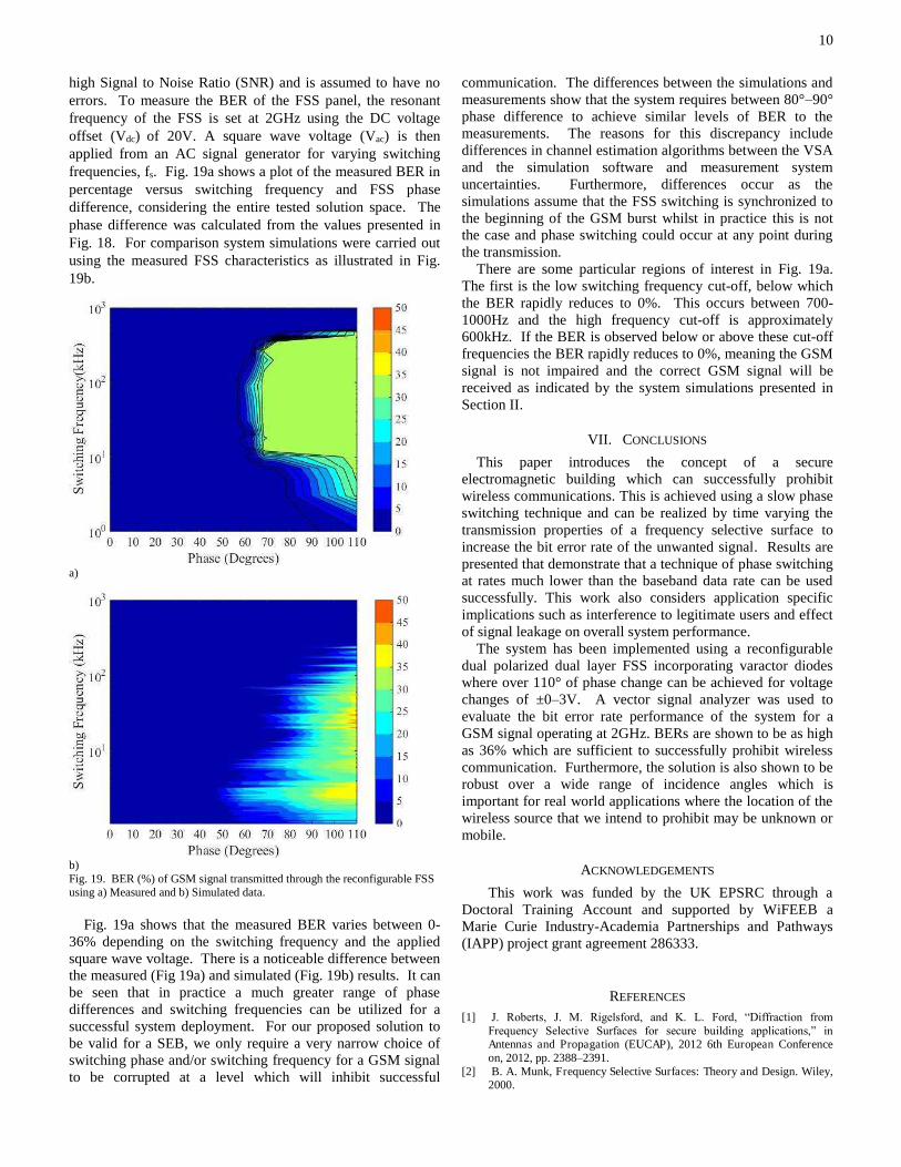
It was found that a single FSS provided approximately 120°
phase variation for a capacitance change of 0.7-1.35pF at 2GHz and although this meets the required design specification a second FSS was added to the design, spaced 37.5mm apart (/4 at 2GHz) in order to provide a design margin for the switching phase. Fig. 13 shows simulated transmission magnitude and transmission phase of the dual layer FSS when the capacitance of the varactor diodes was set to 0.7pF, 1.08pF and 1.35pF.
a)
0
10
20
30
40
50
60
0 10 20 30 40 50 60
BE
R (
%)
Signal leakage, X (%)
-30
-25
-20
-15
-10
-5
0
1.5 1.6 1.7 1.8 1.9 2 2.1 2.2 2.3 2.4 2.5
Tra
nsm
issi
on
ma
gn
itu
de
(d
B)
Frequency (GHz)
P
wg g
w
LFSS
CFSS
Zvaractor
substrate
Lbias_grid
t
8
b) Fig. 13. a) Transmission magnitude of FSS b) Transmission phase of FSS
[––– C=0.7pF (single layer), ––– C=0.7 (Two layer), -----C=1.08pF (single
layer), ----- C=1.08pF (two layer), – – – C=1.35pF (single layer),
– – – C=1.35pF (two layer)]
The simulations assume planewave illumination at normal incidence and both the single and two layer FSS designs are shown (the black and grey lines denote the single layer and two layer FSS respectively). The two layer FSS design has a phase difference of 248° and a transmission magnitude varying from -7dB to -26dB at 2GHz. The reflection loss of the FSS was found to vary from 0-10dB with a maximum reflection phase diference of 100°.
B. Oblique incidence performance
The oblique incidence performance for a range of incidence angles from 0–75° in both TE and TM polarizations was evaluated at 2GHz for the two layer FSS. This was carried out in order to understand the limitations of the phase variations with incidence angle. Fig. 14 shows that in TE polarization the phase variation increases with incidence angle to approximately 300° at 75° incidence and that in TM polarization the phase variation reduces to approximately 100° at 75° incidence. This indicates that for TM polarization the design is very robust and there is a limited transmission phase range with TE polarization for high angles of incidence.
Fig. 14. Transmission phase of two layer FSS at oblique incidence
[––– 0°, ----- 45°TE, ----- 45°TM, – – – 60°TE, – – – 60°TM,
– – – 75°TE, – – – 75°TM]
C. Implications for multiband cellular applications
The FSS design approach was focused on single band operation which may be appropriate for certain wireless protocols, however, for cellular applications there are a range of frequency bands and protocols (2G to 4G) that could be used to establish a communication link. Previous research has been carried out on reconfigurable multiband FSS [19], however, the use of our FSS could offer performance over a range of other frequency bands if the FSS requirements of phase switching are further assessed. For the application considered, the main focus is phase difference and amplitude variations are of less importance. Fig. 15 shows the phase difference for the FSS design when the varactor diode capacitance is changed from 1.35pF to 10pF. Such values are readily available using commercially available components. The capacitance values were chosen to provide at least 120° phase difference over as many of the cellular bands (Europe based) as possible. The results show that there are two distinct frequency bands which cover 0.70-0.98GHz and 1.80-2.63GHz which is the majority of the current European cellular frequency bands. The upper and lower frequency ranges can be tuned using the lower and higher capacitance values respectively. This analysis does not assess the effectiveness of the SEB approach to the full range of cellular protocols and will be the subject of future study.
Fig. 15. Simulated magnitude of the FSS phase difference for varactor diode capacitance of 1.35pF and 10pF.
D. FSS manufacture and characterization
Two dual-polarized FSS were manufactured, one FSS is shown in Fig. 16. The size of board is 155mm x 155mm, comprising of 10 x 10 individual unit cells including 400 BB131 varactor diodes per FSS. Two FSS were separated using four plastic spacers of 2mm radius and fixed at the corners of the FSS to reduce any electromagnetic scattering from the spacers.
-270-240-210-180-150-120
-90-60-30
0306090
1.5 1.6 1.7 1.8 1.9 2 2.1 2.2 2.3 2.4 2.5
Tra
nsm
issi
on
ph
ase
(d
eg
ree
s)
Frequency (GHz)
-240
-210
-180
-150
-120
-90
-60
-30
0
30
60
90
0.7 0.75 0.8 0.85 0.9 0.95 1 1.05 1.1 1.15 1.2 1.25 1.3 1.35
Tra
nsm
issi
on
ph
ase
(d
eg
ree
s)
Varactor diode capacitance (pF)
0
60
120
180
240
300
360
0 0.5 1 1.5 2 2.5 3
Ph
ase
dif
fere
nce
(d
eg
ree
s)
Frequency (GHz)
9
Fig. 16. Photograph of the manufactured FSS showing the varactor layer and DC bias grid.
a)
b) Fig. 17. Measured and simulated a) transmission magnitude and b) transmission phase of the two layer FSS
The transmission properties were characterized using a free-
space measurement technique, consisting of two wideband horn antennas (Rohde & Schwarz HF906) connected to an HP8720 Vector Network Analyser (VNA). The FSS was placed at the centre of a 600 x 600mm metal plate which included an aperture for the FSS. The metal plate was included to limit the RF leakage due to the wide beamwidth of the antennas. The FSS and metal plate were placed on a low permittivity foam spacer. The system provided RF illumination at normal incidence.
Fig. 17 shows the transmission magnitude and phase for the measurements and simulations when the voltage across the varactors was set to -20V (1.08pF). It can be seen that the transmission magnitude at 2GHz is -7.0dB and -7.7dB with a transmission phase of -82° and -91.6° for the simulation and
measurement respectively. The difference between the simulated and measured resutls are in good agreement, at 2GHz differing by 0.7dB for the transmission magnitude and 9° transmission phase. These are in line with tolerances found within the existing literature relating to FSS design. The resonance which can be seen near 1.85GHz is a measurement artifact due to edge effects of the FSS. Fig. 18 shows the transmission magnitude and phase as a function of applied reverse bias voltage at 2GHz. It can be seen that the maximum transmission magnitude occurs at 20V, giving a transmission phase of -91.6°. The phase also varies approximately linearly between the voltages of 17–23V giving a maximum phase change of 110° over that voltage range.
Fig. 18. Measured transmission magnitude and transmission phase response of the prototype two layer FSS as a function of reverse bias voltage.
VI. SEB BER MEASUREMENTS
To validate the hypothesis that slow phase switching (SPS) can be used to prohibit wireless communications and therefore producing a Secure Electromagnetic Building, a time varying FSS transmission response was used by applying a voltage from a square wave generator across the varactor diodes of the form:
VVV ±= dcvaractor ac (6)
where Vdc = 20V and Vac can vary between 0–3V in order to keep a linearly varying transmission phase. This results in an approximately linear phase change of up to 110° as shown in Fig. 18.
BER measurements were carried out using the same measurement system that was used to characterize the FSS. The transmitting antenna was connected to a Rohde & Schwarz SMBV 100A signal generator which was used to generate a GSM signal at a data rate of 270.833kbits/s at a carrier frequency of 2GHz and power level of 0dBm. The data element of the GSM burst was a continuously repeating 11 bit pseudo random binary sequence. The receiving antenna was connected to a Rohde & Schwarz FSW vector signal analyser (VSA). The VSA has an internal filter with a bandwidth of 540kHz. The VSA has the capability to demodulate the GSM signal and compute the Bit Error Rate (BER) of the received signal. The BER is computed from prior measurement of the 11 bit pseudo random sequence when the FSS was not present i.e. the received signal has a
-30
-25
-20
-15
-10
-5
0
1.8 1.9 2 2.1 2.2
Tra
nsm
issi
on
ma
gn
itu
de
(d
B)
Frequency (GHz)
Simulation
Measurement
-240
-210
-180
-150
-120
-90
-60
-30
0
30
60
90
1.8 1.9 2 2.1 2.2
Tra
nsm
issi
on
ph
ase
(d
eg
ree
s)
Frequency (GHz)
Simulation
Measurement
-180
-160
-140
-120
-100
-80
-60
-40
-20
0
-30
-25
-20
-15
-10
-5
0
15 17 19 21 23 25
Tra
nsm
ission
ph
ase
(de
gre
es)T
ran
smis
sio
n m
ag
nit
ud
e (
dB
)
Reverse bias voltage (Volts)
Magnitude
Phase
10
high Signal to Noise Ratio (SNR) and is assumed to have no errors. To measure the BER of the FSS panel, the resonant frequency of the FSS is set at 2GHz using the DC voltage offset (Vdc) of 20V. A square wave voltage (Vac) is then applied from an AC signal generator for varying switching frequencies, fs. Fig. 19a shows a plot of the measured BER in percentage versus switching frequency and FSS phase difference, considering the entire tested solution space. The phase difference was calculated from the values presented in Fig. 18. For comparison system simulations were carried out using the measured FSS characteristics as illustrated in Fig. 19b.
a)
b) Fig. 19. BER (%) of GSM signal transmitted through the reconfigurable FSS using a) Measured and b) Simulated data.
Fig. 19a shows that the measured BER varies between 0-36% depending on the switching frequency and the applied square wave voltage. There is a noticeable difference between the measured (Fig 19a) and simulated (Fig. 19b) results. It can be seen that in practice a much greater range of phase differences and switching frequencies can be utilized for a successful system deployment. For our proposed solution to be valid for a SEB, we only require a very narrow choice of switching phase and/or switching frequency for a GSM signal to be corrupted at a level which will inhibit successful
communication. The differences between the simulations and measurements show that the system requires between 80°–90° phase difference to achieve similar levels of BER to the measurements. The reasons for this discrepancy include differences in channel estimation algorithms between the VSA and the simulation software and measurement system uncertainties. Furthermore, differences occur as the simulations assume that the FSS switching is synchronized to the beginning of the GSM burst whilst in practice this is not the case and phase switching could occur at any point during the transmission.
There are some particular regions of interest in Fig. 19a. The first is the low switching frequency cut-off, below which the BER rapidly reduces to 0%. This occurs between 700-1000Hz and the high frequency cut-off is approximately 600kHz. If the BER is observed below or above these cut-off frequencies the BER rapidly reduces to 0%, meaning the GSM signal is not impaired and the correct GSM signal will be received as indicated by the system simulations presented in Section II.
VII. CONCLUSIONS
This paper introduces the concept of a secure electromagnetic building which can successfully prohibit wireless communications. This is achieved using a slow phase switching technique and can be realized by time varying the transmission properties of a frequency selective surface to increase the bit error rate of the unwanted signal. Results are presented that demonstrate that a technique of phase switching at rates much lower than the baseband data rate can be used successfully. This work also considers application specific implications such as interference to legitimate users and effect of signal leakage on overall system performance.
The system has been implemented using a reconfigurable dual polarized dual layer FSS incorporating varactor diodes where over 110° of phase change can be achieved for voltage changes of ±0–3V. A vector signal analyzer was used to evaluate the bit error rate performance of the system for a GSM signal operating at 2GHz. BERs are shown to be as high as 36% which are sufficient to successfully prohibit wireless communication. Furthermore, the solution is also shown to be robust over a wide range of incidence angles which is important for real world applications where the location of the wireless source that we intend to prohibit may be unknown or mobile.
ACKNOWLEDGEMENTS
This work was funded by the UK EPSRC through a Doctoral Training Account and supported by WiFEEB a Marie Curie Industry-Academia Partnerships and Pathways (IAPP) project grant agreement 286333.
REFERENCES [1] J. Roberts, J. M. Rigelsford, and K. L. Ford, “Diffraction from
Frequency Selective Surfaces for secure building applications,” in Antennas and Propagation (EUCAP), 2012 6th European Conference on, 2012, pp. 2388–2391.
[2] B. A. Munk, Frequency Selective Surfaces: Theory and Design. Wiley, 2000.
11
[3] J. C. Batchelor, E. A. Parker, B. Sanz-Izquierdo, J. B. Robertson, I. T. Ekpo, and A. G. Williamson, “Designing FSS for wireless propagation control within buildings,” in Loughborough Antennas and Propagation Conference, LAPC 2009 - Conference Proceedings, 2009, pp. 14–17.
[4] G. H. H. Sung, K. W. Sowerby, M. J. Neve, and A. G. Williamson, “A frequency-selective wall for interference reduction in wireless indoor environments,” IEEE Antennas Propag. Mag., vol. 48, pp. 29–37, 2006.
[5] M. Raspopoulos and S. Stavrou, “Frequency Selective Buildings Through Frequency Selective Surfaces,” IEEE Trans. Antennas Propag., vol. 59, pp. 2998–3005, 2011.
[6] M. Y. M. Yang and A. Brown, “Simulation of propagation through a frequency selective wall at 3 GHz,” Antennas Propag. (EuCAP), 2010 Proc. Fourth Eur. Conf., 2010.
[7] M. Yang and A. K. Brown, “A hybrid model for radio wave propagation through frequency selective structures (FSS),” IEEE Trans. Antennas Propag., vol. 58, pp. 2961–2968, 2010.
[8] Y.-M. Yu, C.-N. Chiu, Y.-P. Chiou, and T.-L. Wu, “A Novel 2.5-Dimensional Ultraminiaturized-Element Frequency Selective Surface,” IEEE Trans. Antennas Propag., vol. 62, no. 7, pp. 3657–3663, Jul. 2014.
[9] M. Gustafsson, A. Karlsson, A. P. P. Rebelo, and B. Widenberg, “Design of frequency selective windows for improved indoor outdoor communication,” IEEE Trans. Antennas Propag., vol. 54, pp. 1897–1900, 2006.
[10] G. I. Kiani, A. R. Weily, and K. P. Esselle, “A novel absorb/transmit FSS for secure indoor wireless networks with reduced multipath fading,” IEEE Microw. Wirel. Components Lett., vol. 16, pp. 378–380, 2006.
[11] F. Bayatpur and K. Sarabandi, “A tunable metamaterial frequency-selective surface with variable modes of operation,” IEEE Trans. Microw. Theory Tech., vol. 57, pp. 1433–1438, 2009.
[12] J. A. Bossard, X. Liang, L. Li, S. Yun, D. H. Werner, B. Weiner, T. S. Mayer, P. F. Cristman, A. Diaz, and I. C. Khoo, “Tunable frequency selective surfaces and negative-zero-positive index metamaterials based on liquid crystals,” IEEE Trans. Antennas Propag., vol. 56, pp. 1308–1320, 2008.
[13] W. Hu, R. Dickie, R. Cahill, H. Gamble, Y. Ismail, V. Fusco, D. Linton, N. Grant, and S. Rea, “Liquid crystal tunable mm wave frequency selective surface,” IEEE Microw. Wirel. Components Lett., vol. 17, pp. 667–669, 2007.
[14] G. I. Kiani, K. L. Ford, L. G. Olsson, K. P. Esselle, and C. J. Panagamuwa, “Switchable frequency selective surface for reconfigurable electromagnetic architecture of buildings,” IEEE Trans. Antennas Propag., vol. 58, pp. 581–584, 2010.
[15] C. Mias, “Varactor-tunable frequency selective surface with resistive-lumped-element biasing grids,” in IEEE Microwave and Wireless Components Letters, 2005, vol. 15, pp. 570–572.
[16] C. Mias and J. H. Yap, “A varactor-tunable high impedance surface with resistive-lumped-element biasing grid,” IEEE Trans. Antennas Propag., vol. 55, pp. 1955–1962, 2007.
[17] A. Munir, V. Fusco, and O. Malyuskin, “Tunable frequency selective surfaces characterisation,” in Proceedings of the 38th European Microwave Conference, EuMC 2008, 2008, pp. 813–816.
[18] B. Sanz-Izquierdo, E. A. Parker, and J. C. Batchelor, “Switchable frequency selective slot arrays,” IEEE Trans. Antennas Propag., vol. 59, pp. 2728–2731, 2011.
[19] B. Sanz-Izquierdo, E. A. Parker, and J. C. Batchelor, “Dual-band tunable screen using complementary split ring resonators,” IEEE Trans. Antennas Propag., vol. 58, pp. 3761–3765, 2010.
[20] M. Sazegar, Y. Zheng, C. Kohler, H. Maune, M. Nikfalazar, J. R. Binder, and R. Jakoby, “Beam steering transmitarray using tunable frequency selective surface with integrated ferroelectric varactors,” IEEE Trans. Antennas Propag., vol. 60, pp. 5690–5699, 2012.
[21] F. Bayatpur and K. Sarabandi, “Single-layer high-order miniaturized-element frequency-selective surfaces,” IEEE Trans. Microw. Theory Tech., vol. 56, pp. 774–781, 2008.
[22] H. Liu, K. L. Ford, and R. J. Langley, “Miniaturised bandpass frequency selective surface with lumped components,” Electronics Letters, vol. 44. p. 1054, 2008.
[23] H. L. Liu, K. L. Ford, and R. J. Langley, “Design methodology for a miniaturized frequency selective surface using lumped reactive components,” IEEE Trans. Antennas Propag., vol. 57, pp. 2732–2738, 2009.
[24] B. Sanz-Izquierdo, J. B. Robertson, E. A. Parker, and J. C. Batchelor, “Minimal size of operation of fractal FSS,” in IEEE Antennas and Propagation Society, AP-S International Symposium (Digest), 2009.
[25] O. Malyuskin and V. Fusco, “Spatial Data Encryption Using Phase Conjugating Lenses,” IEEE Trans. Antennas Propag., vol. 60, no. 6, pp. 2913–2920, Jun. 2012.
[26] K. L. Ford, G. Fong, J. Rigelsford, S. Zhou, and J. Roberts, “Reconfigurable frequency selective surface for use in secure electromagnetic buildings,” Electron. Lett., vol. 49, no. 14, pp. 861–863, Jul. 2013.
[27] B. Chambers and A. Tennant, “The phase-switched screen,” IEEE Antennas Propag. Mag., vol. 46, no. 6, pp. 23–37, 2004.
[28] Y. Ding and V. F. Fusco, “Establishing Metrics for Assessing the Performance of Directional Modulation Systems,” IEEE Trans. Antennas Propag., vol. 62, no. 5, pp. 2745–2755, May 2014.
[29] S. M. Redl, M. K. Weber, and M. W. Oliphant, An introduction to GSM. Artech House Publishers, 1995.
[30] H. Gunnar, GSM Networks: Protocols, Terminology and Implementation. Artech House Publishers, 1998.
[31] H. J. Lee, K. L. Ford, and R. J. Langley, “Independently Tunable Low-Profile Dual-Band High-Impedance Surface Antenna System for Applications in UHF Band,” IEEE Trans. Antennas Propag., vol. 60, no. 9, pp. 4092–4101, 2012.
[32] F. Surfaces, G. M. Coutts, R. R. Mansour, S. K. Chaudhuri, S. Member, and A. Abstract, “Microelectromechanical Systems Tunable Structures on Rigid-Flex Substrates,” IEEE Trans. Microw. THEORY Tech., vol. 56, no. 7, pp. 1737–1746, 2008.
[33] E. Doumanis, G. Goussetis, R. Dickie, R. Cahill, and P. Baine, “Electronically Recon fi gurable Liquid Crystal Based Mm-Wave Polarization Converter,” IEEE Trans. ANTENNAS PROPAGATION, vol. 62, no. 4, pp. 2302–2307, 2014.
[34] “CST Microwave Studio.” [Online]. Available: www.cst.com.
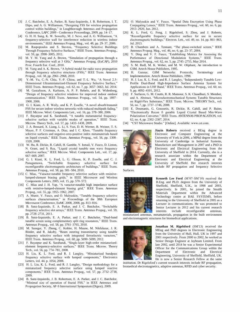
Jiayin Roberts received a BEng degree in Electronic and Computer Engineering at the University of York in 2006, a MPhil degree from the University of Cambridge in Industrial Systems, Manufacture and Management in 2007 and a PhD in Electronic and Electrical Engineering from the University of Sheffield in 2014. Currently, she is a research associate within the Department of Electronic and Electrical Engineering at the University of Sheffield. Her research interests include RF propagation and frequency Selective
Surfaces.
Kenneth Lee Ford (M’07–SM’10) received the B.Eng. and Ph.D. degrees from the University of Sheffield, Sheffield, U.K., in 1998 and 2003, respectively. In 2001, he joined the Stealth Materials Department within the Advanced Technology centre at BAE SYSTEMS, before returning to the University of Sheffield in 2005 as a Lecturer in communications. He was promoted to Senior Lecturer in 2012 and his current research interests include reconfigurable antennas,
miniaturized antennas, metamaterials, propagation in the built environment and electromagnetic structures for biomedical applications.
Jonathan M. Rigelsford (SM'13) received the MEng and PhD degrees in Electronic Engineering from the University of Hull, Hull, UK in 1997 and 2001 respectively. From 2000 to 2002, he worked as Senior Design Engineer at Jaybeam Limited. From late 2002, until 2014 he was a Senior Experimental Officer for the Communications Group within the Department of Electronic and Electrical Engineering, University of Sheffield, Sheffield, UK. He is now a Senior Research Fellow at the same
institution. Dr Rigelsford’s current research interests include RF propagation, biomedical electromagnetics, adaptive antennas, RFID and cyber security.