screen printing: a technology for the batch fabrication of
TRANSCRIPT
ELSEVIER Sensors and Actuators B 21 (1994) 171-183 CHEMICAL
Screen printing: a technology for the batch fabrication of integrated chemical-sensor arrays
Howard D. Goldberg”>*, Richard B. Browna, Dong P. Liub, Mark E. Meyerho@’ Wepanmenl of Electrical Engineering and Computer Science, Universiry of Michigan, Ann Ab, MI 48109, USA
%epariment of Chemkhy, Um’versi@ of Michigan, Ann Ark MI 48109, USA
Received 5 July 1993; in revised form 31 January 1994, accepted 8 February 1994
Abstract
The commercialization of integrated chemical sensors has been slowed by the difficulty of device encapsulation and membrane application. For reasons of both cost and reproducibility, the sensor-specific structures should be mass fabricated, as are the microelectronics. The challenge lies in merging the standard semiconductor process sequence with the non-standard steps used to form the transducers. We demonstrate that screen printing can be used to partition the fabrication into two distinct sequences, semiconductor processing and sensor-specific steps. This simplifies process development and evolution, and makes semiconductor foundry services available for manufacturing sensors. After conventional semiconductor processing, our wafers have silver epoxy contacts screen printed on the aluminum sensor pads; the silver forms a stable chemical interface to the membranes, and the epoxy makes a strong physical bond to them. Next, the polymeric membranes are applied and patterned with screen printing. Membranes of different compositions can be deposited on the various sites of a multisensor chip by simply repeating the screen print/cure cycle. We show that the electrochemical performance of mass-fabricated passive and active sensor arrays is comparable to that of conventional liquid-junction ion-selective electrodes.
K~ords: Batch fabrication; Chemical sensor arrays; Screen printing
1. Introduction
To succeed in the marketplace, integrated sensors must fill application needs reliably and cost effectively. The deposition of sensor-specific layers must be done cast effectively and reproducibly. To satisfy many present and future applications, chemical sensors should include integrated circuitry. This requires the deposition of the sensor-specific layers and the encapsulation of the de- vices to be compatible with mass fabrication and stan- dard CMOS processing. A fabrication approach that decouples the semiconductor process sequence from the non-standard steps used to form the transducer(s) allows independent optimization of the processes [l]. The concept of process partitioning has been dem- onstrated in sensors where micromachined structures are merged with interface electronics [2].
The most common method for applying polymeric membranes to solid-state sensors has been solvent cast- ing, which requires hand work under a microscope [3,4].
*Author to whom correspondence should be addressed at the Microsystems Technology Laboratories, Massachusetts Institute of Technology, Bldg. 39-561, Cambridge, MA 02139, USA.
Given the small size of the sensors, this is a tedious task, and the source of greatest yield loss. Control of membrane thickness and shape is difficult, resulting in a lack of sensor reproducibility. Others have also ad- dressed the problem of membrane application. A tech- nique that involves conformally coating the chip with a blank membrane and selectively doping the membrane over the sensing sites has been reported [5]. This method requires large chip geometries to avoid electrode cross- talk in multisensing devices, and suffers from lateral diffusion of the ionophore over time. A photoresist lift- off method has resulted in precisely patterned mem- branes [6], but this technique exposes the membranes to organic lift-off solvents, which may alter their elec- trochemical characteristics, and the range of thicknesses is limited to those that can be realized in photoresist. Photolithographically pattemable membranes have been reported [7], but they have poor adhesion to the metal electrodes and require comparatively large spaces be- tween sensor sites. In a sensor array, this approach would expose membranes to cross-contamination as successive layers are applied. Computer-controlled sy- ringe dispensing systems have been developed to deposit
Elsevier Science S.A. SSDI 0925-4005(94)01249-H

172 H.D. Goldberg et al. / Sensors and Achutom B 21 (1994) 171-183
various sensor layers across a wafer [8,9]; the expected throughput rate is low, especially for wafers containing sensor arrays, and the resulting membranes are usually thin (i.e., 20 pm [S]), which shortens sensor lifetimes due to ionophore leaching.
To apply the sensor-specific layers reliably and cost effectively, we have employed screen printing. Initial results in patterning silver epoxy electrode contacts and polymeric membranes demonstrated the feasibility of this approach [lo]. Our work benefitted from devel- opments in the screen printing of polymers for pas- sivation of electronic circuits [ll]. Screen printing de- posits the contacts or membranes on a full wafer at a time. It can form thick layers, has short cycle times, is reproducible, allows precise pattern control, and is additive (no waste of material). To make this method feasible, the membranes, which had already been op- timized for electrochemical and adhesive properties [12-141, had to be optimized for screen printability. To be specific, we needed to modify the membrane paste in order to minimize lateral flow-out and yield thicker membranes. Based on this effort, an initial set of screen-printing parameters and limitations was pre- sented for passive solid-state chemical sensor fabrication [15,16].
Others have reported the use of screen printing to deposit glass-based pastes for hybrid pH sensors [17-191 and to deposit conductive pastes to form the electrode layers for various hybrid chemical sensors [20-221. These materials require firing temperatures above 800 “C to cure the deposited materials, so they cannot be inte- grated with CMOS circuitry - one of our goals for improving the manufacturability of chemical sensors.
This use of screen printing in the fabrication of chemical sensors has enabled the microsensor manu- facturing sequence to be easily partitioned, as shown in Fig. 1. Conventional CMOS processing is used to form the on-chip electronics, after which overglass openings are made to the aluminum sensor pads at the same time as the bonding-pad regions are opened; screen printing is then used to deposit the sensor- specific layers. Screen printing adds rheological con- straints to materials [23,24], but it eliminates the need for developing, etching, and lift-off, processing steps that are more complicated and might alter the elec- trochemical characteristics of the sensing layers. Fur- thermore, the materials involved can be applied and cured at relatively low temperatures, so that the sensor- specific steps can be done after CMOS processing. Recently, others have also used screen printing to form chemical transducers [25]; their relatively simple sensors were formed on large ceramic substrates.
To demonstrate the benefits of this new manufacturing technology, several types of sensor chips of varying complexity were designed and fabricated.
Microelectronic
a
Probe Electronics for Functionality
a Screen Print Single
Sensor-Specific Layer I?
Sensor-Specific
Cut Wafer Into Die, Wirebond, and Package
V Test Complete Sensor
for Functionality I
Fig. 1. Partitioned process flow for mass-fabricated sensor arrays.
Silicon Nitride Polymer Membrane
I
Silicon Substrate T + Silicon Dioxide
Fig. 2. Cross-sectional view of a solid-state microelectrode.
(1) The first of these were miniature, multi-site, ion- selective electrodes (ISEs) (the sensor cross section is shown in Fig. 2). Several clinical and environmental monitoring applications would benefit from the avail- ability of low-cost/disposable passive chemical sensors like these that could be used with portable instru- mentation.
(2) The second sensor type was a multisensor chip with four buffered ion-selective electrodes; a floorplan of this design is shown in Fig. 3. A control line switches the input between the transducer and system ground, allowing periodic calibration of the circuit offset po- tentials by the host controller. Such sensors are well

H.D. Goldbeg et al. I Sensors and Achumm B 21 (1994) 171-183 173
Ion-Srbctive El&rode Sits
k.
Ground-
Signal Buffering
Fig. 3. Floorplan of the basic chemical multisensor chip.
suited to applications in industrial process control, the manufacture of foodstuffs, and the pharmaceutical in- dustry, for example, which need remote sensors that can be readily configured by a control system (i.e., microcomputer or microcontroller) and can reliably communicate sensor data back to the host controller. The remote sensor effectively closes the system control loop, allowing the host controller to make real-time decisions that result in the initiation of actuator-driven control sequences.
(3) The third type of sensor is represented by Fig. 4. This programmable multisensor chip offers 14 user- programmable readout modes, a programmable gain stage, a 1Zbit analog-to-digital converter, and an RS- 422 serial communication interface. This stand-alone multisensor chip includes a temperature sensor and four buffered ion-selective electrode sites with switching circuitry at the inputs, which allow system ground or a reference voltage to be read. The sensor allows calibration for the temperature sensitivity of the elec- trochemical responses, and circuit offset and gain drift with time and temperature. This more complicated device can be configured for use in a wide range of applications.
Affordable sensor arrays such as these can provide multicomponent analysis, interference compensation, redundancy, and extended dynamic range.
There have been several reported attempts to fab- ricate the reference electrode on-chip with the sensing element; some of these efforts have included the de- position of silver/silver chloride films, the utilization of ISFETs/ISEs coated with hydrophobic ion-blocking
Grand (Rsfamnce Ebctroda)
Switch Control
polymer membranes [26], and the micromachining of liquid-junction reference electrodes [27,28]. Typically, microfabricated reference electrodes require specific operating conditions (i.e., constant chloride activity or pH range), exhibit significant drift of the reference potential, and/or have reproducibility problems. The nature of each individual sensing application determines the type of reference electrode that is required. Con- tinuous on-line integrated sensors require the electro- chemical stability of a conventional liquid-junction reference electrode. For most applications, the mini- aturization of this reference electrode would be the most cost-effective approach for overall compatibility with planar mass-fabricated chemical sensors. This can be realized with either f&tipped catheters with an internal wire and filling solution or injection-molded integrated sensor packages containing a liquid-filled chamber and plastic frit. Reference electrodes with short-term stability can be used with sensors in flow- injection systems, because such systems calibrate for the baseline drift of the electrochemical cell. Mass- fabricated chemical sensor arrays could also be con- sidered as low-cost/replaceable parts to be plugged into portable instrumentation, which would already contain a high-quality reference electrode.
2. Polymeric membrane characterization
The two membrane pastes we characterized for screen printing are a polyurethane-based matrix PUI(PVcIAc/ Al), which had been previously optimized for adhesion and electrochemical performance, and a moisture-cu-

174 H.D. Goldberg et al. I Sensors and Achrators B 21 (1994) 171483
Fig. 4. Floorplan of the programmable chemical multisensor chip.
rable silicone rubber matrix, which also exhibits excellent adhesion and electrochemical characteristics. The prep- aration and electrochemical performance of the PU/ (PVC/AC/AI) membrane (matrix composition: PU 26.4 wt.%, 6.6 wt.% copolymer of vinyl chloride/vinyl acetate/ vinyl alcohol (PVC/Ac/A.l: 85/5/15 wt.%), 66 wt.% plas- ticizer, and 1 wt.% neutral carrier) have been previously reported by our research group [14]. The silicone rubber matrix is composed of 97.2 wt.% silicone rubber (RTV 3140; Dow Corning), 1 wt.% potassium tetrakis(p- chlorophenyl)borate, and 1.8 wt.% ionophore. This silicone rubber matrix offers lower membrane resistance than the Petrarch silicone rubber-based membrane ma- trix previously reported by our group [14]. Fig. 5 shows the structure of the polymer matrices used to prepare the ion-selective membrane pastes for the integrated chemical sensors.
The screen-printing process is illustrated in Fig. 6. Masks are composed of either a stainless-steel mesh coated with a photoreactive emulsion, or a metal-foil stencil. The screen printer applies the membrane paste evenly to the mask and rubs it with a squeegee, which pushes the paste through the openings in the mask onto the substrate. Solvents are used to achieve mem- brane paste with appropriate viscosity (for resistance to flow from squeegee motion) and thixotropy (for resistance to secondary flow after the mask is removed from the substrate) for good pattern definition. The membrane/solvent system plays a significant role in determining the screenability of the resulting paste. Anhydrous tetrahydrofuran (THF), which is commonly used to solvent-cast membranes, is unacceptable in a screen-printing membrane paste because its high solvent
Cl H H H Cl H H
I I I I I I I -c-c-c-c-c-c-c-
l I I I I I I H H 0 H H II OH
I c=o
CH,-&-CH,
CH, :, I
Cn,
-~-Si--iF_~i-~-~i-0_ I
c, y
CH,- Si-CH,
I ?
Fig. 5. Structure of the polymer matrices used for preparing ion-
selective membrane pastes for the potentiometric chemical sensors: A, vinyl chloride/vinyl acetate/vinyl alcohol copolymer (PVC/AC/AI);
B, Tecoflex polyurethane; C, Dow Coming RTV 3140 silicone rubber.

H.D. Goldberg et al. / Sen.wrs and Actuators B 21 (1994) 171-183 175
Fig. 6. The screen-printing process.
evaporation rate causes the viscosity of the paste to change rapidly, and it soon clogs the mask.
The use of higher boiling-point (i.e., lower evaporation rates) solvents such as N,N-dimethylacetamide (DMA) and cyclohexanone was investigated. Pastes composed of the PLJ/(PVC/Ac/Al) matrix dissolved in various combinations of DMARHF and cyclohexanoneRI-IF solvents were screen printed. The THF was used to dissolve the membrane components, after which it was evaporated from the final paste solution in a vacuum desiccator. Though viscosity was controlled with this mixture [lo], the membrane pastes needed to be further optimized to reduce the flow-out of the printed mem- branes. As a result, 1-methyl-2-pyrrolidinone was in- vestigated as a potential solvent system for the PU/ (PVC/AC/AI) membrane paste. As before, THF was added to the initial membrane solution and was later evaporated from the final membrane paste. Pastes with good viscosity and thixotropy were achieved with this solvent system. Though the higher boiling-point solvent resulted in a paste with good screenability, when silicon tetrachloride was added to the paste to increase mem- brane adhesion and improve the resulting electrode stability, the paste began to gel on the mask, probably because the SiCl, initiated cross-linking of the matrix.
Inert fillers such as silica powder are often employed to improve the rheology of screen-printing pastes [29,30]. Fumed silica powder (particle size 0.007 pm; Sigma Chemical Co.) was added to the polyurethane-based membrane to improve its pattern definition. Because a large percentage of silica powder had to be added to achieve the desiredviscosity, the resulting membranes had numerous pinholes and irregularities.
In another effort, the total amount of solvent was reduced in order to increase the paste viscosity and thixotropy: this was expected to yield thicker membranes with reduced lateral flowout. As the solvent amount was decreased, the paste became tacky and stringy and began to gel on the mask, making screen printing difficult. The screen-printing process increases the sol- vent evaporation rate as it spreads a thin layer of the paste onto the screen mask, increasing the amount of surface area of the membrane paste exposed to the air. This effect sets a bound on how much solvent had to be used in the paste; the resulting membranes were
thinner and had poorer pattern definition than was acceptable.
Good screen-printing results were finally achieved by using PI-Thinner (Epoxy Technology), a proprietary mixture of various high boiling-point solvents, in the membrane paste. The PU/(PVC/Ac/Al) components (66 mg of polymeric material) are first completely dissolved in 1.2 ml of THF, after which 0.1 ml of PI-Thinner is added and mixed thoroughly. The low boiling-point THF is evaporated from the resulting membrane paste and 7 wt.% of Sic& is added just prior to screen printing. The past exhibits good screenability, membrane thickness, and pattern definition. The cure cycle consists of a 1 h convection oven bake at 70 “C to accelerate the PI-Thinner evaporation process, followed by a room- temperature cure for 24 h.
In contrast to the polyurethane-based membranes, silicone rubber membrane pastes are easier to prepare for screen printing. The silicone rubber membrane components are first completely dissolved in 1.2 ml of THF. The THF is evaporated and the resulting paste is ready for screen printing. No Sic& is added to this matrix, since the membrane adhesion is excellent and the adhesion promoter significantly reduces the elec- trochemical response of these membranes. This re- duction in electrochemical response may be the result of increased membrane self-adhesion (hindering the ion-exchange process); the silicone rubber contains trimethylated silica and hydroxyl-terminated polydi- methylsiloxane (refer to Fig. 5C), which may react with SiCl,. The silicone rubber paste exhibits better viscosity and thixotropy than the PU/(PVC/Ac/Al) paste. The silicone rubber membranes are cured at room tem- perature for 24 h to allow the vulcanizing process to occur.
3. Screen-printing parameters
Stainless-steel stencil masks (Micro-Screen, Inc.) were chosen to print the silver epoxy electrode contact (H20E; Epoxy Technology) and the polymer membranes on the solid-state sensors. The stencil masks offer longer lifetimes and better solvent resistance than emulsion masks. The thickness of pre-cured patterned layers is ideally determined by the mask thickness, which can be specified over a 25-250 pm range. Screens and printing equipment now available allow alignment and reproducibility to f5 pm. Tbe screen printer used in this work is semi-automated and optically aligned (LS- 15TV; New Long Co.). The throughput rate (set-up, test print for alignment purposes, alignment, and print) is approximately 5 min per wafer; this is independent of the number of sensor die on the wafer.
The print quality of the deposited material is a function of mask clearance from the substrate, squeegee

176
Table 1 Screen-printing parameters
H.D. GoldbeT et al. I Sensors and Achrators B 21 (1994) 171-183
Parameter Silver epoxy PU/(PVC/Ac/Al) Silicone rubber
Mask clearance (mm) 0 Squeegee shape diamond
Squeegee Speed (mm/s) 100 Squeegee pressure (k@n?) 0.9 Squeegee angle none Push-in quantity (mm) 0.1
speed, squeegee shape, squeegee angle, squeegee pres- sure, and squeegee push-in quantity. We have found that the edge quality of the pattern is influenced most by the squeegee shape and mask clearance from the substrate. Pattern flow-out and thickness are determined primarily by squeegee speed, pressure, and push-in quantity. If the squeegee speed is too fast or there is not enough pressure or push-in quantity, the pattern may not be completely filled by the paste, and the deposited material may form peaks instead of having a smooth profile. If the speed is too slow and the pressure or push-in quantity is too great, the flow-out will increase and the pattern thickness may decrease due to the ‘scavenging’ effects of the squeegee.
Even though silver epoxy is commercially available as a screen-printable paste, the silver epoxy printing parameters had to be carefully optimized, along with those for the polymeric membranes. Table 1 lists the optimized screen-printing parameters used to print the various sensor layers. The silver epoxy was cured for 15 min iu a 150 “C oven. These parameters have to be adjusted slightly from run to run to account for slight variations in the rheology of the membrane paste.
The pattern-definition quality of the respective sensor layers is summarized in Table 2; the lateral flow-out numbers (in each direction) are the average value f standard deviation. Lateral flow-out was deter- mined by an automatic surface profilometer (Sloan DekTak II) and film thickness was determined by a scanning electron microscope (SEM) image of the cleaved sample. Smaller printed features tend to flow- out less, and tend to be thinner than larger features; this is most likely due to the increased influence of edge effects of the mask aperture, in conjunction with the wet-paste mask adhesion. We have found that
Table 2 Screen-printed pattern definition
Parameter S&W PU/(PVC/Ac/AI) Silicone
epoxy rubber
Mask thickness’ (pm) 76 127 127
Layer thickness (pm) 40 83 137 Lateral flow-out (p) 25f16 66+12 48&10
“Vendor specification is f 12.7 pm.
-
0 0 square edge square edge 100 150 1.0 1.1 60” 60” 0.1 0
Fig. 7. A screen-printing epoxy wall used to minimize membrane flow-out. The walls are 20 pm thick with an average width of 129rt 10
pm.
pattern definition and control are poor when feature dimensions are smaller than 200 pm squares.
The feature definition of our membrane pastes is comparable to that of commercially available screen- printable pastes (e.g., Epoxy Technology 600SD po- lyimide printed 50 pm thick will yield 50 pm of flow- out [30]). The pattern definition achieved is within the tolerances needed for implementing most integrated chemical sensors. For applications requiring more closely spaced sensor sites, an epoxy wall can be printed, after the electrode contacts, to contain the membrane as shown in Fig. 7. An emulsion-coated screen mask (Micro-Screen) was used to form the wall layers. The epoxy (H54; Epoxy Technology) is extremely water resistant and offers high electrical resistivity, minimizing cross-talk on multi-site sensors. Preliminary work sug- gests that this epoxy wall concept could be especially helpful for precisely patterning bio-selective electrode sites with multiple membrane layers or a membrane layer coated with an enzyme-loaded gel.
4. Screen-printed sensor results
4.1. Passive chemical sensors
Miniature ion-selective electrodes having aluminum conductor lines and a low-temperature encapsulation

H.D. Goldberg et al. I Sensors and Actuaim B 21 (1994) 171-183 177
Fig. 8. Multi-site electrode with screen-printed silicone rubber mem- branes. For reference, the aluminum conductor lines are 110 @rn wide.
scheme (spin-on-glass and plasma-deposited silicon ni- tride) were fabricated with a CMOS-compatible tech- nology. Fig. 8 shows a multi-site electrode chip with screen-printed silicone rubber membranes; two mem- brane sizes were printed. To evaluate the electro- chemical response, each multi-site electrode chip was wirebonded to a printed-circuit-board stalk, which fa- cilitates the connection of external electrical leads. The wire bonds were the only part of the packaged sensor that required hand encapsulation, and this was achieved by the simple application of an epoxy composite (a combination of Devcon 2-Ton Epoxy and Hysol Epoxi- Patch 1C resulted in a good thermic seal).
To demonstrate the performance of a true multi-site sensor, four distinct ISE sites were implemented by screen printing potassium-selective (ionophore was val- inomycin), calcium-selective (ionophore was ETH 129), ammonium-selective (ionophore was nonactin), and pH- responsive (ionophore was tridodecylamine) silicone rubber membranes. The calibration responses for two multisensor chips towards potassium, calcium, ammo- nium, and hydrogen ions are shown in Figs. 9-12, respectively. All of the sensors exhibited good elec- trochemical characteristics and the average sensor re- sponse slope was 59.3 mV/decade for potassium; calcium was 18 mV/decade; ammonium was 53.4 mV/decade; and pH was 79.4 mV/decade. The calcium ion response was sub-Nernstian, but still useful, and it was determined that the procedure used to accelerate the wirebond epoxy curing (90 “C convection oven cure for 30 min) had some effect on the electrochemical properties of the ETH 129 ionophore. Currently, packaged sensors undergo a lengthier room-temperature cure cycle. The silicone rubber matrix was known to exhibit some inherent pH sensitivity, which is due to the presence of hydroxyl-terminated components in the matrix (see
O-
-50-
-100
9
5 -150
c g -200
%
-300
/ -250 / 59.2 mV/decada
-350-l I I . I I I I I -7 -6 -5 -4 -3 -2 -1 0
lo&otassium] (M)
Fig. 9. Potassium-ion response for two multi-site electrodes. For comparison, the ideal Nemstian response of 59.2 mV/decade is
40 I
30-
9 . g zo- w s lo- E: 2
O-
-lO-
I -204 I . I
-5 -4 -3 -2 log[ealcium] (hi)
Fig. 10. Calcium-ion response for a multi-site electrode. For com- parison, the ideal Nemstian response of 29.6 mV/decade is shown.
5: -5o-
L $ -1 oo-
z
f -150.
-200
1 -2505
-7 -6 -5 -4 -3 -2 -1 0 log[ammonium] (hi)
Fig. 11. Ammonium-ion response for two multi-site electrodes. For comparison, the ideal Nernstian response of 59.2 mV/decade is shown.
Fig. 5C); this was responsible for the super-Nernstian response characteristics of our hydrogen-selective sen- sors. The average selectivity coefficients for the two multi-site electrodes are listed in Table 3. These se-

178
Table 3
H.D. Goldberg et al. I Semors and Achutm B 21 (1994) 171-183
Selectivity coefficients for the screen-printed passive sensor arrays
i=Kf i=N&+ i=@+
j-N&+ jra(J$+ j-H+ j=K+ j=cs=+ j-H+ j-N&+ j-K+ j-H+ - 1.81 -3.48 - 3.60 -0.73 -4.28 -3.68 - 1.89 - 2.18 -4.51
Note: selectivity data could note be obtained for the pH-responsive electrode sites because the evaluations of the potassium, ammonium, and calcium ion responses were done in Tris-HCI buffer solution (pH=7.2).
300- l .
zso- = . .
200 - . s: 5 150-
: \t”.2 mV/decade
$ loo-
s .
5: SO- .
L O- . .
-5o- : . .
-1 oo-
-150-k I I t . I I 3 4 5 6 7 6
PH
Fig. 12. Hydrogen-ion response for two multi-site electrodes. For comparison, the ideal Nemstian response of 59.2 mV/decade is shown.
Fig. 13. Schematic of the flow-injection system.
lectivity coefficients, which are consistent with published selectivity data [31], show that the screen-printing pro- cess does not cross-contaminate the membranes and that sensors with good electrochemical responses can be obtained.
The external reference electrode was an Orion sleeve- type double-junction Ag/AgCl electrode (model 90-02). The sensor arrays were connected through a high- impedance amplifier to a Zenith Z-100 PC computer equipped with an analog-to-digital converter (DT 2801, Data Translations, Inc., Malborough, MA). Calibration data were obtained from additions of standard solutions to 250 ml of background electrolyte (0.05 M Tris-HCI, pH 7.2).
These multi-site electrodes were also used as an array detector in a wall-jet flow-injection system (schematic is shown in Fig. 13). The system injected 100 ~1 of various concentrations of NH&I into a water carrier
stream, which was merged with a stream of 0.05 M Tris-HCl buffer and then passed through a 50 cm mixing coil before reaching the flow cell. The flow-injection response of the sensor towards different concentrations of ammonium ions is shown in Fig. 14. The sensor performed continuously over 24 h with no change in its electrochemical response. Its response characteristics were equivalent to those obtained from the static mode experiments.
4.2. Active chemical sensors
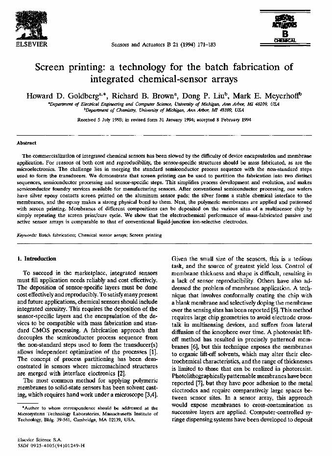
Fig. 15 is a schematic cross section of a single electrode site on the active multisensor chips (floorplans are
> E
a
1omM
Fig. 14. Response obtained from flow-injection analysis for the multi- site electrode.
H.D. GoIdbq et al. I Semors and Actuators B 21 (1994) 171-183 179
Polymer Membrane
M&d Layer Metal Layer
SOI Transisto Silicon Dioxide
Fig. 15. Cross section of asingle electrode site on the active multisensor
chips.
shown in Figs. 3 and 4). Signals from the individual ion-selective electrode sites feed directly below to the input transistors of the amplification circuitry. These integrated ion-selective electrodes are well suited for most multisensing applications, since they have linear transfer characteristics and allow a common solution potential (i.e., common reference electrode). These features stand in contrast to those of ISFETs, which have nonlinear transfer characteristics; to prevent this nonlinearity from being superimposed on the chemical response, a feedback circuit typically drives the gate electrode [3]. Since each device would need to drive the solution with a different potential, simultaneous operation of sensor arrays is prohibited unless supported with complicated electronics. Furthermore, thermal sen- sitivity and photoinduced junction leakage currents cause calibration drifts in ISFETs.
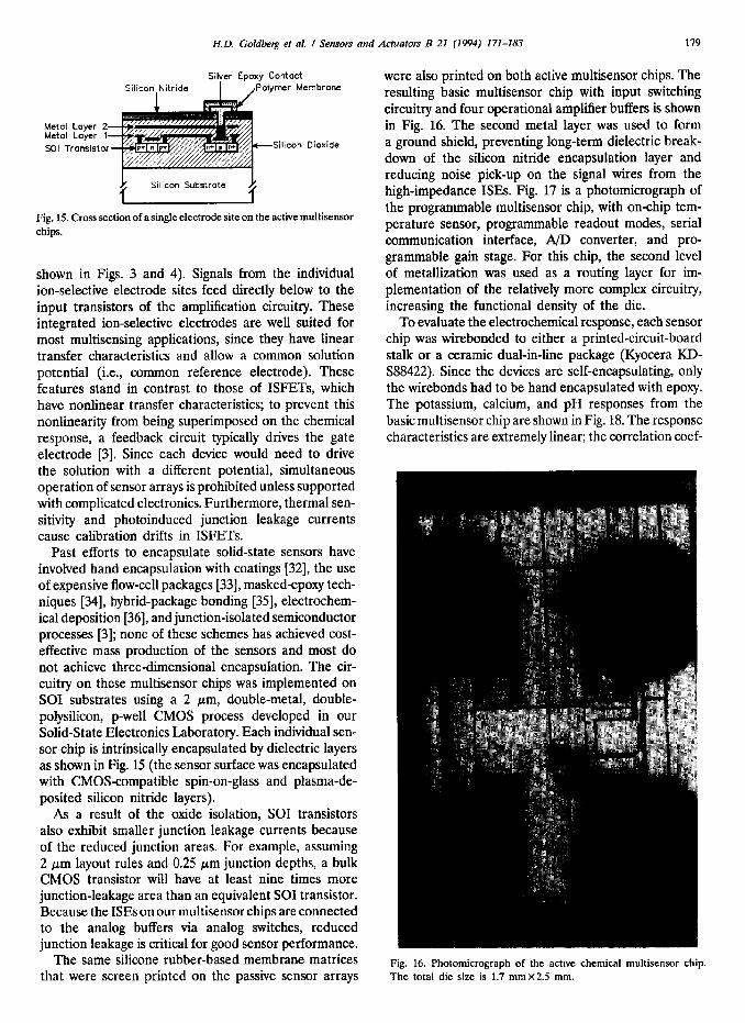
were also printed on both active multisensor chips. The resulting basic multisensor chip with input switching circuitry and four operational amplifier buffers is shown in Fig. 16. The second metal layer was used to form a ground shield, preventing long-term dielectric break- down of the silicon nitride encapsulation layer and reducing noise pick-up on the signal wires from the high-impedance ISEs. Fig. 17 is a photomicrograph of the programmable multisensor chip, with on-chip tem- perature sensor, programmable readout modes, serial communication interface, A/D converter, and pro- grammable gain stage. For this chip, the second level of metallization was used as a routing layer for im- plementation of the relatively more complex circuitry, increasing the functional density of the die.
To evaluate the electrochemical response, each sensor chip was wirebonded to either a printed-circuit-board stalk or a ceramic dual-in-line package (Kyocera KD- S88422). Since the devices are self-encapsulating, only the wirebonds had to be hand encapsulated with epoxy. The potassium, calcium, and pH responses from the basic multisensor chip are shown in Fig. 18. The response characteristics are extremely linear; the correlation coef-
Past efforts to encapsulate solid-state sensors have involved hand encapsulation with coatings [32], the use of expensive flow-cell packages [33], masked-epoxy tech- niques [34], hybrid-package bonding [35], electrochem- ical deposition [36], and junction-isolated semiconductor processes [3]; none of these schemes has achieved cost- effective mass production of the sensors and most do not achieve three-dimensional encapsulation. The cir- cuitry on these multisensor chips was implemented on SOI substrates using a 2 pm, double-metal, double- polysilicon, p-well CMOS process developed in our Solid-State Electronics Laboratory. Each individual sen- sor chip is intrinsically encapsulated by dielectric layers as shown in Fig. 15 (the sensor surface was encapsulated with CMOS-compatible spin-on-glass and plasma-de- posited silicon nitride layers).
As a result of the oxide isolation, SO1 transistors also exhibit smaller junction leakage currents because of the reduced junction areas. For example, assuming 2 km layout rules and 0.25 pm junction depths, a bulk CMOS transistor will have at least nine times more junction-leakage area than an equivalent SO1 transistor. Because the ISEs on our multisensor chips are connected to the analog buffers via analog switches, reduced junction leakage is critical for good sensor performance.
The same silicone rubber-based membrane matrices Fig. 16. Photomicrograph of the active chemical multisensor chip. that were screen printed on the passive sensor arrays The total die size is 1.7 mm x2.5 mm.

180 H.D. Goldberg et al. / Sensors and Achutors B 21 (1994) 171-183
Fig. 17. Photomicrograph of the programmable chemical sensor chip. The die size is 5.8 mm x 6.0 mm; the circuit includes 4917 transistors.
-1oc
F 5 -200
I co St 3
$ -3oc
2
-4oc
j9.2 mV/dacade
-7 -6 -5 -4 -3 -2
109 [concentration of K*, Ca+z,or H+](M)
Fig. 18. Multisensor chip potassium, calcium, and hydrogen ion responses. For comparison, the ideal Nemstian response of 59.2 mV/ decade is also shown.
ficients obtained from the linear regression analysis of the potassium, calcium, and pH responses are 1.000, 0.990, and 0.999, respectively. The potassium, calcium, and pH active sensor responses are 62.0 mV/decade, 20.3 mV/decade and 74 mV/decade, respectively. These electrochemical responses are comparable to those ob- tained from the passive chemical sensors, which illus- trates the reproducibility of the screen-printing tech- nique.
Fig. 19 shows both the measured sensor circuit re- sponse and the response calibrated for the analog offset drift of the system with temperature, using the oper- ational amplifier buffer input switching circuit with a constant voltage forced on the ISE input. A 1 mV change in the ISE signal as the result of circuit offset
1.398- l compensated sensor response •I D
s - 1.396- q
8 3 e
$ 1.394- D
.
1.390- . . .
. .
1.388i I I I . . 20 30 40 50 60
Temperature (C)
Fig. 19. Measured sensor circuit response vs. temperature and the circuit response with calibration for the analog offset drift.
60 -I 20 40 60 80 100120140160180200220
Temperature (C)
Fig. 20. Temperature sensor response.
corresponds to about a 4% change in concentration of the ion being monitored (assuming monovalent ion response). Similarly, the on-chip bandgap voltage ref- erence of the programmable sensor chip allows cali- bration for analog gain drifts with time and temperature. The linear 0.27 mVPC response of the on-chip tem- perature sensor is shown in Fig. 20; the gain of the on-chip instrumentation amplifier (G= 18) could be used to increase the overall response to 4.9 mV/“C. This capability of calilxating the electrochemical re- sponse for circuit- and temperature-induced effects results in sensors having greater accuracy and func- tionality which, in turn, allows them to address a larger range of potential applications.
5. Conclusions
The sensor-specific layers (silver epoxy solid-electrode contacts and polymeric membranes) were deposited after semiconductor processing with screen printing. This new sensor-fabrication methodology effectivelypar- titions the process flow into two distinct and decoupled

Fig. 21. Portion of an SOI CMOS w&r shkng the ~plcmcntation of two basic potentiometric chentkal wosnr arays (A}, a programs- able potentiometric chemical senwol array (B), and two amperometric chemical sensors (C).
sequences, making the process mare flexible and easing the technology transfer to industry. This approach allows various combinations of ion- and even bio-selective electrode sites to be implemented on a single multisensor chip. Screen printing even accommodates different types of chemical sensor arrays on a semiconductor wafer. For example, Fig. 21 is a photomicrograph of a portion of an SOI CMOS wafer containing two basic poten- tiametric chemical-sensor arrays, a programmable PC+ tentiometric chemical-sensor array, and hvo ampero- metric chemical sensors.
In coxlusion, the most significant result of this work is the development of a technology that allows the mass production of cost-effective sensor arrays as well as sophisticaled self-encapsulating integrated sensors. We believe that this will enable many industrial, environ- mental, and medical applications that need affordable, reliable, integrated chemical sensors.
Acknowledgments
We gratefully acknowledge the support of this work by Fleck Controls, Inc., Brookfield, WI, and by the National Science Foundation. Mr Robert W. Hawer and Mr Michael E. Poplawski were involved with various aspects of the SOI CMOS process development. Dr Guen Sig Cha did the initial membrane development and was involved with the initial characterization of the screen-printing process. We alsr, thank the KOPIN Corp. for generously providing the SO1 wafers used to fabricate our integrated sensors, and Mr Derryl Allman at the NCR Microelectronics Division for his assistance with the development of our spin-on-glass technology.
References
111 S.D. Senturia and R.L Smith, Microsensor packaging and system partitimkq, Sensors and Ackaotoq 25 (1988) 221-234.
R.B. Brown, Anintcgreti multiplc~nsarchemicaltransduar, RkD. 7W,’ Uniwsily of Utah, USA, Bne 1985. J. Kimurn, T. Kuriyama and Y. Ikwana, An integrated SOS/ FaT multi-bkensor and its application to medical use, Tech. Digq 3rd Inr. Cw$ StiSmte Sm and Actuatoq Tm- dwm ‘85 %il&&q PA, USA, 3w@ 7-9 I9q pp. 152-155. K. Bezcgh, k Bezegh, 6. Jan&q k Xu and W. Simm,
Multknsing ion-sclcctive Md-e&ct tramiators prepared by ionophore dopin technique&al chun.. 59 (19g7) 2@d&ZM8.
S. Nakamoto, N. ltn. T. Kuriyama and I. Khnura, A lift-off method for patterning ertzyme-immobilized membranes inmulti- bicwnsors, Senrors aRd Achlatcq 13 (198g) 16172. A. van den Berg. M. Koudelka-Hep, B, van &cr Schwt, E. Vcmcy-Norberg, P. Kxba, A. G&e1 and N. de R&j, An on- wafer fabricated frcc-chlorinc sensor, Tech. D&.T< 6~91 Iti Cm+
Soiid-StiteSmswmmf~dActuators (Tmnrriuc@rs ‘91, SmFrm~ircq
CA, us.4, June 24-B, 1w> pp_ xv-23#. S, Anna, C. Li, 2. Zhilong, 1. Luna and C. Kerning, An IC- kbnokgy compatible automatic method (SCZ method) for immobilizatjon membranes, Smwm and ACIUM~, BI (1990) 51&517.
S.N. Colette, G. Davis, J. Itak, 1. Lauks, R. Mier, S. Ptiik, N. Smit, S. Steiner, P. van dcr Wcrf and H. W&k. Method of manufacturing a pfwality of uniform microfabricated sensing devices having an immobilized @and receptor, m Patent No, 50 063 QBI (NW. 5, 1991). B.D. Goldbqg, G-S. Cha, R.W. Hewer and R.B. Bmm, Batch fabrication of solid&ate ions&xtive ~onsors, T&. LB&S& 3rd
Itt~ M&&g Chemkal S&wrs, Ckveknd OH, USA, Sep~ I%?, pp. P31-P32.
P.W. Kulesza, RH. Es~es and K. Spa@, A screen-printable @ybnick mating for silicon wfcrs, SaLid S#& re&tc& 3i {1988) 135139.
H.D. Goldberg. G.S. Cha and R.B. Brown, ion-selective senwrs inwporatmg strong@ adhesive polymeric membranes, TKh, D&@ IEEE SOISOY amdAuu&or Wodwhop, H&n Head bIanc$ SC, USA, Ju?E zwo, pp. 16%172.
H.D. Goldberg, G.S. Char D.P. Llu, M.E. Meyerhoff and R.B. Brown, Improved stability at the polymeric membrrm&olid- contact interface of solid-state potentiometric btt-ge~~ors, Tech. D&t, 6th hr. Conj Salid-S&te Senwr~ and Actwuors ~mnr- dwce~ ‘WI), San Fmncisco, CA, tISr4, June 24-28, INI, pp. 781-784.
G.S. Cha, D. Liu, ME. Meyerhoff, H.C, Cantor, AR. Midgley, H.D. GoIdbcrg and R.B. Brows, Ekctrmhemical performance, biaampatibility, and adhesion of new polymer matrices for wkhtate ion wxwv~s, AnaL Chem., 63 (1991) M&1672. H,D. Goldberg, D.P. Liu, R.W. Howcr, M.E. Foplawski and R.B. Brown, Screen printing: a te&nology for partitioning integrated microsensor prtxzssing, T&I. D&w, JE.EE SW
arsd Achrnlw WorWwj7, HiSton IImd Is.4~14 SC, USA, Jw IWZ, pp. l&143.
R.B. Brcwo, G.S. Cha and H.D. Goldberg, Batch depc=sition of po@neric ion sco8or membranes, Crs and Inr. Parent Pmding +g. 24 1Wl). R.E. Belford. kE. Owen and R.G. Kelly, Thii-film hybrid pH sensors, Sm and Actuatoss, 11 (1%‘) 387-398.
S-8. Yee and ht.A, Mromowitz. in P.W. Cheung, D.G. Fleming. h8.R Neuman and W.H. Ko (eda), Tkwy, &s&n andBiotnedicu! Appficbwas of S&i Sfafe Chwnicd Xxwrx, CRC Press, 3m Raton, FL. 1977, pp. 81-87.

H.D. GoldbeT et 01. / Ser~~rx and Actuatom B 21 (1994) 171-183 182
P91
PO1
PI
[221
1261
t*71
I281
P91
1301
[311
[321
1331
[341
I351
1361
S.I. Lepptivuori and P.S. Romppainen, The use of hybrid microelectronics in the construction of ion-selective electrodes,
Ekctnxompment Sci. Technol., 10 (1983) 129-133. SA. Wring, J.P. Hart and B.J. Birch, Voltammetric behavior of screen-printed carbon electrodes, chemically modified with selected mediators, and their application as sensors for the determination of reduced glutathione, AnarySr, I16 (1991) X&129. D.H. Craston, C.P. Jones, D.E Williams and N.E. Murr, Microband electrodes fabricated by screen printing processes: applications in electroanalysis, Z&mm, 38 (1991) 17-26. C.S. Cha, M.J. Shao and C.C. Liu, Electrochemical behavior of microfabricated thick-film electrodes, Sensors and Actialors E, 2 (1990) 277-281. RE. Trease and R.L. Die&, Rheology of pastes in thick-film printing, solid-s~are TechnoL, (Jan.) (1972) 39-43.
L.F. Miller, Screenability and rheology, Solid-&ate TechnoL, (Oct.) (1974) %-6o. N. Hampp, C Eppelsheim, J. Popp, M. Bisenberg and C. BrBucNe, Design and application of thick-film multisensors, Sensors and Actuators A, 31 (1992) 144-148. T. Matsuo and H. Nakajima, Characteristics of reference elec- trodcs using a polymer gate, Sensors and Actuators, 5 (1984) 293-305. S. Yee, H. Sin and I_ Lam, Miniature liquid junction reference electrode with micromachined silicon cavity, Sensors and Ac- tuators, I5 (1988) 337-345. RL. Smith and D.C. Scott, An integrated sensor for electro- chemical measurements, IEE Trans. Biomed. En&=., BME-33 (1966) 83-W. C.P. Wang, High performance screen printable silicone as selective hybrid IC encapsulant, IEEE Trans. Components, Hy- brids, Manufact. Tech& CHMT-13 (1990) 759-765. Y, Sane, Advanced polyimide passivation technology on semi- conductor wafer by screen printing method, Ep-Tek Tech. Seminar ‘89, Egasy Technology Inc., Billerica, MA, USA, June 21, 1989, pp. 1-13. Y. Umezawa (ed.), CRC Handbook of Ion-Selective Electrodes: Selecrivity Cc@icienfs, CRC Press, Boca Raton, 1990. A_ Sibbald, P.D. Whalley and A.K. Covington, A miniature flow-through cell with a four-function CHEMFET integrated circuit for simultaneous measurements of potassium, hydrogen, calcium and sodium ions, Anal. Chim. Acfa, 159 (1984) 47-62. I.R. I-auks, MR. Groves and H.J. Wieck, Mass fabricated ion, gas, and enzyme multispecies sensors using IC technology, Proc. Symp. Electmctwnical Sensors Bkmed. Appl., Boston. h&4, USA, 1986, pp. 116-128. N. Ho, J. Kratochvil, G. Blackbum and J. Jinata, Encapsulation of polymeric membrane-based ion-selective field-effect tran- sistors, Senws and Acfuotm, 4 (1983) 413-421. H. van den Vlekkert, M. Decroux and N. de Rooij, Glass encapsulation of chemical solid state sensors based on anodic bonding, Tech. Digest, 4th Znt. ConfI S&i-Stare Sensors and
Actuators (Transducers ‘87), Tokyo, Japan, June 2-5, 1987, pp. 730-733. K. Potje-Kamloth, P. Jinata, J. Jinata and M. Josowicz, Elec- trochemical encapsulation for sensors, Sensors and Actuators 18 (1989) 415-425.
Biographies
Howard D. Goldberg received his B.S. degree in electrical engineering from Lehigh University in 1987.
He received his M.S. degree (1989) and his Ph.D. (1993) in electrical engineering, with an emphasis on solid- state electronics, from the University of Michigan. His Ph.D. work was concerned with improving the reliability and lifetimes of solid-contact potentiometric chemical sensors as well as the development of a new mass- fabrication sequence for integrated solid-state chemical- sensor arrays with on-chip analog and digital circuitry. Howard is currently a postdoctoral associate at the Microsystems Technology Laboratories at the Massa- chusetts Institute of Technology. His current research interests involve the design and fabrication of novel micromechanical sensors and actuators.
Richard B. Brown received B.S. and MS. degrees in electrical engineering from Brigham Young University in 1976. From 1976 to 1981 he worked in computer design as vice-president research and development at Holman Industries, Oakdale, CA, and then as manager of computer development at Cardinal Industries, Webb City, MO. Richard received an electrical engineering Ph.D. at the University of Utah in 1985. His Ph.D. work was in the area of solid-state chemical sensors, which included development of a custom MOS fab- rication process and integration of multiple transducers with analog and digital circuitry. in September 1985, he joined the University of Michigan Department of Electrical Engineering and Computer Science faculty. He has been involved in shaping the VLSI program there and introducing a uniform set of electronic CAD tools into the curriculum. His areas of current research are high-speed digital integrated circuits and solid-state sensors.
Dong P. Liu received her B.S. degree in chemistry from the University of Science and Technology of China in 1986. In 1989, she received her M.S. in medicinal chemistry from Beijing Medical University. She is cur- rently working toward her Ph.D. degree in electro- analytical chemistry at the University of Michigan, under the guidance of Professor Mark E. Meyerhoff.
Murk E. Meyerhafl, professor of chemistry at the University of Michigan, received his B.A. degree in chemistry from the Herbert H. Lehman College (SUNY System) in 1974 and his Ph.D. degree from the State University of New York at Buffalo in 1979. Following a brief period as a postdoctoral fellow at the University of Delaware, he joined the faculty at Michigan as an assistant professor in the Fall of 1979. His research interests are in the field of analytical chemistry, par- ticularly the development of new ion-, gas-, and bio- selective electrochemical sensors suitable for clinical and environmental measurements. He also has active

H.D. Goldberg et al. I Sensors and Actuators B 21 (1994) 171-183 183
research programs in the analytical areas of enzyme- linked competitive binding assays and ion-chromato- graphy. He has authored or co-authored more than 100 original research articles on these subjects and is on the editorial or advisory boards of several journals
devoted to the field of analytical chemistry. He is a member of the American Chemical Society, the Amer- ican Association for the Advancement of Science, the American Association of Clinical Chemists, and the Alpha Chi Sigma Chemical Fraternity.