scm-i.mx 6quad module - fact sheet - nxp semiconductors · scm-i.mx 6dual/6quad packaging...
TRANSCRIPT
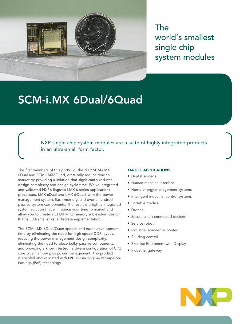
The world’s smallest single chip system modules
NXP single chip system modules are a suite of highly integrated products in an ultra-small form factor.
SCM-i.MX 6Dual/6Quad
The first members of this portfolio, the NXP SCM-i.MX 6Dual and SCM-i.MX6Quad, drastically reduce time to market by providing a solution that significantly reduces design complexity and design cycle time. We’ve integrated and validated NXP’s flagship i.MX 6 series applications processors, i.MX 6Dual and i.MX 6Quad, with the power management system, flash memory, and over a hundred passive system components. The result is a tightly integrated system solution that will reduce your time to market and allow you to create a CPU/PMIC/memory sub-system design that is 50% smaller vs. a discrete implementation.
The SCM-i.MX 6Dual/Quad speeds and eases development time by eliminating the need for high-speed DDR layout, reducing the power management design complexity, eliminating the need to place bulky passive components, and providing a known tested hardware configuration of CPU core plus memory plus power management. The product is enabled and validated with LPDDR2 memory via Package-on-Package (PoP) technology.
TARGET APPLICATIONS
Digital signage
Human-machine interface
Home energy management systems
Intelligent industrial control systems
Portable medical
Drones
Secure smart connected devices
Service robot
Industrial scanner or printer
Building control
Exercise Equipment with Display
Industrial gateway
SCM-i.MX 6DUAL/6QUAD PACKAGING TECHNOLOGY
The SCM packaging technology allows the build-out of highly integrated devices in an incredibly small footprint. At 14mm x 17mm x 1.7mm the package is smaller than a US dime. In addition, the SCM- i.MX 6Dual/6Quad package is designed to enable LPDDR2 memory via Package-on-Package (PoP) configuration. This provides advantages not just in the elimination of high-speed memory design layout, but provides additional benefit in terms of PCBarea size, enabling you to create ultra-compact designs and/or more feature-packed products. New to Package-on-Package technology? We have partners that can help you assemble your own PoP designs or you can order pre-stacked SCM devices through Arrow Electronics.
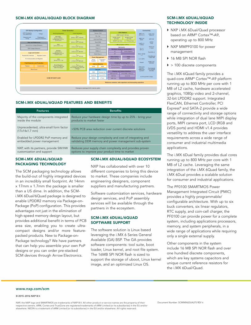
Keypad
Clock and Reset
Smart DMA
IOMUX
Timer x 3
PWM x 4
Watch Dog x 2
MMC 4.4/SD 3.0 x 3
MMC 4.4/SDXC
UART x 5,5 Mbit/s
MIPI HSI
S/PDIFTx/Rx
PCIe® 2.0(1-lane)I2C x 3,
SPI x 5
ESAI, I2S/SSIx 3
3.3 V GPIO
Keypad
USB2 OTG and PHY
USB2 Host and PHY
System Control Connectivity
Multimedia
TrustZone®
Ciphers
RNG Security Cntrl.
TemperatureMonitor
PowerSupplies
Secure RTC
eFuses
Power Management
ROM RAM
Internal Memory
Security
Hardware Graphics Accelerators
Vector Graphics3D
2DFlexCAN x 2
1Gbit Ethernet+ IEEE 1588
NAND Cntrl.(BCH40)
S-ATA and PHY 3 Gbps
Dual-channelx 32 LPDDR2
400 MHz
USB2 HSICHost x 2
1080p30 Enc/Dec ASRCVideo Codecs Audio
Imaging Processing UnitResizing & Blending
Inversion/Rotation
Image Enhancement
Display and Camera Interface
HDMI and PHY
MIPI DSI
MIPI CSI2
20-bit CSI
ARM® Cortex®–A9 Core
32 KB I-Cacheper Core
Secure JTAG
PLL, Osc
NEONTM per Core
32 KB D-Cacheper Core
PTM per Core
CPU Platform
1 MB L2-Cache + VFPv3
24-bit RGB, LVDS (x 2)
OTP Startup Configuration Power Generation
Switching Regulators
SW1A/B/C (0.3 to 1.875 V)
Configurable 4.5 A or 2.5 A+2.0 A
SW2(0.4 to 3.3 V, 2 A)
SW3A/B(0.4 to 3.3 V)
Configurable 2.5 A or 1.25 A+1.25 A
SW4(0.4 to 3.3 V, 1 A)
Boost Regulator(5 to 5.15 V, 600 mA)
USB OTG Supply
Linear Regulators
VGEN1(0.8 to 1.55 V, 100 mA)
VGEN2(0.8 to 1.55 V, 250 mA)
VGEN3(1.8 to 3.3 V, 100 mA)
VGEN4(1.8 to 3.3 V, 350 mA)
VGEN5(1.8 to 3.3 V, 100 mA)
VGEN6(1.8 to 3.3 V, 200 mA)
VSNVS(1.0 to 3.0 V, 400 µA)
RTC Supply with Coin Cell Charger
OTP Prototyping (Try before buy) Voltage
Sequence and Timing
Phasing andFrequency Selection
DDR Voltage Reference
Parallel MCU Interface
Thermal Current Limit
Short Circuit
16 MB SPI NOR FLASH
Package-on-package (PoP) memory option
Reference resistors, bulk capacitors and decoupling capacitors
Regulator Control
I2C Communication and Registers
Internal Core Voltage Reference
Bias and References
Logic and Control
Fault Detection and Protection
SCM-i.MX 6QUAD BLOCK DIAGRAMSCM-i.MX 6DUAL/6QUAD BLOCK DIAGRAM
SCM-i.MX 6DUAL/6QUAD FEATURES AND BENEFITS
Features Benefits
Majority of the components integrated inside the module
Reduce your hardware design time by up to 25% - bring your products to market faster
Unprecedented, ultra-small form factor (17x14x1.7 mm) >50% PCB area reduction over current discrete solutions
Enabled for LPDDR2 PoP memory and embedded power management
Reduce your design complexity and cost of integrating and validating DDR memory and power management sub-system
NXP, with its partners, provide SW/HW customization and support
Reduces your supply chain complexity and provides proven options to improve your product time to market
SCM-i.MX 6DUAL/6QUAD ECOSYSTEM
NXP has collaborated with over 10 different companies to bring this device to market. These companies include engineering designers, component suppliers and manufacturing partners.
Software customization services, hardware design services, and PoP assembly services will be available through the partners in the ecosystem.
SCM-i.MX 6DUAL/6QUAD SOFTWARE SUPPORT
The software solution is Linux based leveraging the i.MX 6 Series General Available (GA) BSP. The GA provides software components: tool suite, boot loader, Linux kernel, and root file system. The 16MB SPI NOR flash is sized to support the storage of uboot, Linux kernel image, and an optimized Linux OS.
SCM-i.MX 6DUAL/6QUAD TECHNOLOGY INSIDE
NXP i.MX 6Dual/Quad processor based on ARM® Cortex™-A9, operating up to 800 MHz
NXP MMPF0100 for power management
16 MB SPI NOR flash
> 100 discrete components
The i.MX 6Quad family provides a quad-core ARM® Cortex™-A9 platform running up to 800 MHz per core with 1 MB of L2 cache, hardware accelerated graphics, 1080p video and 2-channel, 32-bit LPDDR2 support. Integrated FlexCAN, Ethernet Controller, PCI Express® and SATA-2 provide a wide range of connectivity and storage options while integration of dual lane MIPI display ports, MIPI camera port, LCD (RGB and LVDS ports) and HDMI v1.4 provides versatility to address the user interface requirements across a wide range of consumer and industrial multimedia applications.
The i.MX 6Dual family provides dual cores running up to 800 MHz per core with 1 MB of L2 cache. Leveraging the same integration of the i.MX 6Quad family, the i.MX 6Dual provides a scalable solutionfor consumer and industrial applications.
The PF0100 SMARTMOS Power Management Integrated Circuit (PMIC) provides a highly programmable/ configurable architecture. With up to six buck converters, six linear regulators, RTC supply, and coin-cell charger, the PF0100 can provide power for a complete system, including applications processors, memory, and system peripherals, in a wide range of applications while requiring only a single external supply.
Other components in the system include 16 MB SPI NOR flash and over one hundred discrete components, which are key systems capacitors and unique current reference resistors for the i.MX 6Dual/Quad.
www.nxp.com/scm
© 2015–2016 NXP B.V.
NXP, the NXP logo and SMARTMOS are trademarks of NXP B.V. All other product or service names are the property of their respective owners. ARM, Cortex and TrustZone are registered trademarks of ARM Limited (or its subsidiaries) in the EU and/or elsewhere. NEON is a trademark of ARM Limited (or its subsidiaries) in the EU and/or elsewhere. All rights reserved.
Document Number: SCMIMX6DUALFS REV 4