scilab textbook companion for electronics fundamentals and
TRANSCRIPT

Scilab Textbook Companion forElectronics Fundamentals and Applicationsby D. Chattopadhyay and P. C. Rakshit1
Created byShreeja Lakhlani
B.TechOthers
Dharamsinh Desai UniversityCollege Teacher
Prof. Prarthan. D. MehtaCross-Checked byBhavani Jalkrish
July 31, 2019
1Funded by a grant from the National Mission on Education through ICT,http://spoken-tutorial.org/NMEICT-Intro. This Textbook Companion and Scilabcodes written in it can be downloaded from the ”Textbook Companion Project”section at the website http://scilab.in

Book Description
Title: Electronics Fundamentals and Applications
Author: D. Chattopadhyay and P. C. Rakshit
Publisher: New Age International, New Delhi
Edition: 8
Year: 2007
ISBN: 81-224-2093-1
1

Scilab numbering policy used in this document and the relation to theabove book.
Exa Example (Solved example)
Eqn Equation (Particular equation of the above book)
AP Appendix to Example(Scilab Code that is an Appednix to a particularExample of the above book)
For example, Exa 3.51 means solved example 3.51 of this book. Sec 2.3 meansa scilab code whose theory is explained in Section 2.3 of the book.
2

Contents
List of Scilab Codes 4
1 Basic Ideas Energy Bands In Solids 5
2 Electron Emission from Solid 7
3 PROPERTIES OF SEMICONDUCTORS 11
4 Metal Semiconductor Contacts 17
5 Semiconductor Junction Diodes 21
6 Diode Circuits 30
7 Junction Transistor Characteristics 36
8 Junction Transistors Biasing and Amplification 44
9 Basic Voltage and Power Amplifiers 63
10 Feedback In Amplifiers 71
11 Sinusoidal Oscillators and Multivibrators 76
12 Modulation and Demodulation 81
3
13 Field Effect Transistors 86
14 Integrated Circuits and Operational Amplifiers 100
15 Active Filters 107
16 Special Devices 112
17 Number Systems Boolean Algebra and Digital Circuits 113
19 VLSI Technology and Circuits 122
20 Cathode Ray Oscilloscope 127
21 Communication Systems 132
23 Lasers Fibre Optics and Holography 135
4

List of Scilab Codes
Exa 1.7.1 To find the final velocity of electron . . . . . 5Exa 1.7.2 To find the velocity and kinetic energy of ion 5Exa 2.7.1 to calculate the number of electrons emitted
per unit area per second . . . . . . . . . . . 7Exa 2.7.2 To find the percentage change in emission cur-
rent . . . . . . . . . . . . . . . . . . . . . . 8Exa 2.7.3 difference between thermionic work function
of the two emitters . . . . . . . . . . . . . . 8Exa 2.7.4 to find the anode voltage . . . . . . . . . . . 9Exa 3.11.1 To find the conductivity and resistivity . . . 11Exa 3.11.2 To find Concentration of donor atoms . . . . 12Exa 3.11.4 To find intrinsic conductivity and resistance
required . . . . . . . . . . . . . . . . . . . . 12Exa 3.11.5 To find the conductivity and current density
of doped sample . . . . . . . . . . . . . . . . 13Exa 3.11.6 To find the electron and hole concentration
and conductivity of doped sample . . . . . . 14Exa 3.11.7 To find the required wavelength . . . . . . . 15Exa 3.11.8 To find the magnetic and hall field . . . . . 15Exa 4.7.1 to find barrier height and depletion region
width and maximum electric field . . . . . 17Exa 4.7.2 to find the barrier height and concentration 18Exa 4.7.3 to calculate barrier lowering and the position
of the maximum barrier height . . . . . . . 18Exa 4.7.4 to determine the effective richardson constant 19Exa 4.7.5 to calculate current in a Schottky diode . . 19Exa 5.7.1 To find the voltage to be applied across the
junction . . . . . . . . . . . . . . . . . . . . 21
5
Exa 5.7.2 To calculate the ratio of current for forwardbias to that of reverse bias . . . . . . . . . . 22
Exa 5.7.3 To determine the static and dynamic resis-tance of the diode . . . . . . . . . . . . . . . 22
Exa 5.7.4 To calculate the increase in the bias voltage 23Exa 5.7.5 To find the bias voltage of pn junction diode 23Exa 5.7.6 To calculate the rise in temperature . . . . . 24Exa 5.7.7 To calculate the maximum permissible bat-
tery voltage . . . . . . . . . . . . . . . . . . 25Exa 5.7.8 To calculate series resistance and the range
over which load resistance can be varied . . 25Exa 5.7.9 To determine the limits between which the
supply voltage can vary . . . . . . . . . . . 26Exa 5.7.10 To find whether power dissipated exceeds the
maximum power limit . . . . . . . . . . . . 27Exa 5.7.11 To determine the range of variation of the
output voltage . . . . . . . . . . . . . . . . 28Exa 5.7.12 To find the value of resistance R . . . . . . . 29Exa 6.11.1 To find various currents voltages power con-
version efficiency and percentage regulation 30Exa 6.11.2 To find various currents power ripple voltage
percentage regulation and effiiciency of recti-fication . . . . . . . . . . . . . . . . . . . . 31
Exa 6.11.3 To calculate the dc load voltage ripple voltageand the percentage regulation . . . . . . . . 32
Exa 6.11.4 To calculate ripple voltage and the percentageripple . . . . . . . . . . . . . . . . . . . . . 33
Exa 6.11.5 To design a full wave rectifier with L type LCfilter . . . . . . . . . . . . . . . . . . . . . . 34
Exa 7.13.1 To find the voltage gain and power gain of atransistor . . . . . . . . . . . . . . . . . . . 36
Exa 7.13.2 To find the base and collector current of agiven transistor . . . . . . . . . . . . . . . . 37
Exa 7.13.3 To calculate the emitter and collector currentof a given transistor . . . . . . . . . . . . . 37
Exa 7.13.4 To calculate the voltage between collector andemitter terminals . . . . . . . . . . . . . . . 38
6
Exa 7.13.5 To check what happens if resistance Rc is in-definitely increased . . . . . . . . . . . . . . 39
Exa 7.13.6 To check whether transistor is operating inthe saturation region for the given hFE . . 40
Exa 7.13.7 To calculate the output resistance along withthe current gain . . . . . . . . . . . . . . . . 41
Exa 7.13.8 To find the resistance R1 R2 and the range ofRL . . . . . . . . . . . . . . . . . . . . . . . 42
Exa 8.14.1 To find the Q point and stability factors . . 44Exa 8.14.2 To find the resistances R1 R2 and Re . . . . 45Exa 8.14.3 To calculate the input and output resistances
and current voltage and power gain . . . . . 46Exa 8.14.4 To find the input and output resistance . . . 47Exa 8.14.5 To find the current amplification and voltage
and power gains . . . . . . . . . . . . . . . . 48Exa 8.14.6 To determine the current and voltage gain as
well as the input and output resistances . . 49Exa 8.14.7 To determine the input and output resistances
as well as the voltage gain and Q point . . . 50Exa 8.14.8 To design a CE transistor amplifier . . . . . 51Exa 8.14.9 To find the resistance R1 . . . . . . . . . . . 54Exa 8.14.10 To find the quiescent values of IE and VCE 55Exa 8.14.11 To calculate the quiescent values of IB IC IE
and VCE . . . . . . . . . . . . . . . . . . . 56Exa 8.14.12 To determine the operating point . . . . . . 58Exa 8.14.13 To determine the operating point . . . . . . 59Exa 8.14.14 To determine the ac as well as dc load line
and the amplitude of the output voltage . . 60Exa 9.12.1 To determine the lower and upper half power
frequencies . . . . . . . . . . . . . . . . . . 63Exa 9.12.2 To determine the lower and upper half power
frequencies . . . . . . . . . . . . . . . . . . 64Exa 9.12.3 To find the gain relative to the mid frequency
gain . . . . . . . . . . . . . . . . . . . . . . 65Exa 9.12.4 To calculate the output power . . . . . . . . 66Exa 9.12.5 To calculate dc input and ac output power
along with the collector dissipation and theefficiency . . . . . . . . . . . . . . . . . . . . 67
7

Exa 9.12.6 To determine the maximum dc power and themaximum output power along with the effi-ciency . . . . . . . . . . . . . . . . . . . . . 67
Exa 9.12.7 To calculate the resonant frequency along withthe bandwidth and the maximum voltage gain 68
Exa 9.12.8 To find out the decibel change in the outputpower level . . . . . . . . . . . . . . . . . . 69
Exa 9.12.9 To find the rms output voltage and rms inputvoltage along with the output power in themidband region . . . . . . . . . . . . . . . . 70
Exa 10.7.1 To find the voltage gain with feedback theamount of feedback in dB the output voltageof the feedback amplifier the feedback factorthe feedback voltage . . . . . . . . . . . . . 71
Exa 10.7.2 To find the minimum value of the feedbackratio and the open loop gain . . . . . . . . . 72
Exa 10.7.3 To find the reverse transmission factor . . . 72Exa 10.7.4 To find voltages current and power dissipa-
tion of a given transistor circuit . . . . . . . 73Exa 10.7.5 To calculate the voltage gain and input out-
put resistances . . . . . . . . . . . . . . . . 74Exa 11.12.1 To calculate the frequency of oscillation and
mutual inductance . . . . . . . . . . . . . . 76Exa 11.12.2 To find the values of the inductances . . . . 77Exa 11.12.3 To calculate the frequency of oscillation . . 78Exa 11.12.4 To determine the frequency of oscillation . 78Exa 11.12.5 To find the resistances needed to span the fre-
quency range and to find the ratio of the re-sistances . . . . . . . . . . . . . . . . . . . 79
Exa 11.12.6 To find the quality factor of the crystal . . . 80Exa 12.9.1 To find the percentage modulation and the
amplitude of the unmodulated carrier . . . 81Exa 12.9.2 To find the frequency span of each sideband
and maximum upper and minimum lower sidefrequency along with the channelwidth . . . 82
Exa 12.9.3 To calculate the power developed by an AMwave . . . . . . . . . . . . . . . . . . . . . . 82
Exa 12.9.4 To determine the necessary audio power . . 83
8
Exa 12.9.5 To find the modulation index three pairs ofside frequency and the channelwidth . . . . 83
Exa 12.9.6 To find the highest modulation frequency . . 84Exa 12.9.7 To find the depth of modulation and the total
radiated power . . . . . . . . . . . . . . . . 85Exa 13.16.1 To find the pinch off voltage and the satura-
tion voltage . . . . . . . . . . . . . . . . . . 86Exa 13.16.2 To find the resistance RS . . . . . . . . . . . 87Exa 13.16.3 To find the transconductance of the FET along
with the amplification factor . . . . . . . . . 87Exa 13.16.4 To calculate the voltage gain and the output
resistance . . . . . . . . . . . . . . . . . . . 88Exa 13.16.5 To find the drain current and the pinch off
voltage . . . . . . . . . . . . . . . . . . . . . 88Exa 13.16.6 To determine drain current along with drain
source voltage along with gate source voltage 89Exa 13.16.7 To calculate the drain current . . . . . . . 91Exa 13.16.8 To find the saturation drain current and the
minimum value of drain source voltage . . . 92Exa 13.16.9 To determine gate source voltage and the transcon-
ductance . . . . . . . . . . . . . . . . . . . . 93Exa 13.16.10 To find the gate source voltage . . . . . . . 94Exa 13.16.11 To calculate Rs and the channel resistance . 94Exa 13.16.12 To find the saturation drain current . . . . . 95Exa 13.16.13 To calculate drain current along with gate
source voltage and drain source voltage . . . 96Exa 13.16.14 To calculate K along with drain current and
drain source voltage . . . . . . . . . . . . . 96Exa 13.16.15 To calculate the voltage gain and the output
resistance . . . . . . . . . . . . . . . . . . . 97Exa 13.16.16 To find the small signal voltage gain . . . . 98Exa 14.12.1 To determine the output voltage along with
input resistance and the input current . . . 100Exa 14.12.2 To calculate the voltage gain . . . . . . . . . 101Exa 14.12.3 To calculate the voltage gains for difference
and common mode signals along with CMRR 101Exa 14.12.4 To find the output voltage of the three input
summing amplifier . . . . . . . . . . . . . . 102
9

Exa 14.12.5 To find the voltage gain along with the outputvoltage . . . . . . . . . . . . . . . . . . . . . 103
Exa 14.12.6 To find the output voltage of the differentiator 104Exa 14.12.8 To calculate the output voltage . . . . . . . 105Exa 14.12.9 To find the differential mode gain . . . . . . 106Exa 15.7.1 To design a Butterworth low pass filter . . . 107Exa 15.7.2 To design a first order Butterworth active High
Pass filter . . . . . . . . . . . . . . . . . . . 108Exa 15.7.3 To design a second order band pass Butter-
worth filter . . . . . . . . . . . . . . . . . . 109Exa 15.7.4 To design a notch filter . . . . . . . . . . . . 110Exa 16.10.1 To determine the time period of the sawtooth
voltage across capacitor C . . . . . . . . . . 112Exa 17.17.1 To determine the binary equivalents . . . . 113Exa 17.17.2 To determine the decimal equivalent . . . . 113Exa 17.17.3 To convert from binary system to decimal sys-
tem . . . . . . . . . . . . . . . . . . . . . . 114Exa 17.17.4 To convert from decimal system to binary sys-
tem . . . . . . . . . . . . . . . . . . . . . . 115Exa 17.17.5 To find the equivalent of given number in a
code base 5 . . . . . . . . . . . . . . . . . . 116Exa 17.17.6 To perform binary addition corresponding to
decimal addition . . . . . . . . . . . . . . . 117Exa 17.17.7 To perform binary addition and also to show
the corresponding decimal addition . . . . . 117Exa 17.17.8 To perform the binary subtraction . . . . . 118Exa 17.17.9 To obtain the output levels of a silicon tran-
sistor for given input levels and to show thatcircuit has performed NOT operation usingpositive logic . . . . . . . . . . . . . . . . . 118
Exa 17.17.10 To solve the Boolean expression . . . . . . . 120Exa 19.29.1 To find the value of inverse of aspect ratio
along with power dissipated and load resis-tance . . . . . . . . . . . . . . . . . . . . . . 122
Exa 19.29.2 To find the pull up and pull down aspect ratio 123Exa 19.29.3 To find the value of inverse of aspect ratio
of the PMOS transistor for a symmetrical in-verter . . . . . . . . . . . . . . . . . . . . . 123
10
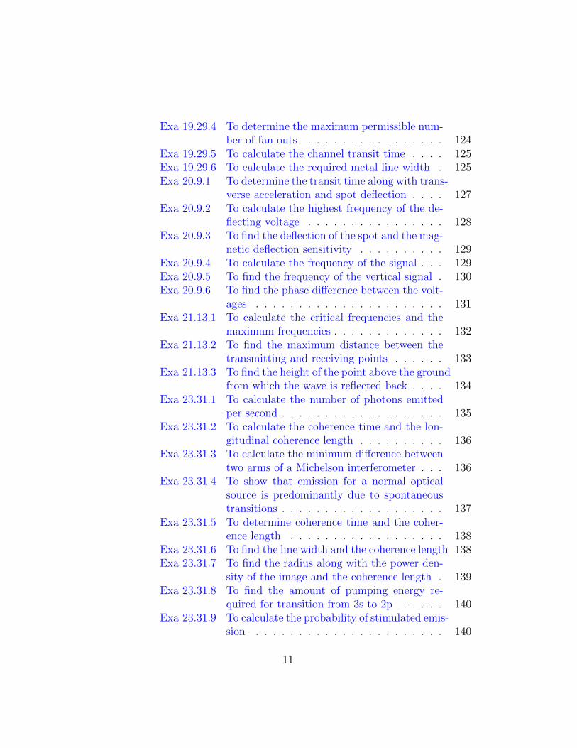
Exa 19.29.4 To determine the maximum permissible num-ber of fan outs . . . . . . . . . . . . . . . . 124
Exa 19.29.5 To calculate the channel transit time . . . . 125Exa 19.29.6 To calculate the required metal line width . 125Exa 20.9.1 To determine the transit time along with trans-
verse acceleration and spot deflection . . . . 127Exa 20.9.2 To calculate the highest frequency of the de-
flecting voltage . . . . . . . . . . . . . . . . 128Exa 20.9.3 To find the deflection of the spot and the mag-
netic deflection sensitivity . . . . . . . . . . 129Exa 20.9.4 To calculate the frequency of the signal . . . 129Exa 20.9.5 To find the frequency of the vertical signal . 130Exa 20.9.6 To find the phase difference between the volt-
ages . . . . . . . . . . . . . . . . . . . . . . 131Exa 21.13.1 To calculate the critical frequencies and the
maximum frequencies . . . . . . . . . . . . . 132Exa 21.13.2 To find the maximum distance between the
transmitting and receiving points . . . . . . 133Exa 21.13.3 To find the height of the point above the ground
from which the wave is reflected back . . . . 134Exa 23.31.1 To calculate the number of photons emitted
per second . . . . . . . . . . . . . . . . . . . 135Exa 23.31.2 To calculate the coherence time and the lon-
gitudinal coherence length . . . . . . . . . . 136Exa 23.31.3 To calculate the minimum difference between
two arms of a Michelson interferometer . . . 136Exa 23.31.4 To show that emission for a normal optical
source is predominantly due to spontaneoustransitions . . . . . . . . . . . . . . . . . . . 137
Exa 23.31.5 To determine coherence time and the coher-ence length . . . . . . . . . . . . . . . . . . 138
Exa 23.31.6 To find the line width and the coherence length 138Exa 23.31.7 To find the radius along with the power den-
sity of the image and the coherence length . 139Exa 23.31.8 To find the amount of pumping energy re-
quired for transition from 3s to 2p . . . . . 140Exa 23.31.9 To calculate the probability of stimulated emis-
sion . . . . . . . . . . . . . . . . . . . . . . 140
11

Exa 23.31.10 To calculate the NA and the acceptance anglealong with number of reflections per metre . 141
12

Chapter 1
Basic Ideas Energy Bands InSolids
Scilab code Exa 1.7.1 To find the final velocity of electron
1
2 // s c i l a b 5 . 4 . 13 // windows 7 o p e r a t i n g system4 // c h a p t e r 1 : Ba s i c I d e a s : Energy Bands In S o l i d s5 clc
6 clear
7 // g i v e n8 Ek =1.6*(10^ -19) *100; //Ek=f i n a l k i n e t i c ene rgy o f
e l e c t r o n i n J o u l e s9 m0 =9.11*(10^ -31);//m0=r e s t mass o f the e l e c t r o n i n
kg10 // s o l v i n g f i n a l v e l o c i t y o f the e l e c t r o n11 v=sqrt ((2*Ek)/m0)//v=f i n a l v e l o c i t y o f the e l e c t r o n12 disp(”m/ s ”,v,”v=”)
Scilab code Exa 1.7.2 To find the velocity and kinetic energy of ion
13
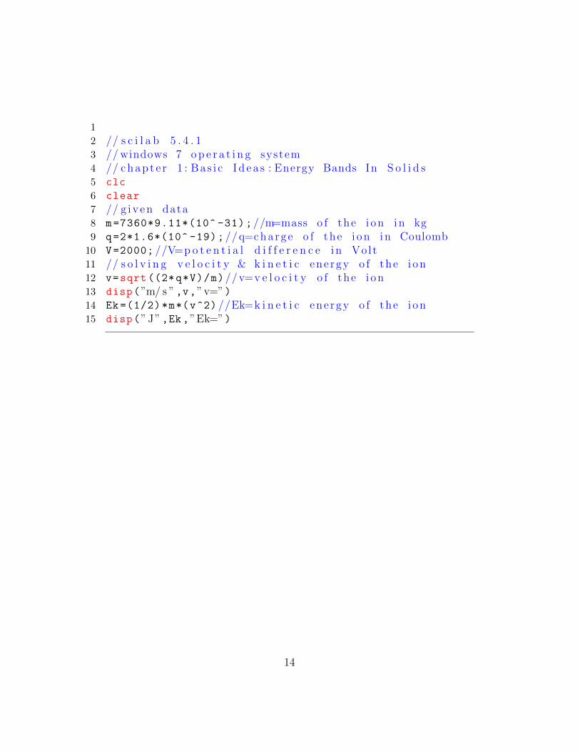
1
2 // s c i l a b 5 . 4 . 13 // windows 7 o p e r a t i n g system4 // c h a p t e r 1 : Ba s i c I d e a s : Energy Bands In S o l i d s5 clc
6 clear
7 // g i v e n data8 m=7360*9.11*(10^ -31);//m=mass o f the i on i n kg9 q=2*1.6*(10^ -19);//q=charge o f the i o n i n Coulomb10 V=2000; //V=p o t e n t i a l d i f f e r e n c e i n Vol t11 // s o l v i n g v e l o c i t y & k i n e t i c ene rgy o f the i o n12 v=sqrt ((2*q*V)/m)//v=v e l o c i t y o f the i o n13 disp(”m/ s ”,v,”v=”)14 Ek =(1/2)*m*(v^2) //Ek=k i n e t i c ene rgy o f the i on15 disp(”J”,Ek ,”Ek=”)
14

Chapter 2
Electron Emission from Solid
Scilab code Exa 2.7.1 to calculate the number of electrons emitted per unit area per second
1
2 // s c i l a b 5 . 4 . 13 // windows 7 o p e r a t i n g system4 // c h a p t e r 2 : E l e c t r o n Emis s ion from S o l i d s5 clc
6 clear
7 // g i v e n8 A=6.02*(10^5) //A=t h e r m i o n i c e m i s s i o n c o n s t a n t i n A(m
ˆ(−2) ) (Kˆ(−2) )9 Ew=4.54 //Ew=work f u n c t i o n i n eV
10 T=2500 //T=tempera tu r e i n Ke lv in11 kB =1.38*10^( -23) //kB=Boltzmann ’ s c o n s t a n t i n J/K12 e=1.6*10^( -19) // e=charge o f a n e l e c t r o n i n C13 b=(e*Ew)/kB //b=t h e r m i o n i c e m i s s i o n c o n s t a n t i n K14 disp(”K”,b,”b=”)15 Jx=A*(T^2)*exp(-b/T)// Jx=e m i s s i o n c u r r e n t d e n s i t y i n
A/mˆ ( 2 )16 disp(”A/(mˆ2) ”,Jx ,”Jx=”)17 n=Jx/e//n=number o f e l e c t r o n s emi t t ed per u n i t a r ea
per second i n (mˆ−2) ( s ˆ−1)18 disp(” (mˆ−2) ( s ˆ−1)”,n,”n=”)
15

Scilab code Exa 2.7.2 To find the percentage change in emission current
1
2 // s c i l a b 5 . 4 . 13 // windows 7 o p e r a t i n g system4 // c h a p t e r 2 : E l e c t r o n Emis s ion from S o l i d s5 clc
6 clear
7 // g i v e n8 T=2673 //T=tempera tu r e i n Ke lv in9 dT=10 //dT=change i n t empera tu r e i n Ke lv in10 Ew=4.54 //Ew=work f u n c t i o n i n eV11 e=1.6*10^( -19) // e=charge o f a n e l e c t r o n i n C12 kB =1.38*10^( -23) //kB=Boltzmann ’ s c o n s t a n t i n J/K13 // I =(S∗A∗ (Tˆ2) ) ∗ exp (−(( e ∗Ew) /(kB∗T) ) // I=e m i s s i o n
cu r r en t , S=s u r f a c e a r ea o f the f i l a m e n t , dI=changei n e m i s s i o n c u r r e n t
14 d=((2* dT)/T)+(((e*Ew)/(kB*(T^2))*dT))//d=change i ne m i s s i o n c u r r e n t
15 disp(””,d,”d=”)16 d*100 // p e r c e n t change i n e m i s s i o n c u r r e n t17 disp(”%”,d*100,”d∗100=”)
Scilab code Exa 2.7.3 difference between thermionic work function of the two emitters
1
2 // s c i l a b 5 . 4 . 13 // windows 7 o p e r a t i n g system4 // c h a p t e r 2 : E l e c t r o n Emis s ion from S o l i d s5 clc
6 clear
16
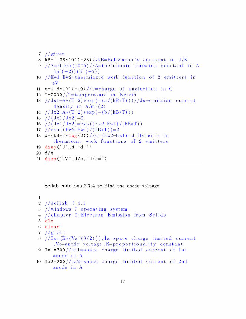
7 // g i v e n8 kB =1.38*10^( -23) //kB=Boltzmann ’ s c o n s t a n t i n J/K9 //A=6.02∗ (10ˆ5 ) //A=t h e r m i o n i c e m i s s i o n c o n s t a n t i n A
(mˆ(−2) ) (Kˆ(−2) )10 //Ew1 , Ew2=t h e r m i o n i c work f u n c t i o n o f 2 e m i t t e r s i n
eV11 e=1.6*10^( -19) // e=charge o f a n e l e c t r o n i n C12 T=2000 //T=tempera tu r e i n Ke lv in13 // Jx1=A∗ (Tˆ2) ∗ exp (−(a /(kB∗T) ) ) // Jx=e m i s s i o n c u r r e n t
d e n s i t y i n A/mˆ ( 2 )14 // Jx2=A∗ (Tˆ2) ∗ exp (−(b /(kB∗T) ) )15 // ( Jx1 / Jx2 )=216 // ( Jx1 / Jx2 )=exp ( ( Ew2−Ew1) /(kB∗T) )17 // exp ( ( Ew2−Ew1) /(kB∗T) )=218 d=(kB*T*log (2))//d=(Ew2−Ew1)=d i f f e r e n c e i n
t h e r m i o n i c work f u n c t i o n s o f 2 e m i t t e r s19 disp(”J”,d,”d=”)20 d/e
21 disp(”eV”,d/e,”d/ e=”)
Scilab code Exa 2.7.4 to find the anode voltage
1
2 // s c i l a b 5 . 4 . 13 // windows 7 o p e r a t i n g system4 // c h a p t e r 2 : E l e c t r o n Emis s ion from S o l i d s5 clc
6 clear
7 // g i v e n8 // Ia =(K∗ (Va ˆ ( 3 / 2 ) ) ) ; I a=space cha rge l i m i t e d c u r r e n t
,Va=anode v o l t a g e ,K=p r o p o r t i o n a l i t y c o n s t a n t9 Ia1 =300 // Ia1=space cha rge l i m i t e d c u r r e n t o f 1 s t
anode i n A10 Ia2 =200 // Ia2=space cha rge l i m i t e d c u r r e n t o f 2nd
anode i n A
17
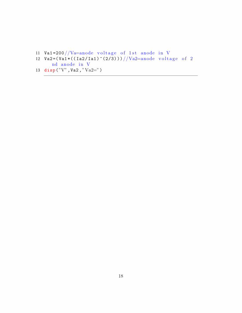
11 Va1 =200 //Va=anode v o l t a g e o f 1 s t anode i n V12 Va2=(Va1*((Ia2/Ia1)^(2/3)))//Va2=anode v o l t a g e o f 2
nd anode i n V13 disp(”V”,Va2 ,”Va2=”)
18

Chapter 3
PROPERTIES OFSEMICONDUCTORS
Scilab code Exa 3.11.1 To find the conductivity and resistivity
1
2 // s c i l a b 5 . 4 . 13 //WINDOWS 7 Operat ing System4 // c h a p t e r 3 PROPERTIES OF SEMICONDUCTORS5 // example 16
7 clc
8 // Given data9 T=300; //K
10 ni =1.5*10^16; // I n t r i n s i c c a r r i e r c o n c e n t a r t i o nper mˆ3
11 yn =0.13; // E l e c t r o n m o b i l i t y i n mˆ2/(V∗ s )12 yp =0.05; // Hole m o b i l i t y i n mˆ2/(V∗ s )13 e=1.6*10^ -19; // Charge o f e l e c t r o n i n C14
15 // Requ i red Formula16 Gi=e*ni*(yn+yp); // I n t r i n s i c c o n d u c t i v i t y17
18 Ri=1/Gi; // I n t r i n s i c r e s i s t i v i t y
19

19
20 disp( ’ S/m’ ,Gi , ’ I n t r i n s i c c o n d u c t i v i t y= ’ );21
22 disp( ’ ohm∗meter ’ ,Ri , ’ I n t r i n s i c r e s i s t i v i t y = ’ );23 //End
Scilab code Exa 3.11.2 To find Concentration of donor atoms
1
2 // s c i l a b 5 . 4 . 13 //WINDOWS 7 Operat ing Systems4 // c h a p t e r 3 PROPERTIES OF SEMICONDUCTORS5
6 // example 27 clc
8 // Given data9 Sn=480; // C o n d u c t i v i t y i n S/m
10 yn =0.38; // E l e c t r o n m o b i l i t y i n mˆ2/(V∗ s )11 e=1.6*10^ -19; // Charge o f e l e c t r o n i n C12
13 // Requ i red Formula14 Nd=Sn/(e*yn); // C o n c e n t r a t i o n o f donor atoms per m
ˆ315 disp( ’mˆ−3 ’ ,Nd , ’ C o n c e n t r a t i o n o f donor atoms ’ );16 //End
Scilab code Exa 3.11.4 To find intrinsic conductivity and resistance required
1
2 // s c i l a b 5 . 4 . 13 //OS−WINDOWS 74 // c h a p t e r 3 PROPERTIES OF SEMICONDUCTORS5 // example 4
20

6
7 clc
8 // Given data9 T=300; //K10 ni =1.5*10^16; // I n t r i n s i c c a r r i e r c o n c e n t a r t i o n
per mˆ311 yn =0.13; // E l e c t r o n m o b i l i t y i n mˆ2/(V∗ s )12 yp =0.05; // Hole m o b i l i t y i n mˆ2/(V∗ s )13 e=1.6*10^ -19; // Charge o f e l e c t r o n i n C14 l=0.01; // l e n g t h i n m15 a=10^ -6; // c r o s s s e c t i o n a l a r ea i n mˆ216
17 // Requ i red Formula18 Gi=e*ni*(yn+yp); // I n t r i n s i c c o n d u c t i v i t y19
20 Ri=l/(Gi*a); // Requ i red r e s i s t a n c e21
22 disp( ’ S/m’ ,Gi , ’ I n t r i n s i c c o n d u c t i v i t y= ’ );23
24 disp( ’ ohm ’ ,Ri , ’ r e q u i r e d r e s i s t a n c e ’ );25 //End
Scilab code Exa 3.11.5 To find the conductivity and current density of doped sample
1
2 // s c i l a b 5 . 4 . 13 // windows 7 o p e r a t i n g system4 // c h a p t e r 3 : P r o p e r t i e s o f Semiconduc to r s5 clc
6 clear
7 // g i v e n8 z=(100/60);// z=c o n d u c t i a r r i e r c o n c e n t r a t i o n i n /(m
ˆ3)9 ni =2.5*10^(19);// n i= i n t r i n s i c c o n d u c t i v i t y o f
i n t r i n s i c m a t e r i a l i n S/m
21

10 // (P/N) =(1/2) ; / / ( P/N)=r a t i o o f h o l e m o b i l i t y (P) toe l e c t r o n m o b i l i t y (N)
11 e=1.6*(10^ -19);// e=charge o f e l e c t r o n i n Coulomb12 N=(z/(e*ni *(1+(1/2))))
13 disp(” (mˆ2) /(V. s ) ”,N,”N=”)14 P=(N/2)
15 disp(” (mˆ2) /(V. s ) ”,P,”P=”)16 //Nd+p=Na+n ; n=e l e c t r o n c o n c e n t r a t i o n ; p=h o l e
c o n c e n t r a t i o n17 //np=( n i ˆ2)18 Nd =(10^20) //Nd=donor c o n c e n t r a t i o n i n /(mˆ3)19 Na =5*(10^19) //Na=a c c e p t o r c o n c e n t r a t i o n i n /(mˆ3)20 n=(1/2) *((Nd -Na)+sqrt (((Nd -Na)^2) +(4*( ni^2))))
21 disp(” /(mˆ3) ”,n,”n=”)22 p=(ni^2)/n
23 disp(” /(mˆ3) ”,p,”p=”)24 Z=e*((n*N)+(p*P))//Z=c o n d u c t i v i t y o f doped sample i n
S/m25 disp(”S/m”,Z,”Z=”)26 F=200 //F=a p p l i e d e l e c t r i c f i e l d i n V/cm27 J=Z*F// J=t o t a l c onduc t i on c u r r e n t d e n s i t y i n A/(mˆ2)28 disp(”A/(mˆ2) ”,J,”J=”)
Scilab code Exa 3.11.6 To find the electron and hole concentration and conductivity of doped sample
1
2 // s c i l a b 5 . 4 . 13 // windows 7 o p e r a t i n g system4 // c h a p t e r 3 : P r o p e r t i e s o f Semiconduc to r s5 clc
6 clear
7 // g i v e n8 ni =2.5*10^(19);// n i= i n t r i n s i c c o n d u c t i v i t y o f
i n t r i n s i c m a t e r i a l i n S/m9 Nd =5*(10^19) //Nd=donor c o n c e n t r a t i o n i n /(mˆ3)
22

10 n=(1/2) *(Nd+sqrt((Nd^2) +(4*(ni^2))))//n=e l e c t r o nc o n c e n t r a t i o n
11 disp(” /(mˆ3) ”,n,”n=”)12 p=(ni^2)/n//p=h o l e c o n c e n t r a t i o n13 disp(” /(mˆ3) ”,p,”p=”)14 N=0.38 //N=e l e c t r o n m o b i l i t y i n (mˆ2) /(V. s )15 P=0.18 //P=h o l e m o b i l i t y i n (mˆ2) /(V. s )16 e=1.6*(10^ -19) // e=e l e c t r o n i c cha rge i n Coulomb17 Z=e*((n*N)+(p*P))//Z=c o n d u c t i v i t y o f doped sample i n
S/m18 disp(”S/m”,Z,”Z=”)
Scilab code Exa 3.11.7 To find the required wavelength
1
2 // s c i l a b 5 . 4 . 13 // windows 8 o p e r a t i n g system4 // c h a p t e r 3 : P r o p e r t i e s o f Semiconduc to r s5 clc
6 clear
7 // g i v e n8 c=3*(10^8);// c=v e l o c i t y o f l i g h t i n vacuum i n m/ s9 h=6.6*(10^ -34);//h=Planck ’ s c o n s t a n t i n J . s
10 Eg =1.98*1.6*(10^ -19) //Eg=band gap i n J11 // c a l c u l a t i n g Y=r e q u i r e d wave l ength12 Y=((c*h)/Eg)/(10^ -9)
13 disp(”nm”,Y,”Y=”)
Scilab code Exa 3.11.8 To find the magnetic and hall field
1
2 // s c i l a b 5 . 4 . 13 // windows 7 o p e r a t i n g system
23

4 // c h a p t e r 3 : P r o p e r t i e s o f Semiconduc to r s5 clc
6 clear
7 // g i v e n8 RH=(10^ -2);//RH=H a l l c o e f f i c i e n t i n (mˆ3) /C9 VH=(10^ -3);//VH=H a l l Vo l tage i n V10 b=2*(10^ -3);//b=width i n m11 I=(10^ -3);// I=c u r r e n t i n A12 //RH=(VH∗b ) /( I ∗B)13 B=(VH*b)/(I*RH)//B=magnet i c f i e l d14 disp(”T”,B,”B=”)15 t=(10^ -3) // t=t h i c k n e s s i n m16 FH=(VH/t)//FH=H a l l f i e l d17 disp(”V/m”,FH ,”FH=”)
24

Chapter 4
Metal Semiconductor Contacts
Scilab code Exa 4.7.1 to find barrier height and depletion region width and maximum electric field
1
2 // s c i l a b 5 . 4 . 13 // windows 7 o p e r a t i n g system4 // c h a p t e r 4 : Metal−Semiconductor Contact s5 clc
6 clear
7 // g i v e n8 Qm=4.55 //Qm=work f u n c t i o n o f t u n g s t e n i n eV9 X=4.01 //X=e l e c t r o n a f f i n i t y o f s i l i c o n i n eV10 eQb=(Qm -X)//eQb=b a r r i e r h e i g h t as s e en from the
meta l11 disp(”eV”,eQb ,”eQb=”)12 a=0.21 // a=(Ec−Ef )=f o r b i d d e n gap i n eV13 eVbi=eQb -a// eVbi=b a r r i e r h e i g h t from semi conduc to r
s i d e14 disp(”eV”,eVbi ,” eVbi=”)15 Es =11.7*8.854*(10^ -12) // Es=p e r m i t t i v i t y o f
s em i conduc to r ; 11 . 7= d i e l e c t r i c c o n s t a n t o f s i l i c o n16 e=1.6*10^( -19) // e=charge o f an e l e c t r o n17 Nd =10^22 //Nd=donor c o n c e n t r a t i o n i n mˆ−318 W=((2* Es*eVbi)/(e*Nd))^(1/2) //W=width o f the
25
d e p l e t i o n r e g i o n19 disp(”m”,W,”W=”)20 Fm=((e*Nd*W)/Es)//Fm=maximum e l e c t r i c f i e l d i n V/m21 disp(”V/m”,Fm ,”Fm=”)
Scilab code Exa 4.7.2 to find the barrier height and concentration
1
2 // s c i l a b 5 . 4 . 13 // windows 7 o p e r a t i n g system4 // c h a p t e r 4 : Metal−Semiconductor Contact s5 clc
6 clear
7 // g i v e n8 // as per g i v e n data b a r r i e r h e i g h t =Vbi=i n t e r c e p t
on Vr a x i s =0.4 V9 Es =11.7*8.854*(10^ -12) // Es=p e r m i t t i v i t y o f
s em i conduc to r ; 11 . 7= d i e l e c t r i c c o n s t a n t o f s i l i c o n10 e=1.6*10^( -19) // e=charge o f an e l e c t r o n11 m=4.4*10^(15) //m=s l o p e o f (1/Cˆ2) vs Vr p l o t o f a
Schot tky c o n t a c t i n (cmˆ4) (Fˆ−2) (Vˆ−1)12 //m=2/( e∗Es∗Nd)13 Nd =(2*10^8) /(e*Es*m)//Nd=donor c o n c e n t r a t i o n i n
s i l i c o n i n mˆ−314 disp(”mˆ−3”,Nd ,”Nd=”)
Scilab code Exa 4.7.3 to calculate barrier lowering and the position of the maximum barrier height
1
2 // s c i l a b 5 . 4 . 13 // windows 7 o p e r a t i n g system4 // c h a p t e r 4 : Metal−Semiconductor Contact s5 clc
26
6 clear
7 // g i v e n8 e=1.6*10^ -19 // e=charge o f an e l e c t r o n i n C9 Fa =7*10^6 //Fa=r e v e r s e b i a s f i e l d i n V/m10 Es =13.1*8.854*10^ -12 // ( Es/Eo ) =13 . 1 ; Eo=8.854∗10ˆ−1211 dQ=((e*Fa)/(4* %pi*Es))^(1/2) //dQ=b a r r i e r l o w e r i n g i n
V12 disp(”V”,dQ ,”dQ=”)13 Xm=(dQ)/(2*Fa)//Xm=p o s i t i o n o f the maximum b a r r i e r
h e i g h t14 disp(”m”,Xm ,”Xm=”)
Scilab code Exa 4.7.4 to determine the effective richardson constant
1
2 // s c i l a b 5 . 4 . 13 // windows 7 o p e r a t i n g system4 // c h a p t e r 4 : Metal−Semiconductor Contact s5 clc
6 clear
7 // g i v e n8 // Js=A∗ (Tˆ2) ∗ exp (−(( e ∗Qbn) /(kB∗T) ) )9 kB =1.38*10^( -23) //kB=Boltzmann ’ s c o n s t a n t i n J/K10 T=300 //T=tempera tu r e i n Ke lv in11 e=1.6*10^ -19 // e=charge o f an e l e c t r o n i n C12 Js=6*10^ -5 // Js=e m i s s i o n c u r r e n t d e n s i t y i n A/cmˆ213 Qbn =0.668 //Qbn=b a r r i e r h e i g h t i n V14 A=(Js/(T^2))*exp((e*Qbn)/(kB*T))//A=Richardson
c o n s t a n t15 disp(” (cmˆ−2) (Kˆ−2)”,A,”A=”)
Scilab code Exa 4.7.5 to calculate current in a Schottky diode
27

1
2 // s c i l a b 5 . 4 . 13 // windows 7 o p e r a t i n g system4 // c h a p t e r 4 : Metal−Semiconductor Contact s5 clc
6 clear
7 // g i v e n8 e=1.6*10^ -19 // e=charge o f an e l e c t r o n i n C9 V=0.32 //V =a p p l i e d fo rward b i a s i n V10 kB =1.38*10^( -23) //kB=Boltzmann ’ s c o n s t a n t i n J/K11 T=300 //T=Temperature i n Ke lv in12 Js=0.61 // Js=r e v e r s e s a t u r a t i o n c u r r e n t d e n s i t y i n A/
mˆ213 J=Js*(exp((e*V)/(kB*T)) -1) // J=c u r r e n t d e n s i t y i n A/m
ˆ214 disp(”A/mˆ2 ”,J,”J=”)15 A=4*10^ -8 //A=c r o s s s e c t i o n a l a r ea i n mˆ216 I=(J*A)*10^3 // I=c u r r e n t17 disp(”mA”,I,” I=”)
28
Chapter 5
Semiconductor Junction Diodes
Scilab code Exa 5.7.1 To find the voltage to be applied across the junction
1
2 // s c i l a b 5 . 4 . 13 // windows 7 o p e r a t i n g system4 // Chapter 5 : Semiconductor J un c t i on Diodes5 clc
6 clear
7 // I=I s ∗ ( exp ( ( e ∗V) /kB∗T)−1)8 I=50*10^( -3) // I=Forward c u r r e n t i n ampere9 Is=5*10^( -6) // I s=Rever s e s a t u r a t i o n c u r r e n t i n
ampere10 e=1.6*10^( -19) // e=charge o f e l e c t r o n i n coulomb11 //V=v o l t a g e12 kB =1.38*10^( -23) //kB=Boltzmann ’ s c o n s t a n t i n J o u l e /
k e l v i n13 T=300 //T=Temperature i n k e l v i n14 a=(I/Is)+1
15 // exp ( ( e∗V) /kB∗T)=a16 V=((kB*T)/e)*log (10^4)
17 disp(”V”,V,”V=”)
29

Scilab code Exa 5.7.2 To calculate the ratio of current for forward bias to that of reverse bias
1
2 // s c i l a b 5 . 4 . 13 // windows 7 o p e r a t i n g system4 // c h a p t e r 5 : Semiconductor J un c t i on Diodes5 clc
6 clear
7 // g i v e n8 e=1.6*10^ -19 // e=charge o f an e l e c t r o n i n C9 V1=0.06 //V1=a p p l i e d fo rward b i a s i n V
10 V2=( -0.06) //V2 =a p p l i e d r e v e r s e b i a s i n V11 kB =1.38*10^( -23) //kB=Boltzmann ’ s c o n s t a n t i n J/K12 T=300 //T=Temperature i n Ke lv in13 // I s=r e v e r s e s a t u r a t i o n c u r r e n t i n A14 // I1=I s ∗ ( exp ( ( e∗V1) /(kB∗T) )−1)// I1=c u r r e n t f o r
f o rward b i a s15 // I2=I s ∗ ( exp ( ( e∗V2) /(kB∗T) )−1)// I2=c u r r e n t f o r
r e v e r s e b i a s16 a=((exp((e*V1)/(kB*T)) -1))/((exp((e*V2)/(kB*T)) -1))
// a=( I1 / I2 )17 disp(””,abs(a),”a”)
Scilab code Exa 5.7.3 To determine the static and dynamic resistance of the diode
1
2 // s c i l a b 5 . 4 . 13 // windows 7 o p e r a t i n g system4 // Chapter 5 : Semiconductor J un c t i on Diodes5 clc
6 clear
7 V=0.9 //V=forward b i a s v o l t a g e
30

8 I=60*10^( -3) // I=Current i n ampere9 rdc=(V/I)// rdc=s t a t i c r e s i s t a n c e i n ohm10 n=2 //n=e m i s s i o n c o e f f i c i e n t11 rac =((26*n*10^( -3))/I)// r a c=dynamic r e s i s t a n c e12 disp(”ohm”,rdc ,” rdc=”)13 disp(”ohm”,rac ,” ra c=”)
Scilab code Exa 5.7.4 To calculate the increase in the bias voltage
1
2 // s c i l a b 5 . 4 . 13 // windows 7 o p e r a t i n g system4 // c h a p t e r 5 : Semiconductor J un c t i on Diodes5 clc
6 clear
7 e=1.6*10^( -19) // e=charge o f an e l e c t r o n i n C8 kB =1.38*10^( -23) //kB=Boltzmann ’ s c o n s t a n t i n J/K9 //V, V1=forward b i a s v o l t a g e s i n V10 n=2 //n=e m i s s i o n c o e f f i c i e n t f o r s i l i c o n pn j u n c t i o n
d i ode11 T=300 //T=Temperature i n k e l v i n12 // I s=Rever s e s a t u r a t i o n c u r r e n t i n A13 // I=I s ∗ ( exp ( ( e ∗V) /( n∗kB∗T) ) ) // I=c u r r e n t f o r f o rward
b i a s v o l t a g e V14 // 2 I=I s ∗ ( exp ( ( e∗V1) /( n∗kB∗T) ) ) //2 I=c u r r e n t f o r
f o rward b i a s v o l t a g e V115 // exp ( ( e ∗ (V1−V) /( n∗kB∗T) ) )=216 a=(((n*kB*T)/e)*log(2))*10^3 // a=(V1−V)=i n c r e a s e i n
the b i a s v o l t a g e i n V17 disp(”mV”,a,”V1−V”)
Scilab code Exa 5.7.5 To find the bias voltage of pn junction diode
31

1
2 // s c i l a b 5 . 4 . 13 // windows 7 o p e r a t i n g system4 // c h a p t e r 5 : Semiconductor J un c t i on Diodes5 clc
6 clear
7 e=1.6*10^( -19) // e=charge o f an e l e c t r o n i n C8 kB =1.38*10^( -23) //kB=Boltzmann ’ s c o n s t a n t i n J/K9 n=2 //n=e m i s s i o n c o e f f i c i e n t f o r s i l i c o n pn j u n c t i o n
d i ode10 T=300 //T=Temperature i n k e l v i n11 // I s=Rever s e s a t u r a t i o n c u r r e n t i n A12 //V=b i a s v o l t a g e i n V13 // I=I s ∗ ( exp ( ( e ∗V) /( n∗kB∗T) )−1)// I=r e v e r s e c u r r e n t i n
A14 // I =(−( I s /2) )15 a=(((n*kB*T)/e)*log (1/2))*10^3 // a=b i a s f o r r e v e r s e
c u r r e n t i n s i l i c o n pn j u n c t i o n d i ode16 disp(”mV”,a,”V”)17 disp(”The n e g a t i v e s i g n s u g g e s t s d i ode i n r e v e r s e
b i a s ”)
Scilab code Exa 5.7.6 To calculate the rise in temperature
1
2 // s c i l a b 5 . 4 . 13 // windows 7 o p e r a t i n g system4 // c h a p t e r 5 : Semiconductor J un c t i on Diodes5 clc
6 clear
7 //T1 , T2=Temperature i n k e l v i n8 // I s 1=Rever s e s a t u r a t i o n c u r r e n t at t empera tu r e T1
i n ampere9 // I s 2=Rever s e s a t u r a t i o n c u r r e n t at t empera tu r e T2
i n ampere
32

10 // I s 2=I s 1 ∗2 ˆ ( ( T2−T1) /10)11 // ( ( T2−T1) /10) ∗ l o g ( 2 )=l o g ( I s 2 / I s 1 )12 //b=( I s 2 / I s 1 )13 b=50
14 a=((10* log(b))/log(2))// a=(T2−T1)=r i s e i nt empera tu re i n d e g r e e c e l c i u s
15 disp(”C”,a,”T2−T1”)
Scilab code Exa 5.7.7 To calculate the maximum permissible battery voltage
1
2 // s c i l a b 5 . 4 . 13 // windows 7 o p e r a t i n g system4 // c h a p t e r 5 : Semiconductor J un c t i on Diodes5 clc
6 clear
7 V=0.6 //V=c u t i n v o l t a g e i n V8 r=150 // r=fo rward r e s i s t a n c e i n ohm9 P=200*(10^ -3) //P=maximum power i n Watt10 //P=( i ˆ2) ∗ r where i=maximum s a f e d i ode c u r r e n t11 i=(sqrt(P/r))*10^3
12 disp(”mA”,i,” i=”)13 // i =((Vb/3)−V) /3 by a p p l y i n g KCL14 Vb=((3*i)+V)*3 //Vb=maximum p e r m i s s i b l e b a t t e r y
v o l t a g e15 disp(”V”,Vb ,”Vb=”)
Scilab code Exa 5.7.8 To calculate series resistance and the range over which load resistance can be varied
1
2 // s c i l a b 5 . 4 . 13 // windows 7 o p e r a t i n g system4 // c h a p t e r 5 : Semiconductor J un c t i on Diodes
33

5 clc
6 clear
7 V=15 //V=supp ly v o l t a g e8 Vz=12 //Vz=Zener v o l t a g e9 P=0.36 //P=power o f Zener d i ode
10 //P=Vz∗ I11 I=(P/Vz)// I=maximum a l l o w a b l e Zener c u r r e n t12 disp(”A”,I,” I=”)13 Vr=V-Vz //Vr=v o l t a g e drop a c r o s s s e r i e s r e s i s t a n c e R14 disp(”V”,Vr ,”Vr=”)15 R=Vr/I//R=s e r i e s r e s i s t a n c e16 disp(”ohm”,R,”R=”)17 // I=I z+I l18 Iz=2*(10^ -3) // I z=minimum d iode c u r r e n t19 Il=I-Iz // I l=c u r r e n t through l oad r e s i s t a n c e Rl20 disp(”A”,Il ,” I l=”)21 Rlm=Vz/Il //Rlm=minimum v a l u e o f Rl22 disp(”ohm”,Rlm ,”Rlm=”)23 disp(”The a l l o w a b l e range o f v a r i a t i o n o f Rl i s
4 2 8 . 6 ohm<=Rl< i n f i n i t e ”)
Scilab code Exa 5.7.9 To determine the limits between which the supply voltage can vary
1
2 // s c i l a b 5 . 4 . 13 // windows 7 o p e r a t i n g system4 // c h a p t e r 5 : Semiconductor J un c t i on Diodes5 clc
6 clear
7 V=15 //V=supp ly v o l t a g e8 Vz=12 //Vz=Zener v o l t a g e9 P=0.36 //P=power o f Zener d i ode
10 //P=Vz∗ I11 I=(P/Vz)// I=maximum a l l o w a b l e Zener c u r r e n t12 disp(”A”,I,” I=”)
34

13 Iz=2*10^( -3) // I z=minimum v a l u e a t t a i n e d by the z e n e rc u r r e n t
14 Rl=1000 // Rl=load r e s i s t a n c e15 i=Vz/Rl // i=load c u r r e n t16 disp(”A”,i,” i=”)17 Imin=Iz+i// Imin=minimum a l l o w a b l e v a l u e o f c u r r e n t18 R=100 //R=s e r i e s r e s i s t a n c e19 Vr=Imin*R//Vr=v o l t a g e drop a c r o s s R20 disp(”V”,Vr ,”Vr=”)21 Vmin=Vz+Vr //Vmin=minimum v a l u e o f V22 disp(”V”,Vmin ,”Vmin=”)23 I1=I+i
24 disp(”A”,I1 ,” I1=”)25 VR=I1*R
26 disp(”V”,VR ,”VR=”)27 Vmax=Vz+VR //Vmax=maximum v a l u e o f V28 disp(”V”,Vmax ,”Vmax=”)29 disp(”V can vary between Vmin & Vmax”)
Scilab code Exa 5.7.10 To find whether power dissipated exceeds the maximum power limit
1
2 // s c i l a b 5 . 4 . 13 // windows 7 o p e r a t i n g system4 // c h a p t e r 5 : Semiconductor J un c t i on Diodes5 clc
6 clear
7 Vz=3 //Vz=breakdown v o l t a g e o f z e n e r d i ode8 Vi=12 // Vi=input v o l t a g e9 V=[12; -3] //V=[ Vi :−Vz ]
10 R1=1000
11 R2=1000
12 R3=500 //R1 , R2 , R3=r e s i s t a n c e s13 R=[R1+R2 -R2;-R2 R2+R3]
14 I1=inv(R)*V// s o l v i n g t h i s matr ix on the b a s i s o f
35
a p p l i c a t i o n o f KCL & KVL, we g e t the v a l u e s o fbranch c u r r e n t s I & I z as I1 =[ I ; I z ]
15 disp(”A”,I1(1),” I=”)16 disp(”A”,I1(2),” I z=”)17 Pz=Vz*I1(2) //Pz=power d i s s i p a t e d i n z e n e r d i ode18 disp(”W”,Pz ,”Pz=”)19 disp(”Power d i s s i p a t e d does not exceed the maximum
power l i m i t o f 20mW”)
Scilab code Exa 5.7.11 To determine the range of variation of the output voltage
1
2 // s c i l a b 5 . 4 . 13 // windows 7 o p e r a t i n g system4 // c h a p t e r 5 : Semiconductor J un c t i on Diodes5 clc
6 clear
7 Vs1 =15
8 Vs2 =30 //Vs=supp ly v o l t a g e v a r y i n g from 15( Vs1 ) to30( Vs2 ) Vol t
9 Vzo=9 //Vzo=knee v o l t a g e10 rZ=5 // rZ=dynamic r e s i s t a n c e i n ohms11 R=800 //R=s e r i e s r e s i s t a n c e i n ohms12 Izmin=(Vs1 -Vzo)/(R+rZ)// Izmin=c u r r e n t through z e n e r
d i ode when Vs i s 15 V13 disp(”A”,Izmin ,” Izmin=”)14 Vomin=(rZ*Izmin)+Vzo //Vomin=c o r r e s p o n d i n g minimum
output v o l t a g e15 disp(”V”,Vomin ,”Vomin=”)16 Izmax=(Vs2 -Vzo)/(R+rZ)// Izmax=c u r r e n t through z e n e r
d i ode when Vs i s 30 V17 disp(”A”,Izmax ,” Izmax=”)18 Vomax=(rZ*Izmax)+Vzo //Vomax=c o r r e s p o n d i n g maximum
output v o l t a g e19 disp(”V”,Vomax ,”Vomax=”)
36
20 disp(” Output v o l t a g e Vo v a r i e s i n the range Vomin toVomax”)
Scilab code Exa 5.7.12 To find the value of resistance R
1
2 // s c i l a b 5 . 4 . 13 // windows 7 o p e r a t i n g system4 // c h a p t e r 5 : Semiconductor J un c t i on Diodes5 clc
6 clear
7 V=35 //V=supp ly v o l t a g e8 Iz =25*10^( -3) // I z=d iode c u r r e n t9 Il=5*10^( -3) // I l=load c u r r e n t
10 Vzo=7 //Vzo=knee v o l t a g e o f z e n e r d i ode11 rZ=6 // rZ=dynamic r e s i s t a n c e i n ohms12 Vz=Vzo+(rZ*Iz)//Vz=z e n e r v o l t a g e13 disp(”V”,Vz ,”Vz=”)14 I=Iz+Il // I=c u r r e n t through r e s i s t a n c e R15 disp(”A”,I,” I=”)16 R=(V-Vz)/I
17 disp(”ohm”,R,”R=”)
37

Chapter 6
Diode Circuits
Scilab code Exa 6.11.1 To find various currents voltages power conversion efficiency and percentage regulation
1
2 // s c i l a b 5 . 4 . 13 // windows 7 o p e r a t i n g system4 // c h a p t e r 6 : Diode C i r c u i t s5 clc;
6 clear;
7 // g i v e n data8 Vrms =20; // i n v o l t s9 Vm =20*1.41; // i n v o l t s
10 Rf=50; // fo rward r e s i s t a n c e i n ohms11 RL =1200; // l oad r e s i s t a n c e i n ohms12
13 Im=Vm/(Rf+RL); // peak l oad c u r r e n t14 format(”v” ,7)15 disp( ’A ’ ,Im , ’ Im= ’ );16
17 Idc=Im/%pi; // dc l oad c u r r e n t18 format(”v” ,8) // to s e t the c u r r e n t p r i n t i n g format
with the s p e c i f i e d parameter type19 disp( ’A ’ ,Idc , ’ I d c= ’ );20
38

21 Irms=Im/2; // rms l oad c u r r e n t22 Irms1=sqrt((Irms ^2) -(Idc^2))// rms ac l oad c u r r e n t23 format(”v” ,8)24 disp( ’A ’ ,Irms1 , ’ rms ac l oad c u r r e n t i s= ’ );25
26 Vdc=Idc*Rf; //Dc v o l t a g e a c r o s s the d i ode27 format(”v” ,6)28 disp( ’V ’ ,Vdc , ’Dc v o l t a g e a c r o s s the d i ode= ’ );29
30 Pdc=Idc*Idc*RL; //Dc output power31 format(”v” ,6)32 disp( ’W’ ,Pdc , ’Dc output power= ’ );33
34 n=40.6/(1+( Rf/RL)); // c o n v e r s i o n e f f i c i e n c y35 format(”v” ,5)36 disp( ’% ’ ,n, ’ c o n v e r s i o n e f f i c i e n c y= ’ );37
38 s=Rf*100/RL; // P e r t c e n t a g e r e g u l a t i o n39 format(”v” ,5)40 disp( ’% ’ ,s, ’ P e r t c e n t a g e r e g u l a t i o n= ’ );41
42 // end
Scilab code Exa 6.11.2 To find various currents power ripple voltage percentage regulation and effiiciency of rectification
1
2 // s c i l a b 5 . 4 . 13 // windows 7 o p e r a t i n g system4 // c h a p t e r 6 : Diode C i r c u i t s5 clc;
6 clear;
7 // g i v e n data8 Rf=100; // fo rward r e s i s t a n c e i n ohms9 Rl =1000; // l oad r e s i s t a n c e i n ohms
10 n=10; // Primary to s e condary t u r n s r a t i o
39

11 Vp=240; // Primary input V( rms )12
13 Vm =24*(2^(1/2))/2; // s e condary peak v o l t a g e fromc e n r e tap
14 Vs=Vp/n; // Secondary input v o l t a g e15 Im=Vm/(Rf+Rl); // peak c u r r e n t through the
r e s i s t a n c e i n A16 Idc =(2*Im)/%pi; //DC Load c u r r e n t i n A17 format(”v” ,8)18 disp( ’A ’ ,Idc , ’DC load c u r r e n t Idc= ’ ,);19 I=Idc/2; // D i r e c t c u r r e n t s u p p l i e d by each d i ode
i n A20 format(”v” ,7)21 disp( ’A ’ ,I, ’ D i r e c t c u r r e n t s u p p l i e d by each d i ode
Idc= ’ ,);22 Pdc=Idc*Idc*Rl; //DC power output23 format(”v” ,6)24 disp( ’W’ ,Pdc , ’ Pdc= ’ );25 Irms=Im /(2^(1/2));
26 Vrp=sqrt((Irms*Irms) -(Idc*Idc))*Rl; // Ripp l ev o l t a g e i n V
27 format(”v” ,7)28 disp( ’V ’ ,Vrp , ’ R ipp l e v o l t a g e Vrp= ’ );29
30
31 M=(Rf *100)/Rl; // p e r c e n t a g e r e g u l a t i o n32 disp( ’% ’ ,M, ’ Pe r c en tage r e g u l a t i o n= ’ );33 n=81.2/(1+( Rf/Rl)); // E f f i c i e n c y o f r e c t i f i c a t i o n34 format(”v” ,5)35 disp( ’% ’ ,n, ’ E f f i c i e n c y o f r e c t i f i c a t i o n ’ );36
37 // end
Scilab code Exa 6.11.3 To calculate the dc load voltage ripple voltage and the percentage regulation
40

1
2 // s c i l a b 5 . 4 . 13 // windows 7 o p e r a t i n g system4 // c h a p t e r 6 : Diode C i r c u i t s5 clc;
6 clear;
7 // g i v e n data8 Rf=50; // fo rward r e s i s t a n c e i n ohms9 Rl =2500; // l oad r e s i s t a n c e i n ohms10 Vp=30; // Primary input V( rms )11 Vm=30* sqrt (2);
12
13 Im=Vm/(2*Rf+Rl); // peak l oad c u r r e n t i n A14 Idc =2*Im/%pi;
15
16 Vdc=Idc*Rl; //DC load v o l t a g e17 disp( ’V ’ ,Vdc , ’ Vdc= ’ );18 Irms=Im/sqrt (2);
19 Vrp=Rl*sqrt ((( Irms*Irms)-(Idc*Idc))); // Ripp l ev o l t a g e i n V
20 disp( ’V ’ ,Vrp , ’ R ipp l e v o l t a g e Vrp= ’ );21
22 M=(2*Rf/Rl)*100; // Pe r c en tage r e g u l a t i o n23 disp( ’% ’ ,M, ’ Pe r c en tage r e g u l a t i o n= ’ );24
25 // end
Scilab code Exa 6.11.4 To calculate ripple voltage and the percentage ripple
1
2 // s c i l a b 5 . 4 . 13 // windows 7 o p e r a t i n g system4 // c h a p t e r 6 : Diode C i r c u i t s5 clc;
6 clear;
41
7 // g i v e n data8
9 Vdc =20; //DC v a l u e i n V10 Vpp =1; // Peak to peak r i p p l e v o l t a g e i n V11
12 Vp=Vpp/2; // Peak r i p p l e v o l t a g e i n V13 Vrms=Vp/sqrt (2); //Vrms v o l t a g e i n V14 S=Vrms/Vdc; // Ripp l e Facto r15 format(”v” ,7)16 disp(S, ’ R ipp l e f a c t o r= ’ )17 T=S*100;
18 format(”v” ,5)19 disp(”%”,T, ’ Pe r c en tage R ipp l e= ’ )20 // end
Scilab code Exa 6.11.5 To design a full wave rectifier with L type LC filter
1 // s c i l a b 5 . 4 . 12 //Windows 7 o p e r a t i n g system3 // c h a p t e r 6 Diode C i r c u i t s4 clc
5 clear
6 // For a f u l l wave r e c t i f i e r7 //L−type LC f i l t e r8 f=50 // f=l i n e f r e q u e n c y i n Hz9 w=2*%pi*f
10 Vdc =10 //Vdc=dc output v o l t a g e11 Idc =100*10^ -3 // Idc=load c u r r e n t i n Amperes12 y=0.02 //y=a l l o w a b l e r i p p l e f a c t o r13 //y=s q r t ( 2 ) / ( 1 2∗ (wˆ2) ∗L∗C)14 // Let L∗C=a . . . . . . . . . . . . . . . ( 1 )15 a=sqrt (2)/(y*12*(w^2))
16 RL=Vdc/Idc //RL=load r e s i s t a n c e17 // Lc= c r i t i c a l i n d u c t a n c e18 // Lc=RL/(3∗w)
42
19 // For l i n e f r e q u e n c y o f 50Hz , Lc=RL/(300∗%pi )20 // Lc=RL/95021 Lc=RL/950
22 format(”v” ,4)23 L=0.1 // Assumed i n d u c t a n c e i n henry24 C=a/L//C=c a p a c i t a n c e c a l c u l a t e d from e q u a t i o n ( 1 )25 format(”v” ,4)26 L1=1 // Assumed i n d u c t a n c e i n henry27 C1=a/L1 //C1=c a p a c i t a n c e c a l c u l a t e d from e q u a t i o n ( 1 )28 format(”v” ,4)29 Rb=950*L1 //Rb=b l e e d e r r e s i s t a n c e f o r good v o l t a g e
r e g u l a t i o n30 disp(”The d e s i g n e d v a l u e s o f the components f o r a
f u l l wave r e c t i f i e r with L−type LC f i l t e r a r e ”)31 disp(”ohm”,RL ,”The l oad r e s i s t a n c e RL i s =”)32 disp(”H”,Lc ,”The c r i t i c a l i n d u c t a n c e Lc i s =”)33 disp(”H”,L,”The i n d u c t a n c e L i s=”)34 disp(” F ”,C/10^-6,”The c a p a c i t a n c e C i s ”)//C i s
c o n v e r t e d i n terms o f m i c r o f a r a d35 // In t ex tbook 957 F i s approx imate l y taken as 600
F36 disp(”H”,L1 ,”But i f the i n d u c t a n c e L d e s i g n e d i s o f
the v a l u e =”)37 disp(” F ”,C1/10^-6,” the c a p a c i t a n c e C w i l l be o f
the v a l u e =”)//C1 i s c o n v e r t e d i n terms o fm i c r o f a r a d
38 disp(”So , a s tandard v a l u e o f 50 F can be used i np r a c t i c e ”)
39 disp(”ohm”,Rb ,”The b l e e d e r r e s i s t a n c e Rb f o r goodv o l t a g e r e g u l a t i o n i s=”)
40 disp(”As Rb i s much g r e a t e r than RL, l i t t l e power i swasted i n Rb . This r e f l e c t s the advantage o fs e l e c t i n g L>Lc”)
43

Chapter 7
Junction TransistorCharacteristics
Scilab code Exa 7.13.1 To find the voltage gain and power gain of a transistor
1
2 // s c i l a b 5 . 4 . 13 // windows 7 o p e r a t i n g system4 // c h a p t e r 7 : Ju nc t i on T r a n s i s t o r C h a r a c t e r i s t i c s5 clc;
6 clear;
7 // g i v e n data8 a=0.99; // a=f r a c t i o n o f the e m i t t e r c u r r e n t
c o n t r i b u t e d by the c a r r i e r s i n j e c t e d i n t o thebase and r e a c h i n g the c o l l e c t o r
9 Rl =4500; // Load r e s i s t a n c e i n ohms10 rd=50; // dynamic r e s i s t a n c e i n ohms11
12 Av=a*Rl/rd; // Vo l tage ga in13 Ap=a*Av;// Power ga in14
15 disp(Av, ’Av= ’ );16 disp(Ap, ’Ap= ’ );
44

Scilab code Exa 7.13.2 To find the base and collector current of a given transistor
1
2 // s c i l a b 5 . 4 . 13 // windows 7 o p e r a t i n g system4 // c h a p t e r 7 : Ju nc t i on T r a n s i s t o r C h a r a c t e r i s t i c s5 clc;
6 clear;
7 // g i v e n data8 a=0.98; // a=f r a c t i o n o f the e m i t t e r c u r r e n t
c o n t r i b u t e d by the c a r r i e r s i n j e c t e d i n t o thebase and r e a c h i n g the c o l l e c t o r
9 Ie =0.003; // e m i t t e r c u r r e n t i n A10 Ico =10*10^ -6; // r e v e r s e s a t u r a t i o n c u r r e n t i n A11
12 Ic=a*Ie+Ico; // c o l l e c t o r c u r r e n t i n A13 format(”v” ,8)14 disp( ’mA’ ,Ic/10^-3, ’ I c= ’ );// I c i s c o n v e r t e d i n terms
o f mA15
16 Ib=Ie-Ic; // base c u r r e n t i n A17 format(”v” ,8)18 disp( ’ A ’ ,Ib/10^-6, ’ Ib= ’ );// Ib i s c o n v e r t e d i n
terms o f A
Scilab code Exa 7.13.3 To calculate the emitter and collector current of a given transistor
1
2 // s c i l a b 5 . 4 . 13 // windows 7 o p e r a t i n g system4 // c h a p t e r 7 : Ju nc t i on T r a n s i s t o r C h a r a c t e r i s t i c s5 clc;
45
6 clear;
7 // g i v e n data8 a=0.975; // a=f r a c t i o n o f the e m i t t e r c u r r e n t
c o n t r i b u t e d by the c a r r i e r s i n j e c t e d i n t o thebase and r e a c h i n g the c o l l e c t o r
9 Ico =10*10^ -6; // r e v e r s e s a t u r a t i o n c u r r e n t i n A10 Ib =250*10^ -6; // base c u r r e n t i n A11
12 b=a/(1-a); // t r a n s i s t o r ga in13 disp(b, ’ g a i n B= ’ );14 Ic=b*Ib+(b+1)*Ico; // c o l l e c t o r c u r r e n t i n A15 format(”v” ,5)16 disp( ’mA’ ,Ic/10^-3, ’ I c= ’ );// I c i s c o n v e r t e d i n terms
o f mA17 Ie=(Ic-Ico)/a; // e m i t t e r c u r r e n t i n A18 format(”v” ,5)19 disp( ’mA’ ,Ie/10^-3, ’ I e= ’ );// I e i s c o n v e r t e d i n terms
o f mA
Scilab code Exa 7.13.4 To calculate the voltage between collector and emitter terminals
1
2 // s c i l a b 5 . 4 . 13 // windows 7 o p e r a t i n g system4 // c h a p t e r 7 : Ju nc t i on T r a n s i s t o r C h a r a c t e r i s t i c s5 clc;
6 clear;
7 // g i v e n data8 b=125; //b=forward c u r r e n t t r a n s f e r r a t i o or dc
c u r r e n t ga in9 Vbe =0.6; // base to e m i t t e r v o l t a g e i n V
10
11 Ib=(10-Vbe)/(310*10^3); // base c u r r e n t i n A12 disp( ’mA’ ,Ib*10^3, ’ Ib= ’ );13 Ic=b*Ib; // c o l l e c t o r c u r r e n t i n A
46

14 disp( ’mA’ ,Ic*10^3, ’ I c= ’ );15 Vce=20-(Ic *5000); // c o l l e c t o r to e m i t t e r
v o l t a g e16 disp( ’V ’ ,Vce , ’ Vce= ’ );
Scilab code Exa 7.13.5 To check what happens if resistance Rc is indefinitely increased
1 // s c i l a b 5 . 4 . 12 //Windows 7 o p e r a t i n g system3 // c h a p t e r 7 Ju nc t i on T r a n s i s t o r C h a r a c t e r i s t i c s4 clc
5 clear
6 disp(”As the base i s f o rward b ia s ed , t r a n s i s t o r i snot cut o f f . ”)
7 disp(” Assuming the t r a n s i s t o r i n a c t i v e r e g i o n ”)8 VBB=5 //VBB=base b i a s v o l t a g e9 VBE =0.7 //VBE=v o l t a g e between base and e m i t t e r
t e r m i n a l10 RB=220 //RB=base c i r c u i t r e s i s t o r i n k i l o ohms11 IB=(VBB -VBE)/RB // IB=base c u r r e n t i n mA(By a p p l y i n g
K i r c h h o f f ’ s v o l t a g e law )12 format(”v” ,7)13 disp(”mA”,IB ,” IB=”)14 disp(” Ico<<IB”)// I c o=r e v e r s e s a t u r a t i o n c u r r e n t and
i s g i v e n as 22nA15 B=100 //B=dc c u r r e n t ga in16 IC=B*IB
17 format(”v” ,5)18 disp(”mA”,IC ,”IC=”)19 Vcc =12 // Vcc=c o l l e c t o r supp ly v o l t a g e20 Rc=3.3 //Rc=c o l l e c t o r c i r c u i t r e s i s t o r i n k i l o ohms21 VCB=Vcc -(IC*Rc)-VBE //VCB=v o l t a g e between c o l l e c t o r
and base t e r m i n a l ( by a p p l y i n g K i r c h h o f f ’ sv o l t a g e law to the c o l l e c t o r c i r c u i t )
22 disp(”V”,VCB ,”VCB=”)
47

23 disp(”A p o s i t i v e v a l u e o f VCB i m p l i e s tha t f o r n−p−nt r a n s i s t o r , the c o l l e c t o r j u n c t i o n i s r e v e r s e
b i a s e d and hence the t r a n s i s t o r i s a c t u a l l y i na c t i v e r e g i o n ”)
24 IE=-(IB+IC)// IE=e m i t t e r c u r r e n t25 disp(”mA”,IE ,” IE=”)26 format(”v” ,7)27 disp(”The n e g a t i v e s i g n i n d i c a t e s tha t IE a c t u a l l y
f l o w s i n the o p p o s i t e d i r e c t i o n . ”)28 disp(” IB and IC do not depend on the c o l l e c t o r
c i r c u i t r e s i s t a n c e Rc . So i f i t i s i n c r e a s e d , atone s t a g e VCB becomes n e g a t i v e and t r a n s i s t o rgoe s i n t o s a t u r a t i o n r e g i o n ”)
Scilab code Exa 7.13.6 To check whether transistor is operating in the saturation region for the given hFE
1 // s c i l a b 5 . 4 . 12 //Windows 7 o p e r a t i n g system3 // c h a p t e r 7 Ju nc t i on T r a n s i s t o r C h a r a c t e r i s t i c s4 clc
5 clear
6 disp(” Apply ing K i r c h h o f f v o l t a g e law to the base &c o l l e c t o r c i r c u i t r e s p e c t i v e l y ”)
7 // (R1∗ IB )+VBE+(RE∗ ( I c+IB ) )=VBB . . . . . . . . . . ( 1 )8 // (R2∗ I c )+VCE+(RE∗ ( I c+IB ) )=Vcc . . . . . . . . . . ( 2 )9 R1=47 //R1=v a l u e o f base c i r c u i t r e s i s t a n c e i n k i l o
ohms10 RE=2.2 //RE=e m i t t e r c i r c u i t r e s i s t a n c e i n k i l o ohms11 R2=3.3 //R2=c o l l e c t o r c i r c u i t r e s i s t a n c e i n k i l o ohms12 VBE =0.85 //VBE=v o l t a g e between base and e m i t t e r
t e r m i n a l s13 VBB=5 //VBB=base supp ly v o l t a g e14 Vcc=9 // Vcc=c o l l e c t o r supp ly v o l t a g e15 VCE =0.22 //VCE=v o l t a g e between c o l l e c t o r and e m i t t e r
t e r m i n a l s
48

16 R=[(R1+RE) RE;RE (R2+RE)];
17 V=[(VBB -VBE);(Vcc -VCE)];
18 I=inv(R)*V
19 disp(”mA”,I(1),” IB=”)20 disp(”mA”,I(2),”IC=”)21 hFE =110 //hFE=dc c u r r e n t ga in22 disp(”The minimum base c u r r e n t r e q u i r e d f o r
s a t u r a t i o n i s ”)23 IBmin=I(2)/hFE
24 disp(”mA”,IBmin ,” IBmin=”)25 if (I(1)<IBmin) then
26 disp(”As IB<IBmin t r a n s i t o r i s not i n thes a t u r a t i o n r e g i o n . I t must be i n the a c t i v er e g i o n . ”)
27 end
Scilab code Exa 7.13.7 To calculate the output resistance along with the current gain
1 // s c i l a b 5 . 4 . 12 //Windows 7 o p e r a t i n g system3 // c h a p t e r 7 Ju nc t i on T r a n s i s t o r C h a r a c t e r i s t i c s4 clc
5 clear
6 IB =(30*10^ -3) // IB=base c u r r e n t ( i n mA) o f t r a n s i s t o ri n CE mode
7 IC1 =3.5
8 IC2 =3.7
9 VCE1 =7.5
10 VCE2 =12.5 // IC1 and IC2 a r e the change found i nc o l l e c t o r c u r r e n t IC i n mA when c o l l e c t o r e m i t t e r
v o l t a g e VCE changes from VCE1 to VCE2( i n v o l t s )11 VCE=VCE2 -VCE1
12 IC=IC2 -IC1
13 disp(” Output r e s i s t a n c e i s ”)14 Ro=VCE/IC
49
15 disp(” k i l o ohm”,Ro ,”The output r e s i s t a n c e i s =”)16 b=IC2/IB //b=forward c u r r e n t t r a n s f e r r a t i o or dc
c u r r e n t ga in17 disp(b,”b=”)18 a=b/(b+1) // a=f r a c t i o n o f the e m i t t e r c u r r e n t
c o n t r i b u t e d by the c a r r i e r s i n j e c t e d i n t o thebase and r e a c h i n g the c o l l e c t o r
19 //b=a/(1−a ) Hence a=b /( b+1)20 disp(a,”a=”)
Scilab code Exa 7.13.8 To find the resistance R1 R2 and the range of RL
1 // s c i l a b 5 . 4 . 12 //Windows 7 o p e r a t i n g system3 // c h a p t e r 7 Ju nc t i on T r a n s i s t o r C h a r a c t e r i s t i c s4 clc
5 clear
6 b=100 //b=forward c u r r e n t t r a n s f e r r a t i o or dcc u r r e n t ga in
7 Vz=4 //Vz=Zener d i ode v o l t a g e8 IL=2 // IL=load c u r r e n t i n mA9 Iz=5 // I z=Zener c u r r e n t i n mA
10 VCC =12 //VCC=c o l l e c t o r supp ly v o l t a g e11 VEB1 =0.7
12 VEB2=VEB1 //VEB1 , VEB2=emi t t e r−to−base v o l t a g e f o rboth t r a n s i s t o r s Q1 and Q2 r e s p e c t i v e l y
13 // S i n c e IL i s the c o l l e c t o r c u r r e n t o f t r a n s i s t o r Q114 IB=IL/b// IB=base c u r r e n t o f t r a n s i s t o r Q115 IE=IB+IL // IE=e m i t t e r c u r r e n t o f t r a n s i s t o r Q116 VR1=VCC -VEB2 -Vz //VR1=v o l t a g e drop a c r o s s r e s i s t o r R117 R1=VR1/(IB+Iz)
18 format(”v” ,5)19 disp(” k i l o ohm”,R1 ,”The r e s i s t a n c e R1 i s =”)20 VR2=VEB2+Vz-VEB1 //VR2=v o l t a g e drop a c r o s s r e s i s t o r
R2
50

21 R2=VR2/IE
22 format(”v” ,5)23 disp(” k i l o ohm”,R2 ,”The r e s i s t a n c e R2 i s =”)24 //VBC=VCC−VR2−VEB1−( IL∗RL) where VBC=base−c o l l e c t o r
v o l t a g e drop f o r t r a n s i s t o r Q125 //VBC=7.3−(2∗RL) where RL=load r e s i s t a n c e f o r
t r a n s i s t o r Q1 i n terms o f k i l o ohm26 disp(” For Q1 to remain i n the a c t i v e r e g i o n , V B C 0 ,
i . e . ”)27 disp(” R L ( 7 . 3 / 2 ) k i l o ohm”)28 disp(” R L 3 . 6 5 k i l o ohm”)29 disp(”So the range o f RL f o r Q1 to remain i n the
a c t i v e r e g i o n i s 0 RL3 . 6 5 k i l o ohm”)
51

Chapter 8
Junction Transistors Biasingand Amplification
Scilab code Exa 8.14.1 To find the Q point and stability factors
1
2 // s c i l a b 5 . 4 . 13 // windows 7 o p e r a t i n g system4 // c h a p t e r 8 : Ju nc t i on T r a n s i s t o r s : B i a s i n g and
A m p l i f i c a t i o n5 clc;
6 clear;
7 // g i v e n data8 b=99;
9 Vbe =0.7; // Vo la tge between base and e m i t t e r i n V10 Vcc =12; // Vo la tge s o u r c e a p p l i e d at c o l l e c t o r i n
V411 Rl =2*10^3; // l oad r e s i s t a n c e i n ohms12 Rb =100*10^3; // R e s i s t a n c e at base i n ohms13 Ib=(12 -0.7) /((100* Rl)+Rb); // Base c u r r e n t i n
micro Ampere14 format(”v” ,7)15 disp( ’mA’ ,Ib*10^3, ’ Ib= ’ );16
52
17 Ic=b*Ib;
18 format(”v” ,7)19 disp( ’mA’ ,Ic*10^3, ’ I c= ’ );20 Vce =4.47; // Vo l tage between c o l l e c t o r and
e m i t t e r i n V21
22 S=(b+1) /(1+b*Rl/(Rl+Rb)); // s t a b i l t y f a c t o r 123 disp(S, ’ S= ’ );24 S1=b/(Rb+Rl*(1+b)); // s t a b i l t y f a c t o r 2 i n A/V25 disp( ’A/V ’ ,S1 , ’ S1= ’ );26 S2=(Vcc -Vbe -(Ic*Rl))/(Rb+Rl*(1+b)); //
s t a b i l i t y f a c t o r 3 i n A27 disp( ’A ’ ,S2 , ’ S2= ’ );
Scilab code Exa 8.14.2 To find the resistances R1 R2 and Re
1
2 // s c i l a b 5 . 4 . 13 // windows 7 o p e r a t i n g system4 // c h a p t e r 8 : Ju nc t i on T r a n s i s t o r s : B i a s i n g and
A m p l i f i c a t i o n5 clc;
6 clear;
7 // g i v e n data8 b=49; //b=dc c u r r e n t ga in o f the common e m i t t e r
t r a n s i s t o r9 Vbe =0.2; // Vo la tge between base and e m i t t e r i n V
10 Vcc =10; // Vo la tge s o u r c e a p p l i e d at c o l l e c t o r i nV4
11 Vce =5; // C o l l e c t o r to e m i t t e r v o l t a g e i n V12 Ic=4.9; // c o l l e c t o r c u r r e n t i n mA13 Rl=1; // l oad r e s i s t a n c e i n k i l o ohms14 S=10; // s t a b i l i t y f a c t o r15
16 Ib=Ic/b; // base c u r r e n t i n mA
53

17 Re=((Vcc -Vce -(Ic*Rl))/(Ic+Ib))*1000; //R e s i s t a n c e at e m i t t e r i n ohms
18 disp( ’ ohms ’ ,Re , ’ Re= ’ );19 //S=((1+b ) ∗(1+(RT/Re ) ) ) /(1+b+(RT/Re ) )20 RT=((S-1)*Re)/(1-(S/(1+b)))//RT=Thevenin r e s i s t a n c e
=(R1∗R2) /(R1+R2)21 VT=(Ib*(10^ -3)*RT)+Vbe+((Ib+Ic)*(10^ -3)*Re)//VT=
Thevenin v o l t a g e =(R2∗Vcc ) /(R1+R2)22 // R2/(R1+R2)=VT/Vcc23 R1=(RT*Vcc)/VT
24 format(”v” ,6)25 disp(” k i l o ohm”,R1/10^3,”R1=”)26 R2=((VT/Vcc)*R1)/(1-(VT/Vcc))
27 disp(”ohm”,R2 ,”R2=”)
Scilab code Exa 8.14.3 To calculate the input and output resistances and current voltage and power gain
1
2 // s c i l a b 5 . 4 . 13 // windows 7 o p e r a t i n g system4 // c h a p t e r 8 : Ju nc t i on T r a n s i s t o r s : B i a s i n g and
A m p l i f i c a t i o n5 clc;
6 clear;
7 // g i v e n data8 hib =30; //h parameter o f CB a t r a n s i s t o r9 hrb =4*10^ -4; //h parameter o f CB a t r a n s i s t o r
10 hfb = -0.99; //h parameter o f CB a t r a n s i s t o r11 hob =0.9*10^ -6; //h parameter o f CB a
t r a n s i s t o r i n S12 Rl =6*10^3; // Load r e s i s t a n c e i n ohms13
14 AI=-hfb /(1+( hob*Rl)); // Current ga in15 disp(AI, ’ AI= ’ );16
54
17 Ri=hib -(( hfb*hrb*Rl)/(1+( hob*Rl))); // Inputr e s i s t a n c e i n ohms
18 disp( ’ ohms ’ ,Ri , ’ Ri= ’ );19
20 Ro=hib/(( hib*hob) -(hfb*hrb)); // OutputR e s i s t a n c e i n kohms
21 disp( ’ k i l o ohms ’ ,Ro*10^-3, ’Ro= ’ );22
23 AV=AI*Rl/Ri; // Vo l tage ga in24 disp(AV, ’AV= ’ );25
26 AP=AI*AV; // Power ga in27 disp(AP, ’AP= ’ );
Scilab code Exa 8.14.4 To find the input and output resistance
1
2 // s c i l a b 5 . 4 . 13 // windows 7 o p e r a t i n g system4 // c h a p t e r 8 : Ju nc t i on T r a n s i s t o r s : B i a s i n g and
A m p l i f i c a t i o n5 clc;
6 clear;
7 // g i v e n data8 Rg =1*10^3; // i n t e r n a l r e s i s t a n c e i n ohms9 Rl =20*10^3; // Load r e s i s t a n c e i n ohms10 hie =1*10^3; //h parameter o f the t r a n s i s t o r i n
terms o f ohms11 hre =2.5*10^ -4; //h parameter o f the t r a n s i s t o r12 hfe =150; //h parameter o f the t r a n s i s t o r13 hoe =1/(40*10^3); //h parameter o f the
t r a n s i s t o r i n terms o f mho14
15 AI=(-hfe)/(1+( hoe*Rl)); // Current ga in16 disp(AI, ’ AI= ’ );
55

17
18 Ri=hie+(AI*hre*Rl); // input r e s i s t a n c e i n ohms19 disp( ’ ohms ’ ,Ri , ’ Ri= ’ );20 Ro=(Rg+hie)/((Rg*hoe)+(hie*hoe)-(hfe*hre)); //
output r e s i s t a n c e i n ohms21 disp( ’ k i l o ohms ’ ,Ro*10^-3, ’Ro= ’ );
Scilab code Exa 8.14.5 To find the current amplification and voltage and power gains
1
2 // s c i l a b 5 . 4 . 13 // windows 7 o p e r a t i n g system4 // c h a p t e r 8 : Ju nc t i on T r a n s i s t o r s : B i a s i n g and
A m p l i f i c a t i o n5 clc;
6 clear;
7 // g i v e n data8 Rl =5*10^3; // Load r e s i s t a n c e i n ohms9 hie =1*10^3; //h parameter o f the t r a n s i s t o r i n
terms o f ohms10 hre =5*10^ -4; //h parameter o f the t r a n s i s t o r11 hfe =100; //h parameter o f the t r a n s i s t o r12 hoe =25*10^ -6; //h parameter o f the t r a n s i s t o r
i n terms o f mho13 Rg =1*10^3; // s o u r c e r e i s t a n c e i n ohms14
15 AI=(-hfe)/(1+( hoe*Rl)); // Current ga in16 disp(AI, ’ AI= ’ );17
18 Ri=hie+(AI*hre*Rl); // input r e s i s t a n c e i n ohms19 disp( ’ ohms ’ ,Ri , ’ Ri= ’ );20
21 AVo=AI*Rl/(Rg+Ri); // O v e r a l l v o l t a g e ga ini n c l u d i n g s o u r c e r e s i s t a n c e
22 disp(AVo , ’AVo= ’ );
56

23
24 APo=AVo*AI; // O v e r a l l v o l t a g e ga in i n c l u d i n gs o u r c e r e s i s t a n c e
25 disp(APo , ’APo= ’ );
Scilab code Exa 8.14.6 To determine the current and voltage gain as well as the input and output resistances
1
2 // s c i l a b 5 . 4 . 13 // windows 7 o p e r a t i n g system4 // c h a p t e r 8 : Ju nc t i on T r a n s i s t o r s : B i a s i n g and
A m p l i f i c a t i o n5 clc;
6 clear;
7 // g i v e n data8 hoe =25*10^ -6; //h parameter i n A/V9 hie =4000; //h paramater i n ohms10 hfe =135; //h paramater o f t r a n s i s t o r11 hre =7*10^ -4; //h paramater o f t r a n s i s t o r12 Re=100; // e m i t t e r r e s i s t a n c e i n ohms13 Rl =3*10^3; // Load r e s i s t a n c e i n ohms14
15 // Here hoe ∗Rl i s l e s s than 0 . 1 . So we can s i m p l i f ythe c i r c u i t and a c c o r d i n g to i t the c u r r e n t ga ini s AI=I c / Ib . h e r e I c=−h f e ∗ Ib .
16
17 AI=-hfe; // c u r r e n t ga in18 disp(AI, ’ AI= ’ );19
20 Ri=hie +(1+ hfe)*Re; // input r e s i s t a n c e i n ohms21 disp( ’ k i l o ohms ’ ,Ri*10^-3, ’ Ri= ’ );22
23 AV=AI*Rl/Ri; // v o l t a g e ga in24 disp(AV, ’AV= ’ );25
57

26 disp(”The output r e s i s t a n c e o f the t r a n s i s t o re x c l u d i n g RL i s i n f i n i t e . ”)
27 disp(” k i l o ohm”,Rl/10^3,”The output r e s i s t a n c e o fthe t r a n s i s t o r i n c l u d i n g RL i s =.”)
Scilab code Exa 8.14.7 To determine the input and output resistances as well as the voltage gain and Q point
1
2 // s c i l a b 5 . 4 . 13 // windows 7 o p e r a t i n g system4 // c h a p t e r 8 : Ju nc t i on T r a n s i s t o r s : B i a s i n g and
A m p l i f i c a t i o n5 clc;
6 clear;
7 // g i v e n data8
9 hfe =100; //h parameter o f t r a n s i s t o r10 hie =560; //h parameter o f t r a n s i s t o r i n ohms11 Rc =2*10^3; // c o l l e c t o r r e s i s t a n c e i n ohms12 Re =10^3; // e m i t t e r r e s i s t a n c e i n ohms13 Rb =600*10^3; // Base r e s i s t a n c e i n ohms14
15 // S i n c e hoe i s n e g l e c t e d we can use the s i m p l i f i e de q u i v a l e n t c i r c u i t hence the Ri i s
16
17 Ri=hie +(1+ hfe)*Re; // Input r e s i s t a n c e i n ohms18 disp( ’ k i l o ohms ’ ,Ri*10^-3, ’ Ri= ’ );19
20 Rib=(Ri*Rb)/(Ri+Rb); // Input r e s i s t a n c ei n c l u d i n g Rb i n ohms
21 disp( ’ k i l o ohms ’ ,Rib*10^-3, ’ Input r e s i s t a n c e (i n c l u d i n g Rb)= ’ );
22
23 disp(”The output r e s i s t a n c e e x c l u d i n g l oad i si n f i n i t a ”)
58

24 Ro=Rc;
25 disp(” k i l o ohms”,Ro*10^-3,” Output r e s i s t a n c ei n c l u d i n g l oad =”)
26
27 AV=-(hfe*Ro)/(hie +((1+ hfe)*Re)); // v o l t a g ega in
28 disp(AV, ’AV= ’ );29 disp(” Smal l s i g n a l s a r e used , s i n c e o t h e r w i s e the
output waveform w i l l be d i s t o r t e d . Also , thee q u i v a l e n t c i r c u i t w i l l not ho ld . ”)
30
31 // Taking DC e m i t t e r c u r r e n t and c o l l e c t o r c u r r e n tn e a r l y e q u a l
32
33 Ib=20/(Rb+Re*101); // base c u r r e n t i n mA34 disp( ’mA’ ,Ib*10^3, ’ Ib= ’ );35
36 disp(”The Q−p o i n t i s d e f i n e d by”)37 Ic=hfe*Ib; // c o l l e c t o r c u r r e n t i n mA38 disp( ’mA’ ,Ic*10^3, ’ I c= ’ );39
40 VCE =20 -(3*Ic *10^3)
41 disp( ’V ’ ,VCE , ’VCE= ’ );
Scilab code Exa 8.14.8 To design a CE transistor amplifier
1 // s c i l a b 5 . 4 . 12 //Windows 7 o p e r a t i n g system3 // c h a p t e r 8 Ju nc t i on T r a n s i s t o r s : B i a s i n g and
A m p l i f i c a t i o n4 clc
5 clear
6 // For a CE t r a n s i s t o r a m p l i f i e r c i r c u i t with s e l f −b i a s
7 f=1000 // f=f r e q u e n c y i n Hz
59

8 AV=-200 //AV=v o l t a g e ga in9 hfe =100 // h f e=c u r r e n t ga in10 hie=1 // h i e=input impedance i n k i l o ohms11 Pcmax =75*10^ -3 //Pcmax=maximum c o l l e c t o r d i s s i p a t i o n
i n Watt12 // hre and hoe a r e to be n e g l e c t e d13 VCC =12 //VCC=c o l l e c t o r supp ly v o l t a g e14 //AV=−(h f e ∗RL) / h i e where RL i s the l oad r e s i s t a n c e15 RL=-(AV*hie)/hfe
16 format(”v” ,5)17 disp(”The d e s i g n e d v a l u e s o f the components o f a CE
t r a n s i s t o r a m p l i f i e r a r e : ”)18 disp(” k i l o ohm”,RL ,”The l oad r e s i s t a n c e RL i s =”)19 // For the a m p l i f i e r to be l i n e a r , the q u i e s c e n t p o i n t
i s chosen to l i e i n the middle o f the DC loadl i n e
20 VCG=VCC/2 //VCG=DC c o l l e c t o r to ground v o l t a g e21 //VCC=(IC∗RL)+VCG where IC=DC c o l l e c t o r c u r r e n t22 IC=(VCC -VCG)/RL
23 format(”v” ,5)24 disp(”mA”,IC ,” Ihe DC c o l l e c t o r c u r r e n t i s =”)25 Pr=(IC^2)*RL // Pr=power d i s s i p a t i o n i n RL26 //Pc=the c o l l e c t o r d i s s i p a t i o n i s s e t at 1 4 . 5 mW
which i s below the v a l u e o f Pcmax27 //Pc=VCE∗ IC28 Pc=14.5
29 VCE=Pc/IC //VCE=c o l l e c t o r −to−e m i t t e r v o l t a g e drop30 format(”v” ,4)31 VEG=VCG -VCE //VEG=DC v o l t a g e drop a c r o s s r e s i s t a n c e
Re32 IE=IC // IE=e m i t t e r c u r r e n t33 Re=VEG/(IC)
34 disp(”ohm”,Re*1000,”The r e s i s t a n c e Re i s =”)//Re i sc o n v e r t e d i n terms o f ohms
35 Pe=(IC^2)*Re //Pe=power d i s s i p a t i o n i n Re36 VBE =0.7 //VBE=assumed DC base−to−e m i t t e r v o l t a g e drop37 VBG=VBE+(IE*Re)//VBG=DC v o l t a g e a c r o s s r e s i s t a n c e R238 //VT=(VCC∗R2) /(R1+R2) where VT=Thevenin e q u i v a l e n t
60

v o l t a g e39 //RT=(R1∗R2) /(R1+R2) . . . . . . . . . . . . . ( 1 ) where RT=
Thevenin e q u i v a l e n t r e s i s t a n c e40 //VBG=VT−(IB∗RT)41 //VBG=((VCC∗R2) /(R1+R2) )−(IB ∗ ( ( R1∗R2) /(R1+R2) ) )
. . . . . . . . . . . . . . . . . . ( 2 )42 // Let (R2/(R1+R2) )=x . . . . . . . . . . . . . . ( 3 )43 x=VBG/VCC // n e g l e c t i n g the second term on the r i g h t
hand s i d e o f e q u a t i o n ( 2 )44 a=(1-x)/x // a=R1/R245 //S=((1+b ) ∗(1+RT/Re ) ) /(1+b+(RT/Re ) ) where S=
s t a b i l i t y f a c t o r and b=c u r r e n t ga in=h f e46 //b>>1 hence S=( h f e ∗(1+RT/Re ) ) /(1+b+(RT/Re ) )47 // For good s t a b i l i t y we choo s e S=h f e /2048 RT=((hfe -20) /19)*Re
49 R1=RT/x// from e q u a t i o n ( 1 ) and ( 3 )50 format(”v” ,5)51 disp(” k i l o ohm”,R1 ,”The r e s i s t a n c e R1 i s=”)52 R2=R1 /5.33
53 format(”v” ,4)54 disp(” k i l o ohm”,R2 ,”The r e s i s t a n c e R2 i s =”)55 Pr2=(VBG^2)/R2 // Pr2=power d i s s i p a t i o n i n R256 Pr1 =((VCC -VBG)^2)/R1 // Pr1=power d i s s i p a t i o n i n R157 Ce =1/(2* %pi*f*((Re *1000) /10))//Ce=bypass c a p a c i t o r58 format(”v” ,2)59 disp(” micro f a r a d ”,Ce/10^-6,”The bypass c a p a c i t a n c e
Ce i s =”)//Ce i s c o n v e r t e d i n terms o f microf a r a d
60 C1 =2/(2* %pi*f*100) //C1=c o u p l i n g c a p a c i t o r61 format(”v” ,4)62 disp(” micro f a r a d ”,C1/10^-6,”The c o u p l i n g
c a p a c i t a n c e C1 i s =”)//C1 i s c o n v e r t e d i n termso f micro f a r a d
63 Rin =20*1000 // Rin=assumed input impedance i n ohms64 C2 =1/(2* %pi*f*0.1* Rin)//C2=c o u p l i n g c a p a c i t o r65 format(”v” ,4)66 disp(” micro f a r a d ”,C2/10^-6,”The c o u p l i n g
c a p a c i t a n c e C2 i s =”)//C2 i s c o n v e r t e d i n terms
61
o f micro f a r a d
Scilab code Exa 8.14.9 To find the resistance R1
1 // s c i l a b 5 . 4 . 12 //Windows 7 o p e r a t i n g system3 // c h a p t e r 8 Ju nc t i on T r a n s i s t o r s : B i a s i n g and
A m p l i f i c a t i o n4 clc
5 clear
6 VCC =12 //VCC=c o l l e c t o r supp ly v o l t a g e7 a=0.98 // a=dc c u r r e n t ga in o f the common base
t r a n s i s t o r8 VBE =0.7 //VBE=base e m i t t e r v o l t a g e9 IE=2 // IE=e m i t t e r c u r r e n t i n mA
10 // I c o i s to be n e g l e c t e d11 b=a/(1-a)//b=dc c u r r e n t ga in o f the common e m i t t e r
t r a n s i s t o r12 // IC=b∗ IB where IC=c o l l e c t o r c u r r e n t and IB=base
c u r r e n t13 // IE=IC+IB14 // IE=(b+1)∗ IB15 IB=IE/(b+1)
16 IC=b*IB
17 RE=0.1 //RE=r e s i s t a n c e i n k i l o ohms connec t ed to thee m i t t e r t e r m i n a l
18 R2=20 //R2=r e s i s t a n c e i n k i l o ohms19 RC=3.3 //RC=r e s i s t a n c e i n k i l o ohms connec t ed to the
c o l l e c t o r t e r m i n a l20 // Let I be the c u r r e n t i n the r e s i s t a n c e R221 // Apply ing K i r c h h o f f ’ s v o l t a g e law i n the base−
e m i t t e r c i r c u i t22 //VBE+(RE∗ IE )=R2∗ I23 I=(1/R2)*(VBE+(RE*IE))
24 // Apply ing K i r c h h o f f ’ s v o l t a g e law
62

25 // ( ( I+IB+IC ) ∗RC) +(( I+IB ) ∗R1) +( I ∗R2)=VCC26 R1=(VCC -((I+IB+IC)*RC)-(I*R2))/(I+IB)
27 format(”v” ,5)28 disp(” k i l o ohm”,R1 ,”The r e s i s t a n c e R1 i s =”)
Scilab code Exa 8.14.10 To find the quiescent values of IE and VCE
1 // s c i l a b 5 . 4 . 12 //Windows 7 o p e r a t i n g system3 // c h a p t e r 8 Ju nc t i on T r a n s i s t o r s : B i a s i n g and
A m p l i f i c a t i o n4 clc
5 clear
6 VBE =0.7 //VBE=base e m i t t e r v o l t a g e7 b=90 //b=dc c u r r e n t ga in o f the common e m i t t e r
t r a n s i s t o r8 VCC =10 //VCC=c o l l e c t o r supp ly v o l t a g e9 RE=1.2 //RE=r e s i s t a n c e i n k i l o ohms connec t ed to the
e m i t t e r t e r m i n a l10 RC=4.7 //RC=r e s i s t a n c e i n k i l o ohms connec t ed to the
c o l l e c t o r t e r m i n a l11 RB=250 //RB=r e s i s t a n c e i n k i l o ohms connec t ed to the
base t e r m i n a l12 // Apply ing K i r c h h o f f ’ s v o l t a g e law13 //VCE=(RB∗ IB )+VBE where VCE=c o l l e c t o r e m i t t e r
v o l t a g e14 // Also VCC=(( IB+IC ) ∗RC)+VCE+(IE∗RE)15 // IC=b∗ IB where IC=c o l l e c t o r c u r r e n t and IB=base
c u r r e n t16 // IE=IC+IB where IE=e m i t t e r c u r r e n t17 // IE=(b+1)∗ IB18 IB=(VCC -VBE)/(((b+1)*(RC+RE))+RB)
19 format(”v” ,6)20 IE=(b+1)*IB
21 format(”v” ,5)
63

22 VCE=(RB*IB)+VBE
23 format(”v” ,5)24 IC=b*IB
25 format(”v” ,5)26 disp(”mA”,IE ,”The q u i e s c e n t v a l u e o f IE i s =”)27 disp(”V”,VCE ,”The q u i e s c e n t v a l u e o f VCE i s =”)28 disp(”mA”,IC ,”When dc c u r r e n t ga in =90 , IC=”)29 //b i s i n c r e a s e d by 50%30 b1 =((50*b)/100)+b
31 IB1=(VCC -VBE)/(((b1+1)*(RC+RE))+RB)
32 IC1=b1*IB1
33 disp(”mA”,IC1 ,”When dc c u r r e n t ga in i s i n c r e a s e d by50%, IC=”)
34 x=((IC1 -IC)/IC)*100 //x=i n c r e a s e i n the c o l l e c t o rc u r r e n t
35 disp(”%”,x,”The i n c r e a s e i n the c o l l e c t o r c u r r e n t ICi s =”)
36 disp(”The p e r c e n t a g e i n c r e a s e o f IC be ing l e s s thantha t o f the dc c u r r e n t gain , the c i r c u i t p r o v i d e ssome s t a b i l i z a t i o n a g a i n s t the changes i n the dcc u r r e n t ga in . ”)
37 disp(”VCE does not depend on dc c u r r e n t ga in andhence i t i s not a f f e c t e d when the dc c u r r e n t ga in
changes . ”)
Scilab code Exa 8.14.11 To calculate the quiescent values of IB IC IE and VCE
1 // s c i l a b 5 . 4 . 12 //Windows 7 o p e r a t i n g system3 // c h a p t e r 8 Ju nc t i on T r a n s i s t o r s : B i a s i n g and
A m p l i f i c a t i o n4 clc
5 clear
6 VBE =0.7 //VBE=base e m i t t e r v o l t a g e7 b=99 //b=dc c u r r e n t ga in o f the common e m i t t e r
64

t r a n s i s t o r8 VCC =15 //VCC=c o l l e c t o r supp ly v o l t a g e9 RE=7 //RE=r e s i s t a n c e i n k i l o ohms connec t ed to the
e m i t t e r t e r m i n a l10 RC=4 //RC=r e s i s t a n c e i n k i l o ohms connec t ed to the
c o l l e c t o r t e r m i n a l11 RB=5 //RB=r e s i s t a n c e i n k i l o ohms connec t ed to the
base t e r m i n a l12 VEE =(-15) //VEE=e m i t t e r supp ly v o l t a g e13 // Apply ing K i r c h h o f f ’ s v o l t a g e law i n the base
e m i t t e r l oop14 //−VEE=(RB∗ IB )+VBE +(IE∗RE)15 // IC=b∗ IB where IC=c o l l e c t o r c u r r e n t and IB=base
c u r r e n t16 // IE=IC+IB where IE=e m i t t e r c u r r e n t17 // IE=(b+1)∗ IB18 IB=(-VEE -VBE)/(RB+((b+1)*RE))
19 format(”v” ,7)20 disp(”mA”,IB ,”The q u i e s c e n t v a l u e o f IB i s =”)21 IC=b*IB
22 format(”v” ,5)23 disp(”mA”,IC ,”The q u i e s c e n t v a l u e o f IC i s =”)24 IE=(b+1)*IB
25 format(”v” ,5)26 disp(”mA”,IE ,”The q u i e s c e n t v a l u e o f IE i s =”)27 // Apply ing K i r c h h o f f ’ s v o l t a g e law i n the output
c i r c u i t28 // ( IC∗RC)+VCE+(IE∗RE)=VCC−VEE29 VCE=(VCC -VEE) -(IE*RE) -(IC*RC)
30 format(”v” ,5)31 disp(”V”,VCE ,”The q u i e s c e n t v a l u e o f VCE i s =”)32 //b i s i n c r e a s e d by 20%33 b1 =((20*b)/100)+b
34 IB1=(-VEE -VBE)/(RB+((b1+1)*RE))
35 format(”v” ,10)36 IC1=b1*IB1
37 format(”v” ,6)38 disp(”mA”,IC1 ,”When dc c u r r e n t ga in i s i n c r e a s e d by
65
20%, IC=”)39 x=((IC1 -IC)/IC)*100 //x=i n c r e a s e i n the c o l l e c t o r
c u r r e n t40 disp(”%”,x,”The i n c r e a s e i n the c o l l e c t o r c u r r e n t IC
i s =”)41 disp(” S i n c e a 20% i n c r e a s e i n c u r r e n t ga in produce s
a mere 0 . 2 8 4% enhancement o f IC , the c i r c u i tp r o v i d e s a good s t a b i l i z a t i o n a g a i n s t the changes
i n the c u r r e n t ga in ”)42 // In t ex tbook the i n c r e a s e i n the c o l l e c t o r c u r r e n t
i s g i v e n as 0 . 5% which i s a c t u a l l y coming as0 . 2 8 4% approx imat e l y
Scilab code Exa 8.14.12 To determine the operating point
1 // s c i l a b 5 . 4 . 12 //Windows 7 o p e r a t i n g system3 // c h a p t e r 8 Ju nc t i on T r a n s i s t o r s : B i a s i n g and
A m p l i f i c a t i o n4 clc
5 clear
6 // For a s e l f −b i a s c i r c u i t7 VBE =0.7 //VBE=base e m i t t e r v o l t a g e8 b=100 //b=dc c u r r e n t ga in o f the common e m i t t e r
t r a n s i s t o r9 VCC =22 //VCC=c o l l e c t o r supp ly v o l t a g e10 R1=82 //R1=r e s i s t a n c e i n k i l o ohms11 R2=16 //R2=r e s i s t a n c e i n k i l o ohms12 RL=2.2 //RL=load r e s i s t a n c e i n k i l o ohms13 Re =0.750 //Re=r e s i s t a n c e i n k i l o ohms connec t ed to
the e m i t t e r t e r m i n a l14 //ICO i s to be n e g l e c t e d15 VT=(R2*VCC)/(R1+R2)//VT=Thevenin e q u i v a l e n t v o l t a g e16 RT=(R1*R2)/(R1+R2)//RT=Thevenin e q u i v a l e n t
r e s i s t a n c e
66
17 // Apply ing K i r c h h o f f ’ s v o l t a g e law to the basec i r c u i t
18 // ( IB ∗ (RT+Re ) ) +(IC∗Re )=VT−VBE19 // IC=b∗ IB20 IB=(VT-VBE)/(RT+Re+(b*Re))// IB=base c u r r e n t21 IC=b*IB // IC=c o l l e c t o r c u r r e n t22 format(”v” ,8)23 // Apply ing K i r c h h o f f ’ s v o l t a g e law to the c o l l e c t o r
c i r c u i t24 // ( IC ∗ (RL+Re ) ) +(IB∗Re )+VCE=VCC25 VCE=VCC -((IC*(RL+Re))+(IB*Re))//VCE=c o l l e c t o r
e m i t t e r v o l t a g e26 format(”v” ,5)27 disp(”The o p e r a t i n g p o i n t i s s p e c i f i e d by”)28 disp(”mA”,IC ,”IC=”)29 disp(”V”,VCE ,”VCE=”)
Scilab code Exa 8.14.13 To determine the operating point
1 // s c i l a b 5 . 4 . 12 //Windows 7 o p e r a t i n g system3 // c h a p t e r 8 Ju nc t i on T r a n s i s t o r s : B i a s i n g and
A m p l i f i c a t i o n4 clc
5 clear
6 RE =0.680 //RE=r e s i s t a n c e i n k i l o ohms connec t ed tothe e m i t t e r t e r m i n a l
7 RC=2.7 //RC=r e s i s t a n c e i n k i l o ohms connec t ed to thec o l l e c t o r t e r m i n a l
8 //RB=r e s i s t a n c e connec t ed to the base t e r m i n a l9 VCE =7.3 //VCE=c o l l e c t o r e m i t t e r v o l t a g e10 VBE =0.7 //VBE=base e m i t t e r v o l t a g e11 Vre =2.1 // Vre=v o l t a g e a c r o s s RE r e s i s t a n c e12 IB=0.02 // IB=base c u r r e n t i n mA13 IE=Vre/RE // IE=e m i t t e r c u r r e n t i n mA
67

14 IC=IE-IB // IC=c o l l e c t o r c u r r e n t i n mA15 b=IC/IB //b=c u r r e n t ga in16 format(”v” ,6)17 disp(b,”The c u r r e n t ga in i s =”)18 VCC=(IC*RC)+VCE+Vre //VCC=c o l l e c t o r supp ly v o l t a g e19 format(”v” ,5)20 disp(”V”,VCC ,”The c o l l e c t o r supp ly v o l t a g e VCC i s =”
)
21 // Vo l tage a c r o s s RB ( Vrb ) r e s i s t a n c e i s g i v e n by22 Vrb=VCC -(VBE+Vre)
23 RB=Vrb/IB
24 format(”v” ,5)25 disp(” k i l o ohm”,RB ,”The r e s i s t a n c e RB i s =”)26 //To draw the DC load l i n e , we n e g l e c t the base
c u r r e n t i n RE r e s i s t a n c e27 // Equat ion f o r DC load l i n e i s :28 //VCE=VCC−(RC+RE) ∗ IC29 disp(” For the DC load l i n e ”)30 disp(”V”,VCC ,”The i n t e r c e p t o f the l oad l i n e on the
VCE−a x i s (X−a x i s ) i s =”)31 disp(”mA”,VCC/(RC+RE),”The i n t e r c e p t o f the l oad
l i n e on the IC a x i s (Y−a x i s ) i s =”)32 disp(”The DC load l i n e i s the s t r a i g h t l i n e j o i n i n g
above two i n t e r c e p t s . ”)33 disp(”The co−o r d i n a t e s o f the o p e r a t i n g p o i n t Q on
the l oad l i n e a r e ( 7 . 3V, 3 . 0 7mA) ”)
Scilab code Exa 8.14.14 To determine the ac as well as dc load line and the amplitude of the output voltage
1 // s c i l a b 5 . 4 . 12 //Windows 7 o p e r a t i n g system3 // c h a p t e r 8 Ju nc t i on T r a n s i s t o r s : B i a s i n g and
A m p l i f i c a t i o n4 clc
5 clear
68

6 VBE =0.7 //VBE=base e m i t t e r v o l t a g e7 b=120 //b=dc c u r r e n t ga in o f the common e m i t t e r
t r a n s i s t o r8 VCC =15 //VCC=c o l l e c t o r supp ly v o l t a g e9 R1=72 //R1=r e s i s t a n c e i n k i l o ohms10 R2=8 //R2=r e s i s t a n c e i n k i l o ohms11 RL=2 //RL=load r e s i s t a n c e i n k i l o ohms12 Re =0.700 //Re=r e s i s t a n c e i n k i l o ohms connec t ed to
the e m i t t e r t e r m i n a l13 RC=2 //RC=r e s i s t a n c e i n k i l o ohms connec t ed to the
c o l l e c t o r t e r m i n a l14 Rin =1.5 // Rin=input r e s i s t a n c e i n k i l o ohms o f the
a m p l i f i e r15 vi=1 // v i=ampl i tude o f the ac input s i g n a l i n mV16 VT=(R2*VCC)/(R1+R2)//VT=Thevenin e q u i v a l e n t v o l t a g e17 RT=(R1*R2)/(R1+R2)//RT=Thevenin e q u i v a l e n t
r e s i s t a n c e18 // Apply ing K i r c h h o f f ’ s v o l t a g e law to the base
c i r c u i t19 // ( IB ∗ (RT+Re ) ) +(IC∗Re )=VT−VBE20 // IC=b∗ IB21 IB=(VT-VBE)/(RT+Re+(b*Re))// IB=base c u r r e n t22 IC=b*IB // IC=c o l l e c t o r c u r r e n t23 format(”v” ,5)24 // Apply ing K i r c h h o f f ’ s v o l t a g e law to the c o l l e c t o r
c i r c u i t25 // ( IC ∗ (RL+Re ) ) +(IB∗Re )+VCE=VCC26 VCE=VCC -((IC*(RL+Re)))//VCE=c o l l e c t o r e m i t t e r
v o l t a g e ( n e g l e c t i n g s m a l l term IB∗RE)27 format(”v” ,5)28 // Equat ion f o r DC load l i n e i s :29 //VCE=VCC−(RL+Re ) ∗ IC30 disp(” 1 . For the DC load l i n e ”)31 disp(”The o p e r a t i n g p o i n t Q i s s p e c i f i e d by”)32 disp(”mA”,IC ,”IC=”)33 disp(”V”,VCE ,”VCE=”)34 disp(”V”,VCC ,”The i n t e r c e p t o f the dc l oad l i n e on
the VCE−a x i s (X−a x i s ) i s =”)
69

35 disp(”mA”,VCC/(RC+Re),”The i n t e r c e p t o f the dc l oadl i n e on the IC a x i s (Y−a x i s ) i s =”)
36 disp(”The DC load l i n e i s the s t r a i g h t l i n e j o i n i n gabove two i n t e r c e p t s . ”)
37 Rac=(RL*RC)/(RL+RC)// Rac=ac l oad r e s i s t a n c e38 disp(” 2 . For the AC load l i n e ”)39 disp(”V”,VCE+(IC*Rac),”The i n t e r c e p t o f the ac l oad
l i n e on the VCE−a x i s (X−a x i s ) i s =”)40 disp(”The l i n e j o i n i n g the above i n t e r c e p t and the
o p e r a t i n g p o i n t Q extended to meet the IC a x i s (Y−a x i s ) g i v e s the AC load l i n e ”)
41 AV=-(b*Rac)/Rin //AV=v o l t a g e ga in o f the a m p l i f i e r42 vo=abs(AV)*vi // vo=ampl i tude o f the output v o l t a g e
s i g n a l43 disp(”mV”,vo ,” 3 . The ampl i tude o f the output
v o l t a g e vo i s =”)
70

Chapter 9
Basic Voltage and PowerAmplifiers
Scilab code Exa 9.12.1 To determine the lower and upper half power frequencies
1 // s c i l a b 5 . 4 . 12 //Windows 7 o p e r a t i n g system3 // c h a p t e r 9 Bas i c Vo l tage and Power A m p l i f i e r s4 clc
5 clear
6 AVm =120 //AVm=mid−band ga in o f an RC−coup l eda m p l i f i e r
7 fm=100 // fm=f r e q u e n c y i n Hz c o r r e s p o n d i n g to the mid−band ga in
8 AVl =60 //AVl=reduced ga in9 AVh=AVl
10 f=100*10^3 // f=f r e q u e n c y i n Hz c o r r e s p o n d i n g to thereduced ga in
11 // |AVl |= ( |AVm | ) / s q r t (1+( f l /fm ) ˆ2) where f l =lowe rh a l f power f r e q u e n c y
12 fl=sqrt((abs(AVm)/abs(AVl))^2 -1)*fm
13 format(”v” ,6)14 disp(”Hz”,fl ,”The l owe r h a l f−power f r e q u e n c y i s =”)15 // |AVh |= ( |AVm | ) / s q r t (1+( f / fh ) ˆ2) where fh=upper h a l f
71

power f r e q u e n c y16 fh=f/sqrt((abs(AVm)/abs(AVh))^2 -1)
17 format(”v” ,5)18 disp(”kHz”,fh/10^3,”The upper h a l f−power f r e q u e n c y
i s =”)// fh i s c o n v e r t e d i n terms o f kHz
Scilab code Exa 9.12.2 To determine the lower and upper half power frequencies
1 // s c i l a b 5 . 4 . 12 //Windows 7 o p e r a t i n g system3 // c h a p t e r 9 Bas i c Vo l tage and Power A m p l i f i e r s4 clc
5 clear
6 // For two i d e n t i c a l t r a n s i s t o r s employed by an RC−coup l ed a m p l i f i e r
7 hfe =100 // h f e=c u r r e n t ga in8 hie =2*10^3 // h i e=input impedance i n ohm9 Cob =2*10^ -12 //Cob=c a p a c i t a n c e i n f a r a d quoted by the
t r a n s i s t o r manu fa c tu r e r s10 C=0.4*10^ -6 //C=c o u p l i n g c a p a c i t a n c e i n f a r a d11 RL =8*10^3 //RL=load r e s i s t a n c e i n ohms f o r each
t r a n s i s t o r12 CW=10*10^ -12 //CW=w i r i n g c a p a c i t a n c e i n f a r a d13 fl =1/(2* %pi*C*(hie+RL))// f l =lowe r h a l f power
f r e q u e n c y14 format(”v” ,5)15 disp(”Hz”,fl ,”The l owe r h a l f−power f r e q u e n c y i s =”)16 hfb=-hfe /(1+ hfe)// hfb=c u r r e n t ga in f o r common base
t r a n s i s t o r17 Coc=Cob /(1+ hfb)// Coc=t r a n s i s t o r c o l l e c t o r
c a p a c i t a n c e i n f a r a d18 Cs=Coc+CW //Cs=shunt c a p a c i t a n c e i n f a r a d19 Ro=(hie*RL)/(hie+RL)//Ro=e q u i v a l e n t r e s i s t a n c e o f
the p a r a l l e l combinat ion o f h i e and RL20 fh =1/(2* %pi*Cs*Ro)// fh=upper h a l f power f r e q u e n c y
72

21 format(”v” ,5)22 disp(”kHz”,fh/10^3,”The upper h a l f−power f r e q u e n c y
i s =”)// fh i s c o n v e r t e d i n terms o f kHz
Scilab code Exa 9.12.3 To find the gain relative to the mid frequency gain
1 // s c i l a b 5 . 4 . 12 //Windows 7 o p e r a t i n g system3 // c h a p t e r 9 Bas i c Vo l tage and Power A m p l i f i e r s4 clc
5 clear
6 //AVm=mid−band ga in o f an RC−coup l ed a m p l i f i e r7 fm=60 // fm=f r e q u e n c y i n Hz c o r r e s p o n d i n g to the mid−
band ga in8 //AVl=reduced ga in9 //AVh=AVl10 f=600*10^3 // f=f r e q u e n c y i n Hz c o r r e s p o n d i n g to the
reduced ga in11 fl=30 // f l =The l owe r h a l f−power f r e q u e n c y i n Hz12 fh =300*10^3 // fh=The upper h a l f−power f r e q u e n c y i n Hz13 // |AVl |= ( |AVm | ) / s q r t (1+( f l /fm ) ˆ2)14 // Suppose ( AVl/AVm)=a=low f r e q u e n c y ga in with
r e s p e c t to the mid f r e q u e n c y ga in15 // a=1/ s q r t (1+( f l /fm ) ˆ2) // a=magnitude o f the low
f r e q u e n c y ga in16 a=1/ sqrt (1+(fl/fm)^2)
17 format(”v” ,5)18 o=atand(fl/fm)// o=phase a n g l e i n d e g r e e o f the low
f r e q u e n c y ga in19 format(”v” ,5)20 disp(” For the low f r e q u e n c y ga in with r e s p e c t to the
mid f r e q u e n c y ga in ”)21 disp(a,” Magnitude=”)22 disp(” d e g r e e ”,o,” Phase a n g l e=”)23 // |AVh |= ( |AVm | ) / s q r t (1+( f / fh ) ˆ2)
73

24 // Suppose (AVh/AVm)=b=high f r e q u e n c y ga in withr e s p e c t to the mid f r e q u e n c y ga in
25 //b=1/ s q r t (1+( f / fh ) ˆ2) //b=magnitude o f the h ighf r e q u e n c y ga in
26 b=1/ sqrt (1+(f/fh)^2)
27 format(”v” ,6)28 O=-atand(f/fh)//O=phase a n g l e i n d e g r e e o f the h igh
f r e q u e n c y ga in29 format(”v” ,6)30 disp(” For the h igh f r e q u e n c y ga in with r e s p e c t to
the mid f r e q u e n c y ga in ”)31 disp(b,” Magnitude=”)32 disp(” d e g r e e ”,O,” Phase a n g l e=”)
Scilab code Exa 9.12.4 To calculate the output power
1 // s c i l a b 5 . 4 . 12 //Windows 7 o p e r a t i n g system3 // c h a p t e r 9 Bas i c Vo l tage and Power A m p l i f i e r s4 clc
5 clear
6 // In a CE c l a s s A power a m p l i f i e r7 RL=12 //RL=load r e s i s t a n c e i n ohms8 n=8 //n=primary−to−s e conda ry t u r n s r a t i o o f a
t r a n s f o r m e r9 // Peak−to−peak swing o f the s i g n a l c u r r e n t i s 250mA10 Im =(250*10^ -3) /2 //Im=ac c o l l e c t o r c u r r e n t i n Ampere11 RL1=(n^2)*RL //RL1=RL’= r e s i s t a n c e r e f l e c t e d to the
pr imary f o r the r e s i s t a n c e RL i n p r e s e n c e o f anac s i g n a l
12 // Pac =(1/2) ∗Vm∗Im where Pac=ac output power13 // Pac =(1/2) ∗ ( Im ˆ2) ∗RL114 Pac =(1/2) *(Im^2)*RL1
15 disp(”W”,Pac ,”The output power i s =”)
74

Scilab code Exa 9.12.5 To calculate dc input and ac output power along with the collector dissipation and the efficiency
1 // s c i l a b 5 . 4 . 12 //Windows 7 o p e r a t i n g system3 // c h a p t e r 9 Bas i c Vo l tage and Power A m p l i f i e r s4 clc
5 clear
6 VCQ=6 //VCQ=q u i e s c e n t c o l l e c t o r v o l t a g e7 ICQ =50*10^ -3 //ICQ=q u i e s c e n t c o l l e c t o r c u r r e n t8 VCmin=1
9 VCmax =11 //VCmin , VCmax=output s i g n a l v o l t a g ev a r i a t i o n
10 ICmin =10*10^ -3
11 ICmax =90*10^ -3 // ICmin , ICmax=output s i g n a l c u r r e n tv a r i a t i o n i n Ampere
12 Ps=VCQ*ICQ // Ps=dc input power to the t r a n s i s t o r13 disp(”W”,Ps ,”The dc input power i s =”)14 Pac =(1/8) *(ICmax -ICmin)*(VCmax -VCmin)// Pac=ac output
power d e l i v e r e d to the l oad15 disp(”W”,Pac ,”The ac output power i s =”)16 PT=(VCQ*ICQ)-Pac //PT=the c o l l e c t o r d i s s i p a t i o n17 disp(”W”,PT ,”The c o l l e c t o r d i s s i p a t i o n i s =”)18 n=(Pac/Ps)*100 //n=the e f f i c i e n c y o f the a c t i v e
d e v i c e19 format(”v” ,5)20 disp(”%”,n,”The e f f i c i e n c y i s =”)
Scilab code Exa 9.12.6 To determine the maximum dc power and the maximum output power along with the efficiency
1 // s c i l a b 5 . 4 . 12 //Windows 7 o p e r a t i n g system3 // c h a p t e r 9 Bas i c Vo l tage and Power A m p l i f i e r s
75

4 clc
5 clear
6 // In a c l a s s B push p u l l c i r c u i t7 // Trans fo rmer wind ing r e s i s t a n c e s a r e to be i g n o r e d8 n=3 //n=primary−to−s e conda ry t u r n s r a t i o o f a
t r a n s f o r m e r9 RL=9 //RL=load r e s i s t a n c e i n ohms10 VCC =15 //VCC=c o l l e c t o r supp ly v o l t a g e11 RL1 =((n/2)^2)*RL //RL1=r e f l e c t e d l oad r e s i s t a n c e f o r
one t r a n s i s t o r12 Pactot =(VCC^2) /(2* RL1)// Pactot=maximum output power13 format(”v” ,5)14 disp(”W”,Pactot ,”The maximum output power i s =”)15 Pstot =(2* VCC^2)/(%pi*RL1)// Ps to t=the maximum dc
power s u p p l i e d to the two t r a n s i s t o r s16 format(”v” ,5)17 disp(”W”,Pstot ,”The maximum dc power s u p p l i e d i s =”)18 n=( Pactot/Pstot)*100 //n=e f f i c i e n c y19 format(”v” ,5)20 disp(”%”,n,”The e f f i c i e n c y i s =”)
Scilab code Exa 9.12.7 To calculate the resonant frequency along with the bandwidth and the maximum voltage gain
1 // s c i l a b 5 . 4 . 12 //Windows 7 o p e r a t i n g system3 // c h a p t e r 9 Bas i c Vo l tage and Power A m p l i f i e r s4 clc
5 clear
6 // In a s i n g l e tuned a m p l i f i e r7 L=120*10^ -6 //L=i n d u c t a n c e i n henry8 C=100*10^ -12 //C=c a p a c i t a n c e i n f a r a d9 R=10 //R=r e s i s t a n c e i n ohms
10 hoe =50*10^ -6 // hoe=output impedance i n mho( or S )11 hfe =100 // h f e=c u r r e n t ga in12 hie =2.5*10^3 // h i e=input impedance i n ohm
76

13 RT =10*10^3 //RT=e q u i v a l e n t r e s i s t a n c e o f RB and Ri i np a r a l l e l
14 fo =1/(2* %pi*sqrt(L*C))// f o=r e s o n a n t f r e q u e n c y15 format(”v” ,5)16 disp(”MHz”,fo/10^6,”The r e s o n a n t f r e q u e n c y i s =”)//
f o i s c o n v e r t e d i n terms o f MHz17 Qo=(1/R)*sqrt(L/C)//Qo=Q− f a c t o r o f the r e s o n a n t
f r e q u e n c y18 Ro=(Qo^2)*R//Ro=maximum impedance Zm19 Rp=1/( hoe +(1/Ro)+(1/RT))//Rp=e q u i v a l e n t r e s i s t a n c e
o f the p a r a l l e l combinat ion o f Ro , ro and RT20 Qe=(Qo*Rp)/Ro //Qe=e f f e c t i v e Q− f a c t o r21 B=fo/Qe //B=bandwidth22 format(”v” ,6)23 disp(”kHz”,B/10^3,”The bandwidth i s =”)//B i s
c o n v e r t e d i n terms o f kHz24 AVm=-(hfe*Rp)/hie //AVm=maximum v o l t a g e ga in25 format(”v” ,6)26 disp(AVm ,”The maximum v o l t a g e ga in i s =”)
Scilab code Exa 9.12.8 To find out the decibel change in the output power level
1 // s c i l a b 5 . 4 . 12 //Windows 7 o p e r a t i n g system3 // c h a p t e r 9 Bas i c Vo l tage and Power A m p l i f i e r s4 clc
5 clear
6 V=10 //V=v o l t a g e at f r e q u e n c y 5kHz7 Vr=7.07 //Vr=v o l t a g e at f r e q u e n c y 25kHz8 //x=10∗ l o g 1 0 (P/Pr ) where x=change i n d e c i b e l (dB) o f
power P from some s tandard power Pr9 //P=Vˆ2/R=I ˆ2∗R
10 // Also Pr=Vrˆ2/R=I r ˆ2∗R11 //x=10∗( l o g 1 0 (V/Vr ) ) ˆ2=20∗ l o g 1 0 (V/Vr )12 x=20* log10(V/Vr)//x=change i n d e c i b e l (dB) o f v o l t a g e
77
V from some s tandard v o l t a g e Vr13 format(”v” ,4)14 disp(”dB”,x,”The d e c i b e l change i n the output power
l e v e l i s =”)
Scilab code Exa 9.12.9 To find the rms output voltage and rms input voltage along with the output power in the midband region
1 // s c i l a b 5 . 4 . 12 //Windows 7 o p e r a t i n g system3 // c h a p t e r 9 Bas i c Vo l tage and Power A m p l i f i e r s4 clc
5 clear
6 Vorms=2 //Vorms=rms output v o l t a g e i n the midbandr e g i o n o f an a m p l i f i e r
7 Pa=42 //Pa=power ga in i n dB8 Pol =0.4 // Pol=power output i n W at the l owe r cut−o f f
f r e q u e n c y 100Hz9 Ri=10^3 // Ri=input r e s i s t a n c e i n ohms10 VOrms =2/ sqrt (2) //VOrms=rms output v o l t a g e at 100Hz11 format(”v” ,6)12 disp(”V”,VOrms ,” 1 . The rms output v o l t a g e at 100Hz ,
which i s the l owe r c u t o f f f r equency , i s =”)13 Po=2*Pol //Po=output power i n the midband r e g i o n14 disp(”W”,Po ,” 2 . The output power i n the midband
r e g i o n i s =”)15 // Let Pi=input power16 // 10∗ l o g 1 0 ( Po/ Pi )=Pa17 Pi=Po /(10^( Pa/10))
18 // Pi=(Vi ˆ2) / Ri where Vi=rms input v o l t a g e19 Vi=sqrt(Pi*Ri)
20 format(”v” ,7)21 disp(”V”,Vi ,” 3 . The rms input v o l t a g e i s =”)
78

Chapter 10
Feedback In Amplifiers
Scilab code Exa 10.7.1 To find the voltage gain with feedback the amount of feedback in dB the output voltage of the feedback amplifier the feedback factor the feedback voltage
1 // s c i l a b 5 . 4 . 12 // windows 7 o p e r a t i n g system3 // c h a p t e r 1 0 : Feedback In A m p l i f i e r s4 clc
5 clear
6 A=( -100) //A=v o l t a g e ga in o f an a m p l i f i e r7 B=( -0.04) //B=f e e d b a c k r a t i o8 Af=A/(1+(A*B))// Af=v o l t a g e ga in with f e e d b a c k9 disp(””,Af ,” 1 . Vo l tage ga in with f e e d b a c k Af=”)
10 F=20* log10(abs(Af/A))//F=amount o f f e e d b a c k11 format(”v” ,6)12 disp(”dB”,F,” 2 . Amount o f f e e d b a c k F=”)13 Vi =40*(10^ -3) // Vi=input v o l t a g e14 Vo=Af*Vi //Vo=output v o l t a g e15 disp(”V”,Vo ,” 3 . Output v o l t a g e Vo=”)16 f=(-A*B)// f=f e e d b a c k f a c t o r17 disp(””,f,” 4 . Feedback f a c t o r f=”)18 Vf=B*Vo // Vf=f e e d b a c k v o l t a g e19 disp(”mV”,Vf/10^-3,” 5 . Feedback v o l t a g e i s Vf=”)// Vf
i s c o n v e r t e d i n terms o f mV
79

Scilab code Exa 10.7.2 To find the minimum value of the feedback ratio and the open loop gain
1 // s c i l a b 5 . 4 . 12 // windows 7 o p e r a t i n g system3 // c h a p t e r 1 0 : Feedback In A m p l i f i e r s4 clc
5 clear
6 disp(” Nega t i v e f e e d b a c k has to be a p p l i e d f o r ga ins t a b i l i t y ”)
7 //A=open l oop ga in o f an a m p l i f i e r8 //B=f e e d b a c k r a t i o9 Af=10 // Af=v o l t a g e ga in with f e e d b a c k10 // dAf/Af =(1/(1+(A∗B) ) ) ∗ (dA/A)11 y=2 // ( dAf/Af )=y=p e r c e n t change o f ga in tha t i s
a l l o w a b l e12 x=20 // (dA/A)=x=p e r c e n t change i n open l oop ga in o f
an a m p l i f i e r13 a=(x/y)// (1+(A∗B) )=a14 disp(””,a,” (1+(A∗B) )=”)15 // Af=A/((1+(A∗B) ) )16 A=(Af*a)
17 disp(””,A,”Open l oop ga in A=”)18 // 1+(A∗B)=a19 B=(a-1)/A
20 disp(””,B,”Minimum v a l u e o f f e e d b a c k r a t i o B=”)
Scilab code Exa 10.7.3 To find the reverse transmission factor
1 // s c i l a b 5 . 4 . 12 // windows 7 o p e r a t i n g system3 // c h a p t e r 1 0 : Feedback In A m p l i f i e r s4 clc
80

5 clear
6 VD=0.1 //VD=o u t p u t d i s t o r t i o n v o l t a g e7 VDf =0.05 //VDf=output d i s t o r t i o n v o l t a g e with
f e e d b a c k8 A=-80 //A=open l oop ga in o f an a m p l i f i e r9 //VDf=VD/(1+(A∗B) )10 B=((VD/VDf) -1)/A//B=r e v e r s e t r a n s m i s s i o n f a c t o r11 format(”v” ,10)12 disp(””,B,” Rever s e t r a n s m i s s i o n f a c t o r B=”)
Scilab code Exa 10.7.4 To find voltages current and power dissipation of a given transistor circuit
1 // s c i l a b 5 . 4 . 12 // windows 7 o p e r a t i n g system3 // c h a p t e r 1 0 : Feedback In A m p l i f i e r s4 clc
5 clear
6 B=50 //B=r e v e r s e t r a n s m i s s i o n f a c t o r f o r s i l i c o nt r a n s i s t o r T1
7 VB =((640) *10) /(640+360) // c a l c u l a t i n g v o l t a g e atp o i n t B i . e VB by a p p l y i n g v o l t a g e d i v i d e r r u l ei n the g i v e n c i r c u i t
8 format(”v” ,4)9 disp(”V”,VB ,”VB=”)
10 VBE=VB -5.6 //VBE=base e m i t t e r v o l t a g e drop f o rs i l i c o n t r a n s i s t o r s T1 and T2 both
11 disp(”V”,VBE ,”VBE=”)12 VA=10 -0.8 //VA=v o l t a g e at p o i n t A i n the g i v e n
c i r c u i t13 disp(”V”,VA ,”VA=”)14 I1 =10/(360+640) // I1=c u r r e n t through r e s i s t o r o f 360
ohm15 format(”v” ,5)16 disp(”A”,I1 ,” I1=”)17 IE1=I1+1 // IE1=e m i t t e r c u r r e n t o f t r a n s i s t o r T1
81

18 format(”v” ,5)19 disp(”A”,IE1 ,” IE1=”)20 // IC1=−IB1+IE121 IB1=IE1/(B+1) // IB1=base c u r r e n t o f t r a n s i s t o r T122 disp(”mA”,IB1/10^-3,” IB1=”)// IB1 i s c o n v e r t e d i n
terms o f mA23 I2=(20-VA)/300 // I2=c u r r e n t through r e s i s t o r o f 300
ohm24 disp(”mA”,I2/10^-3,” I2=”)// I2 i s c o n v e r t e d i n terms
o f mA25 IC2=I2 -IB1 // IC2=c o l l e c t o r c u r r e n t o f t r a n s i s t o r T226 disp(”mA”,IC2/10^-3,” IC2=”)// IC2 i s c o n v e r t e d i n
terms o f mA27 // Assuming the base c u r r e n t IB2 o f t r a n s i s t o r T2 i s
n e g l i g i b l y s m a l l28 IE2=IC2 // IE2=e m i t t e r c u r r e n t o f t r a n s i s t o r T229 disp(”mA”,IE2/10^-3,” IE2=”)// IE2 i s c o n v e r t e d i n
terms o f mA30 I3=(20 -5.6) /1000 // I3=c u r r e n t through 1000 ohm
r e s i s t o r31 disp(”mA”,I3/10^-3,” I3=”)// I3 i s c o n v e r t e d i n terms
o f mA32 IZ=I3+IE2 // IZ=c u r r e n t through z e n e r d i ode33 disp(”mA”,IZ/10^-3,” IZ=”)// IZ i s c o n v e r t e d i n terms
o f mA34 VCE =20-10 //VCE=c o l l e c t o r e m i t t e r v o l t a g e drop f o r
t r a n s i s t o r T135 disp(”V”,VCE ,”VCE=”)36 IC1=B*IB1
37 P=VCE*IC1 //P=power d i s s i p a t i o n i n t r a n s i s t o r T138 disp(”W”,P,”P=”)
Scilab code Exa 10.7.5 To calculate the voltage gain and input output resistances
1 // s c i l a b 5 . 4 . 1
82
2 // windows 7 o p e r a t i n g system3 // c h a p t e r 1 0 : Feedback In A m p l i f i e r s4 clc
5 clear
6 A=50 //A=v o l t a g e ga in o f t r a n s i s t o r a m p l i f i e r7 Ri=1000 // Ri=input r e s i s t a n c e o f t r a n s i s t o r a m p l i f i e r
w i thout f e e d b a c k8 Ro =40*1000 //Ro=output r e s i s t a n c e o f t r a n s i s t o r
a m p l i f i e r f e e d b a c k9 // Vf =0.1∗Vo ( g i v e n ) where Vf=f e e d b a c k v o l t a g e and Vo
=output v o l t a g e10 B=0.1 //B=(Vf/Vo)=f e e d b a c k f r a c t i o n11 Af=A/(1+(A*B))// Af=ga in o f the f e e d b a c k a m p l i f i e r12 format(”v” ,5)13 disp(””,Af ,” Gain o f f e e d b a c k a m p l i f i e r Af=”)14 Rif=Ri*(1+(A*B))// R i f=input r e s i s t a n c e o f the
f e e d b a c k a m p l i f i e r15 Rof=Ro/(1+(A*B))// Rof=output r e s i s t a n c e o f the
f e e d b a c k a m p l i f i e r16 format(”v” ,5)17 disp(” k i l o ohm”,Rif/10^3,” Input r e s i s t a n c e with
f e e d b a c k R i f=”)// R i f i s c o n v e r t e d i n terms o fk i l o ohm
18 disp(” k i l o ohm”,Rof/10^3,” Output r e s i s t a n c e withf e e d b a c k Rof=”)// Rof i s c o n v e r t e d i n terms o fk i l o ohm
83

Chapter 11
Sinusoidal Oscillators andMultivibrators
Scilab code Exa 11.12.1 To calculate the frequency of oscillation and mutual inductance
1 // s c i l a b 5 . 4 . 12 //Windows 7 o p e r a t i n g system3 // c h a p t e r 11 S i n u s o i d a l o s c i l l a t o r and
m u l t i v i b r a t o r s4 clc
5 clear
6 L=50*10^ -3 //L=pr imary i n d u c t a n c e o f a t r a n s f o r m e r i nhenry
7 C=(200*10^ -12) //C=c a p a c i t o r connec t ed a c r o s st r a n s f o r m e r i n f a r a d
8 R=50 // dc r e s i s t a n c e o f pr imary c o i l i n ohm9 hie =2000 // h i e=input impedance i n ohm
10 hre =10^( -4) // hre=r e v e r s e v o l t a g e a m p l i f i c a t i o nf a c t o r
11 hfe =98 // h f e=c u r r e n t ga in12 hoe =(0.5*10^( -4))// hoe=output impedance i n mho13 RB =50000 //RB=r e s i s t a n c e14 f=1/(2* %pi*sqrt(L*C))// f=f r e q u e n c y o f o s c i l l a t i o n15 format(”v” ,5)
84
16 g=((hie*hoe)-(hfe*hre))// g=dhe=d e l t a he17 //M=mutual i n d u c t a n c e i n henry between the
t r a n s f o r m e r pr imary and the s e conda ry c o i l s f o rs u s t a i n e d o s c i l l a t i o n s
18 M=((RB/hfe)*((C*R)+(hoe*L)))+((C*R*hie)/hfe)+((L*g)/
hfe)
19 format(”v” ,5)20 disp(”kHz”,f/10^3,” Frequency o f o s c i l l a t i o n i s =”)//
f i s c o n v e r t e d i n terms o f kHz21 disp(”mH”,M/10^-3,” Mutual i n d u c t a n c e i s =”)//M i s
c o n v e r t e d i n terms o f mH
Scilab code Exa 11.12.2 To find the values of the inductances
1 // s c i l a b 5 . 4 . 12 //Windows 7 o p e r a t i n g system3 // c h a p t e r 11 S i n u s o i d a l o s c i l l a t o r and
m u l t i v i b r a t o r s4 clc
5 clear
6 //L1 and L2=i n d u c t a n c e s i n henry i n a H a r t l e yo s c i l l a t o r
7 // Suppose L1=a8 //L2=b9 f=60*10^3 // f=f r e q u e n c y i n Hz10 C=400*10^( -12) //C=c a p a c i t a n c e i n Farad11 // Also tun ing c a p a c i t a n c e v a r i e s from 100 pF to 400
pF12 // f =1/(2∗%pi∗ s q r t ( ( L1+L2 ) ∗C) ) where f=f r e q u e n c y o f a
H a r t l e y o s c i l l a t o r which v a r i e s from 60 kHz to120 kHz
13 //d=L1+L2=a+b14 //d =1/(((2∗%pi∗ f ) ˆ2) ∗C)15 d=1/(((2* %pi*f)^2)*C)// . . . . . . . ( 1 )16 format(”v” ,10)
85
17 // e=L2/L1=h f e / dhe18 hfe =90 // h f e=c u r r e n t ga in19 dhe =0.2 // dhe=d e l t a he20 e=hfe/dhe // . . . . . . . . . . ( 2 )21 //From e q u a t i o n ( 1 ) and ( 2 )22 //L∗x=y23 x=[1 1 ; e -1]
24 y=[d ; 0]
25 L=inv(x)*y
26 format(”v” ,6)27 disp(” micro Henry ” ,(L(1))/10^-6,” Induc tance L1 i s =”
)// c o n v e r t i n g L ( 1 ) i n terms o f micro Henry28 disp(”mH” ,(L(2))/10^-3,” Induc tance L2 i s =”)//
c o n v e r t i n g L ( 2 ) i n terms o f mH
Scilab code Exa 11.12.3 To calculate the frequency of oscillation
1 // s c i l a b 5 . 4 . 12 //Windows 7 o p e r a t i n g system3 // c h a p t e r 11 S i n u s o i d a l o s c i l l a t o r and
m u l t i v i b r a t o r s4 clc
5 clear
6 L=20*10^ -3 //L=i n d u c t a n c e i n henry7 C1 =(200*10^( -12))//C1=c a p a c i t a n c e i n f a r a d8 C2 =(300*10^( -12))//C2=c a p a c i t a n c e i n f a r a d9 Cs=((C1*C2)/(C1+C2))
10 f=1/(2* %pi*sqrt(L*Cs))
11 disp(”kHz”,f/10^3,” Frequency o f o s c i l l a t i o n i s =”)//c o n v e r t i n g f i n terms o f kHz
Scilab code Exa 11.12.4 To determine the frequency of oscillation
86

1 // s c i l a b 5 . 4 . 12 //Windows 7 o p e r a t i n g system3 // c h a p t e r 11 S i n u s o i d a l o s c i l l a t o r and
m u l t i v i b r a t o r s4 clc
5 clear
6 R=4700 //R=r e s i s t a n c e i n a phase− s h i f t o s c i l l a t o r i nohm
7 C=(0.01*10^( -6))//C=c a p a c i t a n c e i n a phase− s h i f to s c i l l a t o r i n f a r a d
8 f=1/(2* %pi*sqrt (10)*R*C)
9 disp(”kHz”,f/10^3,” Frequency o f o s c i l l a t i o n f i s =”)// c o n v e r t i n g f i n terms o f kHz
Scilab code Exa 11.12.5 To find the resistances needed to span the frequency range and to find the ratio of the resistances
1 // s c i l a b 5 . 4 . 12 //Windows 7 o p e r a t i n g system3 // c h a p t e r 11 S i n u s o i d a l o s c i l l a t o r and
m u l t i v i b r a t o r s4 clc
5 clear
6 f=30 // f=f r e q u e n c y o f o s c i l l a t i o n o f a Wien−b r i d g eo s c i l l a t o r i n Hz
7 C=(500*10^( -12))//C=c a p a c i t a n c e i n f a r a d8 // f =1/2∗%pi∗R∗C//R=r e s i s t a n c e i n ohm9 R=1/(2* %pi*f*C)
10 disp(”Mega ohms”,R/10^6,” R e s i s t a n c e needed to spanthe f r e q u e n c y range ,R=”)// c o n v e r t i n g R i n termso f Mega ohms
11 //C1=50pF C2=500pF where C1 , C2 a r e v a r i a b l ec a p a c i t a n c e s i n a Wien b r i d g e o s c i l l a t o r
12 // r a t i o o f c a p a c i t a n c e =(1 : 10 )13 // f r e q u e n c y range i s 30 Hz to 300 Hz with R=10.6
Megaohms
87

14 // f o r the next f r e q u e n c y range from 300 Hz to 3 kHz, new R=(10 .6/10 ) =1.06 Megaohm
15 // f o r f r e q u e n c y range 3 kHz to 30kHz ,R=1.06/10=106Ki lo−ohm
16 //So , t h r e e v a l u e s o f R a r e 1 0 . 6 Megaohm , 1 . 0 6 Megaohm, 1 0 6 K i l o ohm
17 A=6 //A=ga in o f a m p l i f i e r18 //R2/(R1+R2) =(1/3)−(1/A) =(1/3) −(1/6)19 // 1+(R1/R2)=620 // Hence R1/R2=521 //R3=(R1/R2)22 R3=” 5 : 1 ”23 disp(R3,”The r a t i o o f the r e s i s t a n c e s i n the o t h e r
arms o f the br idge , R1/R2 i s =”)
Scilab code Exa 11.12.6 To find the quality factor of the crystal
1 // s c i l a b 5 . 4 . 12 //Windows 7 o p e r a t i n g system3 // c h a p t e r 11 S i n u s o i d a l o s c i l l a t o r and
m u l t i v i b r a t o r s4 clc
5 clear
6 //Q=Qua l i t y f a c t o r7 L=3.5 //L=i n d u c t a n c e i n henry8 f=450000 // f=f r e q u e n c y i n Hz9 R=9050 //R=r e s i s t a n c e i n ohm
10 Q=(2* %pi*f*L)/R
11 format(”v” ,5) // format ( ) s e t s the c u r r e n t p r i n t i n gformat
12 disp(Q,” Qua l i t y f a c t o r i s ”)
88

Chapter 12
Modulation and Demodulation
Scilab code Exa 12.9.1 To find the percentage modulation and the amplitude of the unmodulated carrier
1 // s c i l a b 5 . 4 . 12 //Windows 7 o p e r a t i n g system3 // c h a p t e r 12 Modulat ion and Demodulat ion4 clc
5 clear
6 Vmax=8 //Vmax=maximum peak to peak v a l u e o f an AMv o l t a g e
7 Vmin=2 //Vmin=minimum peak to peak v a l u e o f an AMv o l t a g e
8 ma=(Vmax -Vmin)/(Vmax+Vmin)//ma=p e r c e n t a g e modulat ion9 disp(”%” ,(ma*100) ,” Pe r c en tage modulat ion ma=”)
10 //ma=(Vmax−Vmin ) /(2∗VC) where VC=ampl i tude o f theunmodulated c a r r i e r
11 VC=(Vmax -Vmin)/(2*ma)
12 disp(”V”,VC ,” Amplitude o f the unmodulated c a r r i e r i sVC=”)
13 disp(” In the t ex tbook answer g i v e n i s i n c o r r e c t asthey have f u r t h e r d i v i d e d by 2 which i s not thepa r t o f g i v e n fo rmu la . ”)
89
Scilab code Exa 12.9.2 To find the frequency span of each sideband and maximum upper and minimum lower side frequency along with the channelwidth
1 // s c i l a b 5 . 4 . 12 //Windows 7 o p e r a t i n g system3 // c h a p t e r 12 Modulat ion and Demodulat ion4 clc
5 clear
6 fc =1000*(10^3) // f c=f r e q u e n c y o f the c a r r i e r wave i nHz ( h e r t z )
7 fmin =400
8 fmax =1600 // fmin and fmax r e p r e s e n t the f r e q u e n c yrange o f aud io s i g n a l s by which the c a r r i e r wavei s ampl i tude modulated .
9 fs=fmax -fmin // f s=f r e q u e n c y span o f each s ideband10 disp(”Hz”,fs ,” 1 . Frequency span o f each s ideband i s ”
)
11 fumax=(fc+fmax)/1000 // fumax=maximum upper s i d ef r e q u e n c y
12 disp(”kHz”,fumax ,” 2 . The maximum upper s i d e f r e q u e n c yi s ”)
13 flmin=(fc -fmax)/1000 // f l m i n=minimum lower s i d ef r e q u e n c y
14 disp(”kHz”,flmin ,” 3 . The minimum lower s i d e f r e q u e n c yi s ”)
15 Wc=fumax -flmin //Wc=channe lw id th16 disp(”kHz”,Wc ,” 4 . The channe lw id th i s ”)
Scilab code Exa 12.9.3 To calculate the power developed by an AM wave
1 // s c i l a b 5 . 4 . 12 //Windows 7 o p e r a t i n g system3 // c h a p t e r 12 Modulat ion and Demodulat ion
90
4 clc
5 clear
6 R=100 //R=load r e s i s t a n c e i n ohms7 Vc=100 //Vc=peak v o l t a g e o f the c a r r i e r i n v o l t s8 ma=0.4 //ma=modulat ion f a c t o r9 Pc=(Vc^2) /(2*R)//Pc=unmodulated c a r r i e r power
deve l oped by an AM wave10 disp(”W”,Pc ,”The unmodulated c a r r i e r power i s Pc= ”)11 Pt=Pc *(1+(( ma^2)/2))// Pt=t o t a l power deve l oped12 disp(”W”,Pt ,”The t o t a l power deve l oped by the AM
wave i s Pt=”)
Scilab code Exa 12.9.4 To determine the necessary audio power
1 // s c i l a b 5 . 4 . 12 //Windows 7 o p e r a t i n g system3 // c h a p t e r 12 Modulat ion and Demodulat ion4 clc
5 clear
6 ma=0.5 //ma=modulat ion f a c t o r7 Pc=20 //Pc=unmodulated c a r r i e r power i n k i l o w a t t s (kW)8 Ps =(1/2) *(ma^2)*Pc // Ps=t o t a l s i d eband power9 disp(”kW”,Ps ,”The t o t a l s i d eband power i s Ps=”)10 // modulator system e f f i c i e n c y i s g i v e n as 70 per
c en t11 Pa=Ps/0.7 //Pa=aud io power n e c e s s a r y toamp l i tude
modulate a g i v e n c a r r i e r wave12 format(”v” ,5)13 disp(”kW”,Pa ,”The r e q u i r e d aud io power i s ”)
Scilab code Exa 12.9.5 To find the modulation index three pairs of side frequency and the channelwidth
1 // s c i l a b 5 . 4 . 1
91
2 //Windows 7 o p e r a t i n g system3 // c h a p t e r 12 Modulat ion and Demodulat ion4 clc
5 clear
6 df=30 // d f=maximum f r e q u e n c y d e v i a t i o n i n k i l o h e r t z (kHz )
7 fm=15 // fm=modulat ion f r e q u e n c y o f a s i n u s o i d a l aud ios i g n a l i n k i l o h e r t z ( kHz )
8 mf=df/fm //mf=f r e q u e n c y modulat ion index9 disp(mf,” 1 . The modulat ion index i s mf=”)10 fc=100 // f c=c a r r i e r wave f r e q u e n c y i n megahertz (MHz)11 disp(” 2 . The t h r e e s i g n i f i c a n t p a i r s o f s i d e
f r e q u e n c i e s a r e 100MHz+−15kHz ( f c+−fm ) ; 1 0 0MHz+−30kHz ( f c+−2fm ) ; 1 0 0MHz+−45kHz ( f c+−3fm ) ”)
12 wc=mf*3*fm //wc=channe lw id th r e q u i r e d f o r 3 abovement ioned s i d e f r e q u e n c y p a i r s
13 disp(”kHz”,wc ,” 3 . The r e q u i r e d channe lw id th i s ”)
Scilab code Exa 12.9.6 To find the highest modulation frequency
1 // s c i l a b 5 . 4 . 12 //Windows 7 o p e r a t i n g system3 // c h a p t e r 12 Modulat ion and Demodulat ion4 clc
5 clear
6 R=0.2*(10^6) //R=load r e s i s t a n c e i n ohms i n a d i oded e t e c t o r
7 C=150*(10^ -12) //C=c a p a c i t a n c e i n f a r a d i n a d i oded e t e c t o r
8 // fmh=wmh/(2∗%pi ) where fmh=h i g h e s t modulat ionf r e q u e n c y tha t can be d e t e c t e d with t o l e r a b l ed i s t o r t i o n and wmh=c o r r e s p o n d i n g a n g u l a rf r e q u e n c y
9 ma=0.5 //ma=modulat ion f a c t o r or depth o f modulat ion10 fmh =(1/(2* %pi*ma*R*C))/1000
92
11 format(”v” ,6)12 disp(”kHz”,fmh ,”The r e q u i r e d f r e q u e n c y i s fmh=”)
Scilab code Exa 12.9.7 To find the depth of modulation and the total radiated power
1 // s c i l a b 5 . 4 . 12 //Windows 7 o p e r a t i n g system3 // c h a p t e r 12 Modulat ion and Demodulat ion4 clc
5 clear
6 Pc=10 //Pc=unmodulated c a r r i e r power i n k i l o w a t t s (kW)7 Pt=12.5 // Pt=t o t a l power i n k i l o w a t t s (kW)8 // Pt=Pc ∗ (1+((maˆ2) /2) )9 ma=sqrt (2*(( Pt/Pc) -1))//ma=depth o f modulat ion o f
the f i r s t s i g n a l10 disp(ma,”The depth o f modulat ion i s ma=”)11 mb=0.6 //mb=depth o f modulat ion o f the second s i g n a l12 PT=Pc *(1+(( ma^2)/2) +((mb^2)/2))//PT=the t o t a l
r a d i a t e d power13 disp(”kW”,PT ,”The t o t a l r a d i a t e d power i s PT=”)
93

Chapter 13
Field Effect Transistors
Scilab code Exa 13.16.1 To find the pinch off voltage and the saturation voltage
1 // s c i l a b 5 . 4 . 12 //Windows 7 o p e r a t i n g system3 // c h a p t e r 13 F i e ld−E f f e c t T r a n s i s t o r s4 clc
5 clear
6 ND =2*10^21 //ND=donor c o n c e n t r a t i o n i n mˆ−3 o f an n−channe l s i l i c o n JFET
7 e=1.6*10^ -19 // e=charge o f an e l e c t r o n8 E=12*8.854*10^ -12 //E=p e r m i t t i v i t y o f the m a t e r i a l
where 12= d i e l e c t r i c c o n s t a n t o f s i l i c o n ( g i v e n )9 a=(4*10^ -6)/2 // 2∗a=channe l width i n metre s and 2∗a
=4∗10ˆ−610 Vp=(e*ND*(a^2))/(2*E)
11 format(”v” ,5)12 disp(”V”,Vp ,”The pinch−o f f v o l t a g e i s =”)13 VGS=-2//VGS=gat e s o u r c e v o l t a g e14 //Vp=VDsat−VGS where VDsat=s a t u r a t i o n v o l t a g e15 VDsat=Vp+VGS
16 format(”v” ,5)17 disp(”V”,VDsat ,”The s a t u r a t i o n v o l t a g e i s =”)
94
Scilab code Exa 13.16.2 To find the resistance RS
1 // s c i l a b 5 . 4 . 12 //Windows 7 o p e r a t i n g system3 // c h a p t e r 13 F i e ld−E f f e c t T r a n s i s t o r s4 clc
5 clear
6 VGS=-1.5 //VGS=gate−to−s o u r c e v o l t a g e o f a JFET7 IDsat =5*10^ -3 // IDsat=d r a i n s a t u r a t i o n c u r r e n t i n
Ampere8 RS=(abs(VGS))/(abs(IDsat))//RS=r e s i s t a n c e to be
c a l c u l a t e d =|VGS | / | IDsat |9 disp(”ohm”,RS ,” R e s i s t a n c e to be c a l c u l a t e d i s =”)
Scilab code Exa 13.16.3 To find the transconductance of the FET along with the amplification factor
1 // s c i l a b 5 . 4 . 12 //Windows 7 o p e r a t i n g system3 // c h a p t e r 13 F i e ld−E f f e c t T r a n s i s t o r s4 clc
5 clear
6 VGS1=-1
7 VGS2 =-1.5 //VGS1 , VGS2=change i n VGS( gate−to−s o u r c ev o l t a g e ) from VGS1 to VGS2 keep ing VDS( dra in−to−s o u r c e v o l t a g e ) c o n s t a n t
8 ID1 =7*10^ -3
9 ID2 =5*10^ -3 // ID1 , ID2=change i n ID ( d r a i n c u r r e n t ) i nAmpere from ID1 to ID2
10 //gm=( i d / vgs ) |VDS=c o n s t a n t where gm=t r a n s c o n d u c t a n c e11 id=ID1 -ID2
12 vgs=VGS1 -VGS2
13 gm=id/vgs
95

14 disp(”mA/V”,gm*10^3,”The t r a n s c o n d u c t a n c e o f the FETi s =”)
15 rd =200*10^3 // rd=ac d r a i n r e s i s t a n c e i n ohms16 u=rd*gm //u=a m p l i f i c a t i o n f a c t o r17 disp(u,”The a m p l i f i c a t i o n f a c t o r o f the FET i s =”)
Scilab code Exa 13.16.4 To calculate the voltage gain and the output resistance
1 // s c i l a b 5 . 4 . 12 //Windows 7 o p e r a t i n g system3 // c h a p t e r 13 F i e ld−E f f e c t T r a n s i s t o r s4 clc
5 clear
6 RL =250*10^3 //RL=load r e s i s t a n c e i n ohms i n a FETa m p l i f i e r
7 rd =100*10^3 // rd=ac d r a i n r e s i s t a n c e i n ohms8 gm=0.5*10^ -3 //gm=t r a n s c o n d u c t a n c e i n A/V9 u=rd*gm //u=a m p l i f i c a t i o n f a c t o r
10 AV=-(u*RL)/(rd+RL)//AV=v o l t a g e ga in11 disp(AV,”The v o l t a g e ga in o f FET a m p l i f i e r i s =”)12 disp(” k i l o ohm”,rd/1000,”The output r e s i s t a n c e
e x c l u d i n g RL i s rd=”)13 ro=(rd*RL)/(rd+RL)// ro=output r e s i s t a n c e i n c l u d i n g
RL14 disp(” k i l o ohm”,ro/1000,” I n c l u d i n g RL, the output
r e s i s t a n c e i s=”)
Scilab code Exa 13.16.5 To find the drain current and the pinch off voltage
1 // s c i l a b 5 . 4 . 12 //Windows 7 o p e r a t i n g system3 // c h a p t e r 13 F i e ld−E f f e c t T r a n s i s t o r s4 clc
96
5 clear
6 // For n−channe l JFET7 IDSS =12*10^ -3 // IDSS=s a t u r a t i o n d r a i n c u r r e n t i n
Ampere when VGS( gate−to−s o u r c e v o l t a g e )=0V8 Vp=-4 //Vp=pinch−o f f v o l t a g e9 VGS=-2//VGS=gate−to−s o u r c e v o l t a g e10 //By Shock ley ’ s e q u a t i o n11 IDS=IDSS *(1-(VGS/Vp))^2 // IDS=s a t u r a t i o n d r a i n
c u r r e n t to be c a l c u l a t e d f o r g i v e n v a l u e o f VGS12 disp(”mA”,IDS/10^-3,”The d r a i n c u r r e n t f o r g i v e n
v a l u e o f VGS i s=”)13 gmo =4*10^ -3 //gmo=t r a n s c o n d u c t a n c e i n A/V o f a JFET
when VGS=0V14 //gmo=−(2∗IDSS ) /Vp15 Vp=-(2* IDSS)/gmo //Vp=pinch−o f f v o l t a g e to be
c a l c u l a t e d f o r g i v e n v a l u e o f t r a n s c o n d u c t a n c e16 disp(”V”,Vp ,”The pinch−o f f v o l t a g e f o r g i v e n v a l u e
o f gmo i s =”)
Scilab code Exa 13.16.6 To determine drain current along with drain source voltage along with gate source voltage
1 // s c i l a b 5 . 4 . 12 //Windows 7 o p e r a t i n g system3 // c h a p t e r 13 F i e ld−E f f e c t T r a n s i s t o r s4 clc
5 clear
6 IDSS =12*10^ -3 // IDSS=s a t u r a t i o n d r a i n c u r r e n t i nAmpere when VGS( gate−to−s o u r c e v o l t a g e )=0V
7 Vp=-4 //Vp=pinch−o f f v o l t a g e8 VDD =30 //VDD=d r a i n supp ly v o l t a g e9 RL =5*10^3 //RL=load r e s i s t a n c e i n ohms
10 Rs=600 //Rs=r e s i s t a n c e connec t ed to s o u r c e t e r m i n a li n ohms
11 Rg =1.5*10^6 //Rg=r e s i s t a n c e connec t ed to ga t et e r m i n a l i n ohms
97
12 //By Shock ley ’ s e q u a t i o n13 // IDS=IDSS∗(1−(VGS/Vp) ) ˆ2 where IDS=s a t u r a t i o n d r a i n
c u r r e n t to be c a l c u l a t e d f o r g i v e n v a l u e o f VGS14 // S u b s t i t u t i n g VGS=(−ID∗Rs ) we ge t ID=IDS15 // ID=IDSS ∗ (1+(( ID∗Rs ) /Vp) ) ˆ216 // ID =12∗ (1+((0 .6∗ ID ) /−4) ) ˆ2 where ID i s o b t a i n e d i n
mA17 // ( 0 . 2 7 ∗ ID ˆ2) −(4.6∗ ID ) + 1 2 = 0 . . . . . . . . . ( 1 )18 ID1 =(4.6+ sqrt ((4.6^2) -(48*0.27)))/(2*0.27)
19 format(”v” ,5)20 ID2 =(4.6 - sqrt ((4.6^2) -(48*0.27)))/(2*0.27) // ID1 , ID2
a r e the 2 r o o t s o f the above e q u a t i o n ( 1 )21 format(”v” ,5)22 disp(”mA”,ID1 ,” ID1=”)23 disp(”mA”,ID2 ,” ID2=”)24 if (ID1 >(IDSS /10^ -3)) then // IDSS i s c o n v e r t e d i n
terms o f mA25 disp(”mA”,ID1 ,”As ID1>IDSS , the v a l u e r e j e c t e d
i s ID1=”)26 end
27 if (ID2 >(IDSS /10^ -3)) then // IDSS i s c o n v e r t e d i nterms o f mA
28 disp(”mA”,ID2 ,”As ID2>IDSS , the v a l u e r e j e c t e di s ID2=”)
29 end
30 disp(”mA”,ID2 ,” Ther e f o r e , the d r a i n c u r r e n t i s =”)31 ID=ID2*10^-3 // c o n v e r t i n g ID2 i n terms o f Ampere32 VDS=VDD -ID*(RL+Rs)//VDS=dra in−to−s o u r c e v o l t a g e33 disp(”V”,VDS ,”The v a l u e o f dra in−to−s o u r c e v o l t a g e
VDS i s =”)34 VGS=-ID*Rs //VGS=gate−to−s o u r c e v o l t a g e35 disp(”V”,VGS ,”The v a l u e o f gate−to−s o u r c e v o l t a g e
VGS i s=”)36 if(Vp <0 & VDS >(VGS -Vp))
37 disp(”As Vp=(−4)<VGS<0V and VDS=12V>(VGS−Vp) , i ti s v e r i f i e d tha t the JFET i s i n thes a t u r a t i o n r e g i o n o f the d r a i nc h a r a c t e r i s t i c s ”)
98
38 end
Scilab code Exa 13.16.7 To calculate the drain current
1 // s c i l a b 5 . 4 . 12 //Windows 7 o p e r a t i n g system3 // c h a p t e r 13 F i e ld−E f f e c t T r a n s i s t o r s4 clc
5 clear
6 IDSS =10*10^ -3 // IDSS=s a t u r a t i o n d r a i n c u r r e n t i nAmpere when VGS( gate−to−s o u r c e v o l t a g e )=0V
7 Vp=-2 //Vp=pinch−o f f v o l t a g e8 VDD =20 //VDD=d r a i n supp ly v o l t a g e9 RL =1*10^3 //RL=load r e s i s t a n c e i n ohms
10 Rs =2*1000 //Rs=r e s i s t a n c e connec t ed to s o u r c et e r m i n a l i n ohms
11 R1 =12*10^6 //R1=r e s i s t a n c e i n the v o l t a g e d i v i d e rnetwork i n ohms
12 R2 =8*10^6 //R2=r e s i s t a n c e i n the v o l t a g e d i v i d e rnetwork i n ohms
13 VT=(R2/(R1+R2))*VDD //VT=Thevenin v o l t a g e14 //VGS=VT−(ID∗Rs )15 //By Shock ley ’ s e q u a t i o n16 // IDS=IDSS∗(1−(VGS/Vp) ) ˆ2 where IDS=s a t u r a t i o n d r a i n
c u r r e n t to be c a l c u l a t e d f o r g i v e n v a l u e o f VGS17 // S u b s t i t u t i n g VGS=(VGS−ID∗Rs ) we ge t ID=IDS18 // (10∗ ID ˆ2) −(101∗ ID ) + 2 5 0 = 0 . . . . . . . . . ( 1 ) where ID i s
o b t a i n e d i n mA19 ID1 =(101+ sqrt ((101^2) -(40*250)))/(2*10)
20 format(”v” ,5)21 ID2 =(101 - sqrt ((101^2) -(40*250)))/(2*10) // ID1 , ID2 a r e
the 2 r o o t s o f the above e q u a t i o n ( 1 )22 format(”v” ,5)23 disp(”mA”,ID1 ,” ID1=”)24 disp(”mA”,ID2 ,” ID2=”)
99

25 // For ID126 VGS=VT -(ID1*Rs)//VGS=gate−to−s o u r c e v o l t a g e
c a l c u l a t e d f o r ID127 if (Vp >VGS) then
28 disp(”mA”,ID1 ,”As Vp>(VGS c a l c u l a t e d u s i n g ID1 ) ,the v a l u e r e j e c t e d i s ID1=”)
29 end
30 disp(”mA”,ID2 ,” Ther e f o r e , the d r a i n c u r r e n t i s =”)31 ID=ID2*10^-3 // c o n v e r t i n g ID2 i n terms o f Amperes32 VGS=VT -(ID*Rs)//VGS=gate−to−s o u r c e v o l t a g e33 disp(”V”,VGS ,”VGS=”)34 VDS=VDD -(ID*(RL+Rs))//VDS=dra in−to−s o u r c e v o l t a g e35 format(”v” ,2)36 disp(”V”,VDS ,”VDS=”)37 if(Vp<VGS & VDS >(VGS -Vp))
38 disp(”As Vp=(−2)<(VGS=−0.68V) and VDS=7V>(VGS−Vp) , i t i s checked tha t the JFET o p e r a t e s i n the
s a t u r a t i o n r e g i o n ”)39 end
Scilab code Exa 13.16.8 To find the saturation drain current and the minimum value of drain source voltage
1 // s c i l a b 5 . 4 . 12 //Windows 7 o p e r a t i n g system3 // c h a p t e r 13 F i e ld−E f f e c t T r a n s i s t o r s4 clc
5 clear
6 // For a n−channe l JFET7 IDSS =10*10^ -3 // IDSS=s a t u r a t i o n d r a i n c u r r e n t i n
Ampere when VGS( gate−to−s o u r c e v o l t a g e )=0V8 Vp=(-4) //Vp=pinch−o f f v o l t a g e9 VGS =( -2.5) //VGS=gate−to−s o u r c e v o l t a g e10 //By Shock ley ’ s e q u a t i o n11 IDS=IDSS *(1-(VGS/Vp))^2 // IDS=s a t u r a t i o n d r a i n
c u r r e n t to be c a l c u l a t e d f o r g i v e n v a l u e o f VGS
100

12 format(”v” ,5)13 disp(”mA”,IDS/10^-3,”The d r a i n c u r r e n t f o r g i v e n
v a l u e o f VGS i s=”)// c o n v e r t i n g IDS i n terms o f mA14 VDSmin=VGS -Vp //VDSmin=minimum v a l u e o f dra in−to−
s o u r c e v o l t a g e f o r the o n s e t o f the s a t u r a t i o nr e g i o n
15 format(”v” ,5)16 disp(”V”,VDSmin ,”The minimum v a l u e o f VDS f o r
s a t u r a t i o n i s=”)
Scilab code Exa 13.16.9 To determine gate source voltage and the transconductance
1 // s c i l a b 5 . 4 . 12 //Windows 7 o p e r a t i n g system3 // c h a p t e r 13 F i e ld−E f f e c t T r a n s i s t o r s4 clc
5 clear
6 VDD =20 //VDD=d r a i n supp ly v o l t a g e7 IDS =0.9 // IDS=d r a i n s a t u r a t i o n c u r r e n t i n terms o f mA8 Vp=-3 //Vp=pinch−o f f v o l t a g e9 IDSS=8 // IDSS=s a t u r a t i o n d r a i n c u r r e n t i n mA when VGS
( gate−to−s o u r c e v o l t a g e )=0V10 //By Shock ley ’ s e q u a t i o n11 // IDS=IDSS∗(1−(VGS/Vp) ) ˆ212 VGS=Vp*(1-sqrt(IDS/IDSS))//VGS=gate−to−s o u r c e
v o l t a g e13 disp(”V”,VGS ,”The gate−to−s o u r c e v o l t a g e VGS i s=”)14 //gm=(dIDS/dVGS) |VDS=c o n s t a n t where gm=
t r a n s c o n d u c t a n c e15 gm= -((2* IDSS)/Vp)*(1-(VGS/Vp))
16 format(”v” ,5)17 disp(”mS”,gm ,”The v a l u e o f t r a n s c o n d u c t a n c e i s=”)
101

Scilab code Exa 13.16.10 To find the gate source voltage
1 // s c i l a b 5 . 4 . 12 //Windows 7 o p e r a t i n g system3 // c h a p t e r 13 F i e ld−E f f e c t T r a n s i s t o r s4 clc
5 clear
6 IDS=-15 // IDS=d r a i n s a t u r a t i o n c u r r e n t i n terms o f mA7 Vp=5 //Vp=pinch−o f f v o l t a g e8 IDSS=-40 // IDSS=s a t u r a t i o n d r a i n c u r r e n t i n mA when
VGS( gate−to−s o u r c e v o l t a g e )=0V9 //By Shock ley ’ s e q u a t i o n
10 // IDS=IDSS∗(1−(VGS/Vp) ) ˆ211 VGS=Vp*(1-sqrt(IDS/IDSS))//VGS=gate−to−s o u r c e
v o l t a g e12 disp(”V”,VGS ,”The gate−to−s o u r c e v o l t a g e VGS i s=”)
Scilab code Exa 13.16.11 To calculate Rs and the channel resistance
1 // s c i l a b 5 . 4 . 12 //Windows 7 o p e r a t i n g system3 // c h a p t e r 13 F i e ld−E f f e c t T r a n s i s t o r s4 clc
5 clear
6 IDSS =10*10^ -3 // IDSS=s a t u r a t i o n d r a i n c u r r e n t i nAmpere when VGS( gate−to−s o u r c e v o l t a g e )=0V
7 Vp=-5 //Vp=pinch−o f f v o l t a g e8 VDD =24 //VDD=d r a i n supp ly v o l t a g e9 VDS=8 //VDS=dra in−to−s o u r c e v o l t a g e
10 ID=4*10^ -3 // ID=d r a i n c u r r e n t i n Ampere11 R1 =2*10^6 //R1=r e s i s t a n c e i n the v o l t a g e d i v i d e r
network i n ohms12 R2 =1*10^6 //R2=r e s i s t a n c e i n the v o l t a g e d i v i d e r
network i n ohms13 VT=(R2/(R1+R2))*VDD //VT=Thevenin v o l t a g e
102

14 //By Shock ley ’ s e q u a t i o n15 // ID=IDS=IDSS∗(1−(VGS/Vp) ) ˆ216 VGS=Vp*(1-sqrt(ID/IDSS))//VGS=gate−to−s o u r c e v o l t a g e17 //VGS=VT−(ID∗Rs ) where Rs=r e s i s t a n c e connec t ed at
the s o u r c e t e r m i n a l18 Rs=(VT-VGS)/ID
19 disp(” k i l o ohm”,Rs/10^3,”The v a l u e o f Rs =”)//c o n v e r t i n g Rs i n terms o f k i l o−ohm
20 Rch=VDS/ID //Rch=channe l r e s i s t a n c e at the Q−p o i n t21 disp(” k i l o ohm”,Rch/10^3,”The channe l r e s i s t a n c e at
the Q−p o i n t i s=”)// c o n v e r t i n g Rch i n terms o fk i l o−ohm
Scilab code Exa 13.16.12 To find the saturation drain current
1 // s c i l a b 5 . 4 . 12 //Windows 7 o p e r a t i n g system3 // c h a p t e r 13 F i e ld−E f f e c t T r a n s i s t o r s4 clc
5 clear
6 ID=5 // ID=s a t u r a t i o n d r a i n c u r r e n t i n terms o f mA i nan n−channe l enhancement mode MOSFET
7 VGS=8 //VGS=gate−to−s o u r c e v o l t a g e8 VT=4 //VT=Thresho ld v o l t a g e9 VGS2 =10 //VGS2=gate−to−s o u r c e v o l t a g e f o r which
s a t u r a t i o n d r a i n c u r r e n t i s to be c a l c u l a t e d10 // ID=K∗ (VGS−VT) ˆ2 where K=(IDSS /(Vpˆ2) ) and Vp=pinch
−o f f v o l t a g e , IDSS=d r a i n s a t u r a t i o n c u r r e n t f o rVGS=0 V
11 K=ID/((VGS -VT)^2)
12 ID1=K*(VGS2 -VT)^2 // ID1=The s a t u r a t i o n d r a i n c u r r e n tf o r gate−s o u r c e v o l t a g e o f 10V i e VGS2
13 disp(”mA”,ID1 ,”The s a t u r a t i o n d r a i n c u r r e n t f o r gate−s o u r c e v o l t a g e o f 10V i s =”)
103

Scilab code Exa 13.16.13 To calculate drain current along with gate source voltage and drain source voltage
1 // s c i l a b 5 . 4 . 12 //Windows 7 o p e r a t i n g system3 // c h a p t e r 13 F i e ld−E f f e c t T r a n s i s t o r s4 clc
5 clear
6 // For n−channe l enhancement mode MOSFET o p e r a t i n g i na c t i v e r e g i o n
7 VT=2 //VT=Thresho ld v o l t a g e8 K=0.5 //K=(IDSS /(Vpˆ2) ) i n terms o f mA/Vˆ29 VDD =15 //VDD=d r a i n supp ly v o l t a g e
10 RL=1 //RL=load r e s i s t a n c e i n k i l o ohm11 R1 =200*10^3 //R1=r e s i s t a n c e i n the v o l t a g e d i v i d e r
network i n terms o f ohms12 R2 =100*10^3 //R2=r e s i s t a n c e i n the v o l t a g e d i v i d e r
network i n terms o f ohms13 VGS=(R2/(R1+R2))*VDD //VGS=gate−to−s o u r c e v o l t a g e14 disp(”V”,VT ,” Thresho ld v o l t a g e i s =”)15 disp(”V”,VGS ,”The gate−to−s o u r c e v o l t a g e VGS i s =”)16 ID=K*(VGS -VT)^2 // ID=d r a i n c u r r e n t i n mA17 disp(”mA”,ID ,”The v a l u e o f d r a i n c u r r e n t ID i s =”)18 VDS=VDD -(ID*RL)//VDS=dra in−to−s o u r c e v o l t a g e19 disp(”V”,VDS ,”The v a l u e o f dra in−to−s o u r c e v o l t a g e
VDS i s=”)20 if (VDS >(VGS -VT)) then
21 disp(”As VDS>(VGS−VT) , ( i . e . 10.5>(5−2) ) , theo p e r a t i o n i s i ndeed i n the a c t i v e r e g i o n ”)
22 end
Scilab code Exa 13.16.14 To calculate K along with drain current and drain source voltage
104

1 // s c i l a b 5 . 4 . 12 //Windows 7 o p e r a t i n g system3 // c h a p t e r 13 F i e ld−E f f e c t T r a n s i s t o r s4 clc
5 clear
6 // For n−channe l MOSFET o p e r a t i n g i n the d e p l e t i o nmode
7 VDD =18 //VDD=d r a i n supp ly v o l t a g e8 VGS=0 //VGS=gate−to−s o u r c e v o l t a g e9 RL=600 //RL=load r e s i s t a n c e i n ohms10 IDSS =18 // IDSS=d r a i n s a t u r a t i o n c u r r e n t i n mA f o r
gate−to−s o u r c e v o l t a g e (VGS)=0V11 Vp=-5 //Vp=pinch−o f f v o l t a g e12 // Assuming tha t the o p e r a t i o n i s i n the a c t i v e
r e g i o n13 // ID=IDS=IDSS∗(1−(VGS/Vp) ) ˆ214 // ID=(IDSS/Vpˆ2) (VGS−Vp) ˆ215 K=IDSS/(Vp^2)
16 disp(”mA/Vˆ2 ”,K,”The v a l u e o f K i s =”)17 ID=IDSS // ID=d r a i n c u r r e n t18 disp(”mA”,ID ,” S i n c e VGS=0 , the v a l u e o f ID=IDSS i s=”)19 VDS=VDD -(ID*(RL /10^3))//VDS=dra in−to−s o u r c e v o l t a g e
and a l s o c o n v e r t i n g RL i n terms o f k i l o ohm20 disp(”V”,VDS ,”The v a l u e o f VDS i s =”)21 disp(”V”,Vp ,” Pinch o f f v o l t a g e Vp i s =”)22 disp(”V”,VGS ,” Gate to s o u r c e v o l t a g e VGS i s =”)23 if (VDS >(VGS -Vp)) then
24 disp(”As VDS>(VGS−Vp) , ( i . e .7.5>(0−(−5) ) ) , theMOSFET i s a c t u a l l y i n the a c t i v e r e g i o n ”)
25 end
Scilab code Exa 13.16.15 To calculate the voltage gain and the output resistance
1 // s c i l a b 5 . 4 . 12 //Windows 7 o p e r a t i n g system
105

3 // c h a p t e r 13 F i e ld−E f f e c t T r a n s i s t o r s4 clc
5 clear
6 // r g i v e n i n t ex tbook i s taken as rd a f t e r w a r d s .Hence r=rd
7 rd =100*10^3 // rd=d r a i n r e s i s t a n c e i n ohms8 gm =3500*10^ -6 //gm=t r a n s c o n d u c t a n c e i n terms o f A/V (
or S )9 RL =5*10^3 //RL=load r e s i s t a n c e i n ohms10 u=rd*gm //u=a m p l i f i c a t i o n f a c t o r11 AV=(u*RL)/(((u+1)*RL)+rd)//AV=v o l t a g e ga in12 format(”v” ,6)13 disp(AV,”The v o l t a g e ga in i s=”)14 Ro=rd/(u+1) //Ro=output r e s i s t a n c e e x c l u d i n g RL15 format(”v” ,5)16 disp(”ohm”,Ro ,”The output r e s i s t a n c e e x c l u d i n g RL i s
=”)17 Ro1=(rd*RL)/(rd+((u+1)*RL))//Ro1=Ro’= output
r e s i s t a n c e i n c l u d i n g RL18 format(”v” ,6)19 disp(”ohm”,floor(Ro1),”The output r e s i s t a n c e
i n c l u d i n g RL i s=”)// f l o o r f u n c t i o n i s used toround down the v a l u e
Scilab code Exa 13.16.16 To find the small signal voltage gain
1 // s c i l a b 5 . 4 . 12 //Windows 7 o p e r a t i n g system3 // c h a p t e r 13 F i e ld−E f f e c t T r a n s i s t o r s4 clc
5 clear
6 // In a FET used i n a CS a m p l i f i e r7 IDSS=4 // IDSS=d r a i n s a t u r a t i o n c u r r e n t i n mA f o r gate
−to−s o u r c e v o l t a g e (VGS)=0V8 Vp=-3 //Vp=pinch−o f f v o l t a g e
106

9 RL=10 //RL=load r e s i s t a n c e i n k i l o ohms10 VGS=-0.7 //VGS=gate−to−s o u r c e v o l t a g e11 gmo=-(2* IDSS)/Vp //gmo=t r a n s c o n d u c t a n c e i n A/V o f a
JFET when VGS=0V12 gm=gmo*(1-(VGS/Vp))//gm=t r a n s c o n d u c t a n c e13 AV=-gm*RL //AV=the s m a l l s i g n a l v o l t a g e ga in14 disp(AV,”The s m a l l s i g n a l v o l t a g e ga in i s =”)15 // Decimal term i n the answer d i s p l a y e d i n t ex tbook
i s i n c o r r e c t as 2 . 04∗10=20 .4 and not 2 0 . 0 4 .
107

Chapter 14
Integrated Circuits andOperational Amplifiers
Scilab code Exa 14.12.1 To determine the output voltage along with input resistance and the input current
1 // s c i l a b 5 . 4 . 12 //Windows 7 o p e r a t i n g system3 // c h a p t e r 14 I n t e g r a t e d C i r c u i t s and O p e r a t i o n a l
A m p l i f i e r s4 clc
5 clear
6 R1=1000 //R1=input r e s i s t a n c e i n ohms i n thei n v e r t i n g a m p l i f i e r c i r c u i t
7 Rf =3*1000 // Rf=f e e d b a c k r e s i s t a n c e i n ohms8 v1=2 // v1=input v o l t a g e i n the i n v e r t i n g t e r m i n a l o f
an a m p l i f i e r c i r c u i t9 vo=-(Rf/R1)*v1 // vo=output v o l t a g e
10 disp(”V”,vo ,” Output v o l t a g e i s=”)11 disp(” Output v o l t a g e i s n e g a t i v e as i t i s the
c i r c u i t o f i n v e r t i n g a m p l i f i e r ”)12 disp(” k i l o ohm”,R1/1000,” Input r e s i s t a n c e Rin=R1 i s
=”)13 i=v1/R1 // i=input c u r r e n t14 disp(”mA”,i*1000,”The input c u r r r e n t i s =”)
108
Scilab code Exa 14.12.2 To calculate the voltage gain
1 // s c i l a b 5 . 4 . 12 //Windows 7 o p e r a t i n g system3 // c h a p t e r 14 I n t e g r a t e d C i r c u i t s and O p e r a t i o n a l
A m p l i f i e r s4 clc
5 clear
6 R1 =2*1000 //R1=input r e s i s t a n c e i n ohms i n the non−i n v e r t i n g a m p l i f i e r c i r c u i t
7 Rf =5*1000 // Rf=f e e d b a c k r e s i s t a n c e i n ohms8 AV=1+(Rf/R1)//AV=v o l t a g e ga in o f the non− i n v e r t i n g
a m p l i f i e r c i r c u i t9 disp(AV,”The v o l t a g e ga in o f the g i v e n non− i n v e r t i n g
a m p l i f i e r c i r c u i t i s =”)
Scilab code Exa 14.12.3 To calculate the voltage gains for difference and common mode signals along with CMRR
1 // s c i l a b 5 . 4 . 12 //Windows 7 o p e r a t i n g system3 // c h a p t e r 14 I n t e g r a t e d C i r c u i t s and O p e r a t i o n a l
A m p l i f i e r s4 clc
5 clear
6 // F i r s t c a s e7 v1=40*10^ -6 // v1=v o l t a g e a p p l i e d to the non− i n v e r t i n g
input t e r m i n a l8 v2= -40*10^ -6 // v2=v o l t a g e a p p l i e d to the i n v e r t i n g
input t e r m i n a l9 vo=100*10^ -3 // vo=output v o l t a g e f o r the above i n p u t s
v1 and v2
109

10 // Second c a s e11 V1=40*10^ -6 //V1=v o l t a g e a p p l i e d to the non− i n v e r t i n g
input t e r m i n a l12 V2=40*10^ -6 //V2=v o l t a g e a p p l i e d to the i n v e r t i n g
input t e r m i n a l13 Vo=0.4*10^ -3 //Vo=output v o l t a g e f o r the above i n p u t s
V1 and V214 disp(” In f i r s t c a s e : ”)15 vd=v1-v2 // vd=d i f f e r e n c e s i g n a l v o l t a g e16 disp(” V ”,vd/10^-6,”vd=”)17 vc=(v1+v2)/2 // vc=common mode s i g n a l v o l t a g e18 format(”v” ,5)19 disp(” V ”,vc/10^-6,” vc=”)20 // Output v o l t a g e i s vo=(Ad∗vd ) +(Ac∗vc ) where Ad and
Ac a r e the v o l t a g e g a i n s f o r the d i f f e r e n c es i g n a l and the common−mode s i g n a l , r e s p e c t i v e l y
21 Ad=vo/vd //Ad c a l c u l a t e d i n f i r s t c a s e as common modes i g n a l vc=0
22 disp(Ad,” Vo l tage ga in f o r the d i f f e r e n c e s i g n a l i sAd =”)
23 disp(” In second c a s e : ”)24 Vd=V1-V2 //Vd=d i f f e r e n c e s i g n a l v o l t a g e25 disp(” V ”,Vd/10^-6,”Vd=”)26 Vc=(V1+V2)/2 //Vc=common mode s i g n a l v o l t a g e27 format(”v” ,5)28 disp(” V ”,Vc/10^-6,”Vc=”)29 Ac=Vo/Vc //Ac c a l c u l a t e d i n second c a s e as d i f f e r e n c e
s i g n a l Vc=030 disp(Ac,” Vo l tage ga in f o r the common−mode s i g n a l i s
Ac =”)31 CMRR=abs(Ad/Ac)//CMRR=Common Mode R e j e c t i o n Rat io =|
Ad/Ac |32 disp(CMRR ,”Common Mode R e j e c t i o n Rat io i s CMRR=”)
Scilab code Exa 14.12.4 To find the output voltage of the three input summing amplifier
110
1 // s c i l a b 5 . 4 . 12 //Windows 7 o p e r a t i n g system3 // c h a p t e r 14 I n t e g r a t e d C i r c u i t s and O p e r a t i o n a l
A m p l i f i e r s4 clc
5 clear
6 R1 =1*1000 //R1=input r e s i s t a n c e i n ohms i n thei n v e r t i n g t e r m i n a l o f the a m p l i f i e r c i r c u i t
7 R2=200 //R2=input r e s i s t a n c e i n ohms i n the i n v e r t i n gt e r m i n a l o f the a m p l i f i e r c i r c u i t
8 R3=400 //R3=input r e s i s t a n c e i n ohms i n the i n v e r t i n gt e r m i n a l o f the a m p l i f i e r c i r c u i t
9 Rf=500 // Rf=f e e d b a c k r e s i s t a n c e i n ohms10 v1=-5 // v1=input v o l t a g e i n the i n v e r t i n g t e r m i n a l o f
an a m p l i f i e r c i r c u i t at R1 r e s i s t o r11 v2=3 // v2=input v o l t a g e i n the i n v e r t i n g t e r m i n a l o f
an a m p l i f i e r c i r c u i t at R2 r e s i s t o r12 v3=4 // v3=input v o l t a g e i n the i n v e r t i n g t e r m i n a l o f
an a m p l i f i e r c i r c u i t at R3 r e s i s t o r13 vo=-(((Rf/R1)*v1)+((Rf/R2)*v2)+((Rf/R3)*v3))// vo=
output v o l t a g e f o r i n v e r t i n g summing summinga m p l i f i e r c i r c u i t
14 disp(”V”,vo ,” Output v o l t a g e o f the 3− i npu t summinga m p l i f i e r c i r c u i t i s =”)
15 disp(” Output v o l t a g e i s n e g a t i v e as i t the c i r c u i to f i n v e r t i n g summing a m p l i f i e r ”)
Scilab code Exa 14.12.5 To find the voltage gain along with the output voltage
1 // s c i l a b 5 . 4 . 12 //Windows 7 o p e r a t i n g system3 // c h a p t e r 14 I n t e g r a t e d C i r c u i t s and O p e r a t i o n a l
A m p l i f i e r s4 clc
5 clear
111

6 R1 =1*1000 //R1=input r e s i s t a n c e i n ohms i n thei n v e r t i n g a m p l i f i e r c i r c u i t
7 Rf =50*1000 // Rf=f e e d b a c k r e s i s t a n c e i n ohms8 A=-(Rf/R1)//AV=v o l t a g e ga in o f the i n v e r t i n g
a m p l i f i e r c i r c u i t9 disp(A,”The v o l t a g e ga in o f the g i v e n i n v e r t i n g
a m p l i f i e r c i r c u i t i s =”)10 // v in =0.5∗ s i n (100∗%pi∗ t )11 // vout=A∗ v in =−50∗0.5∗ s i n (100∗%pi∗ t )=−25∗ s i n (100∗%pi∗
t )12 disp(” I f the o p e r a t i o n were e n t i r e l y l i n e a r , the
output v o l t a g e would have been −25∗ s i n (100∗%pi∗ t )”)
13 disp(”But s i n c e the v o l t a g e supp ly i s +−12V , the op−amp i s s a t u r a t e d when | vout | a t t a i n s 12V”)
14 // Let at t ime t=to , vout=−12V15 //−12=−25∗ s i n (100∗%pi∗ to )16 to =(1/(100* %pi))*asin (12/25)
17 format(”v” ,8)18 disp(” s ”,to ,” to=”)19 disp(”Thus ove r the e n t i r e c y c l e , ”)20 disp(” vout=−25∗ s i n (100∗%pi∗ t ) V when 0<=t<=to ”)21 disp(” vout=−12V when to<=t <=(0.01− to ) ”)22 disp(” vout=−25∗ s i n (100∗%pi∗ t ) V when (0.01− to )<=t
<=(0.01+ to ) ”)23 disp(” vout=+12V when (0 .01+ to )<=t <=(0.02− to ) ”)24 disp(” vout=−25∗ s i n (100∗%pi∗ t ) V when (0.02− to )<=t
<=0.02 s e c o n d s ”)
Scilab code Exa 14.12.6 To find the output voltage of the differentiator
1 // s c i l a b 5 . 4 . 12 //Windows 7 o p e r a t i n g system3 // c h a p t e r 14 I n t e g r a t e d C i r c u i t s and O p e r a t i o n a l
A m p l i f i e r s
112

4 clc
5 clear
6 R=2*1000 //R=f e e d b a c k r e s i s t a n c e i n ohms i n thed i f f e r e n t i a t o r c i r c u i t
7 C=0.01*10^ -6 //C=input c a p a c i t a n c e i n f a r a d i n thed i f f e r e n t i a t o r c i r c u i t
8 // dv i / dt =1.5V/1ms f o r 0<t<1ms ( g i v e n ramp inputs i g n a l )
9 // output v o l t a g e o f a d i f f e r e n t i a t o r i s g i v e n as vo=−RC( dv i / dt )
10 d=1.5/(10^ -3) //d=dv i / dt =1.5V/1ms11 vo=-R*C*d
12 disp(”V”,vo ,” Output v o l t a g e o f a d i f f e r e n t i a t o r i s ”)
13 disp(” Hence f o r <t<1 ms , vo=−0.03V=−30mV. Otherwise , vo=0V”)
Scilab code Exa 14.12.8 To calculate the output voltage
1 // s c i l a b 5 . 4 . 12 //Windows 7 o p e r a t i n g system3 // c h a p t e r 14 I n t e g r a t e d C i r c u i t s and O p e r a t i o n a l
A m p l i f i e r s4 clc
5 clear
6 R1 =5*1000 //R1=input r e s i s t a n c e i n ohms i n the g i v e nop−amp c i r c u i t
7 Rf =10*1000 // Rf=f e e d b a c k r e s i s t a n c e i n ohms8 vi=5 // v i=input v o l t a g e at the i n v e r t i n g t e r m i n a l o f
an op−amp9 V=4 //V=v o l t a g e at the non− i n v e r t i n g t e r m i n a l o f an
op−amp10 //By a p p l y i n g s u p e r p o s i t i o n theorem11 Vo =((1+( Rf/R1))*V)+(-(Rf/R1)*vi)
12 disp(”V”,Vo ,” Output v o l t a g e Vo o f the c i r c u i t i s =”)
113

Scilab code Exa 14.12.9 To find the differential mode gain
1 // s c i l a b 5 . 4 . 12 //Windows 7 o p e r a t i n g system3 // c h a p t e r 14 I n t e g r a t e d C i r c u i t s and O p e r a t i o n a l
A m p l i f i e r s4 clc
5 clear
6 R1 =10*1000 //R1=r e s i s t a n c e i n ohms7 R2=100 //R2=r e s i s t a n c e i n ohms8 R3 =10*1000 //R3=r e s i s t a n c e i n ohms9 R4 =10*1000 //R4=r e s i s t a n c e i n ohms10 R5 =10*1000 //R5=r e s i s t a n c e i n ohms11 // S i n c e the v o l t a g e g a i n s o f the OP AMPs a r e
i n f i n i t e , the v o l t a g e s o f the p o i n t s X and Y i nthe g i v e n f i g u r e a r e V1 and V2 r e s p e c t i v e l y
12 // Apply ing K i r c h h o f f ’ s c u r r e n t law at X13 // (V1/R1) +((V1−V) /R3) +((V1−V2) /R2)=014 // Apply ing K i r c h h o f f ’ s c u r r e n t law at Y15 // ( ( V2−V) /R4) +((V2−V1) /R2) +((V2−Vo) /R5)=016 // E l i m i n a t i n g V from the above e q u a t i o n s17 //V2∗ ( ( 1 / R2) +(1/R4) +(1/R5) +(R3/(R2∗R4) ) )−V1∗ ( ( 1 / R2)
+(1/R4) +((R3/R4) ∗ ( ( 1 / R1) +(1/R2) ) ) )=Vo/R518 //V2∗R−V1∗ r=Vo/R5 . . . . . . . . . . . . . . . . . . . ( 1 )19 R=((1/ R2)+(1/R4)+(1/R5)+(R3/(R2*R4)))
20 r=((1/ R2)+(1/R4)+((R3/R4)*((1/R1)+(1/R2))))
21 disp(R,”R=”)22 disp(r,” r=”)23 //R=r from above c a l c u l a t i o n and i t s answer
d i s p l a y e d24 // Hence from the above e q u a t i o n ( 1 ) A=Vo/(V1−V2)=−(
R5∗R)=−(R5∗ r )25 disp(-R5*r,” D i f f e r e n t i a l mode ga in A=Vo/(V1−V2)=”)
114

Chapter 15
Active Filters
Scilab code Exa 15.7.1 To design a Butterworth low pass filter
1 // s c i l a b 5 . 4 . 12 //Windows 7 o p e r a t i n g system3 // c h a p t e r 15 Act i v e F i l t e r s4 clc
5 clear
6 fc=1000 // f c=g i v e n cut−o f f f r e q u e n c y i n Hz7 A=-56 //A=r e q u i r e d ga in to be dropped by t h i s much
amount i n dB8 // Also ,A=norma l i z ed ga in o f Butte rworth f i l t e r =|A( jw
) /Ao |9 f=10*1000 // f=g i v e n f r e q u e n c y i n Hz where the
no rma l i z e d ga in i s dropped by g i v e n amount10 // |A( jw ) /Ao |=(−20)∗n∗ l o g 1 0 (w/wc ) where n=o r d e r o f
the f i l t e r11 // |A( jw ) /Ao |=(−20)∗n∗ l o g 1 0 ( f / f c )12 n=A/(( -20)*log10(f/fc))//n=o r d e r o f Butte rworth low−
pas s f i l t e r13 disp(ceil(n),” Order o f g i v e n f i l t e r to be d e s i g n e d
i s ( n )=”)14 //As n=3 ( from above c a l c u l a t i o n ) we need c a s c a d i n g
o f f i r s t −o r d e r s e c t i o n and second−o r d e r s e c t i o n
115
15 // For n=316 k=0.5 //k=damping f a c t o r17 Ao=3-(2*k)//Ao=DC ga in f o r each op−amp i n a g i v e n
Butte rworth F i l t e r to be d e s i g n e d18 R1 =10*1000 //R1=Assumed r e s i s t a n c e i n ohms19 //Ao=(R1+R2) /R120 R2=(Ao*R1)-R1
21 // f c =1/(2∗%pi∗R∗C)22 R=1000 //R=Assumed r e s i s t a n c e i n ohms23 C=1/(2* %pi*R*fc)
24 format(”v” ,5)25 disp(”The d e s i g n e d v a l u e s o f r e s i s t a n c e and
c a p a c i t a n c e f o r a low−pas s Butte rworth f i l t e r a r e: ”)
26 disp(” k i l o ohm”,R1/1000,”R1=”)27 disp(” k i l o ohm”,R2/1000,”R2=”)28 disp(” k i l o ohm”,R/1000,”R=”)29 disp(” micro Farad ”,C/10^-6,”C=”)
Scilab code Exa 15.7.2 To design a first order Butterworth active High Pass filter
1 // s c i l a b 5 . 4 . 12 //Windows 7 o p e r a t i n g system3 // c h a p t e r 15 Act i v e F i l t e r s4 clc
5 clear
6 Ao=5 //Ao=high f r e q u e n c y ga in o f a g i v e n f i r s t −o r d e rButte rworth a c t i v e HP f i l t e r
7 //Ao=(R1+R2) /R18 R1=1000 //R1=Assumed r e s i s t a n c e i n ohms9 R2=(Ao*R1)-R1
10 fc=200 // f c=g i v e n cut−o f f f r e q u e n c y i n Hz11 // f c =1/(2∗%pi∗R∗C)12 R=5*1000 //R=Assumed r e s i s t a n c e i n ohms13 C=1/(2* %pi*R*fc)
116
14 disp(”The d e s i g n e d v a l u e s o f r e s i s t a n c e andc a p a c i t a n c e f o r a high−pas s Butte rworth f i l t e ra r e : ”)
15 disp(” k i l o ohm”,R1/1000,”R1=”)16 disp(” k i l o ohm”,R2/1000,”R2=”)17 disp(” k i l o ohm”,R/1000,”R=”)18 disp(” micro Farad ”,C/10^-6,”C=”)
Scilab code Exa 15.7.3 To design a second order band pass Butterworth filter
1 // s c i l a b 5 . 4 . 12 //Windows 7 o p e r a t i n g system3 // c h a p t e r 15 Act i v e F i l t e r s4 clc
5 clear
6 fo=1000 // f o=c e n t r e f r e q u e n c y i n Hz7 f=100 // f=bandwidth i n Hz8 //Q=wo/w=Qua l i t y f a c t o r9 Q=(2* %pi*fo)/(2* %pi*f)
10 C1 =0.02*10^ -6
11 C2 =0.02*10^ -6 //C1=C2=Assumed C a p a c i t a n c e s i n Farad12 Ao=2 //Ao=ga in at the c e n t r e f r e q u e n c y13 //R1∗C1=Q/(wo∗Ao) f o r a c t i v e band pas s Butte rworth
f i l t e r14 wo=2*%pi*fo
15 R1=Q/(Ao*wo*C1)
16 R3=Q/(wo*((C1*C2)/(C1+C2)))
17 Rp=1/((wo^2)*R3*C1*C2)
18 R2=(R1*Rp)/(R1-Rp)
19 disp(”The d e s i g n e d v a l u e s o f r e s i s t a n c e andc a p a c i t a n c e f o r a second o r d e r band−pas sButte rworth f i l t e r a r e : ”)
20 disp(” k i l o ohm”,ceil(R1 /1000) ,”R1=”)// f l o o r ( ) andc e i l ( ) f u n c t i o n s a r e used i n o r d e r to g e tt r u n c a t e d f l o a t i n g v a l u e s as per the r e q u i r e m e n t
117

21 disp(”ohm”,floor(R2),”R2=”)22 disp(” k i l o ohm”,ceil(R3 /1000) ,”R3=”)23 disp(” micro Farad ”,C1/10^-6,”C1=”)24 disp(” micro Farad ”,C2/10^-6,”C2=”)
Scilab code Exa 15.7.4 To design a notch filter
1 // s c i l a b 5 . 4 . 12 //Windows 7 o p e r a t i n g system3 // c h a p t e r 15 Act i v e F i l t e r s4 clc
5 clear
6 fo=400 // f o=c e n t r e f r e q u e n c y i n Hz7 Q=10 //Q=wo/w=Qua l i t y f a c t o r8 C1=0.1*10^ -6
9 C2=0.1*10^ -6 //C1=C2=Assumed C a p a c i t a n c e s i n Farad10 Ao=2 //Ao=ga in at the c e n t r e f r e q u e n c y11 //R1∗C1=Q/(wo∗Ao) f o r a c t i v e band pas s Butte rworth
f i l t e r12 wo=2*%pi*fo
13 R1=Q/(Ao*wo*C1)
14 format(”v” ,6)15 R3=Q/(wo*((C1*C2)/(C1+C2)))
16 Rp=1/((wo^2)*R3*C1*C2)
17 R2=(R1*Rp)/(R1 -Rp)
18 // Assuming a r b i t r a r i l y (R6/R5)=10=a19 a=10
20 R6 =10*1000 //R6=Assumed r e s i s t a n c e i n ohms21 R5=R6/a
22 R4=R5/Ao
23 disp(”The d e s i g n e d v a l u e s o f r e s i s t a n c e andc a p a c i t a n c e f o r a notch f i l t e r a r e : ”)
24 disp(” k i l o ohm” ,(R1 /1000) ,”R1=”)25 disp(”ohm” ,(R2),”R2=”)26 disp(” k i l o ohm” ,(R3 /1000) ,”R3=”)
118

27 disp(”ohm”,R4 ,”R4=”)28 disp(” k i l o ohm” ,(R5 /1000) ,”R5=”)29 disp(” k i l o ohm” ,(R6 /1000) ,”R6=”)30 disp(” micro Farad ”,C1/10^-6,”C1=”)31 disp(” micro Farad ”,C2/10^-6,”C2=”)
119

Chapter 16
Special Devices
Scilab code Exa 16.10.1 To determine the time period of the sawtooth voltage across capacitor C
1 // s c i l a b 5 . 4 . 12 //Windows 7 o p e r a t i n g system3 // c h a p t e r 16 S p e c i a l D e v i c e s4 clc
5 clear
6 Vp=15 //Vp=f i r i n g v o l t a g e o f a u n i j u n c t i o n t r a n s i s t o ri n V o l t s
7 VBB =40 //VBB=s o u r c e v o l t a g e i n V o l t s8 n=(Vp/VBB)//n=i n t r i n s i c stand−o f f r a t i o9 disp(n,”The i n t r i n s i c stand−o f f r a t i o i s ”)
10 R=50*(10^3) //R=r e s i s t a n c e i n ohms11 C=2000*(10^ -12) // c=c a p a c i t a n c e i n f a r a d12 T=(R*C*log (1/(1-n)))*(10^6) //T=time p e r i o d o f the
sawtooth v o l t a g e a c r o s s C13 format(”v” ,7)14 disp(” m i c r o s e c o n d s ”,T,”The t ime p e r i o d i s ”)
120

Chapter 17
Number Systems BooleanAlgebra and Digital Circuits
Scilab code Exa 17.17.1 To determine the binary equivalents
1 // s c i l a b 5 . 4 . 12 //Windows 7 o p e r a t i n g system3 // c h a p t e r 17 Number Systems , Boolean Algebra , and
D i g i t a l C i r c u i t s4 clc
5 clear
6 x=25
7 s=dec2bin(x)
8 disp(,s,”1 Binary e q u i v a l e n t o f 25 i s ”)9 y=576
10 s1=dec2bin(y)
11 disp(,s1,”2 Binary e q u i v a l e n t o f 576 i s ”)
Scilab code Exa 17.17.2 To determine the decimal equivalent
1 // s c i l a b 5 . 4 . 1
121

2 //Windows 7 o p e r a t i n g system3 // c h a p t e r 17 Number Systems , Boolean Algebra , and
D i g i t a l C i r c u i t s4 clc
5 clear
6 s= ’ 1111 ’7 x=bin2dec(s)
8 disp(,x,” Decimal e q u i v a l e n t o f 1111 i s ”)
Scilab code Exa 17.17.3 To convert from binary system to decimal system
1 // s c i l a b 5 . 4 . 12 //Windows 7 o p e r a t i n g system3 // c h a p t e r 17 Number Systems , Boolean Algebra , and
D i g i t a l C i r c u i t s4 clc
5 clear
6 p=1;
7 // i n i t i a l i s i n g v a r i a b l e s8 q=1;
9 z=0;
10 b=0;
11 w=0;
12 f=0;
13 format( ’ v ’ ,18);// i n c r e a s i n g the p r e c i s i o n to 18 .14 bin =11.1101;
15 d=modulo(bin ,1);// s e p a r a t i n g the dec ima l pa r t andthe i n t e g e r pa r t
16 d=d*10^10;
17 a=floor(bin);// removing the dec ima l pa r t18 while(a>0) // l oop to take the b i na r y b i t s o f i n t e g e r
i n t o a matr ix19 r=modulo(a,10);
20 b(1,q)=r;
21 a=a/10;
122

22 a= floor(a);
23 q=q+1;
24 end
25 for m=1:q-1 // m u l t i p l y i n g the b i t s o f i n t e g e r witht h e i r p o s i t i o n v a l u e s and adding
26 c=m-1;
27 f=f+b(1,m)*(2^c);
28 end
29 while(d>0) // l oop to take the b i na r y b i t s o f de c ima li n t o a matr ix
30 e=modulo(d,2)
31 w(1,p)=e
32 d=d /10;
33 d=floor(d)
34 p=p+1;
35 end
36 for n=1:p-1 // m u l t i p l y i n g the b i t s o f de c ima l witht h e i r p o s i t i o n v a l u e s and adding
37 z=z+w(1,n) *(0.5) ^(11-n);
38 end
39 z=z*10000;
40 // round ing o f to 4 dec ima l v a l u e s41 z=round(z);
42 z=z/10000;
43 printf(”The dec ima l e q u i v a l e n t o f 1 1 . 1 1 0 1 i s = %f” ,
f+z)
Scilab code Exa 17.17.4 To convert from decimal system to binary system
1 // s c i l a b 5 . 4 . 12 //Windows 7 o p e r a t i n g system3 // c h a p t e r 17 Number Systems , Boolean Algebra , and
D i g i t a l C i r c u i t s4 clc
5 clear
123
6 q=0;
7 b=0;
8 s=0;
9 format( ’ v ’ ,18);// i n c r e a s i n g the p r e c i s i o n to 18 .10 a=4.625;
11 d=modulo(a,1);// s e p a r a t i n g the dec ima l pa r t and thei n t e g e r pa r t
12 a=floor(a);// removing the dec ima l pa r t13 while(a>0) // t a k i n g i n t e g e r pa r t i n t o a matr ix and
c o n v e r t i n g i n t o e q u i v a l e n t b i n a ry14 x=modulo(a,2);
15 b=b+(10^q)*x;
16 a=a/2;
17 a=floor(a);
18 q=q+1;
19 end
20 for i=1:10 // f o r v a l u e s a f t e r dec ima l p o i n tc o n v e r t i n g i n t o b i n a r y
21 d=d*2;
22 q=floor(d);
23 s=s+q/(10^i);
24 if d>=1 then
25 d=d-1;
26 end
27 end
28 k=b+s;
29 printf (”The b i n a r y e q u i v a l e n t o f 4 . 6 2 5 i s = %f” ,k)
;
Scilab code Exa 17.17.5 To find the equivalent of given number in a code base 5
1 // s c i l a b 5 . 4 . 12 //Windows 7 o p e r a t i n g system3 // c h a p t e r 17 Number Systems , Boolean Algebra , and
D i g i t a l C i r c u i t s
124

4 clc
5 clear
6 dec =263
7 base=5
8 s=dec2base(dec ,base)
9 disp(,s,” E q u i v a l e n t o f 263 i n a code base 5 i s ”)
Scilab code Exa 17.17.6 To perform binary addition corresponding to decimal addition
1 // s c i l a b 5 . 4 . 12 //Windows 7 o p e r a t i n g system3 // c h a p t e r 17 Number Systems , Boolean Algebra , and
D i g i t a l C i r c u i t s4 clc
5 clear
6 x=2
7 s=x+x
8 s1=dec2bin(s)
9 disp(,s1,” Binary a d d i t i o n c o r r e s p o n d i n g to dec ima la d d i t i o n 2+2 i s ”)
Scilab code Exa 17.17.7 To perform binary addition and also to show the corresponding decimal addition
1 // s c i l a b 5 . 4 . 12 //Windows 7 o p e r a t i n g system3 // c h a p t e r 17 Number Systems , Boolean Algebra , and
D i g i t a l C i r c u i t s4 clc
5 clear
6 x= ’ 11111 ’7 y= ’ 1011 ’8 z= ’ 101 ’9 w= ’ 10 ’
125

10 v= ’ 1 ’11 s1=bin2dec(x)
12 s2=bin2dec(y)
13 s3=bin2dec(z)
14 s4=bin2dec(w)
15 s5=bin2dec(v)
16 a=s1+s2+s3+s4+s5
17 b=dec2bin(a)
18 disp(,b,” Binary a d d i t i o n o f 11111+1011+101+10+1 i s ”)
19 disp(,a,” Decimal e q u i v a l e n t c o r r e s p o n d i n g to aboveb i na r y a d d i t i o n i s ”)
Scilab code Exa 17.17.8 To perform the binary subtraction
1 // s c i l a b 5 . 4 . 12 //Windows 7 o p e r a t i n g system3 // c h a p t e r 17 Number Systems , Boolean Algebra , and
D i g i t a l C i r c u i t s4 clc
5 clear
6 x= ’ 1101 ’7 y= ’ 111 ’8 s1=bin2dec(x)
9 s2=bin2dec(y)
10 a=s1 -s2
11 s=dec2bin(a)
12 disp(,s,” Binary s u b t r a c t i o n 1101−111 i s =”)
Scilab code Exa 17.17.9 To obtain the output levels of a silicon transistor for given input levels and to show that circuit has performed NOT operation using positive logic
1 // s c i l a b 5 . 4 . 12 //Windows 7 o p e r a t i n g system
126

3 // c h a p t e r 17 Number Systems , Boolean Algebra , andD i g i t a l C i r c u i t s
4 clc
5 clear
6 hFE =30 //hFE=dc c u r r e n t ga in o f g i v e n s i l i c o nt r a n s i s t o r
7 VBE =0.8 //VBE=base−e m i t t e r v o l t a g e drop at s a t u r a t i o n8 VCE =0.2 //VCE=c o l l e c t o r −e m i t t e r v o l t a g e drop at
s a t u r a t i o n9 R1 =15*1000 // r e s i s t a n c e at the base s i d e o f the
t r a n s i s t o r i n ohms10 R2 =100*1000 // ano the r r e s i s t a n c e at the base s i d e o f
the t r a n s i s t o r i n ohms11 RL =2*1000 // l oad r e s i s t a n c e at the c o l l e c t o r s i d e o f
the t r a n s i s t o r i n ohms12 VCC =10 //VCC=c o l l e c t o r supp ly v o l t a g e13 VBB=-10 //VBB=base supp ly v o l t a g e14 // I f the input l e v e l i s 0 v o l t i e v i =0 , the open−
c i r c u i t e d base v o l t a g e i s g i v e n as15 VB=VBB*(R1/(R1+R2))
16 disp(” For input l e v e l 0 V: ”)17 disp(”As a b i a s o f approx imat e l y 0 V i s s u f f i c i e n t
to cut o f f a s i l i c o n e m i t t e r j u n c t i o n , i t f o l l o w stha t t r a n s i s t o r i s cut o f f when v i =0”)
18 disp(”V”,VCC ,”When v i =0 , the output v o l t a g e i s vo=VCC=”)
19 disp(” This i n d i c a t e s tha t the output i s i n s t a t e 1when the input i s i n s t a t e 0”)
20 //When the input l e v e l i s 10 v o l t i e v i =10 , we haveto show tha t the t r a n s i s t o r i s i n s a t u r a t i o n
21 //The minimum base c u r r e n t f o r s a t u r a t i o n i s g i v e nby iB ( min )=iC /hFE
22 iC=(VCC -VCE)/RL // c o l l e c t o r c u r r e n t when thet r a n s i s t o r s a t u r a t e s
23 iB=iC/hFE // iB=iB ( min )=minimum base c u r r e n t f o rs a t u r a t i o n i n mA
24 i1=(10-VBE)/R1 // i 1=c u r r e n t through R1 r e s i s t o rconnec t ed at the base s i d e and he r e v i =10 i s
127

taken25 i2=(VBE -VBB)/R2 // i 2=c u r r e n t through R2 r e s i s t o r
connec t ed at the base s i d e26 iB1=i1 -i2 // iB1=a c t u a l base c u r r e n t27 disp(” For input l e v e l 10 V: ”)28 if (iB1 >iB) then
29 disp(” S i n c e iB>iB ( min ) , i t i s v e r i f i e d tha t thet r a n s i s t o r i s i n s a t u r a t i o n ”)// iB i n d i c a t e sa c t u a l base c u r r e n t & iB ( min ) i n d i c a t e sminimum base c u r r e n t f o r s a t u r a t i o n
30 disp(”V”,VCE ,”When v i =10 , the output v o l t a g e i svo=VCE( s a t )=”)
31 disp(” This i n d i c a t e s tha t the output i s i n s t a t e0 when the input i s i n s t a t e 1”)
32 end
33 disp(” O v e r a l l i t has been thus v e r i f i e d tha t thec i r c u i t has per fo rmed the NOT o p e r a t i o n ”)
Scilab code Exa 17.17.10 To solve the Boolean expression
1 // s c i l a b 5 . 4 . 12 //Windows 7 o p e r a t i n g system3 // c h a p t e r 17 Number Systems , Boolean Algebra , and
D i g i t a l C i r c u i t s4 clc
5 clear
6 A=0
7 B=0
8 C=bitor(A,B)// b i t w i s e OR o p e r a t i o n i s per fo rmed9 disp(C,” Boolean e x p r e s s i o n C=A+B f o r i n p u t s A=0 and
B=0 i s ”)10 A=1
11 B=0
12 C=bitor(A,B)
13 disp(C,” Boolean e x p r e s s i o n C=A+B f o r i n p u t s A=1 and
128
B=0 i s ”)14 A=1
15 B=1
16 C=bitor(A,B)
17 disp(C,” Boolean e x p r e s s i o n C=A+B f o r i n p u t s A=1 andB=1 i s ”)
129
Chapter 19
VLSI Technology and Circuits
Scilab code Exa 19.29.1 To find the value of inverse of aspect ratio along with power dissipated and load resistance
1 // s c i l a b 5 . 4 . 12 //Windows 7 o p e r a t i n g system3 // c h a p t e r 19 VLSI Technology and C i r c u i t s4 clc
5 clear
6 ID=50*10^ -6 // ID=d r a i n c u r r e n t i n amperes7 k=25*10^ -6 //k=ue /D i n A/Vˆ28 VDS =0.25 //VDS=dra in−to−s o u r c e v o l t a g e9 VGS=5 //VGS=gate−to−s o u r c e v o l t a g e
10 VTH =1.5 //VTH=t h r e s h o l d v o l t a g e11 w=ID/(k*(VGS -VTH)*VDS)//w=W/L12 format(”v” ,5)13 disp(w,”W/L=”)14 P=VDS*ID //P=power d i s s i p a t e d by the t r a n s i s t o r15 disp(” micro Watt”,P*10^6,”The d i s s i p a t e d power i s=”)16 VDD=5 //VDD=d r a i n supp ly v o l t a g e o f g i v e n NMOS
t r a n s i s t o r17 R=(VDD -VDS)/ID //R=load r e s i s t o r to be connec t ed i n
s e r i e s with the d r a i n18 disp(” k i l o ohm”,R/1000,”The l oad r e s i s t a n c e i s=”)
130

Scilab code Exa 19.29.2 To find the pull up and pull down aspect ratio
1 // s c i l a b 5 . 4 . 12 //Windows 7 o p e r a t i n g system3 // c h a p t e r 19 VLSI Technology and C i r c u i t s4 clc
5 clear
6 ID=50*10^ -6 // ID=d r a i n c u r r e n t i n amperes7 k=25*10^ -6 //k=ue /D i n A/Vˆ28 VDEP=3
9 l=(k*((-VDEP)^2))/(2*ID)// l =(L/W)=a s p e c t r a t i o o fthe p u l l−up
10 disp(l,” Pul l−up (L/W)=”)11 VGS=5 //VGS=gate−to−s o u r c e v o l t a g e12 VTH=1 //VTH=t h r e s h o l d v o l t a g e13 VDs =4.75 //VDs=the d r a i n s o u r c e v o l t a g e o f the
d e p l e t i o n mode p u l l−up i n s a t u r a t i o n14 VDD=5 //VDD=d r a i n supp ly v o l t a g e o f g i v e n NMOS
i n v e r t e r15 //L/W=(k ∗ (VGS−VTH) ∗VDS) /ID where L/W=p u l l down
a s p e c t r a t i o16 l1=(k*(VGS -VTH)*(VDD -VDs))/ID // l 1=L/W17 disp(l1,” Pul l−down (L/W)=”)
Scilab code Exa 19.29.3 To find the value of inverse of aspect ratio of the PMOS transistor for a symmetrical inverter
1 // s c i l a b 5 . 4 . 12 //Windows 7 o p e r a t i n g system3 // c h a p t e r 19 VLSI Technology and C i r c u i t s4 clc
5 clear
131

6 w=10 //w=W/L v a l u e o f the NMOS t r a n s i s t o r i n a CMOSi n v e r t e r
7 un=1350 //un=e l e c t r o n m o b i l i t y f o r NMOS t r a n s i s t o r i ncmˆ2/V s
8 up=540 //up=e l e c t r o n m o b i l i t y f o r PMOS t r a n s i s t o r i ncmˆ2/V s
9 // (Wpu/Lpu ) ∗up ∗ (VINV−VDD−VTHP) ˆ2=(Wpd/Lpd ) ∗un ∗ (VINV−VTHN) ˆ2
10 // For a symmet r i ca l i n v e r t e r VINV=(VDD/2) and VTHN=(−VTHP)
11 // Also f o r i nput v o l t a g e=VDD/2 both t r a n s i s t o r so p e r a t e i n s a t u r a t i o n r e g i o n
12 // Ther e f o r e , up ∗ (Wpu/Lpu )=un ∗ (Wpd/Lpd )13 w1=(un*w)/up //w1=Wpu/Lpu=W/L v a l u e o f the PMOS f o r a
symmet r i c a l i n v e r t e r14 disp(w1,”W/L v a l u e o f the PMOS t r a n s i s t o r i n a CMOS
i n v e r t e r i s =”)
Scilab code Exa 19.29.4 To determine the maximum permissible number of fan outs
1 // s c i l a b 5 . 4 . 12 //Windows 7 o p e r a t i n g system3 // c h a p t e r 19 VLSI Technology and C i r c u i t s4 clc
5 clear
6 f=2*10^9 // f=c l o c k f r e q u e n c y i n Hz7 VDD=3 //VDD=d r a i n supp ly v o l t a g e8 Cl=1*10^ -12 //C1=load c a p a c i t a n c e i n Farad9 P=50*10^ -3 //P=maximum power d i s s i p a t i o n c a p a b i l i t y
i n W/ s t a g e10 N=P/(f*Cl*VDD ^2) //N=maximum p e r m i s s i b l e number o f
f an out s11 format(”v” ,5)12 disp(N,”N=”)13 disp(floor(N),”The maximum p e r m i s s i b l e number o f fan
132

−out s i s ( i n t e g e r j u s t below a c t u a l v a l u e )=”)
Scilab code Exa 19.29.5 To calculate the channel transit time
1 // s c i l a b 5 . 4 . 12 //Windows 7 o p e r a t i n g system3 // c h a p t e r 19 VLSI Technology and C i r c u i t s4 clc
5 clear
6 L=3*10^ -6 //L=l e n g t h o f an NMOS pas s t r a n s i s t o r i nmetre s
7 VDS =0.5 //VDS=dra in−s o u r c e v o l t a g e8 u=1400*10^ -4 //u=e l e c t r o n m o b i l i t y i n mˆ2/V s9 t=L^2/( VDS*u)// t=channe l t r a n s i t t ime
10 format(”v” ,5)11 disp(” nanoseconds ”,t/10^-9,”The t r a n s i t t ime i s=”)
Scilab code Exa 19.29.6 To calculate the required metal line width
1 // s c i l a b 5 . 4 . 12 //Windows 7 o p e r a t i n g system3 // c h a p t e r 19 VLSI Technology and C i r c u i t s4 clc
5 clear
6 y=2 //y=l e n g t h u n i t i n mic romet r e s7 W=3*y//W=mimimum meta l l i n e w i d t h i n mic romet r e s8 disp(” mic romet r e s ”,W,”W=”)9 n=80 //n=number o f d r i v e n i n v e r t e r s
10 i=0.07 // i=ave rage c u r r e n t r a t i n g s i n m i l l i a m p e r e s11 I=n*i// I=t o t a l c u r r r e n t drawn by n i n v e r t e r s12 disp(”mA”,I,” I=”)
133
13 // 1mA per micrometre o f aluminium l i n e width i s themaximum s a f e ave rage c u r r e n t an aluminium wi r ecan c a r r y .
14 disp(” This needs a l i n e at l e a s t width o f ”)15 disp(” mic romet r e s ”,I)16 if (W>I) then
17 disp(”Above c a l c u l a t e d minimum meta l l i n e −width(W) i s thus the s a f e width o f the meta l l i n ed r i v i n g 80 i n v e r t e r s . ”)
18 end
19 f=5 // f=number o f f an o u t l i n e s20 w=f*W//w=r e q u i r e d meta l l i n e width21 disp(” mic romet r e s ”,w,”The meta l l i n e −width r e q u i r e d
to supp ly a fan−out o f 5 l i n e s i s=”)
134

Chapter 20
Cathode Ray Oscilloscope
Scilab code Exa 20.9.1 To determine the transit time along with transverse acceleration and spot deflection
1 // s c i l a b 5 . 4 . 12 //Windows 7 o p e r a t i n g system3 // c h a p t e r 20 Cathode Ray O s c i l l o s c o p e4 clc
5 clear
6 e=1.6*10^ -19 // e=charge o f an e l e c t r o n7 Va=1000 //Va=p o t e n t i a l d i f f e r e n c e i n v o l t s8 m=9.11*10^ -31 //m=mass o f an e l e c t r o n9 v=sqrt ((2*e*Va)/m)//v=a x i a l v e l o c i t y o f an e l e c t r o n
10 l=2*10^ -2 // l=a x i a l l e n g t h o f d e f l e c t i n g p l a t e s i nmetre
11 t=l/v// t=t r a n s i t t ime o f the beam through thed e f l e c t i n g p l a t e s
12 format(”v” ,9)13 disp(” s ”,t,”The t r a n s i t t ime i s =”)14 Vd=20 //Vd=p o t e n t i a l d i f f e r e n c e a p p l i e d between the
d e f l e c t i n g p l a t e s i n v o l t s15 s=5*10^ -3 // s=s e p a r a t i o n between the p l a t e s i n metre16 ta=(e*Vd)/(s*m)// ta=the t r a v e r s e a c c e l e r a t i o n
imparted to the e l e c t r o n s by the d e f l e c t i n gv o l t a g e
135

17 format(”v” ,10)18 disp(”m/ s ˆ2 ”,ta ,” Trave r s e a c c e l e r a t i o n i s =”)19 L=25*10^ -2 //L=d i s t a n c e o f the CRT s c r e e n from the
c e n t r e o f the d e f l e c t i n g p l a t e s i n metre20 d=(l*L*Vd)/(2*s*Va)//d=d e f l e c t i o n o f the spo t on the
CRT s c r e e n21 format(”v” ,13)22 disp(”cm”,d*100,” Spot d e f l e c t i o n i s =”)//d i s
c o n v e r t e d i n terms o f cm23 S=d/Vd //S=d e f l e c t i o n s e n s i t i v i t y24 format(”v” ,10)25 disp(”mm/V”,S/10^-3,” D e f l e c t i o n s e n s i t i v i t y i s =”)//
S i s c o n v e r t e d i n terms o f mm/V
Scilab code Exa 20.9.2 To calculate the highest frequency of the deflecting voltage
1 // s c i l a b 5 . 4 . 12 //Windows 7 o p e r a t i n g system3 // c h a p t e r 20 Cathode Ray O s c i l l o s c o p e4 clc
5 clear
6 e=1.6*10^ -19 // e=charge o f an e l e c t r o n7 Va=1000 //Va=p o t e n t i a l d i f f e r e n c e i n v o l t s8 m=9.11*10^ -31 //m=mass o f an e l e c t r o n9 v=sqrt ((2*e*Va)/m)//v=a x i a l v e l o c i t y o f an e l e c t r o n
10 l=1.5*10^ -2 // l=a x i a l l e n g t h o f d e f l e c t i n g p l a t e s i nmetre
11 t=l/v// t=t r a n s i t t ime o f the beam through thed e f l e c t i n g p l a t e s
12 //T=time p e r i o d o f the s i n u s o i d a l d e f l e c t i n g v o l t a g e13 // tmax=maximum t r a n s i t t ime14 // ( 0 . 1 / 3 6 0 ) ∗T=tmax , s i n c e 1 c y c l e c o r r e s p o n d s to 360
d e g r e e s15 T=(t*360) /0.1
16 f=1/T// f=h i g h e s t f r e q u e n c y o f the d e f l e c t i n g v o l t a g e
136

17 format(”v” ,5)18 disp(”kHz”,f/1000,”The h i g h e s t f r e q u e n c y o f the
d e f l e c t i n g v o l t a g e i s =”)
Scilab code Exa 20.9.3 To find the deflection of the spot and the magnetic deflection sensitivity
1 // s c i l a b 5 . 4 . 12 //Windows 7 o p e r a t i n g system3 // c h a p t e r 20 Cathode Ray O s c i l l o s c o p e4 clc
5 clear
6 V=1000 //V=p o t e n t i a l d i f f e r e n c e i n v o l t s7 //B=150 gaus s ( g i v e n )8 B=1.5*10^ -2 //B=magnet i c f i e l d i n t e s l a9 l=1*10^ -2 // l=a x i a l l e n g t h o f d e f l e c t i n g p l a t e s i n
metre10 L1=20*10^ -2 //L1=(L+( l /2) )=d i s t a n c e o f the
f l u o r e s c e n t s c r e e n from the c e n t r e o f thed e f l e c t i o n system i n metre
11 e=1.6*10^ -19 // e=charge o f an e l e c t r o n12 m=9.11*10^ -31 //m=mass o f an e l e c t r o n13 d=B*sqrt(e/(2*V*m))*l*L1 //d=d e f l e c t i o n o f the spo t14 format(”v” ,5)15 disp(”cm”,d*100,”The d e f l e c t i o n o f the spo t i s=”)16 Sm=d/B//Sm=magnet i c d e f l e c t i o n s e n s i t i v i t y17 format(”v” ,5)18 disp(”mm/ gaus s ”,Sm/10,”The magnet i c d e f l e c t i o n
s e n s i t i v i t y i s=”)
Scilab code Exa 20.9.4 To calculate the frequency of the signal
1 // s c i l a b 5 . 4 . 12 //Windows 7 o p e r a t i n g system
137

3 // c h a p t e r 20 Cathode Ray O s c i l l o s c o p e4 clc
5 clear
6 sw=10 // sw=sweep width i n cm7 n=5/2 //n=number o f c y c l e s g i v e n by v e r t i c a l
d e f l e c t i o n p l a t e s8 c=sw/n// c=c e n t i m e t r e s o c c u p i e d by one c y c l e o f
s i g n a l9 ct=0.1 // c t=c a l i b r a t e d t ime base o f CRO i n ms/cm10 t=ct*c// t=time i n t e r v a l c o r r e s p o n d i n g to c e n t i m e t r e s
o c c u p i e d by one c y c l e o f s i g n a l11 T=t/5 //T=time p e r i o d o f the s i g n a l , s i n c e the s c a l e
i s 5 t imes m a g n i f i e d12 f=1/T// f=f r e q u e n c y o f the s i g n a l13 disp(”kHz”,f,”The f r e q u e n c y o f the s i g n a l i s =”)
Scilab code Exa 20.9.5 To find the frequency of the vertical signal
1 // s c i l a b 5 . 4 . 12 //Windows 7 o p e r a t i n g system3 // c h a p t e r 20 Cathode Ray O s c i l l o s c o p e4 clc
5 clear
6 // Let f v=f r e q u e n c y o f the v e r t i c a l s i g n a l s i n kHz7 // fh=f r e q u e n c y o f the h o r i z o n t a l s i g n a l s8 //Number o f h o r i z o n t a l t a n g e n c i e s=nh9 //Number o f v e r t i c a l t a n g e n c i e s=nv10 // f v / fh=nh/nv11 fh=1
12 nh=3
13 nv=4
14 fv=(nh/nv)*fh
15 disp(”Hz”,fv*1000,”The f r e q u e n c y o f the v e r t i c a ls i g n a l i s =”)
138

Scilab code Exa 20.9.6 To find the phase difference between the voltages
1 // s c i l a b 5 . 4 . 12 //Windows 7 o p e r a t i n g system3 // c h a p t e r 20 Cathode Ray O s c i l l o s c o p e4 clc
5 clear
6 // s l o p e o f the major a x i s i s n e g a t i v e ( g i v e n )7 A=2.6 //A=The maximum y−d i s p l a c e m e n t8 vyo =1.1 // vyo=the v e r t i c a l d i s p l a c e m e n t9 sino=(vyo/A)// o=phase d i f f e r e n c e between the two
v o l t a g e s10 x=asind(sino)
11 disp(”As the major a x i s o f the e l l i p s e has an e g a t i v e s l o p e , phase d i f f e r e n c e between the twov o l t a g e s must l i e between 90 d e g r e e and 180d e g r e e ”)
12 disp(” d e g r e e ” ,180-x,” Ther e f o r e , phase d i f f e r e n c ebetween the v o l t a g e s i s =”)
139

Chapter 21
Communication Systems
Scilab code Exa 21.13.1 To calculate the critical frequencies and the maximum frequencies
1 // s c i l a b 5 . 4 . 12 //Windows 7 o p e r a t i n g system3 // c h a p t e r 21 Communication Systems4 clc
5 clear
6 Npe =6*10^10 //Npe=peak e l e c t r o n c o n c e n t r a t i o n f o r theE l a y e r i n mˆ−3
7 Npf =10^12 // Npf=peak e l e c t r o n c o n c e n t r a t i o n f o r the Fl a y e r i n mˆ−3
8 fCE =9* sqrt(Npe)// fCE= c r i t i c a l f r e q u e n c y f o r the El a y e r
9 format(”v” ,5)10 disp(”MHz”,fCE/10^6,” C r i t i c a l f r e q u e n c y f o r the E
l a y e r i s =”)11 fCF =9* sqrt(Npf)// fCF= c r i t i c a l f r e q u e n c y f o r the F
l a y e r12 format(”v” ,5)13 disp(”MHz”,fCF/10^6,” C r i t i c a l f r e q u e n c y f o r the F
l a y e r i s =”)14 R=6400 //R=r a d i u s o f the e a r t h i n km15 He=110 //He=h e i g h t o f the E l a y e r above the e a r t h
140

s u r f a c e i n km16 ime=asind(R/(R+He))// ime=a n g l e c o r r e s p o n d i n g to
maximum f r e q u e n c y fmE f o r E l a y e r i n d e g r e e s17 format(”v” ,3)18 fmE=fCE*secd(ime)//fmE=maximum f r e q u e n c y r e f l e c t e d
from the E l a y e r19 disp(”MHz”,fmE/10^6,”The maximum f r e q u e n c y r e f l e c t e d
from the E l a y e r i s =”)20 Hf=250 // Hf=h e i g h t o f the F l a y e r above the e a r t h
s u r f a c e i n km21 imf=asind(R/(R+Hf))// imf=a n g l e c o r r e s p o n d i n g to
maximum f r e q u e n c y fmF f o r F l a y e r i n d e g r e e s22 format(”v” ,3)23 fmF=fCF*secd(imf)//fmF=maximum f r e q u e n c y r e f l e c t e d
from the F l a y e r24 disp(”MHz”,fmF/10^6,”The maximum f r e q u e n c y r e f l e c t e d
from the F l a y e r i s =”)
Scilab code Exa 21.13.2 To find the maximum distance between the transmitting and receiving points
1 // s c i l a b 5 . 4 . 12 //Windows 7 o p e r a t i n g system3 // c h a p t e r 21 Communication Systems4 clc
5 clear
6 R=6400 //R=r a d i u s o f the e a r t h i n km7 He=110 //He=h e i g h t o f the E l a y e r above the e a r t h
s u r f a c e i n km8 ime=asin(R/(R+He))// ime=a n g l e c o r r e s p o n d i n g to
maximum f r e q u e n c y fmE f o r E l a y e r i n r a d i a n9 format(”v” ,10)10 o=(%pi/2)-ime // o=a n g l e made by the i n c i d e n t ray at
the c e n t r e o f the e a r t h i n d e g r e e s11 format(”v” ,5)12 L=2*o*R//L=maximum d i s t a n c e between the t r a n s m i t t i n g
141
and the r e c e i v i n g p o i n t s on the e a r t h s u r f a c ef o r s i n g l e hop t r a n s m i s s i o n o f the rad iowaver e f l e c t e d from the E l a y e r
13 format(”v” ,5)14 disp(”km”,L,”The maximum d i s t a n c e f o r s i n g l e hop
t r a n s m i s s i o n i s =”)15 // Answer g i v e n i n t ex tbook i s 2459 km which i s
i n c o r r e c t as i t i s a c t u a l l y around 2356 km .
Scilab code Exa 21.13.3 To find the height of the point above the ground from which the wave is reflected back
1 // s c i l a b 5 . 4 . 12 //Windows 7 o p e r a t i n g system3 // c h a p t e r 21 Communication Systems4 clc
5 clear
6 // f c =9∗ s q r t (Np)7 fc =3*10^6 // f c= c r i t i c a l f r e q u e n c y i n Hz8 Np=(fc^2) /81 //Np=e l e c t r o n c o n c e n t r a t i o n at the
r e f l e c t i n g p o i n t9 //h=h e i g h t o f the r e f l e c t i n g p o i n t from the bottom
o f the l a y e r10 //Np=(5∗10ˆ10) +(10ˆ9∗h ) . . . . ( g i v e n )11 h=(Np -(5*10^10))/10^9
12 H=100 //H=h e i g h t above the s u r f a c e o f the e a r t h i n km13 disp(”km”,h+H,”The r e q u i r e d h e i g h t above the ground
i s =”)
142
Chapter 23
Lasers Fibre Optics andHolography
Scilab code Exa 23.31.1 To calculate the number of photons emitted per second
1 // s c i l a b 5 . 4 . 12 //Windows 7 o p e r a t i n g system3 // c h a p t e r 23 Lase r s , F ib r e Opt ics , and Holography4 clc
5 clear
6 y=630*10^( -9) //y=emi t t ed wave l ength i n mete r s7 c=3*10^8 // c=v e l o c i t y o f l i g h t i n f r e e space i n m/ s8 v=c/y//v=f r e q u e n c y o f the emi t t ed r a d i a t i o n9 format(”v” ,9)10 disp(”The f r e q u e n c y o f the emi t t ed r a d i a t i o n i s ”)11 disp(”Hz”,v,”v=”)12 h=6.62*10^( -34) //h=Planck ’ s c o n s t a n t13 P=1*10^( -3) //P=output power o f gas l a s e r ( g i v e n )14 n=P/(h*v)
15 format(”v” ,9)16 disp(” sˆ−1”,n,”The number o f photons emi t t ed per
second i s=”)
143

Scilab code Exa 23.31.2 To calculate the coherence time and the longitudinal coherence length
1 // s c i l a b 5 . 4 . 12 //Windows 7 o p e r a t i n g system3 // c h a p t e r 23 Lase r s , F ib r e Opt ics , and Holography4 clc
5 clear
6 V=500 //V=bandwidth o f a He−Ne l a s e r i n Hz7 t=1/V// t=c o h e r e n c e t ime8 disp(”ms” ,(t*(10^3)),”The c o h e r e n c e t ime i s =”)9 c=3*10^8 // c=v e l o c i t y o f l i g h t i n m/ s10 Lc=c/V// Lc=l o n g i t u d i n a l c o h e r e n c e l e n g t h11 disp(”km” ,(Lc /1000) ,”The l o n g i t u d i n a l c o h e r e n c e
l e n g t h i s=”)
Scilab code Exa 23.31.3 To calculate the minimum difference between two arms of a Michelson interferometer
1 // s c i l a b 5 . 4 . 12 //Windows 7 o p e r a t i n g system3 // c h a p t e r 23 Lase r s , F ib r e Opt ics , and Holography4 clc
5 clear
6 //To o b t a i n i n t e r f e r e n c e f r i n g e s o f good v i s i b i l i t ythe path d i f f e r e n c e f o r the c e n t r a l f r i n g e mustbe an i n t e g r a l m u l t i p l e o f each o f the 2wave l eng th s .
7 // 2∗d=(n1∗y1 ) =(n2∗y2 ) where y1 & y2 a r e 2 wave−l e n g t h s and d=path d i f f e r e n c e and n1 and n2 a r e 2
i n t e g e r s8 // (2∗d ) ∗ ( ( 1 / y2 )−(1/y1 ) ) =(n2−n1 )=m where m i s ano the r
i n t e g e r
144

9 //Now m=(−2∗d∗Y) /( y ˆ2) =(2∗d∗V) /( v∗y ) =(2∗d∗V) / c =(2∗d )/Lc
10 Lc=600 // Lc=c o h e r e n c e l e n g t h i n km11 d=(Lc/2) //d=minimum d i f f e r e n c e between the 2 arms o f
the Miche l son i n t e r f e r o m e t e r12 disp(”km”,d,”The minimum d i f f e r e n c e between the two
arms o f the Miche l son i n t e r f e r o m e t e r i s=”)
Scilab code Exa 23.31.4 To show that emission for a normal optical source is predominantly due to spontaneous transitions
1 // s c i l a b 5 . 4 . 12 //Windows 7 o p e r a t i n g system3 // c h a p t e r 23 Lase r s , F ib r e Opt ics , and Holography4 clc
5 clear
6 h=6.62*10^( -34) //h=Planck ’ s c o n s t a n t7 v=3*10^8 //v=v e l o c i t y o f l i g h t ( as normal o p t i c a l
s o u r c e i s mentioned ) i n m/ s8 kB =1.38*10^ -23 //kB=Boltzmann ’ s c o n s t a n t9 T=1000 //T=tempera tu r e i n Ke lv in
10 w=6000 //w=wave l ength i n Armstrong11 R=(exp((h*v)/(w*(10^ -10)*kB*T)))-1//R=the r a t i o o f
the number o f spontaneous to s t i m u l a t e dt r a n s i t i o n s
12 disp(,R,”R=”)13 if (R>1) then
14
15 disp(”As the r a t i o o f the number o f spontaneousto s t i m u l a t e d t r a n s i t i o n s (R) i s >> 1 thee m i s s i o n i s p redominant ly due to spontaneoust r a n s i t i o n s and i s thus i n c o h e r e n t ”)
16 end
145
Scilab code Exa 23.31.5 To determine coherence time and the coherence length
1 // s c i l a b 5 . 4 . 12 //Windows 7 o p e r a t i n g system3 // c h a p t e r 23 Lase r s , F ib r e Opt ics , and Holography4 clc
5 clear
6 u=8/(10^14) //u=(V/v )=the s h o r t term f r e q u e n c ys t a b i l i t y o f a He−Ne gas l a s e r
7 //v=c /y where c=v e l o c i t y o f l i g h t i n vacuum and y=wave l ength
8 c=3*10^8 // c=v e l o c i t y o f l i g h t i n m/ s9 y=1153*10^( -9) //y=emi t t ed wave l ength i n mete r s
10 V=(u*c)/y
11 t=1/V// t=c o h e r e n c e t ime12 disp(”ms” ,(t*(10^3)),”The c o h e r e n c e t ime i s =”)13 format(”v” ,9)14 Lc=c/V// Lc=c o h e r e n c e l e n g t h15 disp(”m”,Lc ,”The c o h e r e n c e l e n g t h i s=”)16 format(”v” ,3)
Scilab code Exa 23.31.6 To find the line width and the coherence length
1 // s c i l a b 5 . 4 . 12 //Windows 7 o p e r a t i n g system3 // c h a p t e r 23 Lase r s , F ib r e Opt ics , and Holography4 clc
5 clear
6 // y0=vacuum wave l ength f o r the f r e q u e n c y v7 // c=(v∗y0 )8 //The d e v i a t i o n i n the wave l ength i s Y0=(c ∗V) /( v ˆ2)9 //Y0=(( y0 ˆ2) ∗V) / c10 //V be ing sp r ead i n f r e q u e n c y ove r the l i n e w i d t h .11 //V=(1/ t c )12 c=3*(10^8) // c=v e l o c i t y o f l i g h t i n m/ s
146

13 tc=10^( -8) // t c=c o h e r e n c e t ime i n s e c o n d s14 y0 =650*(10^( -9))// y0=vacuum wave l ength i n m15 Y0=(y0^2)/(c*tc)
16 format(” e ” ,9)17 disp(”nm”,Y0/(10^ -9),” Line width i s =”)//Y0 i s
c o n v e r t e d i n terms o f nm18 Lc=c*tc // Lc=c o h e r e n c e l e n g t h19 format(”v” ,5)20 disp(”m”,Lc ,”The c o h e r e n c e l e n g t h Lc i s=”)
Scilab code Exa 23.31.7 To find the radius along with the power density of the image and the coherence length
1 // s c i l a b 5 . 4 . 12 //Windows 7 o p e r a t i n g system3 // c h a p t e r 23 Lase r s , F ib r e Opt ics , and Holography4 clc
5 clear
6 o=5*10^ -5 // o=a n g u l a r sp r ead i n r a d i a n s7 f=10 // f=f o c a l l e n g t h i n cm8 D=f*o//D=diamete r o f the image9 r=(D/2) // r=image r a d i u s
10 format(”v” ,15)11 disp(”cm”,r,”The image r a d i u s i s =”)12 a=%pi*(r^2) // a=c r o s s s e c t i o n a l a r ea o f the image i n
cmˆ213 P=10*10^ -3 //P=power i n Watts14 PD=P/a//PD=power d e n s i t y15 format(”v” ,10)16 disp(”W/cmˆ2 ”,PD ,”Power d e n s i t y i s =”)17 y=6000*10^ -8 //y=wave l ength i n cm18 d=y/o//d=c o h e r e n t width19 disp(”cm”,d,”The l a t e r a l c o h e r e n t width i s =”)
147

Scilab code Exa 23.31.8 To find the amount of pumping energy required for transition from 3s to 2p
1 // s c i l a b 5 . 4 . 12 //Windows 7 o p e r a t i n g system3 // c h a p t e r 23 Lase r s , F ib r e Opt ics , and Holography4 clc
5 clear
6 h=6.62*10^ -34 //h=Planck ’ s c o n s t a n t7 c=3*10^8 // c=v e l o c i t y o f l i g h t i n vacuum i n m/ s8 y=632.8*10^ -9 //y=emi t t ed wave l ength i n m9 E=(h*c)/y//E=emi t t ed photon ene rgy i n J o u l e s
10 e=15.2*10^ -19 // e=energy o f 2p l e v e l i n J o u l e s11 P=E+e//P=Pumping ene rgy r e q u i r e d f o r t r a n s i t i o n from
3 s to 2p l e v e l i n a He−Ne l a s e r12 disp(”eV”,P/(1.6*10^ -19) ,”The d e s i r e d pumping ene rgy
i s =”)13 format(”v” ,10)
Scilab code Exa 23.31.9 To calculate the probability of stimulated emission
1 // s c i l a b 5 . 4 . 12 //Windows 7 o p e r a t i n g system3 // c h a p t e r 23 Lase r s , F ib r e Opt ics , and Holography4 clc
5 clear
6 h=6.62*10^ -34 //h=Planck ’ s c o n s t a n t7 v=2.4*10^15 //v=f r e q u e n c y o f emi t t ed r a d i a t i o n i n Hz8 c=3*10^8 // c=v e l o c i t y o f l i g h t i n vacuum i n m/ s9 A21 =1/(1.66*10^ -8) //A21=mean spontaneous l i f e t ime
10 B21 =((c^3)*A21)/(8* %pi*h*(v^3))//B21=p r o b a b i l i t y o fs t i m u l a t e d e m i s s i o n
11 disp(”mˆ3/( J . s ˆ2) ”,B21 ,”The d e s i r e d p r o b a b i l i t y i s =”)
148

Scilab code Exa 23.31.10 To calculate the NA and the acceptance angle along with number of reflections per metre
1 // s c i l a b 5 . 4 . 12 //Windows 7 o p e r a t i n g system3 // c h a p t e r 23 Lase r s , F ib r e Opt ics , and Holography4 clc
5 clear
6 u1=1.55 // u1=r e f r a c t i v e index o f the c o r e o f thef i b r e
7 u2=1.50 // u2=r e f r a c t i v e index o f the c l a d d i n g8 oa=asind(sqrt((u1^2) -(u2^2)))// oa=a c c e p t a n c e a n g l e9 format(”v” ,5)10 disp(” d e g r e e ”,oa ,”The a c c e p t a n c e a n g l e i s =”)11 NA=sind(oa)//NA=n u m e r i c a l a p e r t u r e12 disp(,NA,”NA=”)13 oc=asind(u2/u1)// oc= c r i t i c a l a n g l e14 disp(” d e g r e e ”,oc ,” C r i t i c a l a n g l e=”)15 d=50*10^ -6 //d=c o r e d i amete r i n meter s16 x=d*tand(oc)//x=a x i a l d i s t a n c e t r a v e r s e d by the ray
between two c o n s e c u t i v e r e f l e c t i o n s17 n=1/x//n=number o f r e f l e c t i o n s per metre18 disp(,n,”The number o f r e f l e c t i o n s per metre i s =”)
149