scanning electron microscopy (sem) investigation of
TRANSCRIPT

Portland State University Portland State University
PDXScholar PDXScholar
University Honors Theses University Honors College
Spring 2020
Scanning Electron Microscopy (SEM) Investigation Scanning Electron Microscopy (SEM) Investigation
of Morphology Changes in the Reduction of Silica of Morphology Changes in the Reduction of Silica
Nanoparticles to Elemental Silicon Nanoparticles to Elemental Silicon
Allison M. Cairns Portland State University
Follow this and additional works at: https://pdxscholar.library.pdx.edu/honorstheses
Part of the Inorganic Chemistry Commons, and the Nanoscience and Nanotechnology Commons
Let us know how access to this document benefits you.
Recommended Citation Recommended Citation Cairns, Allison M., "Scanning Electron Microscopy (SEM) Investigation of Morphology Changes in the Reduction of Silica Nanoparticles to Elemental Silicon" (2020). University Honors Theses. Paper 919. https://doi.org/10.15760/honors.941
This Thesis is brought to you for free and open access. It has been accepted for inclusion in University Honors Theses by an authorized administrator of PDXScholar. Please contact us if we can make this document more accessible: [email protected].

1
Scanning Electron Microscopy (SEM) Investigation of Morphology Changes in the Reduction of
Silica Nanoparticles to Elemental Silicon
by
Allison Cairns
An undergraduate honors thesis submitted in partial fulfillment of the
Requirements for the degree of
Bachelor of Science
in
University Honors
and
Physics
Thesis Adviser
Dr. Andrea Goforth
Portland State University
2020

2
ABSTRACT
The application of silicon nanoparticles varies from energy storage materials, to drug-
delivery, and molecular recognition. Various chemical and physical properties of the Si
nanoparticles arise from their morphology. This paper aims to reveal the morphology of Si
nanoparticles following magnesiothermic reduction of silica (SiO2) nanoparticles. Two sets of
SiO2 nanoparticles were used, commercially available NanoXact nanoparticles and laboratory-
synthesized Stöber nanoparticles. A Zeiss Sigma VP FEG SEM was used to examine the
morphology. Following the magnesiothermic reduction, the nanoparticles were etched with HF.
Ten sets of images were taken of both Stöber and NanoXact nanoparticles: 1,2: the SiO2
nanoparticle starting materials; 3,4: the products after magnesiothermic reduction using NaCl as
a heat sink; 5,6: the products after magnesiothermic reduction without NaCl as a heat sink; 7,8:
the products after HF etching following magnesiothermic reduction with NaCl; 9,10: the
products after the HF etching following magnesiothermic reduction without NaCl. This thesis is
about the morphology changes in the reduction of silica nanoparticles to elemental silicon
experiment. The experiment was conducted with the aim of achieving morphology preserving,
reduced silicon nanoparticles for applications in various branches of science such as medical,
materials, and chemistry.

3
TABLE OF CONTENTS PAGE
Cover Page 1
Abstract 2
List of Figures 4 - 7
1. Introduction 8 - 12
2. Experimental Section 12 - 21
a. Materials 12
b. Synthesis of Hollow Mesoporous Nanoparticles 12 – 15
c. XRD of the Nanoparticles 16 - 17
c. SEM Imaging of the Nanoparticles 17 - 21
3. Results 21 - 50
a. NanoXact 21 - 22
b. NanoXact with NaCl 24 - 26
c. NanoXact without NaCl 27 - 28
d. NanoXact with NaCl after HF 29 - 30
e. b. NanoXact without NaCl after HF 30 - 32
f. Stöber 33 – 34
g. Stöber without NaCl 35 - 36
h. Stöber without NaCl 37 – 39
i. Stöber with NaCl after HF 40 – 44
j. Stöber without NaCl after HF 45 – 50
4. Discussion 51
5. Conclusions 51-52
6. Future Work 52
Acknowledgments 53
References 54 - 55

4
LIST OF FIGURES
Figure 1.1. Magnesiothermic reduction in a tube furnace.
Figure 1.2. Reaction Scheme for the magnesiothermic reduction process to produce silicon from
silica, showing composition and morphology changes during the reaction.
Figure 1.3. X-ray diffractometry data of silicon nanoparticles, taken by James Barnes.
Figure 2.1. Flow chart of the experimental procedure. Ovals represent nanoparticle sets that
were imaged.
Figure 2.2 Bragg’s Law.
Figure 2.3 Interaction volume and various signals emitted from a sample.
Figure 2.4. Schematic of the Zeiss Sigma VP FEG SEM.
Figure 3.1. SEM micrographs of NanoXact nanoparticles imaged with the InLens detector and
EHT of 10 kV. Left: 595 x magnification, scale bar: 10 um. Right: 20 kx magnification, scale
bar: 1 um.
Figure 3.2. Low magnification SEM micrographs of NanoXact nanoparticles imaged with an
EHT of 10 kV, magnification of 595 x, and a 10 um scale bar. Left: is imaged with the InLens
detector. Right: is imaged with the SE2 detector.
Figure 3.3. High magnification SEM micrograph of NanoXact nanoparticles imaged with the
InLens detector, EHT of 10 kV, 150 kx magnification, and a scale bar of 100 nm.
Figure 3.4. High magnification SEM micrograph of NanoXact with NaCl nanoparticles imaged
with the InLens detector, EHT of 5 kV, 133.79 kx magnification, and a scale bar of 100 nm.
Figure 3.5. Low magnification SEM micrographs of NanoXact with NaCl nanoparticles, EHT of
5 kV, and a 27.79 kx magnification. Left: InLens detector and a scale bar of 1 um. Right: SE2
detector and a scale bar of 1 um.
Figure 3.6. SEM micrographs of NanoXact with NaCl nanoparticles imaged at the same location
with EHT of 5 kV. Top: lower magnification micrograph, 73.09 kx; scale bar of 300 nm.
Bottom: higher magnification micrograph, 217.75 kx; scale bar of 100 nm.
Figure 3.7. Low magnification SEM micrograph of NanoXact nanoparticles without NaCl, EHT
of 5 kV, InLens detector, a 20 kx magnification, and a 1 um scale bar.
Figure 3.8. SEM micrographs of NanoXact nanoparticles without NaCl, EHT of 5 kV, a scale
bar of 100 nm, and InLens detector. Left: 70 kx magnification. Right: 150 kx magnification.
Figure 3.9. Series of SEM micrographs of NanoXact nanoparticles without NaCl. Imaged at the
same location with EHT of 5 kV, varying magnification, and both detectors. Images on the left
are imaged with the InLens detector; images on the right are imaged with the SE2 detector.

5
Figure 3.10. Series of SEM micrographs of NanoXact nanoparticles with NaCl after the HF
etching process imaged at EHT of 2.55 kV. Top micrographs were imaged at the same location
with 20 kx magnification and a scale bar of 1 um. The top left was imaged with the InLens
detector, and the right was imaged with the SE2 detector. The bottom micrograph was imaged at
70 kx and a scale bar of 100 nm with the InLens detector.
Figure 3.11. Series of SEM micrographs of NanoXact nanoparticles without NaCl after the HF
etching process imaged at EHT of 2.55 kV with the InLens detector. The top left was imaged
with 20kx, and a scale bar of 1 um. The top right was imaged at 70 kx with a 100 nm scale bar.
The following images were imaged at 150 kx, 275 kx, and 300 kx with scale bars of 100 nm, 100
nm, and 30 nm, respectively.
Figure 3.12. Series of SEM micrographs of NanoXact nanoparticles with NaCl after the HF
etching process imaged at EHT of 2.55 kV with the InLens detector. The top left micrograph was
imaged at 1.75 kx, and a scale bar of 10 um. The following images have a scale bar of 100nm.
The top right was imaged with 70 kx magnification. The bottom left micrograph was imaged at
150 kx, and the bottom right was imaged at 275 kx magnification.
Figure 3.13. Series of SEM micrographs of Stöber nanoparticles imaged at EHT of 10 kV with
the InLens detector. The top micrograph was imaged at 2.81 kx and a scale bar of 3 um. The
bottom left micrograph was imaged at 20 kx and a scale bar of 1 um. The bottom right was
imaged at 75 kx magnification and a scale bar of 100 nm.
Figure 3.14. Series of SEM micrographs of Stöber nanoparticles imaged at EHT of 10 kV. The
top micrographs were imaged at the same location, 20 kx magnification, and a scale bar of 1 um.
The top left was imaged with the InLens detector, and the top right was imaged with the SE2
detector. The bottom micrograph was imaged at 151.57 kx and a scale bar of 100 nm with the
SE2 detector.
Figure 3.15. SEM micrographs of Stöber nanoparticles with NaCl imaged at EHT of 5 kV with
the InLens detector. The top micrograph was imaged at 20 kx and has a scale bar of 1 um. The
bottom micrograph was imaged at 150 kx and has a scale bar of 100 nm.
Figure 3.16. SEM micrographs of Stöber nanoparticles with NaCl imaged at EHT of 5 kV. The
top micrographs were imaged at the same location, have a scale bar of 1 um, and 20 kx
magnification. The bottom micrographs were imaged at the same location, with 186.60 kx and a
scale bar of 100 nm. Images on the left: InLens, images on the right: SE2.
Figure 3.17. SEM micrographs of Stöber nanoparticles without NaCl imaged at EHT of 5 kV
and the InLens detector at the same location with varying magnification. The magnification is
8.75 kx, 20 kx, 70 kx, and 150 kx with a scale bar of 1 um, 1 um, 100nm, and 100nm,
respectively.
Figure 3.18. SEM micrographs of Stöber nanoparticles without NaCl imaged at EHT of 5 kV
and the InLens detector at the same location, scale bar of 100 nm, and 150 kx magnification.
Figure 3.19. SEM micrographs of Stöber nanoparticles without NaCl imaged at EHT of 5 kV at
the same location with 20 kx magnification and a scale bar of 1 um. Top: InLens detector.
Bottom: SE2 detector.

6
Figure 3.20. SEM micrographs of Stöber nanoparticles with NaCl after being etched with HF
imaged at EHT of 2.55 kV at the same location. From top left to right, the magnification was 200
kx, 300 kx, and 300 kx; the scale bars are 100 nm, 30 nm, and 30 nm. Left: InLens detector.
Right: SE2 detector.
Figure 3.21. SEM micrographs of Stöber nanoparticles with NaCl after being etched with HF
imaged at EHT of 2.55 kV at the same location with the InLens detector. Top left: 20 kx with a
scale bar of 1 um. Top right: 70 kx, scale bar of 100 nm. Bottom: 150 kx, scale bar of 100 nm.
Figure 3.22. SEM micrograph of Stöber nanoparticles with NaCl after being etched with HF
imaged at EHT of 2.55 kV with the InLens detector, a magnification of 1.00 kx, and scale bar of
10 um.
Figure 3.23. SEM micrograph of Stöber nanoparticles with NaCl after being etched with HF
imaged at EHT of 2.55 kV with the InLens detector. Top left: 20 kx magnification and a scale
bar of 1 um. The following images have a scale bar of 100 nm. Top right: 70 kx magnification.
Bottom left: 150 kx magnification. Bottom right: 275 kx magnification.
Figure 3.24. SEM micrograph of Stöber nanoparticles with NaCl after being etched with HF
imaged at EHT of 2.55 kV, with a scale bar of 100 nm, and imaged with the InLens detector.
Top: 178.44 kx magnification. Bottom: 275 kx magnification.
Figure 3.25. SEM micrograph of Stöber nanoparticles without NaCl after being etched with HF
imaged at EHT of 2.55 kV with the InLens detector, a scale bar of 1 um, and 20 kx
magnification.
Figure 3.26. SEM micrograph of Stöber nanoparticles without NaCl after being etched with HF
imaged at EHT of 2.55 kV with the InLens detector at the same location. Top left: 20 kx
magnification and a scale bar of 1 um. Top right: 70 kx magnification and a scale bar of 100 nm.
Bottom left: 150 kx magnification and a scale bar of 100 nm. Bottom right: 275 kx magnification
and a scale bar of 30 nm.
Figure 3.27. SEM micrograph of Stöber nanoparticles without NaCl after being etched with HF
imaged at EHT of 2.55 kV with the InLens detector at the same location. Top left: 20 kx
magnification and a scale bar of 1 um. Top right: 70 kx magnification and a scale bar of 100 nm.
Bottom left: 150 kx magnification and a scale bar of 100 nm. Bottom right: 300 kx magnification
and a scale bar of 30 nm.
Figure 3.28. SEM micrograph of Stöber nanoparticles without NaCl after being etched with HF
imaged at EHT of 2.55 kV at the same location, 20 kx, and 1 um scale bar. Top: InLens detector.
Bottom: SE2 detector.
Figure 3.29. SEM micrograph of Stöber nanoparticles without NaCl after being etched with HF
imaged at EHT of 2.55 kV at the same location. All of the images on the left: InLens. All images
on the right: SE2. Top images: 8 kx magnification, 1 um scale bar. The following images have a
100 nm scale bar. Middle images: 70 kx magnification. Bottom images: 150 kx magnification.

7
Figure 3.30. SEM micrograph of Stöber nanoparticles without NaCl after being etched with HF
imaged at EHT of 2.55 kV with the InLens detector, a 100 nm scale bar, and 275 kx
magnification.
Table 3.1 Summary of experimental results.

8
1. INTRODUCTION
Si nanoparticles are commonly used in applications that involve charge storage, molecular
recognition, or controllable NO release.1,2
With its diverse set of applications, the synthesis of
size and morphology-controlled Si nanoparticles could implement improvements across various
branches of science. Si nanoparticles come in both dense crystalline and porous forms. Porous
silicon may prove to be an excellent nanomaterial for lithium-ion battery anodes, because it may
simultaneously address the poor cyclability and low rates of bulk phase Si anodes by providing
smaller silicon substructures for lithium diffusion and minimizing stresses.1 Comparatively,
dense crystalline Si nanoparticles are more challenging to synthesize, especially with a high
degree of crystallinity and morphology control. The overarching goal of this project is to
synthesize dense, crystalline Si nanostructures that can be used in several areas of science, such
as the applications previously mentioned.
Porous silicon can be synthesized from silica by magnesiothermic reduction and contains
smaller, dense crystalline silicon domains. The silica starting material is an amorphous network
of silicon and oxygen. Magnesium is considered an effective reducing agent for silica reduction
according to equation 1; however, it also causes morphology change and structural damage.3
SiO2 + 2Mg Si + 2MgO (eqn. 1)
Previous research shows that approximately one-quarter of the precursor silicon, silica (SiO2)
is converted into elemental silicon (Si) while the remaining byproduct is silica (SiO2).7
Magnesiothermic reduction is one of the most commonly used techniques for reducing silica to
silicon nanostructures, it occurs at 650oC where silica and magnesium form silicon and
magnesium oxide.

9
Figure 1.1. Magnesiothermic reduction in a tube furnace.
The reaction takes place in a high-temperature tube furnace that has air-free manipulation, as
displayed in Figure 1.1.
Figure 1.2. Reaction Scheme for the magnesiothermic reduction process to produce silicon from
silica, showing composition and morphology changes during the reaction.

10
Even when using a nonporous feedstock, magnesiothermic reduction of silica to silicon
offers a scalable and straightforward choice for the creation of porous silicon structures (see
Figure 1.2).1
SiO2 has an amorphous structure; following magnesiothermic reduction, silica
reduces to Si and MgO, and SiO2 are produced as byproducts. After the sample is etched with
HF, a non-polar surface forms on the Si, producing Si spheres. This thesis aims to use the SEM
to deduce what type of morphology silica has following magnesiothermic reduction as a function
of the reaction conditions and after workup, to isolate morphologically uniform dense crystalline
Si nanoparticles. As shown in Figure 1.2, we expected the nanoparticles to be contained within
initially larger porous structures and accessible via an appropriate workup.
The nanoparticles in this experiment were characterized by scanning electron microscopy
(SEM). The primary factors for achieving a high-quality scanning electron micrograph include a
high accelerating voltage (EHT), high signal to noise ratio (S:N), and frame averaging (N) for
maximum resolution. To acquire a nominal signal to noise ratio, SEM parameters were adjusted.
Varying SEM parameters included the accelerating voltage and detector type. The primary
detectors used in these experiments were the InLens Duo detector, and the SE2 - Secondary
Electron detector (Everhart-Thornley).
Stöber silica particles are usually nonporous and monodisperse spheres with colloidal range
diameters. To achieve desired properties, in particular monodispersity, absence of porosity,
aggregation free isolability, diameter, and spherical shape, the synthesis of Stöber silica particles
as a basis for redox modification may be optimal.2 Variation in particle diameters occurs by
altering concentrations of the reagents and reactants, the type of solvent, and temperature.2 An
ideal temperature range in which a change in temperature has little or no effect on particle
diameter during the reaction is used to achieve low polydispersity of nanoparticles.2
The

11
overarching goal is to create silicon nanoparticles that are approximately 25 nm in diameter, with
approximately 5 nm pores.
Previous work in The Goforth Lab done by James Barnes explains that monodisperse SiO2
particles can be used to prepare monodisperse Si particles. Figure 1.3 displays x-ray
diffractometry (XRD) results of laboratory synthesized silicon (Si) nanoparticles.
Figure 1.3. X-ray diffractometry data of silicon nanoparticles, taken by James Barnes.
The XRD data from James Barnes’ Si samples had a mismatch, which led the group to
believe the morphology of the nanoparticles varied. To determine the morphology of the
elemental silicon nanoparticles, a Scanning Electron Microscope (SEM) was used since SEMs
produce high-resolution three-dimensional-like images. Various reaction conditions were altered,

12
such as the addition of NaCl as a heat sink in magnesiothermic reduction and HCl to etch
remaining silica (SiO2) after magnesiothermic reduction.
2. EXPERIMENTAL
Materials:
The reagents and materials used for this experiment are absolute ethanol (Abs Eth),
ammonium hydroxide (NH4OH), tetraethyl orthosilicate (TEOS), triethylamine (TEA), cetyl
trimethylammonium bromide (CTAB), anhydrous sodium carbonate (NaCO3), deionized water
(DI H2O), 1-neck round bottom flasks (50 mL, 100 mL, and 250 mL), 10 mL separatory funnel,
vacuum flask, and a hot plate for stirring (max 1200 rpm) and temperature control.
NanoXact nanoparticles are created by the company nanoComposix. For this work, 80
nm dried Silica Nanospheres were used alongside silica nanoparticles from the lab.
Synthesis of Hollow Mesoporous Nanoparticles:
The following procedure was adapted from, 4Hadipour Moghddam, S. P.;
Yazdimamaghani, M.; Ghandehari, H. Glutathione-Sensitive Hollow Mesoporous Silica
Nanoparticles for Controlled Drug Delivery. J. Control. Release 2018 with modifications. Figure
2.1 represents the steps in the procedure. Before magnesiothermic reduction, commercially
available NanoXact silica particles and lab synthesized Stöber nanoparticles were imaged. The
respective nanoparticles underwent magnesiothermic reduction with and without the addition of
NaCl as a heat sink. The resulting four sets of silicon nanoparticles were imaged. Due to silica
impurities in the elemental silicon nanoparticles, the previously mentioned four sets of
nanoparticles were then etched with HF. The etching process should produce elemental Si

13
whether or not NaCl was used as a heat sink. This would result in the morphology of reduced
silicon. The nanoparticles were then imaged after the HF etching.
Figure 2.1. Flow chart of the experimental procedure. Ovals represent nanoparticle sets that
were imaged.
A magnetic stirrer, 99 mL of ABS Eth, 3.24 mL DI H2O, and 7.8 mL NH4OH was stirred
in a 250 mL round bottom flask for 10 min at 400 rpm at room temperature. 4 mL of TEOS was
added dropwise using a separation funnel for 25 min. The mixture was left to stir overnight.

14
The second day, the particles were cooled and centrifuged. The nanoparticles were spun
down and suspended in 70% ethanol. Following the suspension, the washing procedure was
repeated two more times. The nanoparticles were oven-dried at 60oC overnight.
180 mg of the dried nanoparticles were placed into a 200 mL RBF, and 33.4 mL of DI
H2O was added. The particles were thoroughly sonicated. 3.5 mL of Abs Et, and 28 μL of TEA
and 0.06 g of CTAB were added. The mixture was stirred on a hot plate for 50 min at 600 rpm at
80oC. 144 μL TEOS was added all at once, then the stir rate was increased to 1200 rpm for 4
hours at 80oC. Once cooled, the nanoparticles were spun down and washed twice with 70%
ethanol and once with DI H2O.
On the third day, the nanoparticles underwent magnesiothermic reduction. The silica was
weighed in grams and converted to moles, then the amount of magnesium necessary was
calculated using equation 2.
SiO2 grams (
= moles SiO2 (Eqn. 2)
Equation 1 shows the 1:2 ratio from the magnesiothermic reduction of silica to silicon.
Multiplying the moles silica by two results in the moles magnesium needed. Equation 3 is used
to convert moles Mg to grams.
moles Mg (
= grams Mg (Eqn. 3)
NaCl was added as a heat sink to preserve morphology. The Thermo Scientific Lindberg/ Blue
MTube furnace was used with a nitrogen tank. The samples started at 35oC, and the temperature

15
was increased at a rate of 20oC per minute, then set to 650
oC for 5 hrs. The samples were then
cooled for an hour until reaching 35oC.
The following day the nanoparticles were suspended and thoroughly sonicated in 10 mL
DI H2O. 1.33 g of NaCO3 was added to a 50 mL round bottom flask, 10 mL DI H2O was added
and stirred on a hot plate for 30 minutes at 400 rpm at 50oC. Stirring was increased to 1200 rpm,
and the nanoparticle suspension was added. The reaction proceeded for 10 hours.
The nanoparticles were then spun down in the centrifuge and washed twice with 70%
ethanol and washed once with Abs Eth. 45 mL Abs Eth and 5 mL HCl were mixed, and the
washed nanoparticles were resuspended, then washed and sonicated thoroughly. The solution
was refluxed at 80oC for 1 hour. Following the reflux, it was cooled down and washed three
times with 70% Abs Eth, then left to dry overnight at 60oC.
After imaging the nanoparticles following magnesiothermic reduction with and without
NaCl as a heat sink, the nanoparticles were etched with HF to remove silica byproduct. A 1:1:1
ratio was used of DI H2O, ethanol, and 49% wt HF. HF attacks the SiO bonds and leaves the Si
surface with a hydride, SiH, instead of SiO, creating a non-polar surface. 5 mL DI, 5 mL ethanol,
and 5 m HF were added to a tube with a stir bar. HF was added to the solution while stirring for
15 minutes; the solution was sonicated for 45 seconds, then toluene was added to the sample.
Characterization of nanoparticles is typically achieved with X-ray diffraction (XRD),
neutron diffraction, and transmission electron microscopy, so that measurements can be made on
crystallographic structures. XRD and SEM were used to characterize the nanoparticles in this
experiment.

16
XRD of the Nanoparticles:
In XRD, typically, powder diffraction is used; peaks are called reflections, which are
linear superpositions in the crystal. There are two types of x-rays: characteristic x-rays and
Bremsstrahlung x-rays. Characteristic x-rays occur when an electron collides with an inner shell
electron, and both are ejected from the atom. An outer shell electron then falls into the inner
shell, and a characteristic x-ray is released. Bremsstrahlung x-rays occur when an electron that
passes near the nucleus is slowed down and deflected. An x-ray beam contains approximately
80% of Bremsstrahlung x-rays. The x-ray energy spectrum can be manipulated by changing
current or voltage settings, or by adding filters. In XRD, a voltage is applied to the filament,
which increases the current; this causes electrons to be accelerated on the negative cathode
towards a tungsten (W) target anode. In turn, this causes the production of x-rays where a
monochromatic wavelength (λ) is used, and x-ray damage is negligible. When considering which
atom is hit by the x-ray first, all atoms form spherical waves and excite the next atom. Fourier
transforms are a mathematical model of diffraction of molecules where the complex numbers are
in the amplitude and phase. When the wave function collapses by recording, it is no longer
complex, but real.
Bragg’s law states that an incident x-ray will reflect with the same angle of scattering. A
heuristic version of Bragg’s Law is demonstrated in Figure 2.2.

17
Figure 2.2 Bragg’s Law.
Bragg’s Law for X-Ray Diffraction equation 4, is displayed below:
n λ = 2d sin(θ) (Eqn. 4)
where n is an integer called the order of the diffracted beam, λ is the wavelength of the incoming
beam, d is the d-spacing, and theta is the angle of incidence that equals the angle of reflection5.
SEM Imaging of the Nanoparticles:
Secondary electron microscopy gives information on the characterization of
heterogeneous organic and inorganic material with nanometer resolution5. SEM micrographs
produce three-dimensional-like images due to the SEM’s large depth of field. The Zeiss Sigma
VP FEG Scanning Electron Microscope (SEM), as displayed in Figure 2.2, is composed of a

18
field emission gun (FEG), electromagnetic lens system, magnetic coils, electron detectors, and
associated electronics. The FEG generates and accelerates an electron beam and can achieve an
energy range up to 104
KeV range. Equation 5 details how electron wavelength can be calculated
from the momentum of an electron accelerated from the FEG.
λ =√
=
√ (Eqn. 5)
Where λ is the electron wavelength, V is in volts, and h is Planck’s constant. High voltages
generate a larger interaction volume by penetrating farther into the sample. Equations 6 and 7
show that an accelerated electron through a potential eV has a kinetic energy of
mv
2 = eV (Eqn. 6)
and a momentum of
p = mv =√ (Eqn. 7).
The electromagnetic lens system is used to demagnify the spot size to produce a narrow-
focused electron spot on the sample, which contains adequate probe current to form a high-
resolution micrograph. Equation 8 shows the Lorentz force equation, which propels the electron
beam:
F = q ⃗ ⃗⃗) (Eqn. 8)
where F is the magnetic force, q is the charge of an electron, ⃗ is velocity, and ⃗⃗ is the magnetic
field. Magnetic coils control the beam. The beam rasters over the sample to produce a two-

19
dimensional image. The electron beam produced from the final lens interacts with the sample to
generate signals used to form an image6. Figure 2.3 shows that electron beam interactions can
emit specific signals from a specimen.
Figure 2.3 Interaction volume and various signals emitted from a sample.
Electron detectors vary from secondary electron detectors which relay topographic information;
to energy-dispersive x-ray spectroscopy detectors (EDX/ EDS) which interpret x-rays for
elemental analysis of the sample; and backscatter detectors which display heavy elements (high
Z) as white, and light typically organic elements in dark shades of grey. Various electronics are
used to alter and regulate SEM conditions. Computers apply a second Fourier transform to
produce an image. The maximum resolution imposed by the diffraction limit is shown in
equation 9.

20
d0 =
(Eqn. 9)
Electrons have an n value and the angles are small, so n sin α0 approximates to α0.
Resolution can be improved by a small aperture, short working distance (WD), and strong
condenser lens.
Figure 2.4. Schematic of the Zeiss Sigma VP FEG SEM.
The Zeiss Sigma VP FEG SEM is a complex configuration, as displayed in Figure 2.3.
The following procedure is for imaging nanoparticles with the Zeiss Sigma VP FEG SEM,

21
advice for imaging nanoparticles was given by Greg Baty of CEMN. A 30 μm aperture was used
without high current. The accelerating voltages used for imaging were 2.55 kV, 5 kV, and 10 kV.
Frame averaging varied from N = 4 to N = 64. The secondary electron detectors used were the
InLens Duo detector and the SE2 – Secondary Electron (Everhart-Thornley) Detector.
3. RESULTS
NanoXact:
Figure 3.1 displays low magnification images of the commercially available NanoXact
silica (SiO2) nanoparticles prior to magnesiothermic reduction. The image on the left shows
clusters of silica nanoparticles of varying shapes and sizes. When magnification is increased in
the right image of Figure 3.1, spherical particles are identified, forming the large clusters on the
left image of Figure 3.1.
Figure 3.1. SEM micrographs of NanoXact nanoparticles imaged with the InLens detector and
EHT of 10 kV. Left: 595 x magnification, scale bar: 10 um. Right: 20 kx magnification, scale
bar: 1 um.

22
The InLens detector has a higher signal to noise ratio (S:N) in comparison to the
secondary electron detector. A high S:N is seen in an image that is clear in comparison to grainy.
Since the InLens detector is located normal (90o) to the face of the sample, topographic detail is
lost in the images, producing a morphology that appears to be flattened. The secondary electron
detector (SE2) has a lower S:N creating grainy images in comparison to the InLens detector. The
SE2 detector shows greater topographic detail due to its location in the SEM, which results in
greater morphological detail in the images. Figure 3.2 illustrates a side by side comparison of the
detectors imaged in the same location and magnification.
Figure 3.2. Low magnification SEM micrographs of NanoXact nanoparticles imaged with an
EHT of 10 kV, magnification of 595 x, and a 10 um scale bar. Left: is imaged with the InLens
detector. Right: is imaged with the SE2 detector.
At low magnification, the NanoXact silica nanoparticle clusters have a nonuniform size
distribution. Additionally, the shape of the clusters varies as well; some clusters appear to have
flat faces while others have curved faces. The amorphous shape of the silica clusters is due to the
short-range order of its crystallographic structure.

23
Figure 3.3. High magnification SEM micrograph of NanoXact nanoparticles imaged with the
InLens detector, EHT of 10 kV, 150 kx magnification, and a scale bar of 100 nm.
The morphology of NanoXact particles before magnesiothermic reduction appears to be
spherical, and the nanoparticles are in close proximity to one another. Following these images
are the NanoXact particles after magnesiothermic reduction with and without NaCl as a heat
sink.
24
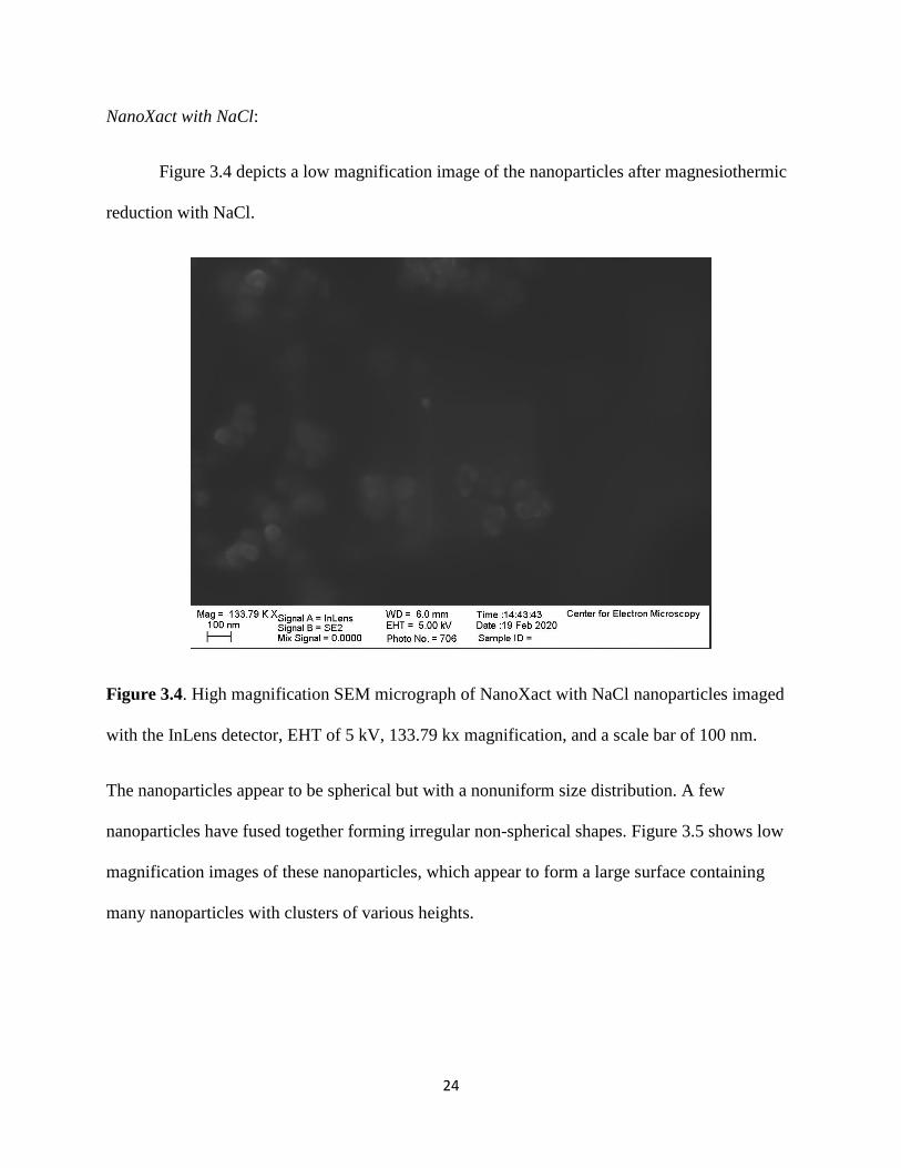
NanoXact with NaCl:
Figure 3.4 depicts a low magnification image of the nanoparticles after magnesiothermic
reduction with NaCl.
Figure 3.4. High magnification SEM micrograph of NanoXact with NaCl nanoparticles imaged
with the InLens detector, EHT of 5 kV, 133.79 kx magnification, and a scale bar of 100 nm.
The nanoparticles appear to be spherical but with a nonuniform size distribution. A few
nanoparticles have fused together forming irregular non-spherical shapes. Figure 3.5 shows low
magnification images of these nanoparticles, which appear to form a large surface containing
many nanoparticles with clusters of various heights.

25
Figure 3.5. Low magnification SEM micrographs of NanoXact with NaCl nanoparticles, EHT of
5 kV, and a 27.79 kx magnification. Left: InLens detector and a scale bar of 1 um. Right: SE2
detector and a scale bar of 1 um.
Increasing the magnification at this location results in the micrographs displayed in figure 3.6.
The image on the bottom has distortion, but both images display spherical particles. It is
challenging to determine if the nanospheres have fused or if the topological information is lost
from the InLens detector. The secondary detector was unable to image the sample at higher
magnification.

26
Figure 3.6. SEM micrographs of NanoXact with NaCl nanoparticles imaged at the same location
with EHT of 5 kV. Top: lower magnification micrograph, 73.09 kx; scale bar of 300 nm.
Bottom: higher magnification micrograph, 217.75 kx; scale bar of 100 nm.

27
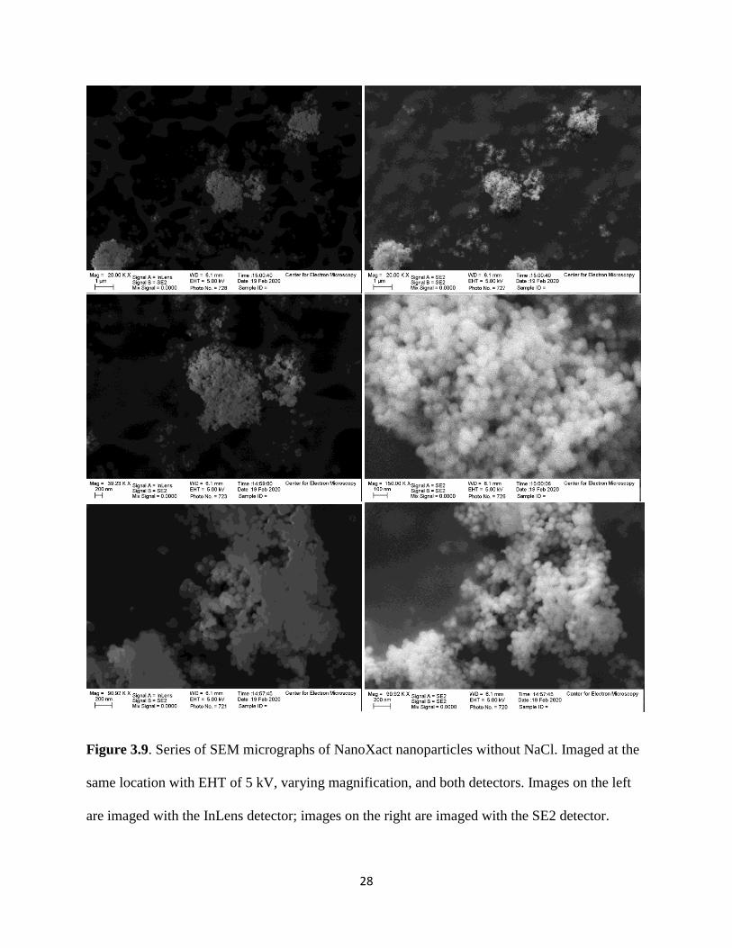
NanoXact without NaCl:
At low magnification, the NanoXact nanoparticles following magnesiothermic reduction without
NaCl as a heat sink look clustered together in clusters of varying sizes.
Figure 3.7. Low magnification SEM micrograph of NanoXact nanoparticles without NaCl, EHT
of 5 kV, InLens detector, a 20 kx magnification, and a 1 um scale bar.
At higher magnification, the NanoXact particles without NaCl as a heat sink appear to have
retained morphology as displayed in Figures 3.8 and 3.9.
Figure 3.8. SEM micrographs of NanoXact nanoparticles without NaCl, EHT of 5 kV, a scale
bar of 100 nm, and InLens detector. Left: 70 kx magnification. Right: 150 kx magnification.
28
Figure 3.9. Series of SEM micrographs of NanoXact nanoparticles without NaCl. Imaged at the
same location with EHT of 5 kV, varying magnification, and both detectors. Images on the left
are imaged with the InLens detector; images on the right are imaged with the SE2 detector.

29
NanoXact with NaCl after HF etch:
Figure 3.10. Series of SEM micrographs of NanoXact nanoparticles with NaCl after the HF
etching process imaged at EHT of 2.55 kV. Top micrographs were imaged at the same location
with 20 kx magnification and a scale bar of 1 um. The top left was imaged with the InLens
detector, and the right was imaged with the SE2 detector. The bottom micrograph was imaged at
70 kx and a scale bar of 100 nm with the InLens detector.
30
After magnesiothermic reduction with NaCl, the NanoXact particles were etched with HF
to eliminate any silica byproduct. The low magnification images in Figure 3.10 display varying
sizes of silicon clusters. We were unable to image higher magnifications of the NanoXact
nanoparticles with NaCl after the HF etch due to image distortion, but at 70 kx magnification, the
particles appear to be fused, forming amorphous shapes.
NanoXact without NaCl after HF etch:
Similarly to the NanoXact nanoparticles with NaCl after the HF wash, the NanoXact
nanoparticles without NaCl after the HF etch appear to be amorphous, as depicted in Figures
3.11 and 3.12.

31
Figure 3.11. Series of SEM micrographs of NanoXact nanoparticles without NaCl after the HF
etching process imaged at EHT of 2.55 kV with the InLens detector. The top left was imaged
with 20kx, and a scale bar of 1 um. The top right was imaged at 70 kx with a 100 nm scale bar.
The following images were imaged at 150 kx, 275 kx, and 300 kx with scale bars of 100 nm, 100
nm, and 30 nm respectively.

32
Figure 3.12. Series of SEM micrographs of NanoXact nanoparticles with NaCl after the HF
etching process imaged at EHT of 2.55 kV with the InLens detector. The top left micrograph was
imaged at 1.75 kx, and a scale bar of 10 um. The following images have a scale bar of 100nm.
The top right was imaged with 70 kx magnification. The bottom left micrograph was imaged at
150 kx, and the bottom right was imaged at 275 kx magnification.

33
Stöber:
The Stöber nanoparticles prior to magnesiothermic reduction are solid and spherical, as
depicted in Figures 3.13 and 3.14.
Figure 3.13. Series of SEM micrographs of Stöber nanoparticles imaged at EHT of 10 kV with
the InLens detector. The top micrograph was imaged at 2.81 kx and a scale bar of 3 um. The

34
bottom left micrograph was imaged at 20 kx and a scale bar of 1 um. The bottom right was
imaged at 75 kx magnification and a scale bar of 100 nm.
Figure 3.14. Series of SEM micrographs of Stöber nanoparticles imaged at EHT of 10 kV. The
top micrographs were imaged at the same location, 20 kx magnification, and a scale bar of 1 um.
The top left was imaged with the InLens detector, and the top right was imaged with the SE2
detector. The bottom micrograph was imaged at 151.57 kx and a scale bar of 100 nm with the
SE2 detector.

35
Stöber with NaCl:
Following magnesiothermic reduction with NaCl as a heat sink, the Stöber nanoparticles
retained morphology in comparison to the starting material. However, there are impurities or
fusion of particles, as seen in Figures 3.15 and 3.16.
Figure 3.15. SEM micrographs of Stöber nanoparticles with NaCl imaged at EHT of 5 kV with
the InLens detector. The top micrograph was imaged at 20 kx and has a scale bar of 1 um. The
bottom micrograph was imaged at 150 kx and has a scale bar of 100 nm.

36
Figure 3.16. SEM micrographs of Stöber nanoparticles with NaCl imaged at EHT of 5 kV. The
top micrographs were imaged at the same location, have a scale bar of 1 um, and 20 kx
magnification. The bottom micrographs were imaged at the same location, with 186.60 kx and a
scale bar of 100 nm. Images on the left: InLens, images on the right: SE2.

37
Stöber without NaCl:
Stöber nanoparticles that did not have NaCl as a heat sink fused together and became
amorphous as displayed in Figures 3.17, 3.18, and 3.19.
Figure 3.17. SEM micrographs of Stöber nanoparticles without NaCl imaged at EHT of 5 kV
and the InLens detector at the same location with varying magnification. The magnification is
8.75 kx, 20 kx, 70 kx, and 150 kx with a scale bar of 1 um, 1 um, 100nm, and 100nm,
respectively.

38
Figure 3.18. SEM micrographs of Stöber nanoparticles without NaCl imaged at EHT of 5 kV
and the InLens detector at the same location, scale bar of 100 nm, and 150 kx magnification.

39
Figure 3.19. SEM micrographs of Stöber nanoparticles without NaCl imaged at EHT of 5 kV at
the same location with 20 kx magnification and a scale bar of 1 um. Top: InLens detector.
Bottom: SE2 detector.
40
Stöber with NaCl after HF etch:
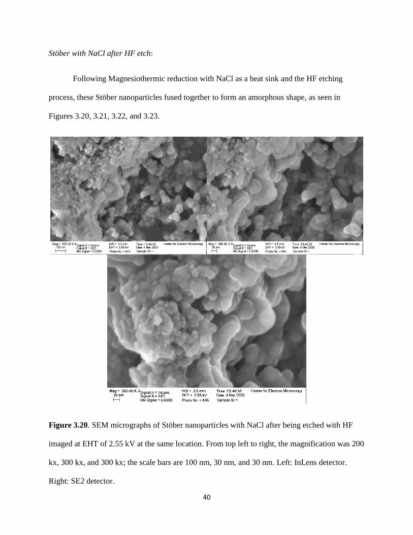
Following Magnesiothermic reduction with NaCl as a heat sink and the HF etching
process, these Stöber nanoparticles fused together to form an amorphous shape, as seen in
Figures 3.20, 3.21, 3.22, and 3.23.
Figure 3.20. SEM micrographs of Stöber nanoparticles with NaCl after being etched with HF
imaged at EHT of 2.55 kV at the same location. From top left to right, the magnification was 200
kx, 300 kx, and 300 kx; the scale bars are 100 nm, 30 nm, and 30 nm. Left: InLens detector.
Right: SE2 detector.

41
Figure 3.21. SEM micrographs of Stöber nanoparticles with NaCl after being etched with HF
imaged at EHT of 2.55 kV at the same location with the InLens detector. Top left: 20 kx with a
scale bar of 1 um. Top right: 70 kx, scale bar of 100 nm. Bottom: 150 kx, scale bar of 100 nm.

42
Figure 3.22. SEM micrograph of Stöber nanoparticles with NaCl after being etched with HF
imaged at EHT of 2.55 kV with the InLens detector, a magnification of 1.00 kx, and scale bar of
10 um.

43
Figure 3.23. SEM micrograph of Stöber nanoparticles with NaCl after being etched with HF
imaged at EHT of 2.55 kV with the InLens detector. Top left: 20 kx magnification and a scale
bar of 1 um. The following images have a scale bar of 100 nm. Top right: 70 kx magnification.
Bottom left: 150 kx magnification. Bottom right: 275 kx magnification.
Some nanoparticles isolated from the cluster appear to have retained spherical morphology, as
illustrated in Figure 3.24.

44
Figure 3.24. SEM micrograph of Stöber nanoparticles with NaCl after being etched with HF
imaged at EHT of 2.55 kV, with a scale bar of 100 nm, and imaged with the InLens detector.
Top: 178.44 kx magnification. Bottom: 275 kx magnification.

45
Stöber without NaCl after HF etch:
When NaCl was used as a heat sink during magnesiothermic reduction, then etched with
HF, the Stöber nanoparticles appear amorphous and fused together as depicted in Figures 3.35,
3.26, and 3.27.
Figure 3.25. SEM micrograph of Stöber nanoparticles without NaCl after being etched with HF
imaged at EHT of 2.55 kV with the InLens detector, a scale bar of 1 um, and 20 kx
magnification.

46
Figure 3.26. SEM micrograph of Stöber nanoparticles without NaCl after being etched with HF
imaged at EHT of 2.55 kV with the InLens detector at the same location. Top left: 20 kx
magnification and a scale bar of 1 um. Top right: 70 kx magnification and a scale bar of 100 nm.
Bottom left: 150 kx magnification and a scale bar of 100 nm. Bottom right: 275 kx magnification
and a scale bar of 30 nm.

47
Figure 3.27. SEM micrograph of Stöber nanoparticles without NaCl after being etched with HF
imaged at EHT of 2.55 kV with the InLens detector at the same location. Top left: 20 kx
magnification and a scale bar of 1 um. Top right: 70 kx magnification and a scale bar of 100 nm.
Bottom left: 150 kx magnification and a scale bar of 100 nm. Bottom right: 300 kx magnification
and a scale bar of 30 nm.
In a different region of the sample, a honeycomb-like structure is visible, as imaged in
Figures 3.28, 3.29, and 3.30.

48
Figure 3.28. SEM micrograph of Stöber nanoparticles without NaCl after being etched with HF
imaged at EHT of 2.55 kV at the same location, 20 kx, and 1 um scale bar. Top: InLens detector.
Bottom: SE2 detector.

49
Figure 3.29. SEM micrograph of Stöber nanoparticles without NaCl after being etched with HF
imaged at EHT of 2.55 kV at the same location. All of the images on the left: InLens. All images
on the right: SE2. Top images: 8 kx magnification, 1 um scale bar. The following images have a
100 nm scale bar. Middle images: 70 kx magnification. Bottom images: 150 kx magnification.

50
Figure 3.30. SEM micrograph of Stöber nanoparticles without NaCl after being etched with HF
imaged at EHT of 2.55 kV with the InLens detector, a 100 nm scale bar, and 275 kx
magnification.
Table 3.1 Summary of experimental results.
Spherical Fused Amorphous Honeycomb
Starting Materials
1 Stöber x
2 NanoXact x
Magnesiothermic Reduction with NaCl
3 Stöber x x
4 NanoXact x x
Magnesiothermic Reduction without NaCl
5 Stöber x x x
6 NanoXact x x
Etching with HF
7 Stöber (NaCl) x x x
8 Stöber x
9 NanoXact (NaCl) x x x
10 NanoXact x x
Table 3.1 displays the morphological differences of the nanoparticles throughout the experiment.

51
4. DISCUSSION
The starting materials commercially available NanoXact and lab synthesized Stöber
nanoparticles are both spherical. Significant observations include that there was retention of
morphology on a nanoscale similar to starting material without using the HF etching process,
regardless of the addition of NaCl. NaCl used as a heat sink does cause a few spherical objects to
appear. However, the magnesiothermic reduction does create many amorphous structures. The
nanoparticles after the HF etching process are believed to be pure elemental silicon. The holes
may be the location of silica that was etched away with HF, after HF etching morphology is
retained/ ragged. The Stöber particles without NaCl as a heat sink created honeycomb-like
structures with some impurities.
The InLens has a higher S:N ratio than the SE2 detector, and the SE2 detector portrays
enhanced topography in comparison to the InLens detector. There were difficulties in imaging
the NanoXact nanoparticles with NaCl.
5. CONCLUSION
For both the commercially available NanoXact and laboratory synthesized Stöber
nanoparticles prior to magnesiothermic reduction, the nanoparticles appear solid and spherical.
Following magnesiothermic reduction, morphology is preserved with or without NaCl as a heat
sink. However, Stöber nanoparticles without NaCl as a heat sink also appeared to fuse together
while retaining some morphology from the starting material. Following the HF etching process,
NanoXact and Stöber nanoparticles with NaCl were amorphous and fused together. The
NanoXact nanoparticles without NaCl that were etched with HF appear amorphous, but due to
the low magnification limitation, it is difficult to deduce if the nanoparticles are fused or partially

52
spherical. The Stöber nanoparticles without NaCl after the HF etch have a honeycomb-like
structure with some impurities. Both NanoXact and Stöber nanoparticles after magnesiothermic
reduction with and without NaCl as a heat sink retained a spherical morphology similar to the
starting material. Once the HF etching process is completed, it is challenging to retain
morphology. A majority of the experiment produced results we were not looking for. However,
if the honeycomb structure of the Stöber nanoparticles without NaCl after HF etch could be
replicated without impurities, they could be manufactured to increase surface area for silicon
anodes on batteries.
6. FUTURE WORK
Since the Stöber process should be size, shape, and morphology preserving, future
experiments could include varying reaction conditions that produce solid crystalline cores while
maintaining spherical shape. Altering SEM parameters may increase resolution, or higher
resolution can be achieved using a more powerful SEM. The goal would be to vary reaction
conditions that produce solid crystalline cores while maintaining spherical shape. It would be
interesting to determine similarities to the starting material, and whether the nanoparticles were
actually solid or porous. Since there was an XRD mismatch, SEM would be used to determine
the mismatch. Use of PELCO Tabs 12mm OD instead of carbon tape to image nanoparticles may
increase the quality of the images deterring image distortion. EDX could be used to determine if
SiO2 is a byproduct following magnesiothermic reduction with and without NaCl after
magnesiothermic reduction; additionally, it can be used for the same reason following the HF
etch. Silicon is more conductive than silica, so it may be easier to image Si due to a reduction in
charging effects. Another question to consider would be how and why does surface area increase
in silicon after magnesiothermic reduction?

53
7. ACKNOWLDGEMENTS
Dr. Goforth, James Barnes, The Goforth Lab, CEMN, Greg Baty, Dr. Chen, and The PSU
Physics Department.

54
8. REFERENCES
1 Entwistle, J., Rennie, A., & Patwardhan, S. (2018). A review of magnesiothermic
reduction of silica to porous silicon for lithium-ion battery applications and beyond.
Journal of Materials Chemistry A, 6(38), 18344–18356.
https://doi.org/10.1039/c8ta06370b
2 Plumeré, N., Ruff, A., Speiser, B., Feldmann, V., Mayer, H. A. (2012). Stöber silica particles as
basis for redox modifications: Particle shape, size, polydispersity, and porosity. Journal
of Colloid and Interface Science, 368(1), 208–
219.https://doi.org/10.1016/j.jcis.2011.10.070
3Lai, Y., Thompson, J. R., & Dasog, M. (2018). Metallothermic Reduction of Silica
Nanoparticles to Porous Silicon for Drug Delivery Using New and Existing Reductants.
Chemistry - A European Journal, 24(31), 7913-7920. doi:10.1002/chem.201705818
4Hadipour Moghaddam, S. P., Yazdimamaghani, M., & Ghandehari, H. (2018). Glutathione-
sensitive hollow mesoporous silica nanoparticles for controlled drug delivery. Journal of
controlled release : official journal of the Controlled Release Society, 282, 62–75.
https://doi.org/10.1016/j.jconrel.2018.04.032
5Julian, M. M. (2015). Foundations of crystallography with computer applications. Boca Raton:
Taylor & Francis.
6Goldstein, J. I., Newbury, D. E., Michael, J. R., Ritchie, N. W., Scott, J. H., & Joy, D. C.
(2018). Scanning Electron Microscopy and X-Ray Microanalysis. New York, NY: Springer
New York.
7nanoComposix. Silica Surface. nanoComposix. https://nanocomposix.com/pages/silica-surface.

55
8Dasog, M., Yang, Z., & Veinot, J. G. (2012). Size-controlled solid state synthesis of
luminescent silicon nanocrystals using Stöber silica particles. CrystEngComm, 14(22),
7576. doi:10.1039/c2ce25950h
9Rapp, R.A., Ezis, A. & Yurek, G.J. Displacement reactions in the solid state. MT 4, 1283–1292
(1973). https://doi.org/10.1007/BF02644523