sanyo ce26 32lc d8120tv20 training brochure 72
DESCRIPTION
proprietarul a gasit telecomanda plasmei si mi-a trimis-o. Rezultatul: am avut dreptate, cineva s-a jucat si a activat protectia pentru copii drept care tastatura a fost dezactivata. Puteam sa sap eu in ea mult si bine.OVERVIEW & FAULT DIAGNOSIS 17MB22 ChassisCE26LC81-B CE26LD81-BCE32LC81-B CE32LD81-BSANYO LCD TV 2007-8PCB Spares Listing For the 2007-8 SANYO TV, ordering of spare parts needs reference taken not only of the TV model number i.e. CE32LD81-B but also of the actual Product Code and Production Code (Batch Number) of that particular model. On occasions the same model number could have a different particular Pcb or a different manufacturer or revision of LCD panel fitted. The ProTRANSCRIPT

CE26LC81-B CE32LC81-B
CE26LD81-B CE32LD81-B
SANYO LCD TV
OVERVIEW &
FAULT DIAGNOSIS
17MB22 Chassis


SANYO LCD TV 2007-8
PCB Spares Listing
For the 2007-8 SANYO TV, ordering of spare parts needs reference taken not only of the TV model number i.e. CE32LD81-B but also of the actual Product Code and Production Code (Batch Number) of that particular model. On occasions the same model number could have a different particular Pcb or a different manufacturer or revision of LCD panel fitted. The Product code and Production Code could be viewed similarly to previous models whereby production changes were notified by use of a different service code i.e. CE32LD6-B-01. The required codes can be easily found on the rating plate on the TV back cabinet under the Model number and 2 bar codes as seen below.
Product Code
Identification of Production Code (26” Example)
During a production run with a particular Product Code, different LCD panels or Pcb’s may be fitted. Each of the changes will have a particular Production Code or Batch Number. (Shown above in blue). Therefore the correct ‘Product Code’ and ‘Production Code numbers’ must be used to locate the correct part numbers, otherwise incorrect parts may be supplied. Display Panel Inverter and Control Pcb’s will be supplied subject to availability. You must consult the appropriate parts list table for information before ordering any parts, otherwise incorrect parts may be supplied.
Production Code (Batch No.)
TV RATING PLATE

Signal Pcb (Chassis) Identification (42” Example)
Cabinet Back Rating Plate
Product Code Part Number
LCD Panel Size - 42”
Main (Chassis) Pcb
LCD Panel Manufacturer (LG in this example)
Production Code (Batch No.) 2 + 1st 7 digits of SN
This shows pcb correct for this model
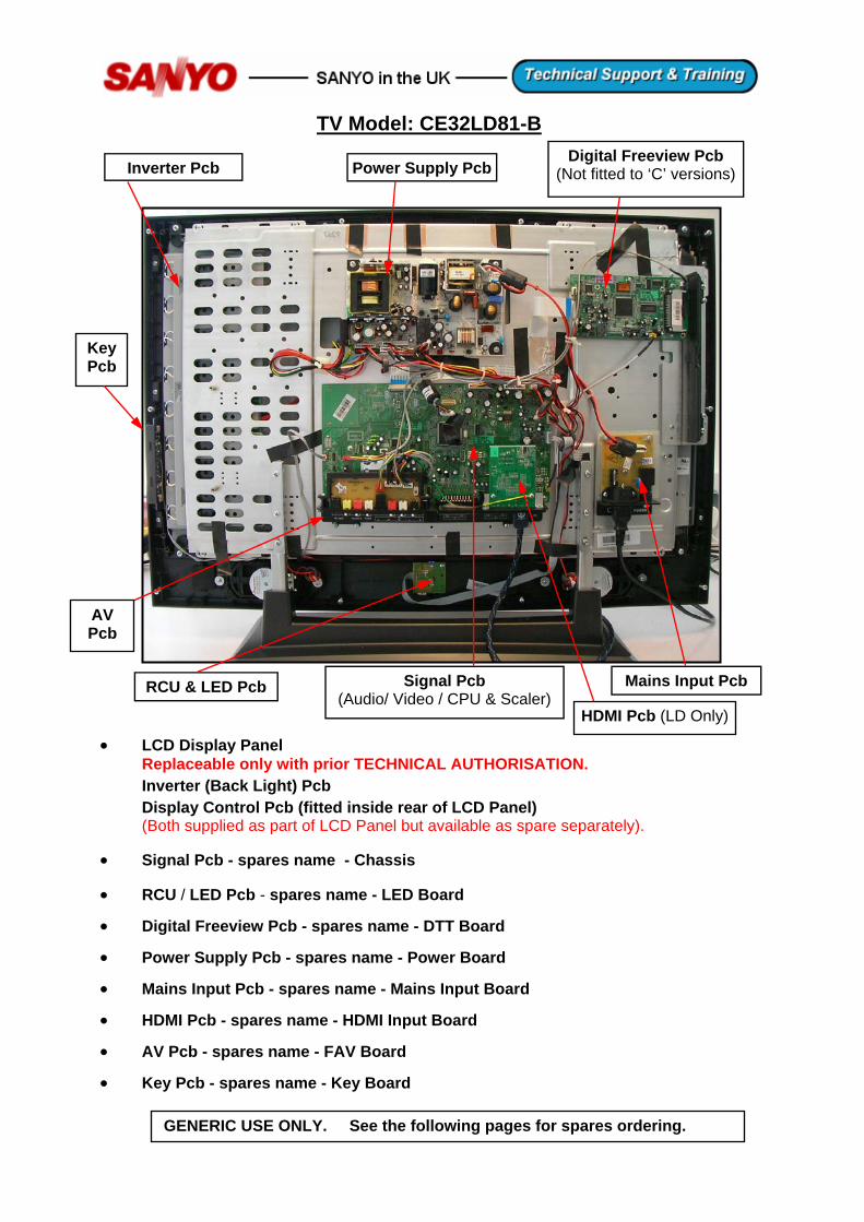
• LCD Display Panel Replaceable only with prior TECHNICAL AUTHORISATION.
Inverter (Back Light) Pcb
Display Control Pcb (fitted inside rear of LCD Panel) (Both supplied as part of LCD Panel but available as spare separately).
• Signal Pcb - spares name - Chassis
• RCU / LED Pcb - spares name - LED Board
• Digital Freeview Pcb - spares name - DTT Board
• Power Supply Pcb - spares name - Power Board
• Mains Input Pcb - spares name - Mains Input Board
• HDMI Pcb - spares name - HDMI Input Board
• AV Pcb - spares name - FAV Board
• Key Pcb - spares name - Key Board
TV Model: CE32LD81-B
GENERIC USE ONLY. See the following pages for spares ordering.
Inverter Pcb
Signal Pcb (Audio/ Video / CPU & Scaler)
Power Supply Pcb Digital Freeview Pcb
(Not fitted to ‘C’ versions)
Mains Input Pcb RCU & LED Pcb
HDMI Pcb (LD Only)
Key Pcb
AV Pcb

CE32LD81-B MAINS INPUT PCB
IMPORTANT
If this Pcb is fitted, this product must be earthed
Chassis mounting screws with star washers are used to secure the mains A/C board to the chassis, thereby developing the class one earth bond to the
metal chassis from the mains input earth pin.
The star washers must be fitted to the points shown when re-fitting the mains input board.
Always check the continuity between the earth pin of the mains plug and the metal chassis after servicing.
Mains input Pcb fuse is T3.15A
This Pcb may not be fitted to later models and the mains cable is directly wired to the PSU Pcb.A latching standby button will also be fitted, giving a power save mode and switching off the front LED.
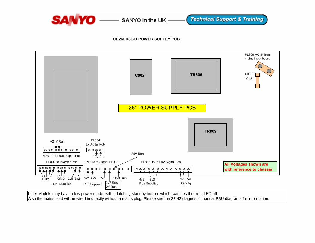
C902
PL809 AC IN frommains input board
F800T2.5A
PL803 to Signal PL003 PL805 to PL002 Signal Pcb
PL801 to PL001 Signal Pcb
PL804 to Digital Pcb
26" POWER SUPPLY PCB
12V Run
3v3 5V Standby
4v9 3v3Run Supplies
All Voltages shown are with reference to chassis
PL802 to Inverter Pcb
Run Supplies
34V Run
11v9 Run3v2 2v5 2v61v7 Stby0V Run
+24V 2v5 3v2Run Supplies
CE26LD81-B POWER SUPPLY PCB
Run Supplies
+24V Run
GND
TR803
TR806
Later Models may have a low power mode, with a latching standby button, which switches the front LED off.Also the mains lead will be wired in directly without a mains plug. Please see the 37-42 diagnostic manual PSU diagrams for information.

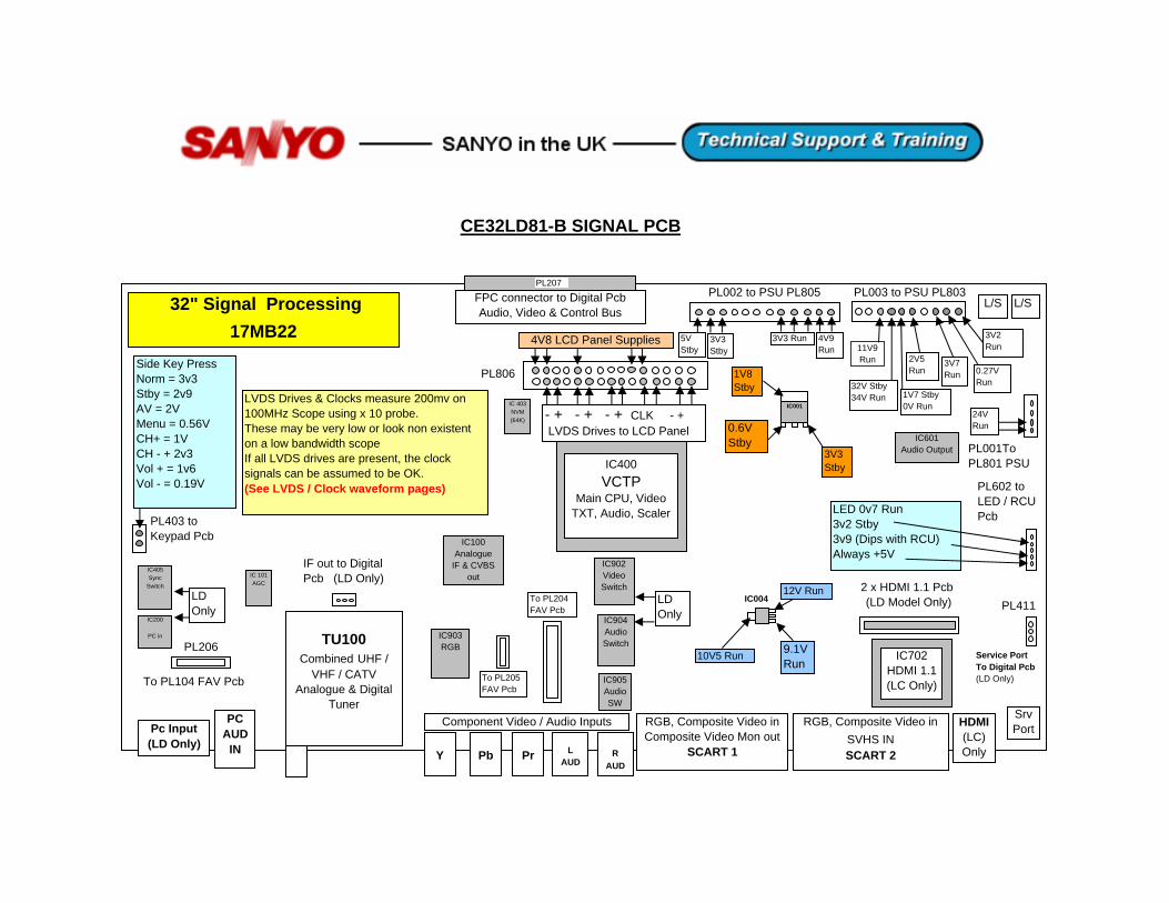
To PL302Digital Pcb
PL602 to LED / RCU Pcb
26" Signal Processing17MB22
TU100Combined UHF /
VHF / CATV Analogue & Digital
TunerPC
AUDIN Y Pb Pr L
AUDR
AUD
RGB, Composite Video inComposite Video Mon out
SCART 1
RGB, Composite Video inSVHS INSCART 2
L/SL/SFPC connector to Digital PcbAudio, Video & Control Bus
PL806
IF out to DigitalPcb (LD Only)
PL403 toKeypad Pcb
2 x HDMI 1.1 Pcb (LD Model Only)
Pc Input(LD Only)
To PL104 FAV Pcb
PL002 to PSU PL805 PL003 to PSU PL803
Component Video / Audio Inputs SrvPort
Service Port To Digital Pcb(LD Only)
IC400VCTP
Main CPU, VideoTXT, Audio, Scaler
IC702HDMI 1.1(LC Only)
HDMI(LC)Only
LVDS Drives & Clocks measure 200mv on 100MHz Scope using x 10 probe.These may be very low or look non existent on a low bandwidth scopeIf all LVDS drives are present, the clock signals can be assumed to be OK.(See LVDS / Clock waveform pages)
4V8 LCD Panel Supplies
- + - + - + CLK - + LVDS Drives to LCD Panel
PL206
IC 101AGC
IC100Analogue
IF & CVBS out
IC405Sync
Switch
IC200
PC in
LDOnly PL411
PL001To PL801 PSU
11V9Run
32V Stby34V Run 1V7 Stby
0V Run
3V2Run
2V5Run
2V5Run
5VStby
3V3Stby
4V9Run
3V3 Run
IC601Audio Output
IC903RGB
IC902VideoSwitch
IC904AudioSwitch
IC905AudioSW
LDOnly
To PL205FAV Pcb
To PL204FAV Pcb
24VRun
IC001
3V3Stby
1V8Stby
0.6V Stby
IC00412V Run
10V5 Run 9.1VRun
CE26LD81-B SIGNAL PCB
Side Key PressNorm = 3v3Stby = 2v9AV = 2VMenu = 0.56VCH+ = 1VCH - + 2v3Vol + = 1v6Vol - = 0.19V
IC 403NVM(64K)
2v9
LED 0v7 Run3v2 Stby3v9 (Dips with RCU)Always +5V
PL207
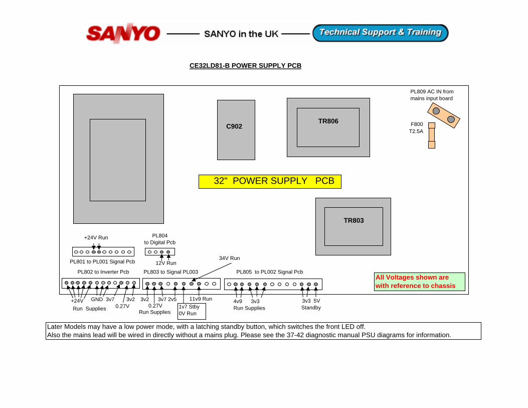
C902
PL809 AC IN frommains input board
F800T2.5A
PL803 to Signal PL003 PL805 to PL002 Signal Pcb
PL801 to PL001 Signal Pcb
PL804 to Digital Pcb
32" POWER SUPPLY PCB
12V Run
3v3 5V Standby
4v9 3v3Run Supplies
All Voltages shown are with reference to chassis
PL802 to Inverter Pcb
Run Supplies
34V Run
11v9 Run3v2 3v7 2v51v7 Stby0V Run
+24V
CE32LD81-B POWER SUPPLY PCB
Run Supplies
+24V Run
0.27VGND 3v7 3v2
TR803
TR806
0.27V
Later Models may have a low power mode, with a latching standby button, which switches the front LED off.Also the mains lead will be wired in directly without a mains plug. Please see the 37-42 diagnostic manual PSU diagrams for information.
To PL302Digital Pcb
PL602 to LED / RCU Pcb
32" Signal Processing17MB22
TU100Combined UHF /
VHF / CATV Analogue & Digital
TunerPC
AUDIN Y Pb Pr L
AUDR
AUD
RGB, Composite Video inComposite Video Mon out
SCART 1
RGB, Composite Video inSVHS INSCART 2
L/SL/SFPC connector to Digital PcbAudio, Video & Control Bus
PL806
IF out to DigitalPcb (LD Only)
PL403 toKeypad Pcb
2 x HDMI 1.1 Pcb (LD Model Only)
Pc Input(LD Only)
To PL104 FAV Pcb
PL002 to PSU PL805 PL003 to PSU PL803
Component Video / Audio Inputs SrvPort
Service Port To Digital Pcb(LD Only)
IC400VCTP
Main CPU, VideoTXT, Audio, Scaler
IC702HDMI 1.1(LC Only)
HDMI(LC)Only
LVDS Drives & Clocks measure 200mv on 100MHz Scope using x 10 probe.These may be very low or look non existent on a low bandwidth scopeIf all LVDS drives are present, the clock signals can be assumed to be OK.(See LVDS / Clock waveform pages)
4V8 LCD Panel Supplies
- + - + - + CLK - + LVDS Drives to LCD Panel
PL206
IC 101AGC
IC100Analogue
IF & CVBS out
IC405Sync
Switch
IC200
PC in
LDOnly PL411
PL001To PL801 PSU
11V9Run
32V Stby34V Run 1V7 Stby
0V Run
3V2Run
0.27VRun
3V7Run
2V5Run
5VStby
3V3Stby
4V9Run
3V3 Run
IC601Audio Output
IC903RGB
IC902VideoSwitch
IC904AudioSwitch
IC905AudioSW
LDOnly
To PL205FAV Pcb
To PL204FAV Pcb
24VRun
IC001
3V3Stby
1V8Stby
0.6V Stby
IC00412V Run
10V5 Run 9.1VRun
CE32LD81-B SIGNAL PCB
Side Key PressNorm = 3v3Stby = 2v9AV = 2VMenu = 0.56VCH+ = 1VCH - + 2v3Vol + = 1v6Vol - = 0.19V
IC 403NVM(64K)
LED 0v7 Run3v2 Stby3v9 (Dips with RCU)Always +5V
PL207
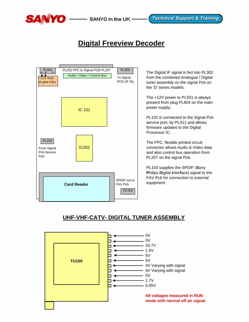
Digital Freeview Decoder
Card Reader
PL202 FPC to Signal PCB PL207
To Signal PCB (IF IN)
+12V from PL804 PSU
SPDIF out toFAV Pcb
From Signal Pcb Service Port
PL103
PL302PL501
PL102
IC 101
IC202
Audio / Video / Control Bus The Digital IF signal is fed into PL302 from the combined Analogue / Digital tuner assembly on the signal Pcb on the 'D' series models.
The +12V power to PL501 is always present from plug PL804 on the main power supply.
PL102 is connected to the Signal Pcb service port, by PL411 and allows firmware updates to the Digital Processor IC.
The FPC, flexible printed circuit connector allows Audio & Video data and also control bus operation from PL207 on the signal Pcb.
PL103 supplies the SPDIF (Sony Philips Digital Interface) signal to the FAV Pcb for connection to external equipment
UHF-VHF-CATV- DIGITAL TUNER ASSEMBLY
TU100
0V0V33.7V1.5V5V5V4V Varying with signal4V Varying with signal0V1.7V0.05V
All voltages measured in RUN mode with normal off air signal.
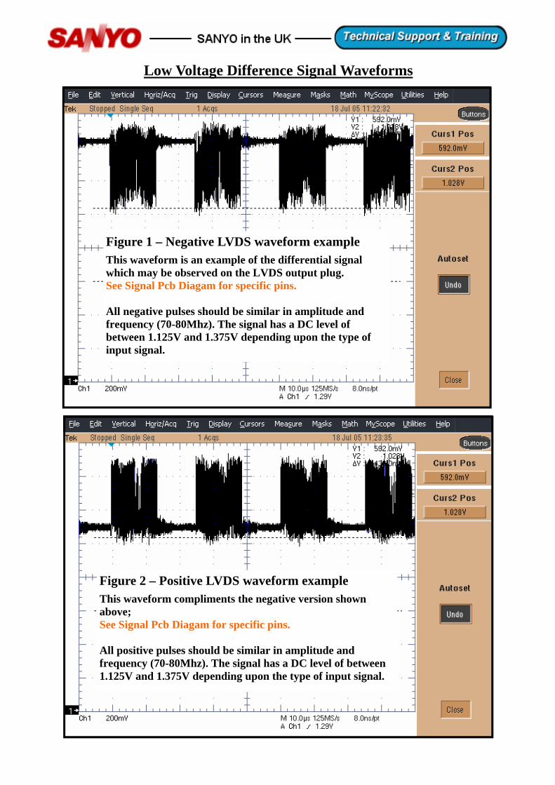
Low Voltage Difference Signal Waveforms
Figure 1 – Negative LVDS waveform example
This waveform is an example of the differential signal which may be observed on the LVDS output plug. See Signal Pcb Diagam for specific pins. All negative pulses should be similar in amplitude and frequency (70-80Mhz). The signal has a DC level of between 1.125V and 1.375V depending upon the type of input signal.
Figure 2 – Positive LVDS waveform example
This waveform compliments the negative version shown above; See Signal Pcb Diagam for specific pins. All positive pulses should be similar in amplitude and frequency (70-80Mhz). The signal has a DC level of between 1.125V and 1.375V depending upon the type of input signal.
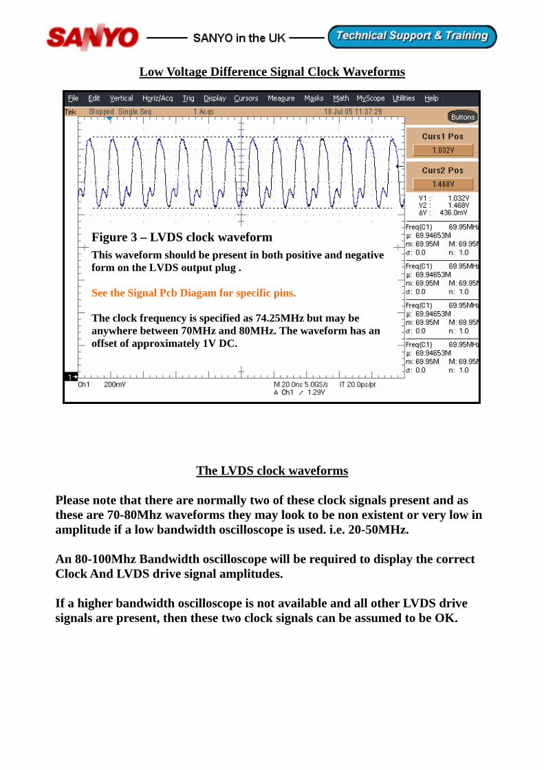
Low Voltage Difference Signal Clock Waveforms
Figure 3 – LVDS clock waveform
This waveform should be present in both positive and negative form on the LVDS output plug . See the Signal Pcb Diagam for specific pins. The clock frequency is specified as 74.25MHz but may be anywhere between 70MHz and 80MHz. The waveform has an offset of approximately 1V DC.
The LVDS clock waveforms Please note that there are normally two of these clock signals present and as these are 70-80Mhz waveforms they may look to be non existent or very low in amplitude if a low bandwidth oscilloscope is used. i.e. 20-50MHz. An 80-100Mhz Bandwidth oscilloscope will be required to display the correct Clock And LVDS drive signal amplitudes. If a higher bandwidth oscilloscope is not available and all other LVDS drive signals are present, then these two clock signals can be assumed to be OK.

NO SOUND OR PICTURE
Yes No
FAULTY SOUND - PICTURE OK
Dead Set or Stuck in Standby
Is front LED lit
check T3.15A fuse on mains input Pcb. If this is blown and blows again, replace mains input Pcb.If OK, check T2.5A fuse on PSU. If 2.5A fuse is blown and blows again, replace PSU.
If fuses OK, check for 240V AC at PL809 on PSU. If not present, check for O/C on/off switch etc.
If 240V AC Ok , check PSU Standby voltages at signal Pcb plugs PL002 and PL003.(See Signal Pcb diagram).
If voltages OK replace Signal Pcb. If incorrect then replace the PSU.
Check with RCU, if set comes on replace the TV Keypad Pcb.
If set comes on via the keypad, but not the RCU, then check the RCU and if OK, replace the LED / RCU Pcb.(see signal Pcb diagram PL602 for voltages)
Check Signal Pcb for all correct Standby voltages at PL002 and PL003. (See Signal PCB Diagram).
If incorrect check wiring to PSU, If OK, replace PSU PCB.
If OK replace the Signal Pcb.
No or Distorted Sound Output from all Sources
Check all Run voltage supplies from PSU at the Signal Pcb (See Signal Pcb Diagram)
If incorrect check PSU suppliesIf all OK. Replace faulty loudspeaker, or replace Signal Pcb.

Yes No
Yes No
NO PICTURE - NO OSD - SOUND OK
Are Backlights Lit ?
No Picture from TVor any AV inputs. No OSD. Sound OK
Check all voltages to the Inverter Pcb at PSU PL802 and Run voltages at PL803 & PL805. (See PSU diagram)
If all voltages from the PSU are OK, check the inverter Pcb for D/J or replace.
If after replacing the inverter Pcb, the backlights are still not lit, then one or more of the backlight lamps could be faulty.
If PSU voltages are incorrect, then replace PSU Pcb.
Check the five LCD panel +Ve supplies at Main Pcb LVDS LCD panel connector PL806.(See Signal Pcb diagram).
Also check all eight LVDS and two CLK waveforms with scope at LCD panel connector. (see Signal Pcb and LVDS diagrams)
If OK, do continuity check on LVDS cable.
If cable OK, try replacement display control pcb (top rear of LCD panel under metal cover). If still faulty then replace the LCD Panel assy.
If voltages / waveforms not OK then check all supplies on the Signal Pcb at PL002 and PL003. (see Signal Pcb diagram). If voltages OK, replace the Signal Pcb.
If voltages incorrect replace the PSU
If one channel of the inverters is not functioning due to a faulty inverter Pcb or a faulty lamp, then the backlights will light initially and then the inverter board will shut down with no picture, but the sound will still be present if previously tuned in.

Produced in the UK by
Mike Burnett Senior Technical Liaison & Training Engineer
SANYO Europe Ltd