run-time self-reconfigurable 2d convolver for adaptive image processing
TRANSCRIPT

Microelectronics Journal 42 (2011) 204–217
Contents lists available at ScienceDirect
Microelectronics Journal
0026-26
doi:10.1
n Corr
E-m
journal homepage: www.elsevier.com/locate/mejo
Run-time self-reconfigurable 2D convolver for adaptive image processing
Francisco Fons n, Mariano Fons, Enrique Canto
Department of Electronic, Electrical and Automatic Control Engineering, University Rovira i Virgili, Av. Paısos Catalans, 26, 43007 Tarragona, Spain
a r t i c l e i n f o
Article history:
Received 5 April 2010
Received in revised form
30 July 2010
Accepted 9 August 2010Available online 17 September 2010
Keywords:
FPGA
2D convolver
Embedded system
Run-time self-reconfiguration
Real-time image processing
Parallel processing
92/$ - see front matter & 2010 Elsevier Ltd. A
016/j.mejo.2010.08.008
esponding author.
ail address: [email protected]
a b s t r a c t
Two-dimensional (2D) convolution is a basic operation in digital signal processing, especially in image
and video applications. Although its computation is conceptually simple, a sum of products of constants
by variables, its implementation is highly demanding in terms of computational power, especially when
addressed to real-time embedded systems. This work brings an innovative approach oriented to
dynamically reconfigurable hardware. A flexible 2D convolver is deployed on a SRAM-based FPGA split
in two parts: a static region and a partially reconfigurable region (PRR). Just to provide a universal
solution, all the configurable aspects of the convolver (kernel dimensions, operands resolution, constant
coefficients, pipeline stages, etc.) fit allocated in the PRR. In this way, the computer can self-adapt its
structure on the fly, according to the characteristics of the image to be processed each time. Although
there are many research articles in the literature encompassing the design of 2D convolution
computers, to the best of the authors’ knowledge, this is the first work that implements a 2D convolver
based on run-time reconfigurable hardware, while other approaches synthesize it either directly in
software or in hardware as fully static designs. This pioneer alternative – exploiting key
implementation aspects like parallelism, pipeline, flexibility and functional density – overcomes both
computational performance of software solutions and cost-effectiveness of static hardware designs,
while delivering an outstanding level of adaptability. The balanced time-area trade-off achieved with
this technology makes it appropriate for high-performance low-cost embedded systems.
& 2010 Elsevier Ltd. All rights reserved.
1. Introduction
General-purpose microprocessors founded on Von Neumannarchitectures are often addressed to compute 2D convolutions insoftware. Although it is a flexible solution, the transformation ofthe 2D convolution algorithm from its innate parallel computa-tional conception to a sequential software flow significantlydegrades its efficiency. This architectural mismatch is hidden inhigh-performance computing (HPC) platforms like PCs operatingat frequencies in the range of GHz. However, when porting suchan algorithm to microcontrollers running at tens of MHz, itsinappropriate architecture is made visible now in the way of poorperformance. This fact advises the designer to reject a puresoftware approach in favor of hardware/software co-design inapplication scenarios oriented to embedded systems with real-time constraints. On the other hand, an extremely rigid approachfocused on a hardware 2D convolver (2DC) with hard-codeddesign parameters like kernel dimensions (J,I), constants of thefilter (Kj,i) or signal bit-depth means to give a particular solutiononly, far from being adaptable to different convolution require-
ll rights reserved.
(F. Fons).
ments claimed at the same time in an image processingapplication.
By nature, a 2D image convolution delimited by a spatialJ� I kernel (J¼2n+1, I¼2m+1, n40, m40) demands a high levelof parallelism of both product and addition operations, just as itsmathematical expression denotes:
puðy,xÞ ¼Xn
j ¼ �n
Xm
i ¼ �m
Kðj,iÞ � pðyþ j,xþ iÞ
where p is a generic pixel of the input Y�X image, Kj,i are thekernel weights applied to the J� I neighborhood of pixels centredat p, and p0 is the resultant convolved pixel of the output image.Moreover, a high bandwidth is needed for transferring data aslong as they are processed by the convolver, fact that points outtowards a pipeline implementation. Nevertheless, parallelism andpipelining are not the only design concerns; a further character-istic, flexibility, is demanded to the 2D convolution computer.Flexibility plays a fundamental role to empower the 2DC tosupport a large range of signal processing applications. Althoughfrom a structural point of view it holds its computational skeletoninvariant, depending on the processing stage, certain aspectslike constant coefficients (convolution function), type of filter (e.g.isotropic, quadrant symmetric, etc.), or kernel size (neighborhood)originate functional changes in the convolver which shall be
F. Fons et al. / Microelectronics Journal 42 (2011) 204–217 205
tailored to each particular case. All these requirements fit verywell with run-time reconfigurable computing technology, avail-able today in the market through self-reconfigurable fieldprogrammable gate arrays (FPGAs). Run-time partially reconfi-gurable FPGAs let balance all these design parameters in anoptimal way, exploiting hardware advantages such as parallelismand pipelining but without neglecting, in its turn, the flexibilitydelivered by software. Furthermore, along with the flexibilityaspect of the reconfigurable hardware, another important char-acteristic of partial reconfiguration (PR) is its cost-effectiveness,derived from the increased functional density of the hardwareresources. PR allows reconfiguring a portion of the FPGA on thefly, without disrupting the rest of FPGA resources that continue inoperation, which improves its effective logic density by removingthe need to place in the FPGA functions that are not operative atthat moment. Instead, these functions can be stored in externalmemory and loaded as needed, on demand, to process differentcomputations each time. This reduces the required size of theFPGA by allowing more processing on a smaller FPGA, bymultiplexing in time the resources to increase its use, as well asreducing power consumption in contrast to the classical approachbased on a static design where all the coprocessors required bythe application are placed in space for all the application life cycle,even for instants that are not being used. With these criteria inmind, this work explores the performance and architecturaltrade-off involved in the design of a run-time reconfigurableFPGA-based 2D convolution processor.
2. Related work
Software architectures oriented to 2D convolutions are usuallydiscarded in time-critical scenarios such as real-time imageprocessing applications. The reason is, basically, the high penaltyin time caused by the sequential execution of code to perform anarithmetic sum of products on a Von Neumann platform. Anotheroption in the market is the use of DSP processors. Even with theirmultiple single-cycle multiply-and-accumulate capability at GHzclock rates, e.g. TMS320C6457, the fact of completing the full2D-convolution in several instruction cycles results also in aninadmissible system overhead in certain applications. Oncediscarded sequential alternatives, the design of efficient architec-tures oriented to parallel 2D convolution processors has receiveda great deal of interest in the last years, and a lot of approacheshave been proposed for optimizing performance. Although thereare many examples of parallel 2DCs in the literature, only areduced number of them pay special attention to flexibilityaspects for targeting adaptive computers. In [1], for example, a2DC is proposed where the configurable kernel constants arestored in RAM. In other hardware approaches, flexibility isreached at expenses of more static hardware resources to letchoose among several alternatives at the same time [2]. The3�3 2DC presented in [3] is restricted to kernels with constantweights to be chosen among only 7 fixed values. This approachdoes not permit one to modify either those constant coefficientsor the data bit resolution, although it obtains different scalablekernel sizes by concatenating 3�3 convolvers. However, the easeof design offered by the dissection of a large convolution kernelinto smaller size kernels is obtained at the price of a larger overallcomplexity. The work presented in [4] deals with the implemen-tation of a 2DC oriented to isotropic kernels. As noted there, ifseveral adjacent convolutions are processed in parallel, then somepartial additions are repeated in the computing of those adjacentpixels in the image, which permits it to perform this addition onlyonce and reuse its result many times. However, the solutionpresented in that work is limited to 3�3 isotropic kernels, with
no chance of modifying the kernel size. A different approach of a3�3 2DC is developed in [5]. In that case, the convolver ischaracterized by the use of single instruction multiple data(SIMD) arithmetic circuits on an FPGA. It configures the bitresolution of pixels and kernel constants, selecting either theconvolution of one 3�3 kernel of 16-bit weights with 16-bitpixels or the processing in parallel of two adjacent 3�3convolutions on 8-bit pixels and 8-bit kernel weights. Thisselection is made by means of a control line connected to theconvolver. Later on, this work is extended in [6] by adding a newcontrol line that lets select the size of the kernel. This newflexibility is reached by interconnecting several copies of the basic3�3 convolver in a 2D grid. Thus, the new 2DC supports both3�3 and 5�5 convolutions for both 16- and 8-bit data. However,in these modular designs [3,6], the connection of functional blocksis not transparent and some additional shift registers – used asdelay lines to temporarily hold data – or multiplexers are neededto interconnect them. The main drawback of these architectures isprobably the high dependency of the convolver design with theown width of the image kernel to be processed. In other direction,in [7] it is proposed a 2DC that changes the constants of the kernelat real-time through a convolver implementation consisting oftwo components, namely a kernel generator that produces newkernel coefficients every clock cycle and a convolver thatperforms the computation. However, the transfer of the newkernels constants from the generator to the convolver itselfpenalizes in a high latency before the first convolution can beperformed.
Despite their titles, all the works overviewed until now are farfrom delivering a good level of adaptability; that is, they offer only avery limited flexibility and just for this reason they cannot beconsidered as general-purpose 2D convolution solutions. Our workpays special attention to this issue aimed at implementing a totallyflexible approach based on a SRAM-based FPGA powered by run-time partial reconfiguration technology. This work encompasses thedesign of a universal 2DC by building a library of hardware modules,described in VHDL hardware description language, to be processedin a run-time PR-FPGA. The convolver placed and routed in the FPGAcan be reconfigured at run-time – while the rest of the systemcontinues operating unaffected – in order to reach a fine tuning ofthe spatial filter applied, and using for this the same hardwareresources but adapted to the new circuitry required each time.Therefore, the 2DC design space exploration carried out in this workprovides a series of generic IP blocks that lets compose any 2Dconvolution of any kernel size and data resolution, only limited bythe own number of resources available in the defined FPGA partiallyreconfigurable region (PRR) where it keeps located. Each of these IPblocks is organized as a pipelined stage of the convolver architecturepresented in this work.
3. Run-time reconfigurable computing technology
SRAM-based FPGAs are volatile devices, i.e. they need to beconfigured each time they are powered up since they do notretain their configuration when power is removed. Dynamicallyreconfigurable SRAM-based FPGAs, furthermore, can conduct thisconfiguration not only at power up but also at any moment inexecution time.
Dynamic partial self-reconfiguration can be defined as theability granted to a programmable logic device to reconfiguresome portion of its resources at run-time, in background, whilethe rest of resources – not influenced by the reconfigurationprocess – continue their operation in foreground and keepexternal links alive, without the need to shut down the wholedevice during this update and restart afterwards the full system.

F. Fons et al. / Microelectronics Journal 42 (2011) 204–217206
Moreover, this reconfiguration is conducted by the device itself,i.e., autonomously, through specific modules placed inside theFPGA and, therefore, without requiring any support from externalprocessors. This technology allows exploiting all the potentialconceded to a SRAM-based FPGA given that the same piece ofsilicon can time-share a region of the device by swapping theredifferent functional tasks synthesized in hardware, to thus reusesuch resources. Behind this time-multiplexing of silicon areathere is a clear goal oriented to optimizing the resourcesbandwidth, where unused coprocessors are unloaded from theFPGA when they are not used to leave room for new ones,replacing idle or inactive hardware with other more usablecircuitry at that moment. This run-time optimization of thecircuitry allows a computation to fit into fewer hardwareresources. In the same direction, run-time reconfiguration is alsoused to partition a large special-purpose computing applicationonto limited FPGA resources; instead of using a static architecturethat maps on hardware, simultaneously, all the computationaltasks which that application gets decomposed in, several hard-ware partitions can be scheduled to sequentially load them – ondemand, as mutually exclusive processing tasks – in a smaller andless expensive FPGA. This run-time versatility, however, requiresplanning the synthesis of the whole application not only in space(hardware/software resources) but also in time (continuous usageof those resources). Thus, two design parameters must becarefully evaluated when deploying run-time reconfigurablecomputing technology:
�
The functional density of the programmable logic. It shall beconsidered in the phase of design conception and involves aspatial and temporal partitioning of the application in bothparallel and sequential tasks. � The reconfiguration latency of such time-multiplexedresources. The additional time for circuit reconfigurationinvolves designing a reconfiguration mechanism seamlesslymerged to the logic device to permit a fast access to its internalconfiguration memory. The efficient implementation of areconfiguration controller is a key point in the architecture ofrun-time reconfigurable systems, aimed at running thereconfiguration hidden to the application itself, withoutinvolving any overhead. There are many factors that influencethe reconfiguration throughput of an FPGA: (i) device techno-logical aspects like its internal structure (single- ormulti-context) or granularity (from full-reconfiguration topartial-reconfiguration with coarse- or fine-grain), (ii) techni-cal characteristics of the configuration interface that delimitthe reconfiguration bandwidth, such as data bus width (1-bit,8-bit, 32-bit, etc.), reconfiguration frequency (50, 100 MHz,etc.), or its accessibility (reconfiguration handled either by anexternal processor or by means of an internal processorsynthesized within the FPGA), and even (iii) size of the partialbitstream, which basically depends on the size of thereconfigurable region and the design complexity of thepartially reconfigurable module (PRM) to be downloadedthere.
3.1. Functional density
FPGA capacity is conventionally measured in terms of logiccells, i.e., LUTs and flip-flops, since this measure has a directextrapolation into combinational and sequential elements tosynthesize a specific functional algorithm or application. Thisnotion of logic cell utilization is, however, a purely spatial metric,which ignores the temporal aspect of logic cell usage. That is, itsays nothing about how often each logic cell is actually used.
Taking the temporal usage of a logic cell into account, it isadmitted that each gate has a capacity defined by its bandwidth.Exploiting this temporal aspect of capacity is necessary to extractthe most performance out of reconfigurable devices. In its turn,this temporal view lets estimate the effective cost of a resource.The functional density metric was introduced to balance theadvantages of dynamic reconfiguration against its associatedreconfiguration costs [8]. This metric helps to evaluate run-timereconfiguration against other more conventional approaches andlets establish well-founded conclusions about which is the bestalternative to implement a specific application in accordance withits own functional requirements.
3.2. Reconfiguration latency
Another motivation for using dynamically reconfigurablehardware is to reduce the execution time of algorithms thatwould otherwise be executed on software, involving for this asfew additional hardware resources as possible. But the improve-ments in efficiency provided by run-time reconfiguration are notavailable without cost and reconfiguration latency emerges as acritical parameter in the design of dynamically reconfigurablesystems used for algorithm acceleration. The reconfigurationlatency of dynamically reconfigurable hardware is defined as thetime that elapses between a request for a new circuitry to beloaded onto an already active FPGA and the point at which thenew circuitry is ready for use. This reconfiguration time overheadneeds to be evaluated early in the design cycle of dynamicallyreconfigurable applications. Consider the type of applications inwhich FPGAs are used to accelerate algorithms previouslyimplemented in software. It is possible that the dynamicswapping of circuits on and off in an FPGA will consumesignificant time relative to the processing time of the algorithmthat is being accelerated. This reconfiguration technique, if usedinappropriately, could potentially offset any speed-up gained inusing dedicated hardware in the first place. In this direction, thereexist several alternatives to deploy PR systems in function of thetime-area trade-off, depending on whether the efforts areaddressed to reduce the reconfiguration time to a minimum atexpenses of area (multi-context) or otherwise to minimize thearea and cost with an acceptable penalty in time (single-context):
�
In multi-context devices, the reconfiguration time overhead isbasically null, one clock cycle is usually enough to switch fromone hardware context to the next one. In these devices,however, the cost becomes apparent in area since, in order tominimize time, the device is architected with two or moreidentical hardware contexts, so this means that each config-urable bit is replicated as many times as hardware contexts thedevice has. In the market of the multi-context FPGAs, recently,a new startup, Tabula, announced its new family of devicesABAX provided with up to 8 different hardware contexts orstacked layers that can be swapped on the fly in some fewpicoseconds. � In single-context devices, additional time and memorybandwidths are required to transfer circuit configuration bitsfrom off-chip storage into the device configuration memory.In some cases, this extra time added to the processing timeof the application obviously mitigates the advantages of run-time specialization. Xilinx Virtex-4 devices, together withtheir successors Virtex-5 and Virtex-6, are at present the state-of-the-art concerning high-performance dynamic partialself-reconfiguration technology of commercial single-contextFPGA devices. Virtex-4 signified a serious advance regardingreconfiguration bandwidth in contrast to other previous FPGA

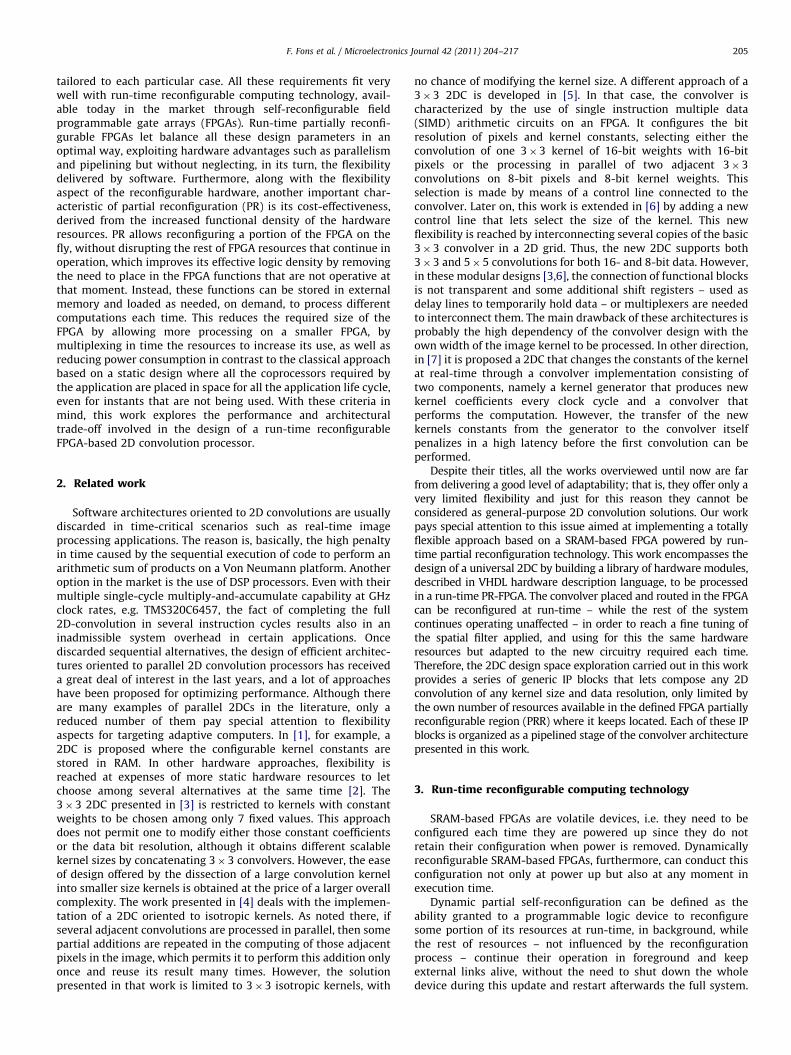
I/O BLOCK
LOGIC CELL
ROUTING RESOURCES
CONFIGURATION MEMORY CELLS
CLK BLOCK
Fig. 1. FPGA dual view: physical and application abstraction layers.
F. Fons et al. / Microelectronics Journal 42 (2011) 204–217 207
alternatives exploited in the past: it comes with a 32-bit databus interface qualified to self-reconfigure at run-time anyportion of the device at a maximum frequency of 100 MHz,which means a reconfiguration rate of 3.2 Gbps. Under thiscontext, this work presents the implementation of a reconfi-guration controller integrated into the FPGA system that isable to reach the maximum reconfiguration bandwidth ofVirtex-4 technology (32-bit @ 100 MHz), minimizing thus tothe utmost the impact of the reconfiguration process over theoverall execution time of the application.
Independent of the kind of run-time reconfigurable deviceused in the implementation of a specific high-performancecomputing system, in terms of time, the important point hereis to reach a total execution time (i.e. reconfigurationtime+processing time) that matches the requirements demandedby the end application. Besides, especially in embedded systems,this target shall be reached at the lowest possible cost. Both keyaspects – time and cost – have been taken into account in thiswork oriented to the implementation of an efficient and flexible2D convolution processor based on run-time reconfigurablehardware.
4. System architecture
Since their introduction, SRAM-based FPGAs have attractedspecial interest due to their potential as reconfigurable logic. Sucha device is equipped with a set of configurable hardwareresources distributed along its silicon area and connected to aSRAM configuration memory. Thus, all these resources areconfigured by downloading a sequence of bits (bitstream) intothe SRAM memory cells (internal registers). In this way, thebitstream defines the functionality granted to the FPGA resources
each time it is configured, and the reconfiguration simply consistsin reprogramming the configuration memory. In run-time PR-FPGAs, this reconfiguration can be performed affecting only aportion of the device (partial reconfiguration) and on the fly (run-time), while the rest of resources continue in operation.Furthermore, this reconfiguration can be handled by the FPGAitself (self-reconfiguration), i.e., without requiring the help of anyexternal processor. Taking into account these features, the FPGA ismodeled by two abstraction layers, as shown in Fig. 1:
�
Physical layer, constituted by the set of hardware resources(LUTs, interconnects, flip-flops, clock management blocks, I/Oblocks, RAM blocks, DSP blocks, etc.) present in the chip. � Application layer, related to the functionality, i.e., the ownbehavioral description of the application synthesized as abitstream and stored in the SRAM configuration memory.
The potential flexibility noticed in FPGAs, in contrast withASICs which are limited to one single static design or mask,incited the invention of this flexible hardware conception wheremany different algorithms can execute in turn on a single device,just as many different software algorithms can run on aconventional microprocessor. Like this, while an ASIC mustallocate area to implement every digital circuit the applicationrequires, regardless of how infrequently it is actually exercised, aPR-FPGA only needs be sized large enough to support the circuitsbeing active at any one time.
Although there exist several programmable logic devices fromdifferent suppliers in the market that support run-time partialreconfiguration today, e.g. Xilinx and Atmel vendors, the latestXilinx Virtex FPGA families, especially Virtex-4, -5 and -6,symbolize the state-of-the-art concerning available commercialPR-FPGA devices, basically due to their high-performance and

F. Fons et al. / Microelectronics Journal 42 (2011) 204–217208
large sizes able to allocate a full embedded system inside. Thesecharacteristics have led the research community to bet on the useof run-time partially reconfigurable FPGAs in many flexiblecomputing applications. In the meantime, another FPGA vendor,Altera, has recently announced the introduction, for the first timein its devices, of dynamic partial reconfiguration technology, justin the next-generation 28-nm Stratix-V family; at the same time,Xilinx also confirmed the fact that its next-generation 28-nm7-series FPGAs (Virtex-7, Kintex-7 and Artix-7 families) willsupport PR, thus becoming the fifth generation of Xilinx PRdevices in the market.
Being the fastest growing segment of the microelectronicssector, FPGA devices are rapidly moving into practically everyapplication field, such as automotive, telecommunications,defence, medical, chemistry, molecular biology, astrophysics,etc. Among them, specific niches like software-defined radio,cryptography, aerospace missions or optical transport networksolutions have showed their firm interest in exploiting PR. In thiswork, authors describe how a new application, a 2D convolutioncomputer, can be designed making use of PR technology tointegrate some flexible features of the processor into a reconfi-gurable region of a Xilinx Virtex-4 FPGA. The architecture of thissystem, although oriented to the 2D convolution application, isstandard and portable to many other high-performance low-costembedded applications, as presented next.
4.1. Functional components’ breakdown
Conceptually, our adaptive 2D convolver can be seen as aspecific coprocessor linked to a system CPU or host processor(typically a general-purpose microprocessor) with a specialcharacteristic: it can be reconfigured on the fly, thanks to thefact that it is instantiated in a reconfigurable region of a SRAM-based programmable logic device. However, the FPGA-based self-reconfigurable platform where the flexible 2D convolver issynthesized needs to fulfill certain requirements related to system
MPMC
MICROBLACPU
MMU MST
MMU SLV
NPI PLBV46
RECONF
DXCL
IXCL
XPS MCH EMC
TIMER
REG
FIFO
FIFO
FIFO
BM
BM
REG
REG
REG
BM
BM
PARTIA
MPMC
DDR-SDRAM
MICROBLACPU
MMU MST
MMU SLV
NPI PLBV46
REC
DXCL
IXCL
XPS MCH EMC
TIMER
REG
FIFO
LINEAR FLASH
FIFO
FIFO
BM
BM
REG
REG
REG
BM
BM
Fig. 2. System architecture and func
architecture and components’ breakdown. These characteristicsare generic for any embedded system based on run-timereconfigurable hardware technology. Thus, the flexible system iscomposed of a reduced amount of functional components, eachone with a specific role:
�
ZE
IGUR
INT
LLY R
ZE
ONFIG
IN
tion
A run-time reconfigurable FPGA synthesizes all the processingunits of the system, including the flexible 2D convolutioncoprocessor.
� External memories, both volatile and non-volatile, are requiredto store application data (processing images) and configurationdata (application settings and FPGA bitstreams), respectively.
� Also, a communication transceiver can be optionally used toestablish a permanent link between the system and theexterior world; for instance, in our case, a serial RS232interface lets transfer the resultant convolved images in BMPor TIF format to a personal computer.
The computational units of the system are embedded in aXilinx Virtex-4 XC4VLX25 device, a SRAM-based FPGA withdynamic partial reconfiguration capability. This device obeys, inour particular system, to a spatial partitioning of hardwareresources organized in two regions: (i) a partially reconfigurableregion (PRR), where the 2D convolver gets placed and can bereconfigured on the fly – as long as the application advances – bysimply changing the specific modules instantiated on theseresources to process different convolution computations in eachmoment and (ii) a static region, which keeps invariant for all thelife cycle of the application, basically composed of a soft-core32-bit MicroBlaze processor that plays the role of system CPU, anda reconfiguration controller responsible for reconfiguring the PRRon demand, while the rest of the system located in the staticregion keeps operating undisturbed.
The system components’ breakdown and their interconnec-tions are depicted in Fig. 2. In gray it is shown the differentchips out of the FPGA, i.e. the external memories and the
CONFIGURATION MEMORY
ATION CONTROLLER
DLMB
ILMB
XPS UARTLITE
CONTROLLER BRAM
SelectMAP
ICAP
ECONFIGURABLE REGION(PRR)
CONFIGURATION MEMORY
URATION CONTROLLER
DLMB
ILMB
XPS UARTLITE
PLATFORM FLASH
T CONTROLLER BRAM
SelectMAP
ICAP
RS232
al components breakdown.

F. Fons et al. / Microelectronics Journal 42 (2011) 204–217 209
communications transceiver in use. The rest of functional blocksin white correspond to different modules synthesized andmapped on resources of the FPGA. The MicroBlaze processor isequipped with standard peripherals like an interrupt controller, atimer, or a UART, all of them instantiated in the FPGA. Thememory controllers, required to access to the external non-volatile (flash) and DDR-SDRAM memories, are also implementedin the FPGA. All these components are interconnected through aCoreConnect PLBv46 multi-processor bus. Furthermore, theMicroBlaze processor is provided with instruction and datamemory caches in order to speed up there the processing of theprogram flow. Thus, both code and data are transferred fromexternal memory to the internal memory designated as cache andbuilt with internal RAM blocks of the FPGA. Apart from thesegeneric controllers and standard peripherals, the system iscomposed of two custom memory management units (MMU),one master and another slave, both implemented in VHDL. Themaster MMU is used to allow a direct memory access (DMA)transfer of data from the DDR-SRAM where the image is stored tothe PRR where the 2D convolution is processed. In this way, it ispossible to move the image data to the coprocessor placed in thePRR without involving the CPU, freeing it of this time-consumingtask. In fact, the MicroBlaze processor only takes part in accessingto the slave MMU to configure some registers used as configura-tion parameters of the 2D convolver, for instance the initialmemory address of the input image to be processed, or the sizeY �X of that image. Once the configuration of the 2D convolver isdone, the CPU only needs to give the go-ahead command to themaster MMU. From that moment on, the MMU starts the transferof the input image to the 2D convolver and this one carries out theimage convolution. Finally, when the computation is over, thisfact is notified to the system CPU, either through a flag set in someconfiguration register by the 2DC and read by the CPU via theslave MMU or by directly triggering a hardware event that iscaptured in an interrupt service routine (ISR) by the CPU via theinterrupt controller.
In addition to the FIFO memories that connect the externalDDR-SDRAM with the PRR aimed at allowing the interchange ofdata between both static and reconfigurable regions, another FIFOmemory is used in the implementation of the reconfigurationcontroller. This FIFO lets link the external DDR-SDRAM – used asbitstreams repository – with an internal configuration access port(ICAP) interface available in the Virtex-4 device and connected tothe configuration memory of the FPGA, as discussed in detail in thenext section. By means of this FIFO, the master MMU can start thereconfiguration of the PRR by transferring the partial bitstreamfrom the external repository to the configuration memory of theFPGA. In a similar way to the start of the 2D convolutioncomputation, the MicroBlaze processor configures first somespecific registers of the slave MMU to determine the initial addressand the size of the partial bitstream corresponding to the specific2D convolution coprocessor to be downloaded in the PRR. Thesystem stores in external memory the different types of 2Dconvolvers required by the application, each one with specificfeatures (kernel size, filter coefficients, max. image dimensions,etc.), and the system CPU will decide which convolution shall beprocessed at each moment according to its application flow.
As shown in Fig. 2, this embedded system is totallyautonomous, that is, the MicroBlaze processor instantiated inthe FPGA can order the reconfiguration of the PRR to change someof the features of the 2D convolver coprocessor synthesized there,and this occurs while the rest of the static functional componentscontinue in operation. In this way, the system CPU manages theprogram flow and orders some reconfigurations when necessarywhereas the coprocessor placed in the PRR takes charge of thecompute-intensive 2D convolution. This hardware/software
co-design gives rise to an efficient partitioning of processingtasks, with an efficient balance of computational load. Further-more, the temporal partitioning of the application in sequentialstages occurs in the time-multiplexed hardware resources of thePRR, where the same application can compute different 2Dconvolutions (e.g. image filtering, edge detection, FIR signalfiltering, etc.) along the time.
Concerning the interconnection between the static region andthe reconfigurable region, two different interfaces shall be noted:
�
On the one hand, some bidirectional registers are used in orderto allow the writing/reading of configuration settings of thereconfigurable coprocessor (for instance, in our 2D convolver,the size of the image to be processed, the start command or theend process notification, etc.). � On the other hand, two bidirectional FIFO memories allow theefficient transmission of raw data in and out of the reconfigur-able region, being processed by the reconfigurable computerlocated there (in our case just the original and convolvedimages, respectively).
Both types of interfaces connect the static and the reconfigur-able regions through bus macros. These bus macros, implementedby means of LUTs and provided with enable signals controlledfrom the static side, let isolate the PRR from the static region justwhile the reconfiguration is in progress.
4.2. Reconfiguration controller
Run-time partial reconfiguration – that is, the act of reprogram-ming a portion of the FPGA configuration memory while the deviceis in use – is today an active research topic that has attractednumerous design engineers with the prospect of trading off circuitarea and execution time in reconfigurable computing systems, sothat various mutually exclusive tasks synthesized in hardware cantime-share a certain region of the device since they are not neededat the same time. With this end in mind, the efficient implementa-tion of a reconfiguration controller has become, at present, acritical point on the way towards the exploitation of PR applica-tions in the industry. Although the non-reconfigured area of theFPGA keeps in operation while the PRR is reconfigured, it isdesirable to accelerate the reconfiguration process as much aspossible given that it results in an overhead for the resourceslocated in the PRR, which are not operative at that time.
In early reconfigurable systems, reconfiguration controllerswere external microcontrollers or secondary PLDs. Later, SoCplatforms placed such logic internally to the device, as hard-coreprocessors, to conduct the reconfiguration. Modern FPGAs providean internal configuration port accessible from the internalprogrammable logic and suited to be used by custom reconfigura-tion controllers implemented on the own device that is going tobe self-reconfigured.
As a key point in the development of the computing platform,in this work authors focused their efforts on the design of anefficient reconfiguration controller oriented to embedded systemsbased on Xilinx FPGAs equipped with an internal configurationaccess port (ICAP) interface, aimed at conceiving the execution ofany application – in this case a universal and flexible 2Dconvolution computer – as the sequential processing of computa-tional stages multiplexed in time on a PRR of the die, swapingthem in and out according to the application flow, and minimizingthe overhead originated in the reconfiguration. The goal was todevelop a master reconfiguration controller mapped on the FPGAand able to transfer bitstreams from outside the FPGA to itsinternal configuration memory via the ICAP interface.

F. Fons et al. / Microelectronics Journal 42 (2011) 204–217210
As illustrated in Fig. 2, the system is composed of an externalDDR-SDRAM memory where we place the partial bitstreams to bedownloaded to the FPGA configuration memory in run-time. Thismemory is connected to a multi-port memory controller (MPMC),so it becomes a shared resource accessible by any master or slaveprocessor in the system connected to it. In fact, different buses canbe connected to the MPMC, for instance the CoreConnect PLBv46bus used as general-purpose system bus, or even the XilinxCacheLink (XCL) bus oriented to fast instruction and data cachesof the CPU. The CPU is in fact connected to these two buses. Ourreconfiguration solution, however, is based on a new bus, a nativeport interface (NPI) bus specifically adapted for establishing a fastlink between the external DDR-SDRAM repository and the ICAPprimitive. As part of our reconfiguration controller, we havedesigned a master MMU, which handles the NPI protocol. The linkbetween external DDR-SDRAM (partial bitstreams) and the ICAPprimitive (FPGA configuration memory) goes through an internalFIFO memory. In this way, we can implement two different made-to-measure interfaces, one coupled to the NPI protocol and theother to the ICAP protocol. The write port of the FIFO is connectedto the NPI and uses a 64-bit data bus. The read port of the FIFO,joined to the ICAP, uses a data width of 32 bits. Regardingfrequency, both read and write ports of the FIFO, i.e. NPI and ICAPsides, work at 100 MHz, although the NPI side could work at ahigher rate if necessary. In order to reduce the transfer latency atminimum, the master MMU performs the bitstream reconfigura-tion in 64-word (32-bit) burst transfers to the internal FIFO, justthe maximum length of burst accepted, so all the partial bitstreamtransactions are done at the lowest burst latency. On the otherhand, the reconfiguration controller reads the stored FIFO dataand transfers them in 32-bit format to the ICAP primitive as longas the FIFO is not empty. The reconfiguration controller, just themaster MMU, is handling the DMA transfer of data from the hugeDDR-SDRAM memory. This part is set up by several configurationregisters implemented in another slave MMU controller con-nected to the PLBv46 bus and directly managed by the CPU. In thisway, the CPU only needs to configure the initial address and sizeof the partial bitstream to be downloaded in the PRR and thengive the go-ahead to the master MMU to start the reconfigurationprocess. With it, the master MMU starts the bitstream DMAtransfer to the internal FIFO and from this to the ICAP primitive.Once the transfer is finished, the reconfiguration controllernotifies the CPU. Like this, the reconfiguration is conducted inbackground by the master MMU and the reconfigurationcontroller, practically without causing any impact on the CPUload of the system. In fact, in foreground, the CPU runs thesoftware program flow and does not take part in the reconfigura-tion process except for initially configuring the transactionsettings. As a result, we achieve to transfer the partial bitstreamat maximum throughput even if the DDR-SDRAM is accessed bythe CPU via XCL or PLBv46 buses at the same time given that, inthe end, the CPU runs the program flow in internal RAM cache,thus freeing the access to the external DDR-SDRAM to thereconfiguration controller.
The reconfiguration controller developed in this work over-comes the time performance achieved by other works publisheduntil now in the science literature by the research community. Asfar as authors know, this is probably one of the first and fewworks that reaches the implementation of a controller able to self-reconfigure any PR region of the FPGA at the maximumthroughput specified by Xilinx technology (32-bit data transfersat 100 MHz in Virtex-4 devices), with no restrictions on thepartial bitstreams size, and residing the downloadable bit filesstored in external low-cost SDRAM. Moreover, this memory thatstores both partial bitstreams and software application works as ashared resource (not a dedicated one), i.e. accessible at any time
not only by the reconfiguration controller but also by any otherprocessor (e.g. CPU) connected to the multi-processor bus. Theachieved results prove it is possible to implement applicationsbased on PR-FPGAs where the impact in time of the reconfigura-tion process is acceptable in proportion to the effective processingtime of the application. This fact enables the deployment of high-performance applications partitioned in sequential and mutuallyexclusive tasks that are finally processed in a small and cost-effective PR-FPGA device.
4.3. Adaptive 2D convolver
The 2D convolution coprocessor is fully described in VHDLhardware description language and deployed in a made-to-measure PR region of the Xilinx Virtex-4 device. In this way, the2DC can be self-adapted to new computational demands in real-time by reconfiguring some of its structural features such as kernelsize (both J and I dimensions), pixel depth (e.g. 1-bit for binary or8-bit for 256 gray-scale images), as well as both kernel coefficients(e.g. Gaussian or Gabor filters) and their data depth (4-bit, 16-bit,etc.). Apart from these general aspects, other architectural factorscan be tailored, for instance the number of pipeline stages of theconvolver. As the kernel dimensions increase, the number ofadditions and products grows exponentially. If these operations areperformed in parallel, then the circuitry, the data path and thepropagation time get enlarged. New chains of registers can beinserted in the pipeline to reduce the critical path and thus extendthe operation frequency. But not only this, it is even possible tochange the operation frequency assigned to the 2DC processorsince it is possible to select a different clock each time the PRR isreconfigured. Another option demanded to this computer is thepossibility to synthesize it with or without multipliers. Oursolution admits several approaches, for instance to use multipliersby means of DSP blocks or to synthesize them in logic with shiftand add operations. All this flexibility is reached by modifying inour library of IP modules some generic attributes of those VHDLentities to customize them to a particular design. Once the IPmodules are tailored, they are interconnected to compose thedifferent pipeline stages of the 2DC. All these design aspects can becustomized for each particular 2DC and the resultant bitstream isthen stored in the system repository in order to be downloaded inthe PRR on demand.
A further requirement of our universal 2DC is that it shall beeasily portable to any system platform. For this, it makes use of ageneric I/O interface based on FIFOs, depicted in Fig. 2, instead ofusing a particular multi-processor bus like CoreConnect, AMBA orWishbone, among others. In this way, we design standard andplatform-independent 2DC processors that can be ported to anyFPGA platform, without taking care of the bus architecture usedby the system processor (ARM, LEON3, PPC, MicroBlaze, etc.) totransfer the image from the repository to the 2DC. Like this, theinterfaces handled by the 2DC in the PRR side are simple,constituted by {dataInput, readEnable and emptyFlag} signals forthe input FIFO interface and by {dataOutput, fullFlag and writeEn-
able} for the output FIFO interface. The counterpart FIFO portshandled in the static region also manage the same signalsinterface. However, optionally, one more signal can be addedthere, progEmptyFlag and progFullFlag, respectively, in case thestatic side of the convolver makes use of multi-word bursts totransfer data from/to the repository. Furthermore, anotheradvantage of the FIFO is the fact that its two ports, write andread, are independent regarding operation clock and data buslength. In this way, the 2DC placed in the PRR side of the FPGAwill control the read port of the input FIFO and the write port ofthe output FIFO, whereas the counterpart write port of the inputFIFO and read port of the output FIFO will be managed by the

F. Fons et al. / Microelectronics Journal 42 (2011) 204–217 211
controllers placed in the static region of the FPGA, usuallya dedicated MMU responsible for handling the DMA transfers ofthe images between repository and 2DC, as shown in Fig. 2.
The 2D convolver is split in four flexible IP blocks, depictedin Fig. 3, each one responsible for one specific pipelined task:
�
Internal RAM cache. The first stage of the 2DC consists intransferring the input image from the input FIFO to an internaldata buffer of RAM blocks configured as simple dual-port (oneread and one write ports) memories, where the image getsfinally distributed according to the proper kernel size. TheFIFO
Y pipe load
X pipe load
CLK
n ppixels/clk
Fig. 4. Example of parallelism and pipelining achieved through the f
Fig. 3. 2D convolution split in four stacked functional blocks.
reason behind this is that, from that moment on, the computerwill work with the specific word length related to the kernelJ height, independent of the data size used in the FIFO interface,aimed to reach one convolved pixel per clock cycle or evenmore if more than one 2D convolution are instantiated andprocessed in parallel in the PRR. In this way, the image will becomputed one row of one or more kernels at a clock, inaccordance with the pipeline. This processing stage is basicallycomposed of several RAM blocks and some MUXes connectedto their outputs. With the MUXes we reach the effect of acircular array of data handling the shift of columns Y of thewhole image. The depth of the RAM blocks is constrained to themaximum width X of the input image. Regarding the number ofRAM blocks instantiated, this directly depends on the dimen-sion J of the kernel, i.e., on the number of neighbor pixelsconsidered in the Y direction, and the number of 2DC aimed torun in parallel. This first layer is responsible for shifting thewhole image in direction Y with a particular observation: eachpixel of the image is transferred only once from its repositoryto the input FIFO of the 2DC. This point shall be noted herebecause of the need to not stress unnecessarily the bandwidthrequired in the data transfer from the repository to the inputFIFO, given that the repository is usually a shared resourceaccessible by the host processor and other master controllers inthe system, like the 2DC. Once a pixel reaches the FIFO and istransferred to the internal RAM cache, it keeps there until it isnot required any more, since that pixel takes part in theconvolution of the pixel itself and also in the convolution oftheir neighbors, limited by the kernel dimensions.
� The second layer of the pipelined 2DC is one or more two-dimensional grids J� I of shift registers organized in columnsand with a depth of I registers, delimited by the X coordinate ofthe kernel in use. As soon as the first (J�1) RAM blocks arefilled in with their X pixels and the Jth RAM block receives itsfirst pixel, the start signal is given to the shift registers in orderto start the image shifting row by row in X direction. Oncestarted, this shifting continues for each clock, evolving all theregisters together, until the whole image is transferred. Thegoal of this second layer, concatenated to the previous one inpipeline, consists in shifting the image in the X direction. Thecomposition of these two first stages gives as a result thedisplacement of the image in both Y and X directions, wherethe control logic for loading the pipe is linear and simple, asillustrated in Fig. 4.
� The third layer takes charge of the product operation.Normally, in modern FPGAs, this operation is performed viahard-coded multipliers located in DSP blocks. Another alter-native would be to implement multipliers by consuming logicresources of the FPGA. In this stage, the variable operands
Y
X
∏
∑ n p’pixels/clk FIFO
our stages of the 2D convolver implemented in the PRR.

F. Fons et al. / Microelectronics Journal 42 (2011) 204–217212
(image pixels) flow from the X shifters of the previous layerwhereas the constant operands (filter coefficients) are pro-vided through LUTs of the FPGA. It is convenient to remarkhere the possibility of adding in this layer a stage of pre-addersin case the kernel had some constant coefficients repeated, forinstance in isotropic filters. This layer of pre-adders lets reducethe effective 2D-convolution, minimizing not only the amountof operations but also the number of parallel hardwaremultipliers and adders required, as shown later in this workin a concrete implementation example.
� The last stage is the adder tree where all the partial productsare summed. Depending on the kernel dimensions, this stagecan require some chains of registers following pipeline andretiming rules. The result of this stage is finally transferred tothe output FIFO. Both third and fourth stages can also beimplemented together via a vector multiplier approach.
These four reconfigurable stages of the 2DC are allocated in thePRR and integrated with the rest of system, which resides in thestatic region as highlighted in the block diagram of Fig. 2. These fourgeneric blocks are connected in pipeline, although depending on thestructure of the 2DC in some configurations it is not possible todeliver an output in each one clock but in some of them.
The interface that connects one stage with the next one consistsof a reduced set of data and control lines, typically composed of theinputs {dataInput, enableInput, dataValidInput and enableOutput} andthe outputs {dataOutput and dataValidOutput}. Fig. 4 represents thefour stages scheduled in time and their connections with the FIFOmemories placed in the static region.
The flexibility of this design is present in several aspects (kernelsize, pixel depth, etc.) customized in each of the four modules thatcompose the 2D convolution processor. Further details are given inthe design examples carried out in the next section.
5. Experimental results
Our 2D convolution processor has been implemented in aXilinx Virtex-4 XCV4LX25 FPGA provided with PR technology.Thus, this work exploits both hardware/software co-design andrun-time reconfigurable computing techniques in search of anefficient solution able to be integrated in whatever low-cost high-performance embedded application.
Next, the main PR features of the Virtex-4 device are describedas well as the PR design flow followed to implement the wholesystem. This is one of the first works reported in the scientificliterature that makes use of the Xilinx Early Access PartialReconfiguration flow and tools. Finally, the performance evalua-tion of this proof-of-concept is detailed and compared with otheralternative approaches by means of a set of experiments.
5.1. Virtex-4 FPGA
This section shows a brief overview of the Virtex-4 device froma pure PR perspective, highlighting those features that have anotorious impact on the dynamic partial self-reconfigurationconcept exploited in this work. Starting from Virtex-4, the designflow attached to the Xilinx FPGA devices has experiencednotorious improvements concerning PR:
�
Virtex-4 devices have glitchless reconfiguration. This featureenables static routes to cross PR regions, a fact that simplifiesthe routing constraints for building a PR design and permitsoptimizing the system place-and-route. Thus, although in thePRR all the combinational (LUTs) and sequential (flip-flops)resources are automatically reserved to the PR modules(PRMs), the routing resources are enabled to be used by thestatic region, which must stay invariant in all the reconfiguredPRMs. In this way, they will not be affected by the run-timereconfiguration; that is, as long as the static routes areimplemented identically in every PRM, no glitches will occuron them. Therefore, these static routes in the PRR are notbroken when PRMs are reconfigured there.
� Regarding reconfiguration grain, Virtex-4 admits a PR granu-larity of a bit-wise frame of 16 CLBs tall, where a configurationframe consists of 41 32-bit words. In this way, it is feasible todynamically reconfigure 2D regions as small as 16 CLBs rowshigh. Furthermore, this PRR does not cause any additionalrestrictions either on its neighbor resources or on resourcesplaced in the same column/frame where the PRR is placed.
� Virtex-4 devices are equipped with an internal interface calledInternal Configuration Access Port (ICAP), which enables thedevice itself to carry out the reconfiguration of some regions ofthe chip – just the ones not affecting the ICAP circuitry –through a specific reconfiguration controller synthesized withown resources of the device, and at run-time, while theremainder of the system continues the operation undisturbedby the reconfiguration. These features give rise to the dynamicpartial self-reconfiguration concept, i.e. a device that canchange on-the-fly its behaviour by partially changing its ownplaced processors. Reconfiguration would not be providedfrom outside as an input to the device, but would be computedautonomously by the device itself, according to the targetbehaviour and to the environment. This would make suchdevices particularly suited for applications of pervasivecomputing/control of any kind. Furthermore, the ICAP inter-face of Virtex-4 devices delivers a greater bandwidth incomparison to former Virtex families like Virtex-2. This aspectis especially relevant for run-time PR applications. The internalreconfiguration port admits a 32-bit data bus to transfer thepartial bitstream at a maximum frequency of 100 MHz.
Both features described above – finer granularity and higherreconfiguration bandwidth – let minimize the impact in time ofthe reconfiguration latency on any time-critical compute-inten-sive application.
Although Virtex-4, -5 and -6 FPGA families deliver the samemaximum reconfiguration rate, Virtex-4 was the first and onlyfamily that fully supported a mature PR design flow at themoment of developing this work, especially regarding toolsetavailability. The tools for the other two families, Virtex-5 andVirtex-6, although also incorporated to the Xilinx PR design flow,were still in development in the moment this work was carriedout. Just for this reason, this work focused on Virtex-4 toimplement a reconfigurable computer specialized in performing2D convolution operations.
5.2. Partial reconfiguration design flow
Virtex-4 is probably the first device equipped with a level ofPR performance (both technological aspects and supporteddevelopment tools) acceptable for commercial perspectives.The development flow is based on modular design: it allowsdesigns to be split into modules that are coded, synthesized,mapped, placed and routed independently. The toolset used inthis work, available in the Xilinx Early Access Partial Reconfigura-tion lounge, is composed of EDK 9.2.02i to build the CoreConnectPLBv46 bus system based on the MicroBlaze processor, PlanAhead9.2.7 to constraint the floorplan in a friendly graphicalway, ISE 9.2.04i_PR12 to generate the full and partial bit-streams, as well as ChipScope Pro 9.2i to facilitate the systemdebugging.
F. Fons et al. / Microelectronics Journal 42 (2011) 204–217 213
Once all the development of our proof-of-concept application isover, the authors think that the current PR flow is today an acceptedpractice for expert developers with a deep knowledge of the FPGAlow-level configuration architecture. With this, partial reconfigura-tion technology is ready for industrial use.
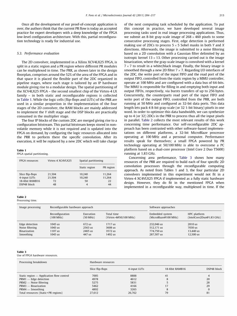
5.3. Performance evaluation
The 2D convolver, implemented in a Xilinx XCV4LX25 FPGA, issplit in a static region and a PR region where different PR modulescan be multiplexed in time. The PRR, as shown later in the designfloorplan, comprises around the 52% of the area of the FPGA and inthat space it is placed the flexible part of the 2DC organized inpipeline stages, where each stage is tailored by an IP hardwaremodule giving rise to a modular design. The spatial partitioning ofthe XCV4LX25 FPGA – the second smallest chip of the Virtex-4 LXfamily – in both static and reconfigurable regions is collectedin Table 1. While the logic cells (flip-flops and LUTs) of the PRR areused in a similar proportion in the implementation of the fourstages of the 2D convolver, the RAM blocks are mainly addressedto implement the Y shift stage and the DSP blocks are practicallyconsumed in the multiplier stage.
The four IP blocks of the custom 2DC are merged giving rise to aconfiguration bitstream. This partial bitstream keeps stored in non-volatile memory while it is not required and is updated into theFPGA on demand, by configuring the logic resources allocated intothe PRR to perform there the specific convolution. After itsexecution, it will be replaced by a new 2DC which will take charge
Table 1FPGA spatial partitioning.
FPGA resources Virtex-4 XC4VLX25 Spatial partitioning
Static region PR region
Slice flip-flops 21,504 10,240 11,264
4-input LUTs 21,504 10,240 11,264
18-Kbit RAMB16 72 50 22
DSP48 block 48 4 44
Table 2Processing time.
Image processing Reconfigurable hardware approach
Reconfiguration
(100 MHz)
Execution
(50 MHz)
Total time
(Virtex-4@50/1
Edge detection 1045 us 672 us 1717 us
Noise filtering 1045 us 2563 us 3608 us
Binarization 1107 us 2465 us 3572 us
Smoothing 1045 us 447 us 1492 us
Table 3Use of FPGA hardware resources.
Processing breakdown Hardware resources
Slice flip-flops
Static region — Application flow control 7005
PRM1 — Edge detection 4978
PRM2 — Noise filtering 5275
PRM3 — Binarization 5462
PRM4 — Smoothing 4892
Total resources (Static+PR regions) 27,612
of the next computing task scheduled by the application. To putthis concept in practice, we have developed several imageprocessing tasks used in real image processing applications. Thus,we submit an 8-bit gray-scale image of 268�460 pixels to someconsecutive processing stages. First, edge detection is performedmaking use of 2DCs to process 5�5 Sobel masks in both Y and X
directions. Afterwards, the image is submitted to a noise filteringbased on a 2D convolution with a Gaussian filter delimited by anisotropic kernel 13�13. Other processing carried out is the imagebinarization, where the gray-scale image is convolved with a kernel7�7 to result in a white/black image. Finally, the binary image issmoothed through a new 2D filter 7�7. Regarding I/O interfaces ofthe 2DC, the write port of the input FIFO and the read port of theoutput FIFO, controlled from the static region by a MMU controller,operate at 100 MHz and are configured with a data bus of 64-bits.The MMU is responsible for filling in and emptying both input andoutput FIFOs, respectively, via bursts transfers of up to 256 bytes.Concurrently, the counterparts read port of the input FIFO andwrite port of the output FIFO, controlled from the PRR, are bothrunning at 50 MHz and configured as 32-bit data ports. This datalength lets pack 4 8-bit gray-scale (or 32 1-bit binary) pixels in oneword. In order to optimize this data bandwidth, we can synthesizeup to 4 (or 32) 2DCs in the PRR to process thus all the input pixelsin parallel. Table 2 collects the most relevant results of this workconcerning time performance. Our self-reconfigurable 2DC ap-proach has been contrasted with other software-based implemen-tations on different platforms, a 32-bit MicroBlaze processoroperating at 100 MHz and a personal computer. Performanceresults speak for themselves; a small FPGA powered by PRtechnology operating at 50/100 MHz is able to overcome a PCplatform based on a dual-core processor (Intel Core 2 Duo T5600)running at 1.83 GHz.
Concerning area performance, Table 3 shows how manyresources of the PRR are required to build each of four specific 2Dconvolution processors through the reconfigurable computingapproach. As noted from Tables 1 and 3, the four particular 2Dconvolvers implemented in this experiment would not fit in aVirtex-4 XC4VLX25 FPGA if implemented as a fully static hardwaredesign. However, they do fit in the mentioned FPGA whenimplemented in a reconfigurable way, multiplexed in time. If the
Software approaches
00 MHz)
Embedded system
(MicroBlaze@100 MHz)
HPC platform
([email protected] GHz)
232,046 us 2810 us
512,171 us 7030 us
774,750 us 13,440 us
287,507 us 12,500 us
4-input LUTs 18-Kbit RAMB16 DSP48 block
8888 41 4
4612 8 20
5831 5 28
4166 17 29
3265 8 0
26,762 79 81

Table 4Hardware implementation features.
Image
processing
J� I Kernel
(pixels)
Kji Word
(bits)
pji Word
(bits)
Partial
bitstream
(bytes)
Edge detection 5�5 3 8 417,792
Noise filtering 13�13 18 8 417,792
Binarization 7�7 16 8 442,368
Smoothing 7�7 1 1 417,792
y0-6y0-5
y0-4y0-3
y0-2y0-1
y0
y0+1
y0+2
y0+3
y0+4
y0+5
y0+6 x0-6
x0-5x0-4
x0-3x0-2
x0-1x0
x0+ 1x0+ 2
x0+ 3
x0+ 5x0+ 4
x0+ 6-0.02
0
0.02
0.04
0.06
0.08
0.1
0.12
Fig. 5. Isotropic filter Kj,i of kernel 13�13 with 28 common tap coefficients.
F. Fons et al. / Microelectronics Journal 42 (2011) 204–217214
four types of 2D convolvers are not required at the same time by aspecific image processing application but they are mutuallyexclusive processing tasks then our run-time reconfigurable solutionlets carry out the entire system implementation in this small device.Therefore, it is not necessary to choose a higher, more expensive andpower-hungry FPGA as in case of a purely static hardware approach.In this sense, our PR implementation lets reach a more cost-effectivesolution for such an image processor embedded system.
Other relevant information from this experiment is the size ofkernels and operands involved in each convolution, as well as thesize of the partial bitstreams downloaded into the PRR for each ofthese specific 2DC PRMs, shown in Table 4.
All the convolution operations are performed in integer data.While in hardware you can adjust the bit length of the operandsfor each specific mathematical operation, the same computationin software can only adjust the size of the operands to thestandard integer types, restricted typically to 8-bit (char), 16-bit(short), 32-bit (long) and 64-bit (long long) lengths. Theseoperations are performed in software more or less efficientlydepending on the word length of the processor and theperformance and optimization features of the software compilerused.
As an example of the 2D convolver implementation, next it isdescribed in detail one of the specific 2D convolvers developed inthis work, just the one used in the noise filtering computationbased on an isotropic filter. The filter is composed of a kernel13�13 defined by the following tap coefficients:
Kj;i ¼1
220
�1 �6 �23 �60 �117 �174 �199 �174 �117 �60 �23 �6 �1
�6 �40 �154 �406 �788 �1166 �1328 �1166 �788 �406 �154 �40 �6
�23 �154 �593 �1554 �3001 �4420 �5028 �4420 �3001 �1554 �593 �154 �23
�60 �406 �1554 �2008 �1652 2890 5430 2890 �1652 �2008 �1554 �406 �60
�117 �788 �3001 �1652 7597 25236 36619 25236 7597 �1652 �3001 �788 �117
�174 �1166 �4420 2890 25236 68372 92746 68372 25236 2890 �4420 �1166 �174
�199 �1328 �5028 5430 36619 92746 124739 92746 36619 5430 �5028 �1328 �199
�174 �1166 �4420 2890 25236 68372 92746 68372 25236 2890 �4420 �1166 �174
�117 �788 �3001 �1652 7597 25236 36619 25236 7597 �1652 �3001 �788 �117
�60 �406 �1554 �2008 �1652 2890 5430 2890 �1652 �2008 �1554 �406 �60
�23 �154 �593 �1554 �3001 �4420 �5028 �4420 �3001 �1554 �593 �154 �23
�6 �40 �154 �406 �788 �1166 �1328 �1166 �788 �406 �154 �40 �6
�1 �6 �23 �60 �117 �174 �199 �174 �117 �60 �23 �6 �1
2666666666666666666666666664
3777777777777777777777777775
The 13�13 constants Kj,i of the filter can be reduced to only 28tap Kq,p coefficients if all the pixels located in relative positionswith the same coefficient are pre-added first before the stage ofproducts. They are highlighted in bold in the matrix above. Thegraphical view of the filter is illustrated in Fig. 5.
The same convolution algorithm has been implementedfollowing two different approaches: a purely-SW implementationand a PR-HW/SW co-design. Code 1 shows the software approachimplementation.
The same processing algorithm implemented in hardware isshown in Fig. 6. The maximum X size of the image that can beprocessed with this design depends on the depth of the DPRAMused in the Y shift module. It was set to 512 pixels in this example.Regarding the maximum Y size of the image, there are norestrictions here since the Y shifter work as an endless circulararray. These processing images are stored in a huge DDR-SDRAMrepository so basically there are no restrictions concerningnumber of images that can be processed.
As deduced from Fig. 6, the flexibility of our approach can bereached by modifying certain features of the hardware modulesused. For instance, the 2D convolver customized to the isotropickernel 13�13 could be converted into a new 2DC of kernel 9�9 byonly removing one 32-bit DPRAM block and one MUX in the Y shiftstage, reducing the X shift matrices of shift registers from 13�13 to9�9, changing the new K coefficients by resizing and updating theKq,p LUT and so on. These modifications are performed by means ofminor changes in the VHDL code of the four IP modules.

Fig. 6. Example of image 2D convolution with an isotropic filter of kernel 13�13. Processing of 4 pixels in parallel into the PRR.
F. Fons et al. / Microelectronics Journal 42 (2011) 204–217 215
Both implementations have been executed in their respectiveplatforms and both systems reach the same logical results, that is,the same output image as a result of convolving certain inputimage with the isotropic filter detailed in Fig. 5. However, theprocessing time differs dramatically, as shown in Table 2. In thehardware approach, four consecutive pixels are convolved inparallel whereas in the software approach of Code 1 theconvolution processing loop (z) needs to be repeated for each ofthese four consecutive pixels. It is important to highlight here that
in the PR hardware approach, the reconfiguration time of each 2Dconvolver is a constant while the processing time is a function ofthe size of the image to be processed, i.e. the higher the image, thelonger the processing time. Therefore, the effective reconfigura-tion overhead decreases as long as the image size (and itsprocessing time) increases.
Regarding the PR approach, the spatial partitioning of the FPGAresources into a PR region and a static region as well as theresultant partial bitstream of each of the four 2D convolvers is

Code 1. Example of 2D convolution of a 13x13 isotropic filter implemented in software.
F. Fons et al. / Microelectronics Journal 42 (2011) 204–217216
depicted in Fig. 7. The PRR shapes a rectangle in the left down sideof the FPGA layout whereas the rest of resources constitute thestatic region.
6. Conclusions
Modern SRAM-based field programmable gate array (FPGA)devices powered by partial reconfiguration (PR) glitchless tech-nology emerge today as a firm candidate to replace general-purpose processors in many embedded application domains. Suchengineering fields increasingly demand a stringent real-timeresponse in processing complex and compute-intensive algo-rithms without neglecting its low-cost implementation target. Tothe innate acceleration potential delivered by classical FPGAsthanks to its parallelism, deployed in space along scalable 2D logicfabric and measured as a purely spatial metric, state-of-the-artPR-FPGAs incorporate now a new design parameter inspired inthe temporal aspect of the logic fabric usage, which lets measurethe implementation efficiency of an application not through twosimple metrics – logic resources in use on one side and executiontime on the other – but in terms of only one two-dimensionalmeasurable derived from them such as functional density. Thisnew metric gives an idea of how much those resources are used intime. Like this, the benefits of logic-level specialization reached byclassical FPGAs are extended now in PR-FPGAs: this technologyexploits the ability to self-reconfigure a portion of the device at run-time to deploy there new functionality, without influencing the restof resources that concurrently continue their operation unaffected.This technique, termed dynamic partial self-reconfiguration, brings
a new design abstraction level allowing the exploitation ofconfigurable resources not only in space but also in time.
Two-dimensional convolution is a basic primitive demanded inmany digital signal processing applications today. This workfocuses on the design of a flexible 2D convolver aimed atdelivering a universal solution able to self-adapt its features atrun-time and be used thus by different processing stages in thesame application. After reviewing the state-of-the-art regardingdesign of 2DCs, it is noted that the level of flexibility concededtoday to these processors is extremely poor. Our approach aims tofill up this gap through an innovative technology such as run-time partial reconfiguration. With that goal in mind, an adaptiveFPGA-based 2DC has been presented, composed of differentpipelined HW functional units, and placed in a PRR of the FPGA,giving rise to a linear implementation. By reconfiguring the logicresources of the PRR at run-time, the 2DC gets customized to aparticular digital signal processing, on the fly, residing inhardware only the specific circuitry required at that moment. Aset of HDL libraries has been developed, which enables theapplication designer to tailor off-line the different 2DCs needed ina particular application. This collection of 2DCs is then stored inthe application repository in the way of partial bitstreams, asillustrated in Fig. 7, to be finally downloaded into the PRR at anymoment during the execution, thus delivering a high level ofversatility to the application while implementing it as a low-costembedded solution. The system gets composed of a small FPGAresponsible for performing the convolution operation and a largeexternal memory for storing both bitstreams and processingimages. As far as authors know, after comparing our approachwith the state-of-the-art 2D convolution processors reported until

Fig. 7. Partial bitstreams of image processing stages involving different 2D convolution features. FPGA floorplan and partitioning into static and PR regions.
F. Fons et al. / Microelectronics Journal 42 (2011) 204–217 217
today in the scientific literature, this work exploits the highestlevel of adaptability ever reached in 2D convolver designs at lowcost. Therefore, run-time partial reconfiguration technologydefinitely offers a competitive advantage in the design of adaptiveimage processors.
References
[1] E. Jamro, K. Wiatr, in: Dynamic constant Coefficient Convolvers Implementedin FPGAs, LNCS 2438, Springer, 2002, pp. 1110–1113.
[2] A.G.M. Strollo, et al., A reconfigurable 2D convolver for real-time SAR imaging,IEEE Conference on Electronics, Circuits & Systems (2001) 741–744.
[3] B. Bosi, et al., Reconfigurable pipelined 2-D convolvers for fast digital signalprocessing, IEEE Transactions on Very Large Scale Integration (VLSI) Systems 7(3) (1999) 299–308.
[4] S. Perri, P. Corsonello, VLSI implementations of efficient isotropic flexible 2Dconvolvers, IET Circuits Devices and Systems (2007) 263–269.
[5] S. Perri et al., SIMD 2-D convolver for fast FPGA-based image and videoprocessors, Conference on Military and Aero-space Prog. Logic Devices, 2003.
[6] S. Perri, et al., A high-performance fully reconfigurable FPGA-based 2Dconvolution processor, Microprocessors and Microsystems, Elsevier (2005)381–391.
[7] V. Sriram, D. Kearney, A FPGA implementation of variable kernel convolution,in: Proceedings of the IEEE Conference on Parallel and Distributed Computing,Applications and Technologies, 2007, pp. 105–109.
[8] M.J. Wirthlin, B.L. Hutchings, Improving functional density using run-timecircuit reconfiguration, IEEE Transactions on Very Large Scale Integration(VLSI) Systems 6 (2) (1998) 247–256.