rf power circuit designs for wi-fi applications
TRANSCRIPT

University of South Florida University of South Florida
Scholar Commons Scholar Commons
Graduate Theses and Dissertations Graduate School
June 2019
RF Power Circuit Designs for Wi-Fi Applications RF Power Circuit Designs for Wi-Fi Applications
Krishna Manasa Gollapudi University of South Florida, [email protected]
Follow this and additional works at: https://scholarcommons.usf.edu/etd
Part of the Electrical and Computer Engineering Commons
Scholar Commons Citation Scholar Commons Citation Gollapudi, Krishna Manasa, "RF Power Circuit Designs for Wi-Fi Applications" (2019). Graduate Theses and Dissertations. https://scholarcommons.usf.edu/etd/8362
This Thesis is brought to you for free and open access by the Graduate School at Scholar Commons. It has been accepted for inclusion in Graduate Theses and Dissertations by an authorized administrator of Scholar Commons. For more information, please contact [email protected].

RF Power Circuit Designs for Wi-Fi Applications
by
Krishna Manasa Gollapudi
A thesis submitted in partial fulfillment
of the requirements for the degree of
Master of Science in Electrical Engineering
Department of Electrical Engineering
College of Engineering
University of South Florida
Major Professor: Stephen E. Saddow, Ph.D.
Gokhan Mumcu, Ph.D.
Jing Wang, Ph.D.
Date of Approval:
June 12, 2019
Keywords: Wireless communications, repeaters, power combiners, Wilkinson divider, isolation
losses
Copyright © 2019, Krishna Manasa Gollapudi

DEDICATION
This thesis is dedicated to my parents who taught me to achieve anything step by step and
helped me thrive. My sister who constantly urged me to give my best and my brother who has
always had my back.

ACKNOWLEDGEMENTS
I would like to thank my advisor Dr. Stephen E. Saddow who guided me throughout this
research from inception. I want to express my gratitude to Dr. Gokhan Mumcu and Dr. Jing Wang
for their input and patience. I am deeply grateful for my Senior Engineer, Steven Chung for
providing me an opportunity of working as an intern at Global ETS, LLC. I feel blessed to have
learnt Microwave and RF courses from the Department of Electrical Engineering and helped me
pave the path of success.

i
TABLE OF CONTENTS
LIST OF TABLES iii
LIST OF FIGURES iv
ABSTRACT viii
CHAPTER 1: INTRODUCTION 1
1.1 Motivation 1
1.2 Wireless Communication 2
1.2.1 Performance of Wireless Transmitters and IEEE Standards 4
1.2.2 Radio Frequency Transceivers 6
1.2.3 Repeaters 8
1.3 Objectives and Scope of the Thesis 10
1.4 Thesis Outline 10
CHAPTER 2: THEORY OF POWER DIVIDERS 12
2.1 S Parameter Matrix 12
2.2 Types of Power Dividers 15
2.2.1 Wilkinson’s Power Divider 19
2.3 Even and Odd Mode Analysis on Wilkinson Divider 21
2.3.1 Even Mode Analysis of Wilkinson’s Divider 23
2.3.2 Odd Mode Analysis of Wilkinson’s Divider 24
CHAPTER 3: RF TRANSISTORS TESTING 28
3.1 RF Transistor Validation 28
3.1.1 RF Amplifiers 29
3.2 Amplifier Boards Designed at Global ETS, LLC 32
3.2.1 Qorvo SGA 3263Z Amplifier 32
3.2.2 Qorvo SGA 5586Z Amplifier 38
3.2.3 Qorvo AG303-86 Amplifier 40
CHAPTER 4: DESIGN AND FABRICATION 45
4.1 Microstrip Transmission Lines and Dimensions 45
4.2 Ideal Design of Wilkinson Power Divider and Expected Performance 47
4.3 Design and Simulated Results of Wilkinson’s Power Divider 49
4.3.1 Design and Construction of Curved Wilkinson Divider
with Step Junction 50
4.3.2 Wilkinson Divider with Continuous Taper 52
4.3.3 Wilkinson’s Divider Design using Co-simulation 55
4.3.4 Layouts of Power Divider Circuits 58
4.4 Construction and Results 58

ii
CHAPTER 5: CONCLUSION AND FUTURE SCOPE 70
5.1 Conclusions 70
5.2 Future Work 73
5.2.1 Applications of Power Dividers in the RF and Microwave Industry 73
5.2.2 Possible Power Divider Improvements 75
REFERENCES 77

iii
LIST OF TABLES
Table 1 Evolution of IEEE Wi-Fi Standards 5
Table 2 Isolation and Insertion Losses for Number of Output Ports 21
Table 3 Port Voltages of Odd Mode and Even Mode Analysis of Wilkinson’s
Divider 25
Table 4 Voltages at Each Port of Power Divider 26
Table 5 Types of Amplifiers and Their Properties 32
Table 6 Parameter Specifications of SGA 3263Z Amplifier 34
Table 7 Measured vs Simulated Parameters of SGA 3263Z 37
Table 8 Desired Specifications Given in Manufacturer’s Datasheet 39
Table 9 Desired Specifications vs Simulated Parameters 40
Table 10 Gain (dB) vs Frequencies (MHz) AG303-86 Amplifier 44
Table 11 Specifications and Values of the Chosen FR4 Substrate 47
Table 12 Commercial Wilkinson’s Power Divider Specifications 49
Table 13 Comparison of Measured and Simulated Return Losses at 2.4 GHz 67
Table 14 Insertion Losses of Measured and Simulated Power Dividers at 2.4 GHz 68
Table 15 Comparison Between the Measured and Simulated Isolation of
Power Dividers 69

iv
LIST OF FIGURES
Figure 1 Block Diagram of Basic Transceiver System 6
Figure 2 Schematic Diagram of Transmitter Circuit 7
Figure 3 Schematic Diagram of Receiver Circuit 8
Figure 4 Mobile Communication Coverage Using a Wireless Repeater 9
Figure 5 Power Divider and Power Splitter Schematics 16
Figure 6 Lossless T Junction Power Divider Schematic 16
Figure 7 Three Port Resistive Divider Schematic 17
Figure 8 Transmission Line Model of Wilkinson Power Divider 19
Figure 9 Schematic of the Divider with Source at Port 2 22
Figure 10 Wilkinson Divider with Source Voltages at Ports 2 and 3 and the Load at
Port 1 (i.e., Using the Wilkinson Divider as a Power Combiner) 22
Figure 11 Even Mode Wilkinson Schematic Circuit with Virtual Open 23
Figure 12a Half Circuit of Even Mode Wilkinson Divider 24
Figure 12b Simplified Even Mode Circuit 24
Figure 13 Equivalent Circuit of the Odd Mode Wilkinson’s Divider 25
Figure 14 Simple Block Diagram of Transceiver Circuit 30
Figure 15 Transmission System Employing Different Amplifier Types as Shown (LNA,
PA, Driver, etc.) 31
Figure 16 Receiver System Employing Different Amplifier Types as Shown (LNA,
PA, Driver, etc.) 32
Figure 17 Transmission Pin Diagram of Qorvo SGA 3263Z RF Transistor 33
Figure 18 Schematic Diagram of SGA 3263Z Amplifier Board 34

v
Figure 19 Fabricated PCB of SGA 3263Z from Global ETS, LLC 35
Figure 20a Gain (S21) dB of the Amplifier Board of Figure 19 35
Figure 20b Input Return Loss (S11) of the Amplifier Board 36
Figure 20c Output Return Loss (S22) of the Amplifier Board 36
Figure 20d Noise Figure Measurement Setup of the Amplifier Board 36
Figure 20e OIP3 Power at 8520 MHz 37
Figure 20f OIP3 Extrapolated Value at 1950 MHz 37
Figure 21 Pin Diagram of SGA5586Z HBT Transistor Darlington Pair 38
Figure 22 Schematic Diagram of SGA 5586Z Amplifier Board 39
Figure 23 Simulated S-parameters of SGA 5586Z Amplifier Board 40
Figure 24 Pin Diagram of AG303-86 Transistor 41
Figure 25 Schematic Diagram of the Amplifier Board 41
Figure 26 RF Test Socket on the PCB to Test Each of 6000 RFMD AG303-86
InGaP HBTs 42
Figure 27 Layout of AG303-86G Amplifier Board 43
Figure 28 Assembled Board of the Amplifier Containing the TriQuint AG303-86 43
Figure 29 Measured Gain of the TriQuint AG303-86G InGaP HBT Amplifier Board
from 300 MHz to 2 GHz. 44
Figure 30 Microstrip Transmission Line on a Substrate with Relative
Permittivity ℇr
46
Figure 31 Ideal Schematic Circuit of Wilkinson’s Power Divider to be Fabricated
on FR4 Substrate Board 48
Figure 32 Simulated Results of Wilkinson’s Power Divider Using the Circuit Design 48
Figure 33 Schematic Diagram of Curved Power Divider with Step Junction 50
Figure 34a Simulated Input Return Loss (S11) and Output Return Loss (S22, S33) in
dB of Design 1 51

vi
Figure 34b Simulated Isolation between the Output Ports 2 and 3 (S32, S23) in dB
vs F (GHz) of Design 1 51
Figure 34c Simulated Insertion Losses (S21, S31) in dB vs F(GHz) of Design 1 51
Figure 35 Schematic Diagram of a Power Divider Circuit with Tapered Junction
Between the 50Ω and 70.71Ω Transmission Lines 53
Figure 36a Simulated Input and Output Return Losses (S11, S22 and S33) in dB of
Design 2 53
Figure 36b Simulated Insertion Losses (S12, S13) in dB of Design 2 54
Figure 36c Simulated Isolation between the Output Ports in dB (S32, S23) of
Design 2 54
Figure 37 Circuit Schematic of Straight Power Divider 55
Figure 38 Layout of Straight Power Divider Using Co-simulation Method 56
Figure 39 Substrate Dimensions for Performing EM Simulation on Straight
Power Divider 56
Figure 40 Circuit Layout Created Using Co-sim Method Using the Straight Power
Divider Symbol 56
Figure 41a Insertion Losses in dB vs F (GHz) of Design 3 57
Figure 41b Simulated Design 3 Input and Output Return Losses 57
Figure 41c Simulated Design 3 Isolation 57
Figure 42a, b Step and Tapered Junction Power Dividers 58
Figure 42c Straight Power Divider 58
Figure 43 Photographs of the Milled Wilkinson Power Dividers with (a) Step
Junction, (b) Taper Junction and (c) Straight Dividers 59
Figure 44a Input Return Loss (S11), Output Return Loss of Port 2 (S22) and Insertion
Loss of Port 2 (S21) vs F (GHz) of Design 1 59
Figure 44b Insertion Loss of Port 3 (S31) vs F (GHz) of Design 1 60
Figure 44c Output Return Loss of Port 3 (S33) vs F (GHz) of Design 1 60
Figure 45a Input Return Loss (S11), Output Return Loss of Port 2 (S22) and Insertion
Loss of Port 2 (S21) vs F (GHz) of Design 2 61
vii
Figure 45b Insertion Loss of Port 3 (S31) vs F (GHz) of Design 2 61
Figure 45c Output Return Loss of Port 3 (S33) vs F (GHz) of Design 2 62
Figure 46a Input Return Loss (S11), Output Return Loss (S22) and Insertion Loss
(S21) vs F (GHz) of Design 3 63
Figure 46b Insertion Loss of Port 3 (S31) vs F (GHz) of Design 3 63
Figure 46c Output Return Loss of Port 3 (S33) vs F (GHz) of Design 3 64
Figure 47a Isolation (S23) Between the Output Ports 2 and 3 (in dB) vs F (GHz) of
Design 1 65
Figure 47b Isolation (S23) Between the Output Ports 2 and 3 (in dB) vs F (GHz) of
Design 2 65
Figure 47c Isolation (S23) Between the Output Ports 2 and 3 (in dB) vs F (GHz) of
Design 3 66
Figure 48 Block Diagram of N-way Power Divider used as a Feed Network 74
Figure 49 Power Combiner/Divider in a Wi-Fi Transceiver Circuit to Boost the Wi-Fi
Signals and to Establish the Wi-Fi Link when the Transmitter/Receiver
are Mobile 75
Figure 50 The Layout of a Typical Rat Race Coupler 76

viii
ABSTRACT
In the field of RF/Microwave Engineering, the Wilkinson Power divider is a passive device
frequently used for splitting or combining signals. The power fed to the input port is equally or
unequally split between N output ports and delivers better performance by achieving isolation
between the output ports while matching all the ports. The design comprises simple transmission
lines and provides power divider characteristics with the help of quarter wavelength transmission
lines with different topologies.
This thesis describes the design and fabrication of lumped and N way power splitter
working at an operating frequency of 2.4 GHz. These circuits are designed with Advanced Design
System Software (ADS) by adopting novel Wilkinson’s Power Splitter/ combiner design and are
fabricated using microstrip fabrication techniques. The objective of this thesis it to design a 2-way
power divider with different topologies and thoroughly compare the microstrip layout impact on
isolation and return losses.
1
CHAPTER 1
INTRODUCTION
1.1 Motivation
Power dividers played a prominent role in the field of microwaves for many years and their
basic function is to combine or divide the power entering the input port into N output ports as
required. Some of the applications of these dividers are parallel distribution of low power signals
into antenna arrays and to measure the intermodulation distortions with appropriate phase
relationship to combine signals from a source as a combiner [1] and in transceiver systems to
provide the local oscillator signal to both the transmitter and receiver circuits. Power dividers are
generally thought of as microwave equipment, and typically constructed with an equivalent
impedance of 50Ω at each port. Power is divided equally between the ports from a uniform
transmission line feed. They ideally provide a good impedance match at both the output ports when
the input is terminated with the network’s characteristic impedance, usually 50Ω. After achieving
an optimum impedance match to the source feed, a power divider is used to split the input into
equal signals for comparison measurements. Since power dividers are bi-directional, they can also
be used as power combiners. Dividers are also used to measure different characteristics of signals
like frequency and power for broadband signal sampling.
The objective of this thesis is to design, fabricate and analyze the performance of a two-
way power divider for Wi-Fi applications. This design selected was adopted from Wilkinson’s
novel design of power combiners, working with an operating frequency of 2.4 GHz since the IEEE
Wi-Fi standard IEEE 802.11 operates at this frequency [2]. Advanced Design System™ software

2
from Agilent was used as a tool in designing the circuit schematic and corresponding layout.
Scattering parameter matrices for the device were studied and analyzed to draw conclusions about
the dependency of the isolation and return losses on the microstrip layout of the circuits. It was
typically claimed that the straight, parallel quarter wavelength transmission lines exhibit
degradations in isolation when compared to curved quarter wavelength transmission lines when
ignoring the effect of coupling between the quarter wavelength transmission lines. A thorough
study on these designs was performed to determine the effects of designs on isolation and return
loses.
The inspiration for this thesis was the application of power combiner/divider circuits in
wireless communication systems to improve the wireless signals (Wi-Fi signals) in a transceiver
system. Since there are places where the wireless signals cannot reach, such as outdoor areas, large
office spaces, etc. wireless repeater circuits are required. The technology for radio frequency
wireless local area networking is called Wi-Fi and is based on the IEEE 802.11 standard.
1.2 Wireless Communication
Wireless communication is the transfer of data or power between two or more points, that
are not connected through a wire. Simply, wireless communication is the data communication
performed wirelessly [3]. Usually, wireless technologies employ radio waves as the means of
communication. This is due to their ability to travel millions of kilometers for deep space radio
communications or few meters for Bluetooth applications. Different types of fixed, mobile or
portable applications like cellular phones, two-way radios, wireless computer mice and keyboards,
etc., are enclosed by wireless communications. This term was first used in 1890 for radio
transmitting and receiving technology as in wireless telegraphy until it was replaced by radio in
the 1920s [4][5]. Due to the emergence of broadband communication, Wi-Fi and Bluetooth, the
term wireless became the primary usage in the 2000s. In the telecommunications industry, wireless
3
operation permit services such as long-range communications, that are impossible to achieve using
wires by employing radio transmitters, receivers, and remote controls by using energy to transfer
the data without using the wires over short and longer distances [6]
A wireless network can refer to a computer network that uses wireless data connections
between network nodes, which is either a redistribution point or a communication endpoint in
telecommunication systems. Wireless telecommunications are implemented using radio waves as
a form of communication called radio communication. Some of the examples of wireless networks
include cellular phone networks, wireless Local Area Networks, wireless sensor networks and
terrestrial microwave networks, the networks which uses earth-based transmitters and receivers in
low frequency range [7].
Wireless PAN (Wireless Personal Area Network), Wireless LAN (Wireless Local Area
Network), Wireless MAN (Wireless Metropolitan Area Networks), and Wireless WAN (Wireless
Wide Area Network) are some of the wireless networks.
• Wireless PAN: This is a personal network, that connects the devices in smaller areas within
a person’s reach. The applications like Bluetooth and ZigBee are popular for these
networks.
• Wireless LAN: Wireless local Area networks link two or more devices using a wireless
distribution method over shorter distances, providing internet access through access points.
• Wireless MAN: When several Wireless LANs are connected, the wireless network is called
a Wireless Metropolitan Area Networks. The IEEE standard for one of the Wireless MAN
i.e. WiMAX is 802.16 [8].
• Wireless WAN: These networks cover large areas and can be used to connect to branch
offices of businesses [9] or provide internet access to public systems. The wireless
4
connections between these access points are usually microwave links using parabolic
dishes in the 2.4 GHz and 5.8 GHz bands.
Employing radio waves is the most common method of transferring information wirelessly.
Wireless communication is achieved by generating and then transmitting electromagnetic waves
and then receiving these waves at a remote destination through the air at the speed of light. Since
the radio signal wavelength is the proportional to frequency, shorter wavelength corresponds to
higher frequencies. Usually, radio waves are measured in cycles per second with the common
designation of Hertz (Hz for short). Hence, signal travel at great distances typically uses longer
wavelengths and the penetration of longer wavelength signals through, and around, objects are
better than shorter wavelength signals. Indeed, short wavelength radio communication is referred
to as ‘line of sight’ for this reason since any obstruction (trees, buildings, etc.) greatly degrade the
power transmitted to the remote receiver. This process of transmitting and receiving radio signals
through wireless networks involves RF devices, principally a transmitter and receiver. These
devices are often combined into a signal piece of RF gear and called transceivers when in a single
package. Usually one of these devices is silenced while the other functions. For example, in a radio
transceiver, the transmitter is silenced while receiving the signals so as not to saturate the receiver,
etc.
1.2.1 Performance of Wireless Transmitters and IEEE Standards
Wi-Fi stands for wireless fidelity and is a specific method to connect users, such as
computers, tablets, smart phones, etc., to the internet, according to the IEEE’s set of wireless
standards. These standards describe the set of services and protocols followed by the Wi-Fi
transmission networks. The most commonly encountered set of standards is IEEE Standard 802.11
wireless LAN (WLAN) and mesh. This family of specifications initially started in the 1990s and
continues to evolve. These standards specify the improvements that boost wireless range and

5
addresses technologies that reduce power consumption. Amendments introduced during the
evolution of the standards include 802.11 n, 802.11 ac and 802.11 ax, which support higher data
rates by adopting higher-order modulation schemes. To maintain higher data rates, attempts were
made to improve the spectral efficiency and multi-user techniques like MU-MIMO and OFDMA
which have been introduced to improve network capacity and spectral frequencies (bits of data
transmitted per second through 1 Hz of RF spectrum). The following table summarizes the IEEE
standards from obsolete to newer amendments:
Table 1: Evolution of IEEE Wi-Fi Standards [3], [9]
Specification 802.11a 802.11b 802.11g 802.11n 802.11ac 802.11ax
Year released 1999 1999 2003 2009 2014
Expected in
2019
Operating Band
2.4
GHz
5
GHz
2.4
GHz
2.4 and 5
GHz
5
GHz
2.4 and 5
GHz
Channel
Bandwidth
20
MHz
20
MHz
20
MHZ
20/40
MHz
20/40/80/160
MHz
20/40/80/160
MHz
Physical Layer
rate
11
Mbps
54
Mbps
54
Mbps
600
Mbps
6.8
Gbps
10
Gbps
Link Spectral
Efficiency
0.55
bps/Hz
2.7
bps/Hz
2.7
bps/Hz
15
bps/Hz
42.5
bps/Hz
65.5
bps/Hz
The operational range of wireless signals depends on factors like frequency band,
sensitivity of receiver, antenna choice (transmitter and receiver) and modulation technique.
Additionally, propagation characteristics of signals have a strong impact on their strength. At large

6
distances and with greater signal absorption, signal speed is usually reduced. Generally, the
maximum power that a Wi-Fi device can transmit is limited by local regulations like such as the
Federal Communications Commission (FCC) in the United States and Equivalent isotropically
radiated power in the European Union limit the maximum power to 20 dBm or 100 mW [3].
1.2.2 Radio Frequency Transceivers
A typical wireless transceiver has a transmitter circuit which transmits the data in the form
of radio signals and a receiver circuit. The communication system consists of a transmitting and
receiving antenna to transmit and receive radio signals, respectively, low noise amplifiers (LNAs)
to boost the received signals while maintaining a constant signal to noise ratio (SNR), filters to
remove undesired signals, mixers and local oscillators to up/down convert the signals and power
amplifiers (PAs) to amplify these signals and transmit them. The block diagram of an RF
transceiver system is shown in Figure 1.
Figure 1: Block Diagram of Basic Transceiver System.
The VCO feeds the transmitter (bottom) and receiver (top) circuits. The antenna is both
transmit/receive and the SPDT switches between transmit mode (connecting bottom path to the
antenna) and receive mode (connecting the top path to the antenna).
7
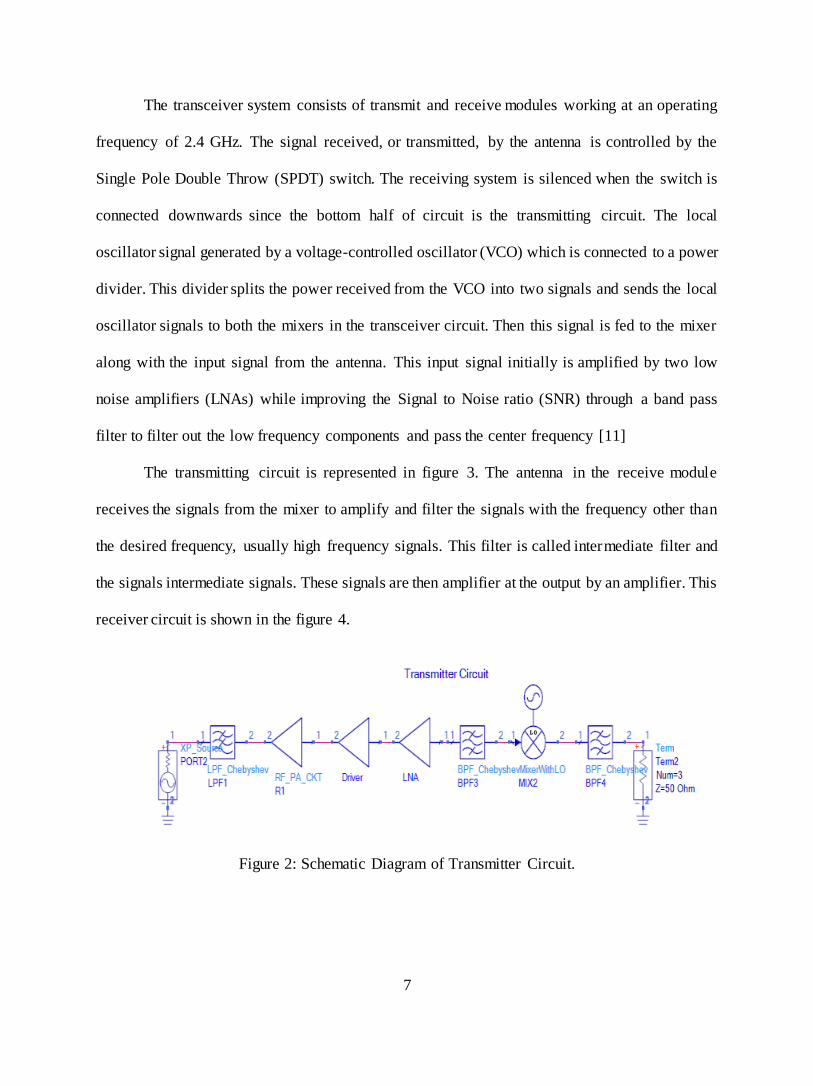
The transceiver system consists of transmit and receive modules working at an operating
frequency of 2.4 GHz. The signal received, or transmitted, by the antenna is controlled by the
Single Pole Double Throw (SPDT) switch. The receiving system is silenced when the switch is
connected downwards since the bottom half of circuit is the transmitting circuit. The local
oscillator signal generated by a voltage-controlled oscillator (VCO) which is connected to a power
divider. This divider splits the power received from the VCO into two signals and sends the local
oscillator signals to both the mixers in the transceiver circuit. Then this signal is fed to the mixer
along with the input signal from the antenna. This input signal initially is amplified by two low
noise amplifiers (LNAs) while improving the Signal to Noise ratio (SNR) through a band pass
filter to filter out the low frequency components and pass the center frequency [11]
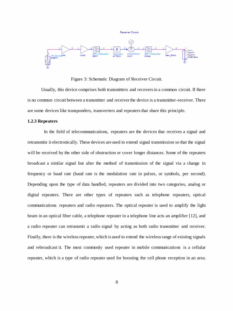
The transmitting circuit is represented in figure 3. The antenna in the receive module
receives the signals from the mixer to amplify and filter the signals with the frequency other than
the desired frequency, usually high frequency signals. This filter is called intermediate filter and
the signals intermediate signals. These signals are then amplifier at the output by an amplifier. This
receiver circuit is shown in the figure 4.
Figure 2: Schematic Diagram of Transmitter Circuit.
8
Figure 3: Schematic Diagram of Receiver Circuit.
Usually, this device comprises both transmitters and recovers in a common circuit. If there
is no common circuit between a transmitter and receiver the device is a transmitter-receiver. There
are some devices like transponders, transverters and repeaters that share this principle.
1.2.3 Repeaters
In the field of telecommunications, repeaters are the devices that receives a signal and
retransmits it electronically. These devices are used to extend signal transmission so that the signal
will be received by the other side of obstruction or cover longer distances. Some of the repeaters
broadcast a similar signal but alter the method of transmission of the signal via a change in
frequency or baud rate (baud rate is the modulation rate in pulses, or symbols, per second).
Depending upon the type of data handled, repeaters are divided into two categories, analog or
digital repeaters. There are other types of repeaters such as telephone repeaters, optical
communications repeaters and radio repeaters. The optical repeater is used to amplify the light
beam in an optical fiber cable, a telephone repeater in a telephone line acts an amplifier [12], and
a radio repeater can retransmit a radio signal by acting as both radio transmitter and receiver.
Finally, there is the wireless repeater, which is used to extend the wireless range of existing signals
and rebroadcast it. The most commonly used repeater in mobile communications is a cellular
repeater, which is a type of radio repeater used for boosting the cell phone reception in an area.
9
Usually cellular repeaters have a directional antenna to receive the signals from the tower, an
amplifier to boost the signal which is then rebroadcast to nearby cellphones using a local antenna.
The communication coverage is improved by radio repeaters and, without a repeater, these
systems have limited range due to land terrain and obstructions. Similarly, to boost or to extend
the range of Wi-Fi signals wireless repeaters are often deployed. This circuit operates by taking a
signal from a wireless router, or from an access point and rebroadcasting it to create a secondary
network. Wireless repeaters are usually used when two or more users must be connected over
longer distances when direct connection cannot be established commonly in homes and offices.
These repeaters are usually employed in an environment where interference exists due to
environmental factors like the presence of microwaves from the microwave oven or from the
metals or from computer devices or hubs [3]. The absence of a wireless hotspot can also be one of
the reasons to employ wireless repeater.
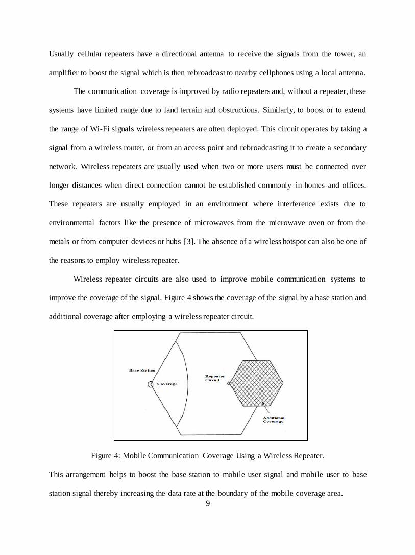
Wireless repeater circuits are also used to improve mobile communication systems to
improve the coverage of the signal. Figure 4 shows the coverage of the signal by a base station and
additional coverage after employing a wireless repeater circuit.
Figure 4: Mobile Communication Coverage Using a Wireless Repeater.
This arrangement helps to boost the base station to mobile user signal and mobile user to base
station signal thereby increasing the data rate at the boundary of the mobile coverage area.

10
1.3 Objectives and Scope of the Thesis
The objective of this thesis is to design a wireless repeater circuit to boost signals on an as-
needed basis. This was accomplished via n-way Wilkinson power divider circuits, with different
topologies implemented using Advanced Design System (ADS) software. These circuits can have
different layout configurations such as bent, curved and tapered designs. After constructing the
divider circuits, they were further analyzed, and compared.
The scope of the thesis is:
• A Literature review of S-parameter matrices and different power-dividing circuit designs
• Selection of suitable power dividers
• Design of Wilkinson power Divider (3 Port) using ADS
• Comparison of the different design topologies for different Wilkinson power dividers
• Fabrication of prototype power dividers using FR4 as substrate board
• Measurement of prototype device performance with a Vector Network Analyzer
• Analysis and comparison between simulated and fabricated Wilkinson power dividers
1.4 Thesis Outline
This thesis is organized into 5 chapters. Chapter 2 covers even and odd mode circuit
analysis of the Wilkinson power divider to help in understanding the performance and their
corresponding S-matrices. RF devices, types of amplifiers and their design methodology,
fabrication and testing methods as a part of internship experience at an electronics company,
Global ETS, LLC (Odessa, FL) is discussed in Chapter 3. Chapter 4 presents the design procedure
and construction methods of the dividers using Advanced Design System software. The ideal
Wilkinson power divider and its performance with simple simulations are also included to help
understand the limitations of this device. The design of a 2-way Wilkinson divider (with straight
and bent topologies) are also included in this chapter. Finally, validation of the simulated results

11
obtained in previous chapters along with a brief discussion of conclusions drawn from this research
and their potential future work are presented in chapters 4 and 5.

12
CHAPTER 2
THEORY OF POWER DIVIDERS
Power combiners couple definite amount of power in a transmission line to a port, allowing
the signal to be used in another circuit. A scattering matrix helps in quantifying the electromagnetic
energy propagating through a multiport network. For an RF signal incident at one port, some
fraction of the power is reflected, and some enters the incident port and then scatters through all
the ports. The representation of the possible input and output path of the signal in a mathematical
construct is in matrix format as a scattering matrix or S-matrix. Each parameter in the matrix is a
complex number, having magnitude and phase or real and imaginary parts. The rows and columns
depend on the number of the ports the network has and is discussed further in this chapter.
2.1 S Parameter Matrix
Before considering the different types of power dividers commonly used in the RF
industry, a better understanding of the scattering matrix (S-matrix) is required. This matrix is
typically used to relate the total voltages and currents at the RF circuit ports by considering both
signal magnitude and phase. Thus S-parameters provides a complete description of an N-port RF
network at microwave frequencies. The S-matrix for an arbitrary N-port microwave network is
written with V- indicating the amplitude of reflected voltage waves from port n and V+ indicating
the amplitude of the incident voltage waves to port n as (1-4):
[𝑉1
−
⋮𝑉𝑛
−] = [
𝑆11 ⋯ 𝑆1𝑛
⋮ ⋱ ⋮𝑆𝑛1 ⋯ 𝑆𝑛𝑛
] [𝑉1
+
⋮𝑉𝑛
+] (2.1)
Each element in the matrix can be determined using:

13
𝑆𝑖𝑗 = 𝑉𝑖
−
𝑉𝑗+ (2.2)
where 𝑉𝑗+ is the reflected voltage wave exiting through port “i” and 𝑉𝑖
− is the incident voltage
wave entering through port “j”. Specifically, this is the ratio of an incident wave incident on port j
and a reflected wave exiting through port i. Usually, a Vector Network Analyzer (VNA) is used to
measure the S parameters by considering that all the incident waves on all the ports except port j
are zero. For some devices that have more than two ports, such as splitters, which usually have
three, any port which is not used for measurement is terminated with a matched load. It is known
that if the device is matched at all the ports the input impedance of each port is equal to the total
characteristic impedance of the system, resulting in zero reflection coefficient. This means that the
wave incident on the matched port will not be reflected as the reflected voltage is zero. If the
matched port condition (where i=j) is applied to the s-matrix, the diagonal elements will be reduced
to zero.
In principle power dividers are reciprocal in performance. Reciprocity is the property
exhibited when the transmission of power in a device or circuit between two ports which is the
same irrespective of direction of propagation through the device. Hence the equation can be
represented as
𝑆𝑖𝑗= 𝑆𝑗𝑖 (2.3)
The S-matrix elements for a reciprocal device, make the matrix symmetrical, is used to
determine the losses induced by the device itself. Ideally, a lossless power divider is desired, but
we can practically realize only a low-loss divider. It is proven that the device would be lossless if
the elements in the S-matrix are unitary, which means that the sum of squares of elements in the
rows equals one. This can be represented in product form as
[𝑆]t [𝑆]* = [𝐼] (2.4)

14
where [𝐼] represents a unit matrix. [𝑆]t is the transpose and [𝑆]* is the conjugate of S- matrix [13].
Hence, if any device follows the above condition, it is a lossless device.
The performance of a power divider can also be influenced by the isolation between output
ports of the device. Isolation is the property of a device where a signal at one port does not affect
the signal from another port. Usually, for a three-port power divider, to reduce the interference
caused by coupling between the ports, it is necessary for the output ports to be isolated. In a power
divider circuit, if port 2 and port 3 are output ports, the elements 𝑆32 and 𝑆23 relate to port isolation.
These are the ports where a signal enters through port 3 and exits through 2, and vice versa. Since
we need strong isolation between these ports, their magnitudes should be small.
The ideal power divider should be lossless, reciprocal, and matched at all the ports.
However, it is not possible to have a lossless divider with matched ports under all conditions. To
denote this, we can consider a general S-matrix as:
[𝑆] = [𝑆11 𝑆12 𝑆13
𝑆21 𝑆21 𝑆23
𝑆31 𝑆32 𝑆33
] (2.5)
Assume that the device is matched and reciprocal. By applying all the conditions mentioned above
to the general s-matrix, it is modified as:
[𝑆] = [0 𝑆12 𝑆13
𝑆21 0 𝑆23
𝑆31 𝑆32 0] (2.6)
Now, to prove the matching condition, the s-matrix should be unitary as:
|𝑆12|2 + |𝑆13|2 = 1 (2.7)
|𝑆21|2 + |𝑆23|2 = 1. (2.8)
|𝑆31|2 + |𝑆32|2 = 1 (2.9)
𝑆23∗ 𝑆13 =1 (2.10)
𝑆13∗ 𝑆12 =1 (2.11)

15
𝑆23∗ 𝑆12 =1. (2.12)
To satisfy the above conditions, two of the three elements 𝑆13,𝑆12 and 𝑆23 should be zero
[15]. However, considering any two of these elements, all three conditions of lossless, reciprocal,
and matched are not satisfied. Hence, a Wilkinson’s power divider can be designed as a reciprocal
and a matched device, but it is lossy.
2.2 Types of Power Dividers
In many radio frequency and microwave applications, it is necessary to divide power
simultaneously to multiple circuits. This can be accomplished easily with power dividers and
splitters. The difference between a splitter and divider is the configuration of the resistor used in
dissipation of power in these circuits. While an ideal power divider with lossless, reciprocal, and
matched properties cannot be realized physically, there some power dividers which can follow two
of these properties. Some of the common power dividers like T junction dividers, resistive dividers,
and Wilkinson dividers, have unique design properties. Both the dividers and splitters can be
realized with quarter wave transformers, transmission lines, micro strip transmission lines or strip
lines. Power dividers and splitters are not interconvertible. A power divider can also be used as a
power combiner, acting as a bidirectional and symmetrical device. Common applications where a
divider acts a combiner are in communication receivers where power needs to be combined from
different sources and in amplifier circuits where power needs to be combined from different power
amplifiers. A simple power splitter and power divider having lumped components with two
resistors and three resistors, respectively, are shown in Figure 5.

16
Figure 5: Power Divider and Power Splitter Schematics.
Power dividers are usually N-port devices that are lossless or, as a minimum, low loss
devices. A basic three port (one input port and two output ports) device splits power equally (3
dB) into each output port. An unequal split power divider is also physically realizable. The design
specifications required for a power divider in most applications are high isolation, high return
losses, low insertion losses, compact size and high bandwidth.
A lossless T junction power divider can be simply designed as three transmission lines
intersecting at a junction, which has reactance due to fringing fields and higher order modes
corresponding to the discontinuity formed at a junction resulting in storage of energy caused by
the lumped susceptance, B. The lossless T junction divider is shown in Figure 7.
Figure 6: Lossless T Junction Power Divider Schematic.
(a) Power Divider. (b) Power Splitter.
17
The total impedance of this T junction divider is given by:
1
𝑍0 =
1
𝑍1 +
1
𝑍2 + jB (2.13)
In the above equation, 𝑍0 is the impedance of the input port and 𝑍1and, 𝑍2 are the impedances of
the output ports.
If B equals zero, we can rewrite the above equation as
1
𝑍0 =
1
𝑍1 +
1
𝑍2 (2.14)
However, if B is not negligible, we can reduce the effect of the susceptance by using a
reactive tuning element over a narrow frequency range. Since transmission lines have less losses,
the required impedances to obtain respective power ratios in each section can be determined [13].
Although the lossless T junction power divider can be reciprocal, it is not matched at all
ports. From the above-mentioned equation (2.14), we can deduce that it cannot be matched since
one of the three impedances should differ to provide better power division. Thus, the need to adopt
quarter wavelength transformers arises to provide for a matched condition. Resistive power
dividers are designed to ensure that the same impedances are attained at all ports, but this
introduces losses in the circuit. The typical resistive power divider is shown in Figure 7.
Figure 7: Three Port Resistive Divider Schematic.

18
If we assume that all the ports are terminated with an impedance of Z0, then the impedance Z,
while observing at ports two and three through the 𝑍0
3 resistor, is determined as:
Z = (𝑍0
3) + (
𝑍0
3+𝑍0)
= 𝑍0
3 (2.15)
The impedance observed at the input 𝑍𝑖𝑛 can be calculated as
𝑍𝑖𝑛 = (𝑍0
3) + 𝑍0
= 𝑍0 (2.16)
Therefore, the input port is matched to 𝑍0, because all the ports are symmetrical and
matched, representing the diagonal elements in the S-matrix are zero. The nodal voltages can be
calculated as:
V = 𝑉1* (2𝑍0
32𝑍0
3+
𝑍03
) At node B
= 2𝑉1
3 (2.17)
𝑉2= 𝑉3 = 𝑉1* (𝑍0
𝑍0+𝑍03
) At Node B and C
= 0.5 * 𝑉1 (2.18)
The power at the input port can be written as:
𝑃𝑖𝑛= 1
2 𝑉12
𝑍0 (2.19)
Since, we considered an equal split power divider, the power at the output ports is:
𝑃2= 𝑃3= 1
8 𝑉12
𝑍0 (2.20)
Output powers 𝑃2 and 𝑃3 equal half of the input power. Half the power from the input is divided
between the output ports while the remaining half is dissipated through the resistors [13]. Further,
it should be noted that isolation is observed at the output ports.
19
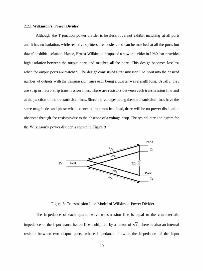
2.2.1 Wilkinson’s Power Divider
Although the T junction power divider is lossless, it cannot exhibit matching at all ports
and it has no isolation, while resistive splitters are lossless and can be matched at all the ports but
doesn’t exhibit isolation. Hence, Ernest Wilkinson proposed a power divider in 1960 that provides
high isolation between the output ports and matches all the ports. This design becomes lossless
when the output ports are matched. The design consists of a transmission line, split into the desired
number of outputs with the transmission lines each being a quarter wavelength long. Usually, they
are strip or micro strip transmission lines. There are resistors between each transmission line and
at the junction of the transmission lines. Since the voltages along these transmission lines have the
same magnitude and phase when connected to a matched load, there will be no power dissipation
observed through the resistors due to the absence of a voltage drop. The typical circuit diagram for
the Wilkinson’s power divider is shown in Figure 9
Figure 8: Transmission Line Model of Wilkinson Power Divider.
The impedance of each quarter wave transmission line is equal to the characteristic
impedance of the input transmission line multiplied by a factor of √2. There is also an internal
resistor between two output ports, whose impedance is twice the impedance of the input

20
transmission line. These impedances help isolate the output ports of the divider while matching
the input [7]. The S-matrix for a typical divider with the above-mentioned properties can be given
as:
[𝑆]= −𝑗
√2[0 1 11 0 01 0 0
] (2.21)
This matrix represents power entering through port 1 being divided between port 2 and
port 3. Since the ports are matched, 𝑆11, 𝑆22 and 𝑆33are zero. We know that for any lossless device,
the sum of the squares of the first column elements in the S-matrix are unitary [13].
It is observed that when the signal is applied at port 2, half of the power of the incident
signal is observed at port 1 while the other half is dissipated through the resistor connected at the
junction, but reciprocity is attained. Hence, 𝑆21=𝑆12. Due to the isolation between the output ports,
we cannot observe any power at port 3 when signal is applied at port 2 for an ideal Wilkinson
divider.
If two signals with the same amplitude and phase are applied at both output ports, port 2
and port 3 of an equally split Wilkinson divider, the sum of incident signals is observed at port 1,
the input port. This is because, the signals are in phase and no power is dissipated through the
resistor. These signals interfere constructively at the junction so, the divider acts as a power
combiner.
Wilkinson power dividers can be cascaded, or a single divider can have many output ports.
When a divider is cascaded to obtain multiple output ports, isolation between the output ports it
more likely to be maintained. The characteristic impedance of the quarter wave transmission line
(𝑍𝜆/4) for a given number of output ports n, an input impedance 𝑅𝑠, and load impedance 𝑅𝐿 is
given as:
𝑍𝜆/4= √𝑛 𝑅𝑠𝑅𝐿 (2.22)
21
Furthermore, as the number of output ports increases, the isolation between these ports decreases
[17]. Table 2 gives the information about the effect of isolation and theoretical insertion loss with
number of output ports.
Table 2: Isolation and Insertion Losses for Number of Output Ports [17] [15].
Number of output ports Theoretical Insertion Loss (dB) Isolation (dB)
2 3 ∞
4 6 21.6
6 7.8 17.6
8 9 16.1
3 4.8 ∞
5 7 19.5
Due to the lossless nature of the power divider under matched conditions, and the ease of
designing and constructing the circuit using micro strip lines, the Wilkinson power divider is an
ideal design to employ power division and is further studied.
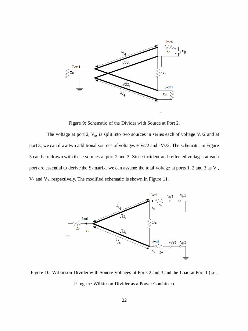
2.3 Even and Odd Mode Analysis on Wilkinson Divider
The performance of the divider can be analyzed with the effects of even and odd mode
impedances of the coupled lines on the S parameters, since impedance is a vector quantity which
is the ratio of electromagnetic voltage to current. To obtain the S-matrix, incident and reflected
voltages, we employed superposition and circuit symmetry. Initially, a Wilkinson divider with
source voltage of Vg at port 2 is considered and the rest of the ports are matched with impedance
of Z. The circuit schematic is shown in Figure 10. To simplify this schematic, the ground plane is
removed, which includes the bottom conductor of the transmission lines [15] [16].
22
Figure 9: Schematic of the Divider with Source at Port 2.
The voltage at port 2, Vg, is split into two sources in series each of voltage Vs/2 and at
port 3, we can draw two additional sources of voltages + Vs/2 and -Vs/2. The schematic in Figure
5 can be redrawn with these sources at port 2 and 3. Since incident and reflected voltages at each
port are essential to derive the S-matrix, we can assume the total voltage at ports 1, 2 and 3 as V1,
V2 and V3, respectively. The modified schematic is shown in Figure 11.
Figure 10: Wilkinson Divider with Source Voltages at Ports 2 and 3 and the Load at Port 1 (i.e.,
Using the Wilkinson Divider as a Power Combiner).
23
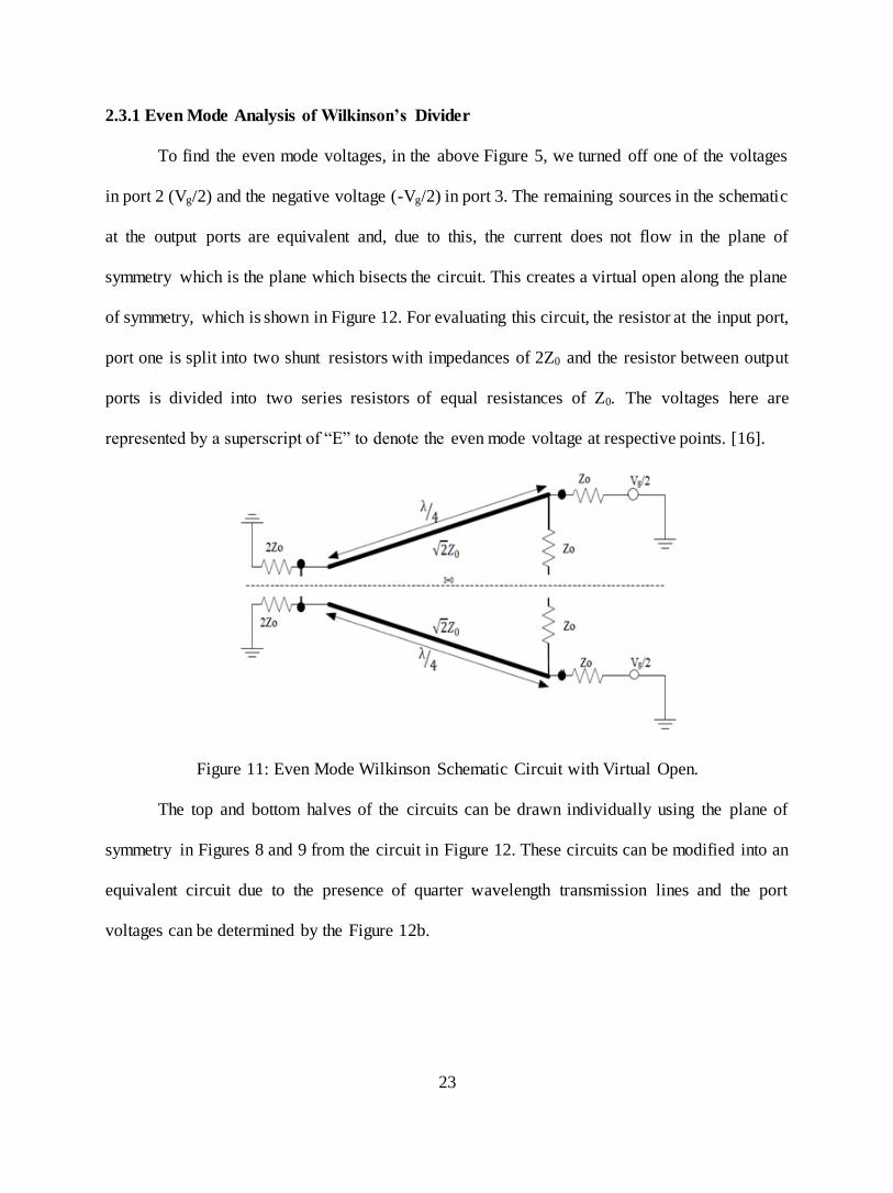
2.3.1 Even Mode Analysis of Wilkinson’s Divider
To find the even mode voltages, in the above Figure 5, we turned off one of the voltages
in port 2 (Vg/2) and the negative voltage (-Vg/2) in port 3. The remaining sources in the schematic
at the output ports are equivalent and, due to this, the current does not flow in the plane of
symmetry which is the plane which bisects the circuit. This creates a virtual open along the plane
of symmetry, which is shown in Figure 12. For evaluating this circuit, the resistor at the input port,
port one is split into two shunt resistors with impedances of 2Z0 and the resistor between output
ports is divided into two series resistors of equal resistances of Z0. The voltages here are
represented by a superscript of “E” to denote the even mode voltage at respective points. [16].
Figure 11: Even Mode Wilkinson Schematic Circuit with Virtual Open.
The top and bottom halves of the circuits can be drawn individually using the plane of
symmetry in Figures 8 and 9 from the circuit in Figure 12. These circuits can be modified into an
equivalent circuit due to the presence of quarter wavelength transmission lines and the port
voltages can be determined by the Figure 12b.

24
Figure 12a: Half Circuit of Even Mode
Wilkinson Divider.
Figure 12b: Simplified Even Mode Circuit.
The voltages at the end of each node was determined by voltage division and, since these
circuits are identical for even mode, the voltages are Vg/4 for 𝑉2𝐸 and 𝑉3
𝐸. The value of 𝑉1𝐸 cannot
be determined directly and hence, we apply voltage division across the 2Z0 resistor and by
multiplying the resistance and current flow across the voltage drop as -jVg/2√2.[15].
2.3.2 Odd Mode Analysis of Wilkinson’s Divider
The odd mode symmetry is observed when the even sources are turned off in the
equivalent circuit of the Wilkinson’s divider showed in Figure 10. Along the line of symmetry, i.e.
where the circuit is divided into symmetrical sub circuits, the voltages at port 2 and 3 cancel out
because they are 180 out of phase, which results in the formation of a virtual ground. Like the
even mode analysis, we can split the resistor at port 1 to two shunt resistors, each of value 2*Z0.
The voltage at node 1 is split into two nodes but since there is only one node, we can represent this
with a short circuit between the nodes. The resistor between the output ports 2 and 3, is divided
into resistors of equal resistance Z0 in series. Since we are analyzing the odd mode divider, the
voltages V1, V2 and V3 are now represented with a superscript “O” [15]. The equivalent odd mode
Wilkinson’s divider is shown below Figure 13.

25
Figure 13: Equivalent Circuit of the Odd Mode Wilkinson’s Divider.
The transmission line in the above figure is terminated with a short circuit, thus the input
impedance can be determined as.
Zin =Z0 𝑍𝐿+𝑗𝑍𝑜 𝑡𝑎𝑛𝛽𝑙
𝑍𝑜+𝑗𝑍𝐿𝑡𝑎𝑛𝛽𝑙 (2.23)
here, Z0 is the characteristic impedance of quarter wave transmission line, ZL is the load impedance
of the short-circuited line and β is the electrical length, equal to 2π/λ. Hence, the input impedance
can be written as
Zin = 𝑍0
2
𝑍𝐿 (2.24)
In the odd mode analysis, the voltages can be easily determined with voltage division and
the voltages at the second and third ports are 𝑉2𝑜 and 𝑉3
𝑜 are Vg/4 and -Vg/4, respectively, and the
voltage at port 1 is 𝑉10 which is 0. The odd mode and even mode voltages at each port are written
in the following Table 3.
Table 3: Port Voltages of Odd Mode and Even Mode Analysis of Wilkinson’s Divider
Port voltages Odd mode Analysis Even mode Analysis
𝑉10 𝑉1
𝐸 0 -jVg/2√2
𝑉20 𝑉2
𝐸 Vg/4 Vg/4
𝑉30 𝑉3
𝐸 -vg/4 Vg/4

26
By applying the principle of superposition, the even mode and odd mode port voltages are
summed up to get the total voltages as shown in Table 4. After determining these, we can derive
the scattering matrix by observing the incident and reflected voltages at all ports. But since ports
1 and 3 are matched, the supply is given to port 2 as shown in Figure 10.
Table 4: Voltages at Each Port of Power Divider
Ports Total voltages Incident voltage Reflected voltage
1 -jVg/2√2 0 -jVg/2√2
2 Vg/2 Vg/2 0
3 0 0 0
If the source is given at port 3 instead of port 2, we can derive the values in the third
column of the s-matrix. This is due to the bilateral symmetry of the Wilkinson’s divider. Hence,
S12 is equals S13, S23 equals S32 and S22 equals S33. Since Wilkinson’s dividers are reciprocal, when
the source is at port 1, the values of S21 and S31 are equal to S12 and S13. We know that the source
matched at port is 0 i.e. S11 is equal to zero [16].
S12= 𝑉1
−
𝑉2+ =
−𝑗𝑉𝑔
√2 (2.25)
S22= 𝑉2
−
𝑉2+= 0 (2.26)
S32= 𝑉3
−
𝑉2+ = 0 (2.27)
Hence the scattering matrix of the Wilkinson’s divider is derived as
[𝑆]= −𝑗
√2[0 1 11 0 01 0 0
] (2.28)

27
When the source is driving Port 2 of the power divider, we can see that only half the power
is transmitted to the load (Port 1) since half the power is dissipated through the resistor. The same
result is observed when driving Port 3 as shown by equations 2.29 and 2.30.
[𝑆]= −𝑗
√2[0 1 01 0 00 0 0
] (2.29)
[𝑆]= −𝑗
√2[0 0 10 0 01 0 0
] (2.30)
It can be observed that the power divider is lossy when the sources are applied at Port 2
and Port 3 separately. However, when the power source is applied at both Ports 2 and 3
simultaneously, we observe that the power divider acts as a power combiner due to the reciprocity
property of the device. This is possible because the incident voltage waves are in-phase and thus
add constructively in the device.
[𝑆]= −𝑗
√2[0 1 11 0 01 0 0
] (2.31)
The scattering matrix of Wilkinson’s power divider and combiner were derived, and the
performance characteristics of the device were also studied by incorporating the concepts of
superposition and conducting even mode and odd mode analysis. Since scattering matrix has
incident and reflected voltages, by supplying sources to one of the ports and by matching another
port, we derived the incident and reflected voltages at each mode and constructed a scattering
matrix, which shows the performance of the power divider at the given frequency and the
characteristic impedance of the system since, the elements in matrix vary as function of frequency.

28
CHAPTER 3
RF TRANSISTORS TESTING
An amplifier is an electronic device used to increase the magnitude of the input signals.
The amplification is measured in terms of gain. Voltage, current or power can be amplified, the
gain of an amplifier is the ratio output signal’s (voltage, current or power) compared to the original
input signal. These are active devices which depend on the input power of the signals and are used
widely in wireless communications and in broadcasting to boost the received signals. The signal
received by the receiver plays a major role in determining the strength of the communication link.
However, the signal transmitted by the transmitter has low power and high noise, to achieve better
communication power of the signal should be amplified, and noise should be reduced after
receiving the signal, which is accomplished by using amplifiers. Depending upon their functions,
amplifiers are divided into four types and are discussed further in this chapter.
3.1 RF Transistor Validation
Global ETS is an electronic testing company, which authenticates electronic devices and
is located in Odessa, Florida. They are an ISO 17025 certified and Defense Logistics Agency
(DLA) approved laboratory, specializing in authentication process and testing of electronic devices
with greater accuracy than other vendors. The company performs Visual Inspection, Decapsulation
and X Ray inspection of electronic components in an attempt to ensure that these components are
authentic and not counterfeit parts. As a RF/Microwave Intern in Dr. Saddow’s group assigned to
Global ETS, I got to work on different devices from leading manufacturing companies. I designed
test circuit boards using Agilent™ Advanced Design Software and performed RF functionality

29
tests using a M9372A Pxle Vector Network Analyzer (VNA). The most commonly tested devices
were RF transistors, typically used as power and buffer amplifiers in applications like cellular
repeater circuits, pre-driver amplifiers in transceiver systems and in Defense systems as signal
jammers. In this research a transistor was provided by Global ETS and an amplifier circuit board
was designed and fabricated at USF using LPKF ProtoMat S62 and LPKF ProtoMat S63 milling
machine. The fabricated board was further tested to verify if the amplifier met the specifications
provided by the manufacturer.
3.1.1 RF Amplifiers
Amplifiers are the active electronic devices that increase the voltage, current or power of
any input signals. Usually, amplifiers are used in wireless communications, audio equipment,
broadcasting and in many wireless applications [3]. Microwave amplifiers are used over a broad
range of frequencies [18]. Types of amplifiers usually used in RF applications are:
• Low Noise Amplifiers
• Power Amplifiers
• Linear Signal Amplifiers
• Driver Amplifiers
Low noise Amplifiers are the devices which are used to amplify the low power signals
usually received from an antenna without amplifying the noise present in the signals by minimizing
additional noise. The role of an LNA is to amplify signals and maintain the signal to noise ratio
(SNR) to prevent the loss of information and are used at the initial stage in receiver circuits shown
in Figure 14. Since low noise amplifiers are low power consuming devices, they provide voltage
gain instead of delivering power to the load [19].

30
Figure 14: Simple Block Diagram of Transceiver Circuit.
The simple block diagram of a transceiver circuit showing the LNA in the receive signal
path (top). The PA is in the transmit path (bottom). The duplexer ensures that the transmit power
is isolated from the receiver circuit during receive operation. One of the most commonly used
devices in many RF applications to boost the RF signal is a power amplifier (PA). As the name
suggests, a power amplifier is an electronic device used to amplify low power radio frequency
signals and is typically used in transmitter circuits to drive the transmit antenna. Usually the design
specifications include gain, output power, efficiency, P1dB point (Output power at 1dB
compression of gain), OIP3 (Output third Intercept Power) and heat dissipation. The PA often
includes input and output impedance matching circuits.
Modern power amplifiers operate in different modes to help achieve the desired design
goals. These modes are called classes and some of them are Class A, B, AB, C, D, E and F. Usually
for RF applications, Class D amplifiers are not chosen due to their tendency to deteriorate
efficiency. This usually happens due to the saturated charge storage and finite switching speed of
active devices. Many RF amplifiers are made of solid-state devices like bipolar junction transistors,
MOSFETs, and MESFETs [18].
Linear signal amplifiers are general amplifiers, referred sometimes as gain block
amplifiers, to provide signal gain within the system. These amplifiers do not determine the

31
dynamic range of a system since they are not located either at the input or at the output of the
circuit. Linear signal amplifiers are preferred for their convenience factors such as moderate cost,
size and power consumption, which is greater than a low noise amplifier and lesser than a power
amplifier and are internally matched. Applications of these amplifiers are significant in industries
such as wireless infrastructure, defense, and in transceiver systems to provide internal gain.
Driver amplifiers are used specifically to amplify continuous wave signals at a single
frequency and are frequently used in the creation of a local oscillator signal for mixers or in
synthesizers. Employing these amplifiers generates maximum performance of the system in
electronic warfare, and instrumentation and measurement applications. They are often integrated
into CMOS circuits in the transceiver chip in many consumer applications. Efficiency is of greatest
concern in driver amplifiers, due to their usage in super heterodyne systems to generate local
oscillator signals with power of typically 6 to 10 dB more than the original signal. Due to this,
these amplifiers have higher power levels than low noise amplifiers [19].
The applications of each of these amplifiers can be summarized in the following block
diagram of the super heterodyne system, which is often used in a radio communication links, radar,
imaging systems, satellite and in repeater circuits:
Figure 15: Transmission System Employing Different Amplifier Types as Shown (LNA, PA,
Driver, etc.).

32
Figure 16: Receiver System Employing Different Amplifier Types as Shown (LNA, PA, Driver,
etc.).
The following table summarizes amplifier types and their advantages/Figure of Merit, along with
their common applications.
Table 5: Types of Amplifiers and Their Properties
Type of Amplifier Application Figure of Merit
Low Noise
Amplifier
Amplifying the received signals by
antenna
Voltage Gain, Noise Figure,
Signal to Noise Ratio (SNR)
Power Amplifier
Amplifying the signals for
transmission
Efficiency, linearity
Linear Signal
Amplifier
Removing system losses Gain, Noise Figure and linearity
Driver Amplifier Generating local Oscillator signals
Phase Noise and Harmonics
reduction
3.2 Amplifiers Boards Designed at Global ETS, LLC
3.2.1 Qorvo SGA 3263Z Amplifier
The internship experience at Global ETS, LLC can be summarized as working on three
different amplifier boards. One of the boards was designed and fabricated at the company but was

33
tested using a Vector Network Analyzer (VNA), Spectrum Analyzer (SA) and a Noise Figure (NF)
meter at the Center for Wireless and Microwave Information Systems (WAMI) at USF. The
transistor, Qorvo SGA 3263Z, was manufactured by Qorvo and is a high performance SiGe
Monolithic Microwave Integrated Circuit (MMIC) Amplifier. It acts as a broadband amplifier with
a bias supply voltage of 5V. It can be used as a PA Driver amplifier, IF (intermediate frequency)
amplifier and has applications in cellular repeater circuits, GSM boost circuits, Wireless
Infrastructure, satellite communications, Gain Flatness Compensation circuit and acts a Gain
Block Active Bias Circuit in point to point radio communications. The pin-out diagram of this
transistor is shown in Figure 17.
Figure 17: Transistor Pin Diagram of the Qorvo SGA3263Z RF Transistor.
This is an HBT in the Darlington configuration. The SGA 3263Z is a Darlington
configuration SiGe (Silicon Germanium) Heterojunction Bipolar Transistor. A Darlington
configuration is combination of transistors, which acts as a single transistor with higher current
gain (sometimes this is referred to as a ‘super Beta’ transistor [21]. The advantages of using a
Darlington pair is with a small base current, a large load can be driven, and heterojunction
transistors are popular because of lower leakage currents at the junctions and higher breakdown
voltages [3]. The pins 3 and 6 are for RF signal input and RF signal output, and the rest of the pins
1,2,4, and 5 are common ground pins which are grounded. The input signal entered through pin 3
is amplified and collected at the output pin 6. The schematic diagram of this transistor and the
fabricated board are shown in Figures 18 and 19. The fabricated amplifier board was then tested,
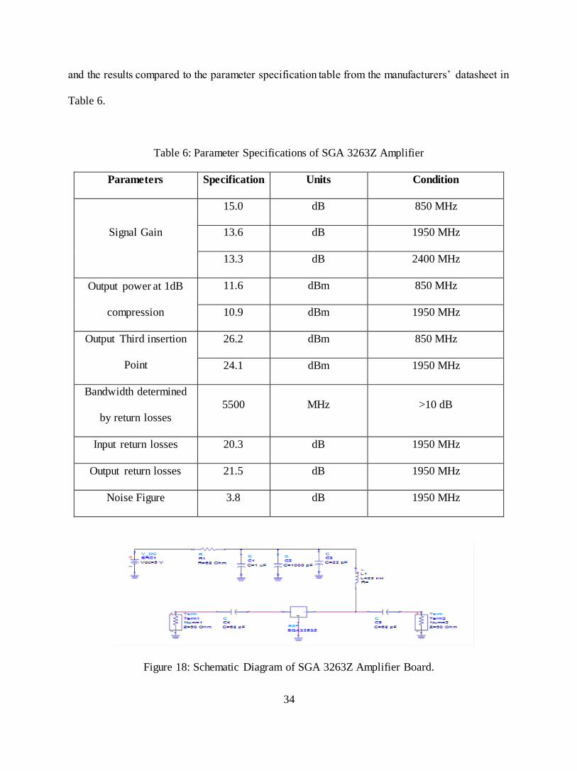
34
and the results compared to the parameter specification table from the manufacturers’ datasheet in
Table 6.
Table 6: Parameter Specifications of SGA 3263Z Amplifier
Parameters Specification Units Condition
Signal Gain
15.0 dB 850 MHz
13.6 dB 1950 MHz
13.3 dB 2400 MHz
Output power at 1dB
compression
11.6 dBm 850 MHz
10.9 dBm 1950 MHz
Output Third insertion
Point
26.2 dBm 850 MHz
24.1 dBm 1950 MHz
Bandwidth determined
by return losses
5500 MHz >10 dB
Input return losses 20.3 dB 1950 MHz
Output return losses 21.5 dB 1950 MHz
Noise Figure 3.8 dB 1950 MHz
Figure 18: Schematic Diagram of SGA 3263Z Amplifier Board.

35
The circuit has two DC blocking capacitors at the input and output terminals and a DC feed
inductor, known as an RF choke, which blocks RF signals and allows DC signals to pass through
it. The bias circuit consists of a 68Ω bias resistor, which was in the datasheet at this voltage and
operational frequency. From this schematic design, a layout can be generated, and a PCB can be
fabricated to test the transistors as shown in the Figure 19.
Figure 19: Fabricated PCB of SGA 3263Z from Global ETS, LLC.
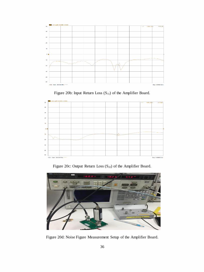
The VNA was first calibrated over the frequency range of 300 MHz to 3 GHz using the
WAMI calibration kit, called SOLT calibration. Next the Device Under Test, the amplifier board,
was placed between the ports of the VNA and the S parameters observed are shown in Figure 20.
Figure 20a: Gain (S21) dB of the Amplifier Board of Figure 19.
36
Figure 20b: Input Return Loss (S11) of the Amplifier Board.
Figure 20c: Output Return Loss (S22) of the Amplifier Board.
Figure 20d: Noise Figure Measurement Setup of the Amplifier Board.
37
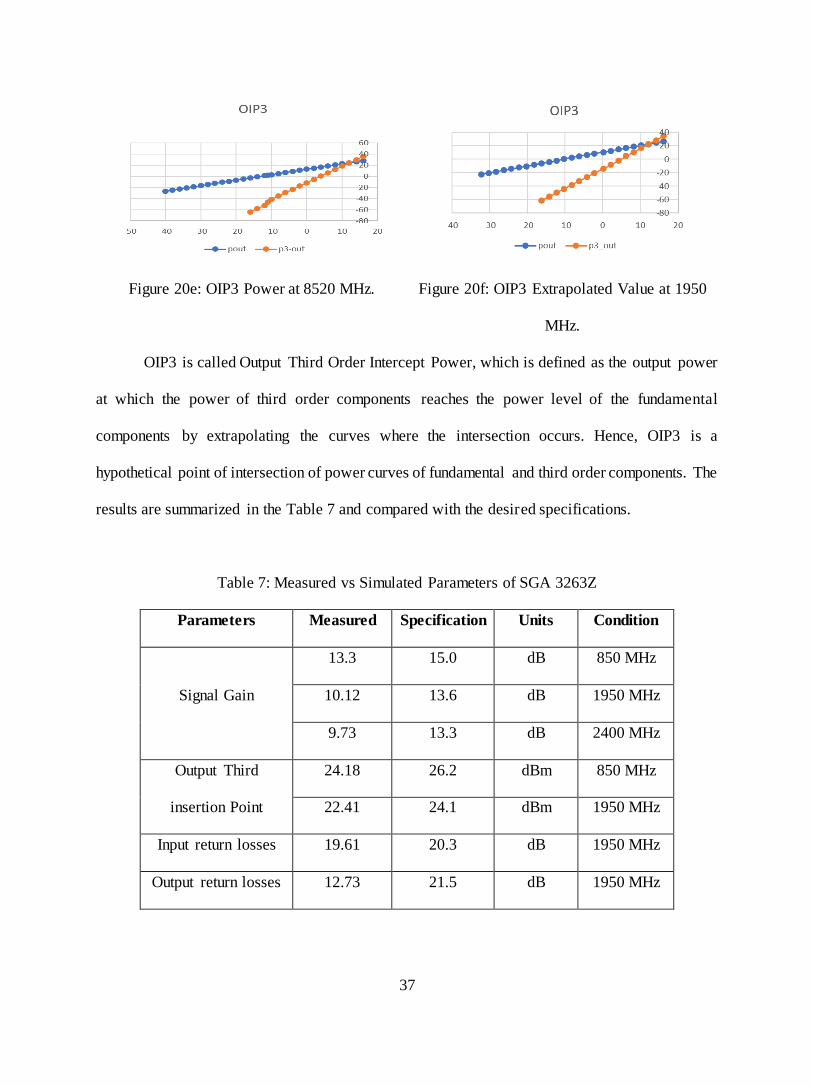
Figure 20e: OIP3 Power at 8520 MHz. Figure 20f: OIP3 Extrapolated Value at 1950
MHz.
OIP3 is called Output Third Order Intercept Power, which is defined as the output power
at which the power of third order components reaches the power level of the fundamental
components by extrapolating the curves where the intersection occurs. Hence, OIP3 is a
hypothetical point of intersection of power curves of fundamental and third order components. The
results are summarized in the Table 7 and compared with the desired specifications.
Table 7: Measured vs Simulated Parameters of SGA 3263Z
Parameters Measured Specification Units Condition
Signal Gain
13.3 15.0 dB 850 MHz
10.12 13.6 dB 1950 MHz
9.73 13.3 dB 2400 MHz
Output Third
insertion Point
24.18 26.2 dBm 850 MHz
22.41 24.1 dBm 1950 MHz
Input return losses 19.61 20.3 dB 1950 MHz
Output return losses 12.73 21.5 dB 1950 MHz

38
Table 7 continued
Parameters Measured Specification Units Condition
Noise Figure 4.3 4.1 dB 1950 MHz
We can observe that, at higher frequencies, there is a deviation in the measured results and
the desired specifications. This is most likely because of parasitics - since the transistor is internally
matched, we did not design any external matching circuits, and this could also impact the measured
results.
3.2.2 Qorvo SGA 5586Z Amplifier
The amplifier board was designed for Qorvo’s SGA5586Z, which is also a Darlington
configuration HBT amplifier. The pinout diagram for the transistor is shown in Figure 21. Since
the amplifier is internally matched, matching circuits were not included in the design.
Figure 21: Pin Diagram of SGA5586Z HBT Transistor Darlington Pair.
Pin 1 and 3 are the emitters, pin 4 is the base and pin 2 is the collector of the transistors.
The mode of operation is common emitter since the emitter is common to both input and output
terminals of the amplifier circuit. The input signal is applied between the base and emitter (ground)
and the output signal is measured between the collector and emitter (ground) of the transistor. This
configuration is usually preferred because of the high transconductance, or voltage, provided for
the given load and is used in many day to day applications of power amplifiers. This circuit consists
of a DC block capacitor, DC feed inductor (RF choke) and a bias resistor in a bias circuit.
39
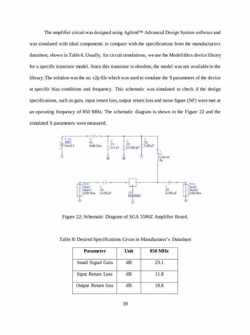
The amplifier circuit was designed using Agilent™ Advanced Design System software and
was simulated with ideal components to compare with the specifications from the manufacturers
datasheet, shown in Table 6. Usually, for circuit simulations, we use the Modelithics device library
for a specific transistor model. Since this transistor is obsolete, the model was not available in the
library. The solution was the an. s2p file which was used to simulate the S parameters of the device
at specific bias conditions and frequency. This schematic was simulated to check if the design
specifications, such as gain, input return loss, output return loss and noise figure (NF) were met at
an operating frequency of 850 MHz. The schematic diagram is shown in the Figure 22 and the
simulated S parameters were measured.
Figure 22: Schematic Diagram of SGA 5586Z Amplifier Board.
Table 8: Desired Specifications Given in Manufacturer’s Datasheet
Parameter Unit 850 MHz
Small Signal Gain dB 23.1
Input Return Loss dB 11.8
Output Return loss dB 18.8
40
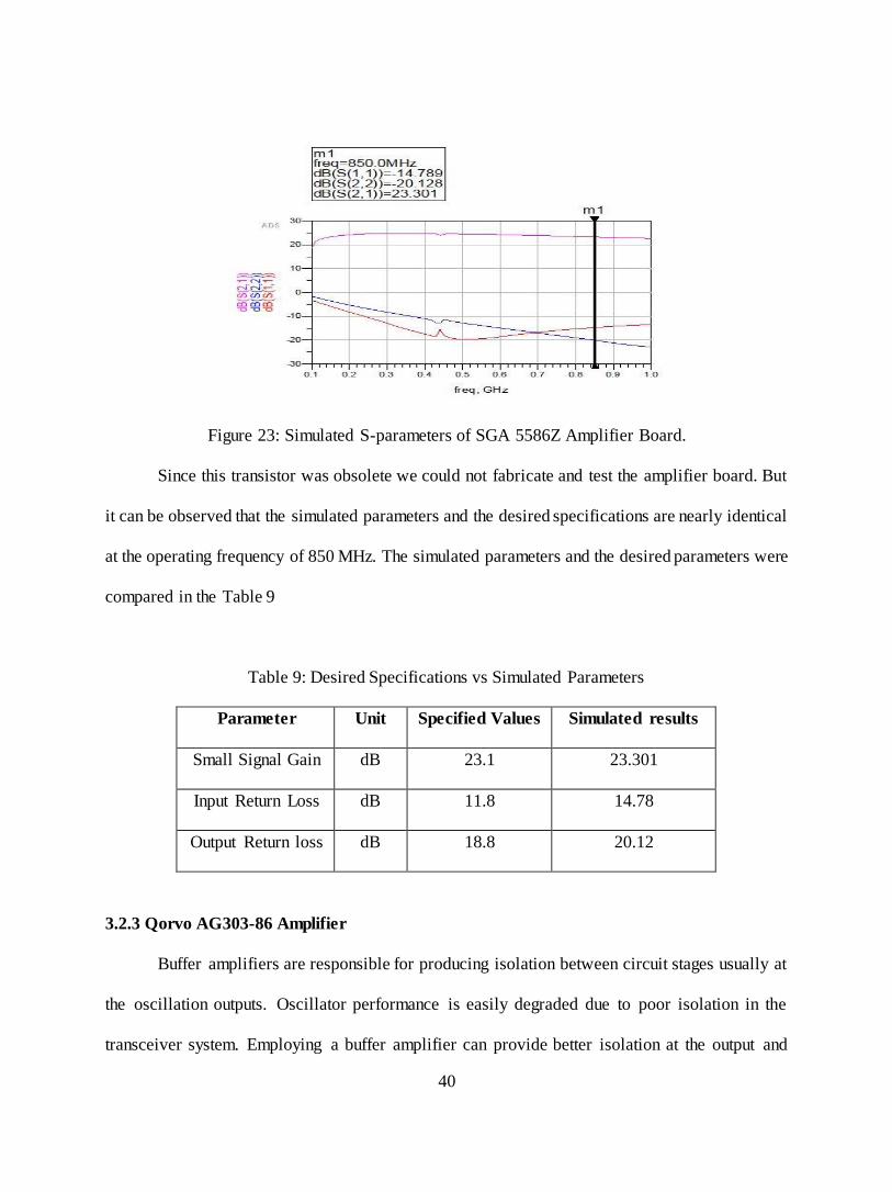
Figure 23: Simulated S-parameters of SGA 5586Z Amplifier Board.
Since this transistor was obsolete we could not fabricate and test the amplifier board. But
it can be observed that the simulated parameters and the desired specifications are nearly identical
at the operating frequency of 850 MHz. The simulated parameters and the desired parameters were
compared in the Table 9
Table 9: Desired Specifications vs Simulated Parameters
Parameter Unit Specified Values Simulated results
Small Signal Gain dB 23.1 23.301
Input Return Loss dB 11.8 14.78
Output Return loss dB 18.8 20.12
3.2.3 Qorvo AG303-86 Amplifier
Buffer amplifiers are responsible for producing isolation between circuit stages usually at
the oscillation outputs. Oscillator performance is easily degraded due to poor isolation in the
transceiver system. Employing a buffer amplifier can provide better isolation at the output and
41
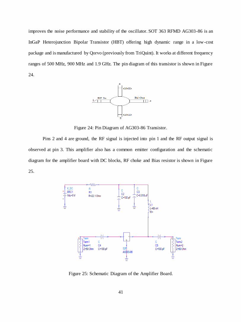
improves the noise performance and stability of the oscillator. SOT 363 RFMD AG303-86 is an
InGaP Heterojunction Bipolar Transistor (HBT) offering high dynamic range in a low-cost
package and is manufactured by Qorvo (previously from TriQuint). It works at different frequency
ranges of 500 MHz, 900 MHz and 1.9 GHz. The pin diagram of this transistor is shown in Figure
24.
Figure 24: Pin Diagram of AG303-86 Transistor.
Pins 2 and 4 are ground, the RF signal is injected into pin 1 and the RF output signal is
observed at pin 3. This amplifier also has a common emitter configuration and the schematic
diagram for the amplifier board with DC blocks, RF choke and Bias resistor is shown in Figure
25.
Figure 25: Schematic Diagram of the Amplifier Board.

42
The schematic diagram has transmission lines and the ideal lumped elements which were
replaced with Modelithics elements to consider parasitic effects at the operating frequency. The
emitter is grounded using a via and the footprint of the transistor can be drawn according to the
manufacturer’s datasheet, while the transmission lines were replaced by microstrip transmission
lines. The substrate used was FR4. External matching circuits were not designed since the
manufacturer’s datasheet mentioned that the transistor is matched internally. The quantity of the
amplifiers to be tested were more than 6000 so a rapid test method was required. We tested the
gain of the amplifier board and utilized a test socket to replace the device under test instead of
designing a board and soldering in the transistor package separately for each device. Figure 26
shows one of the test sockets for testing an amplifier board.
Figure 26: RF Test Socket on the PCB to Test Each of 6000 RFMD AG303-86 InGaP HBTs.

43
Figure 27: Layout of AG303-86G Amplifier Board.
We did not have the Modelithics model of the transistor, only the mechanical footprint
drawing information from the datasheet. The foot prints of the lumped elements are due to the
components from the Modelithics library, which consider the parasitic effects at the operating
frequency. The assembled board for testing is shown in Figure 28.
Figure 28: Assembled Board of the Amplifier Containing the TriQuint AG303-86.
The fabricated board was milled with an LPKF ProtoMat S63 using FR4 as the substrate
and the lumped elements were assembled. This board was later tested using a Vector Network
Analyzer after performing SOLT (short-Open-Load-Thru) calibration. This calibration is usually

44
performed to shift the reference plane from the ports of VNA to the Device Under Test (DUT)
ports. The gain was measured by observing S21 at the operating frequency, shown in Figure 29.
Figure 29: Measured Gain of the TriQuint AG303-86G InGaP HBT Amplifier Board from 300
MHz to 2 GHz.
It is observed that the measured gain was equal and meets the desired gain at the operating
frequency. The gain of the amplifier at 900 MHz, 500 MHz and 1.9 GHz was 19.45 dB, 20.20 dB
and 16.89 dB, respectively, which meets the desired conditions. The Table 10 shows the desired
and measured parameters at different frequencies.
Table 10: Gain (dB) vs Frequencies (MHz) AG303-86 Amplifier
Frequency Gain (dB)
500 MHz 20.20
900 MHz 19.45
1.9 GHz 16.89

45
CHAPTER 4
DESIGN AND FABRICATION
In the field of Microwave and RF devices, power dividers are typically passive devices
which couple power in the form of electromagnetic waves from one port allowing the signal to be
used in other ports or circuits. Wilkinson’s power divider helps in achieving isolation between the
load ports while maintaining matched conditions at all the ports. Since the power divider is a
passive device, it can also act as a power combiner due to the reciprocal properties of the device.
The design, construction and simulation results are discussed in this chapter.
4.1 Microstrip Transmission Lines and Dimensions
Microstrip lines are often used to build active and passive circuit boards since fabrication
techniques like milling and photolithography are easily adopted. Microstrip technology is compact
and economical when compared to waveguide technology. It has a dielectric layer called the
substrate which separates the conductive signal layer from a metal ground plane. The microstrip
layout with conductor width W, substrate thickness H and substrate permittivity ℇr [13] is shown
in Figure 30. The disadvantages of using microstrip transmission lines are that they are unable to
handle high frequency signals, have lower power handling capacity and more losses than hollow-
pipe metal waveguides. Microstrip lines exhibit interference between traces due to signal radiation
and cross talk since they are not enclosed like waveguides. FR4 and Alumina are the most
commonly used dielectrics [22] used at these frequencies.

46
Figure 30: Microstrip Transmission Line on a Substrate with Relative Permittivity ℇr.
Since the dielectric separates signal line and ground plane, the absence of the substrate
implies the presence of air, which leads to the TEM mode of propagation (transverse
electromagnetic mode). Due to the non-ideal dielectric between the conductor (microstrip line)
and the ground plane, a perfect TEM mode of propagation is not possible for microstrip lines [13].
When the wavelength is longer than the substrate thickness, the so-called quasi TEM mode of
propagation is observed, which is very close to the true TEM mode. While designing a microstrip
line, properties like width of conductor (W), propagation constant (β), phase velocity (vp)and
wavelength (λ) are considered and related by the formula (4.1)
Vp = λ
𝑇 (4.1)
= 𝑐
√ℇeff (4.2)
β= k√ℇeff (4.3)
where K is the propagation constant of free space (k=ω√µO ∗ ℇeff), C is the speed of light (3*108
m/s) and ℇeff is the effective dielectric constant of the substrate and air, which is a function of
relative permittivity of the substrate, width of the conductor and thickness of the substrate. The
relation between the wavelength (λ) of the microstrip line and the phase velocity is given by (4.4)
λ= 𝑐
𝑓∗√ℇeff (4.4)
where f is the operating frequency of the device in Hertz (Hz).
47
The characteristic impedance of a microstrip device also depend on the width of the
conductor and the dielectric thickness. Since Wilkinson’s power divider employs quarter
wavelength transmission lines, lengths and widths of these lines depends on the chosen substrate
and conductor thickness and are calculated using the Linecalc™ tool from Advanced Design
System (ADS™) software.
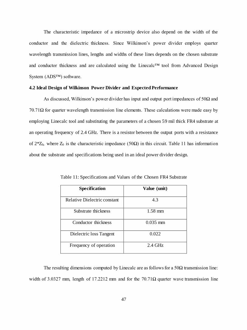
4.2 Ideal Design of Wilkinson Power Divider and Expected Performance
As discussed, Wilkinson’s power divider has input and output port impedances of 50Ω and
70.71Ω for quarter wavelength transmission line elements. These calculations were made easy by
employing Linecalc tool and substituting the parameters of a chosen 59 mil thick FR4 substrate at
an operating frequency of 2.4 GHz. There is a resistor between the output ports with a resistance
of 2*Z0, where Z0 is the characteristic impedance (50Ω) in this circuit. Table 11 has information
about the substrate and specifications being used in an ideal power divider design.
Table 11: Specifications and Values of the Chosen FR4 Substrate
Specification Value (unit)
Relative Dielectric constant 4.3
Substrate thickness 1.58 mm
Conductor thickness 0.035 mm
Dielectric loss Tangent 0.022
Frequency of operation 2.4 GHz
The resulting dimensions computed by Linecalc are as follows for a 50Ω transmission line:
width of 3.0327 mm, length of 17.2212 mm and for the 70.71Ω quarter wave transmission line
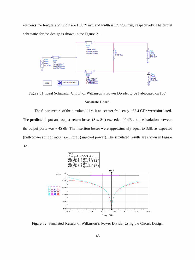
48
elements the lengths and width are 1.5839 mm and width is 17.7236 mm, respectively. The circuit
schematic for the design is shown in the Figure 31.
Figure 31: Ideal Schematic Circuit of Wilkinson’s Power Divider to be Fabricated on FR4
Substrate Board.
The S-parameters of the simulated circuit at a center frequency of 2.4 GHz were simulated.
The predicted input and output return losses (S11, S22) exceeded 40 dB and the isolation between
the output ports was ~ 45 dB. The insertion losses were approximately equal to 3dB, as expected
(half-power split of input (i.e., Port 1) injected power). The simulated results are shown in Figure
32.
Figure 32: Simulated Results of Wilkinson’s Power Divider Using the Circuit Design.

49
The device parameters observed were bandwidth, input return loss (S11), output return loss
(S22 and S33), isolation between output ports, power division or amplitude balance and phase
balance. Typically, manufactured power dividers available in the market were able to achieve 65:1
of bandwidth [16] with multiple quarter wavelength transmission line sections and a VSWR of
1.3:1 for input return losses greater than 15 dB and the VSWR of 13.48 dB [15]. Isolation is also
an important factor and values greater than 15 dB provide good isolation between the output ports
across the specified bandwidth. Depending upon the bandwidth of the device, the amplitude
balance is usually ±0.45 dB (difference in insertion losses). These values were observed for the
power dividers manufactured by the companies in the market. The results expected are
summarized in the Table 12.
Table 12: Commercial Wilkinson’s Power Divider Specifications [15]
Parameter Expected results
Isolation between output ports > 15dB
Output Port Amplitude Balance ±0.2 dB
Return Losses >15 dB
4.3 Design and Simulated Results of Wilkinson’s Power Divider
Since Wilkinson’s divider has many design topologies, different microstrip junctions were
designed and constructed with an operating at a frequency of 2.4 GHz. ADS™ software was used
for the designs. Circuit CAM 4.0™ and LPKF Circuit Board plotter™ software were used to
fabricate the power dividers. The results were observed using a Keysight PXle Vector Network
analyzer™.

50
4.3.1 Design and Construction of Curved Wilkinson Divider with Step Junction
As the name indicates, the design has a step junction between the quarter wavelength
transmission lines and 50Ω terminations at the output ports. The schematic is shown in the Figure
33.
Figure 33: Schematic Diagram of Curved Power Divider with Step Junction.
The step junction connects the conductor of width W1 (mm) at pin 1 to the conductor of
width W2 (mm) at pin 2. Usually a step junction is employed when two transmission lines of
different widths are connected in a circuit. The layout of this divider can be generated from the
schematic using Generate/update Layout tool in ADS™. The above schematic is simulated and
the parameters such as input and output return losses, isolation between the ports, insertion losses
observed are shown in Figure 34. To include the parasitic effects, a Modelithics (Tampa, FL)
resistor was used in the design between the output ports to provide isolation.

51
Figure 34a: Simulated Input Return Loss (S11) and Output Return Loss (S22, S33) in dB of
Design 1.
Figure 34b: Simulated Isolation between the Output Ports 2 and 3(S32, S23) in dB vs F (GHz) of
Design 1.
Figure 34c: Simulated Insertion Losses (S21, S31) in dB vs F (GHz) of Design 1.

52
It was observed that the input return losses and output return losses were greater than 40
dB, indicating more than 99.9% of the power was transferred. The device operates with better
amplitude balance within the frequency range of 1.63 - 3.21 GHz, with a center frequency of 2.28
GHz and providing the bandwidth of 70%. Bandwidth can be calculated by observing the lower
and higher frequencies of operation using the formula 4.5
BW= FH−FL
𝐹𝑐 *100% (4.5)
Fc= √FL ∗ FH (4.6)
where FL is the lowest frequency (FL = 1.632GHz), FH is the highest frequency (FH = 3.213GHz)
and the center frequency (Fc) was 2.28 GHz. The values of insertion losses were the same and
hence the power was divided equally. The isolation between the output is greater than 40 dB,
indicating that the output ports are isolated while the input port is matched to a 50Ω load.
4.3.2 Wilkinson Divider with Continuous Taper
This design is similar to the above design of the divider but has a continuous taper instead
of a microstrip step junction. The taper connects the transmission lines of different widths and
induces additional length to describe the widths of the transmission lines. The difference between
a microstrip step and tapered junctions are primarily observed in the design layout. The schematic
design of the divider circuit with tapered junction is shown in Figure 35. The length of the quarter
wave transmission line for this design was 17.0236 mm due to the tapered length of 0.7 mm.

53
Figure 35: Schematic Diagram of a Power Divider Circuit with Tapered Junction Between the
50Ω and 70.71 Ω Transmission Lines.
The above circuit is simulated over the range of 0.2- 4.0 GHz and the observed simulated
results are shown in the Figure 36.
Figure 36a: Simulated Input and Output Return Losses (S11, S22 and S33) in dB of Design 2.
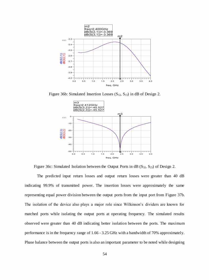
54
Figure 36b: Simulated Insertion Losses (S12, S13) in dB of Design 2.
Figure 36c: Simulated Isolation between the Output Ports in dB (S32, S23) of Design 2.
The predicted input return losses and output return losses were greater than 40 dB
indicating 99.9% of transmitted power. The insertion losses were approximately the same
representing equal power division between the output ports from the input port from Figure 37b.
The isolation of the device also plays a major role since Wilkinson’s dividers are known for
matched ports while isolating the output ports at operating frequency. The simulated results
observed were greater than 40 dB indicating better isolation between the ports. The maximum
performance is in the frequency range of 1.66 - 3.25 GHz with a bandwidth of 70% approximately.
Phase balance between the output ports is also an important parameter to be noted while designing
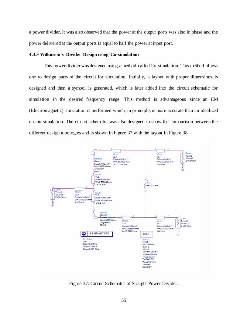
55
a power divider. It was also observed that the power at the output ports was also in phase and the
power delivered at the output ports is equal to half the power at input port.
4.3.3 Wilkinson’s Divider Design using Co-simulation
This power divider was designed using a method called Co-simulation. This method allows
one to design parts of the circuit for simulation. Initially, a layout with proper dimensions is
designed and then a symbol is generated, which is later added into the circuit schematic for
simulation in the desired frequency range. This method is advantageous since an EM
(Electromagnetic) simulation is performed which, in principle, is more accurate than an idealized
circuit simulation. The circuit schematic was also designed to show the comparison between the
different design topologies and is shown in Figure 37 with the layout in Figure 38.
Figure 37: Circuit Schematic of Straight Power Divider.

56
Figure 38: Layout of Straight Power Divider Using Co-simulation Method.
EM simulation was performed by assigning a substrate (FR4) (Fig. 39), with dielectric
constant, conductor and substrate thicknesses from Table 12. An EM simulation was performed,
and a symbol generated to measure the isolation after adding the output resistor. Terminations and
a KOA 100Ω resistor were added to the symbol, as shown in Figure 40, to perform the circuit
simulations.
Figure 39: Substrate Dimensions for Performing EM Simulation on Straight Power Divider.
Figure 40: Circuit Layout Created Using Co-sim Method Using the Straight Power Divider
Symbol.

57
The following S parameters were predicted after performing circuit simulations in the
frequency range of 300 MHz to 4 GHz.
Figure 41a: Insertion Losses in dB vs. F (GHz) of Design 3.
Figure 41b: Simulated Design 3 Input and
Output Return Losses.
Figure 41c: Simulated Design 3 Isolation.
From the above simulated data, it was observed that the input return losses were 40 dB
indicating that maximum power should be transferred, and output return losses were above 25 dB
indicating less than 0.1% of power was reflected. The insertion losses were equal indicating equal
power division. The isolation between the output ports was maximum at a frequency of 2.435 GHz.
These updated layouts were fabricated using the LPKF Protomat S62 milling machine.

58
4.3.4 Layouts of Power Divider Circuits
The layouts of power dividers designed using ADS is shown in Figures 42 a, b and c
Figure 42a, b: Step and Tapered Junction
Power Dividers.
Figure 42c: Straight Power Divider.
The quarter wavelength microstrip transmission lines have a common length of 17.73 mm
after optimizing the circuit to meet the specifications. The quarter wavelength transmission lines
were separated by 1 cm, which affects the performance of the divider due to coupling between the
transmission lines. Isolation is primarily affected by coupling across the gap between the
transmission lines.
4.4 Construction and Results
The divider boards were fabricated using LPKF S62 Protomat milling machine. Initially
the .dxf/dwg file was generated by the ADS™ software and then imported into the CircuitCAM
software for the machine to assign the excess copper and copper conductor traces and then
exported the file to. LMD extension for the fabrication process. This file was later imported in the
Board Plotter software to guide the milling process manually step-by-step by adjusting the
placement of the design on the substrate board for fabrication. The fabricated boards are shown in
Figure 43a, b and c.
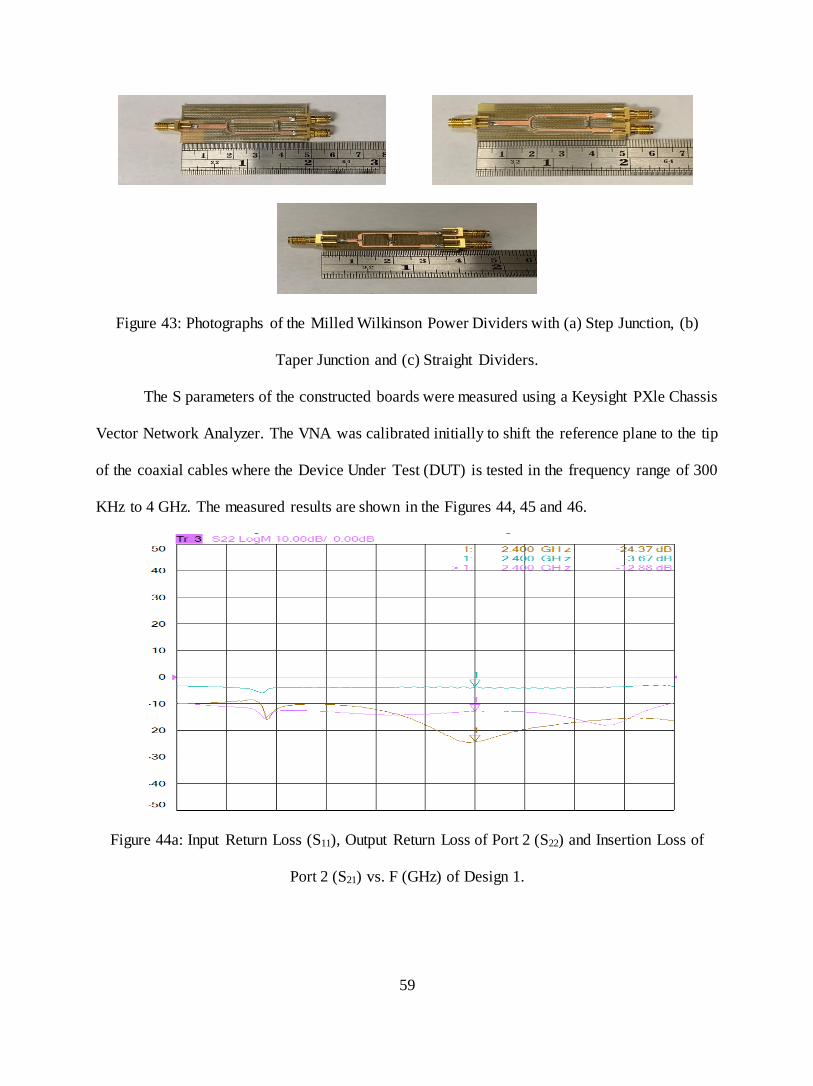
59
Figure 43: Photographs of the Milled Wilkinson Power Dividers with (a) Step Junction, (b)
Taper Junction and (c) Straight Dividers.
The S parameters of the constructed boards were measured using a Keysight PXle Chassis
Vector Network Analyzer. The VNA was calibrated initially to shift the reference plane to the tip
of the coaxial cables where the Device Under Test (DUT) is tested in the frequency range of 300
KHz to 4 GHz. The measured results are shown in the Figures 44, 45 and 46.
Figure 44a: Input Return Loss (S11), Output Return Loss of Port 2 (S22) and Insertion Loss of
Port 2 (S21) vs. F (GHz) of Design 1.
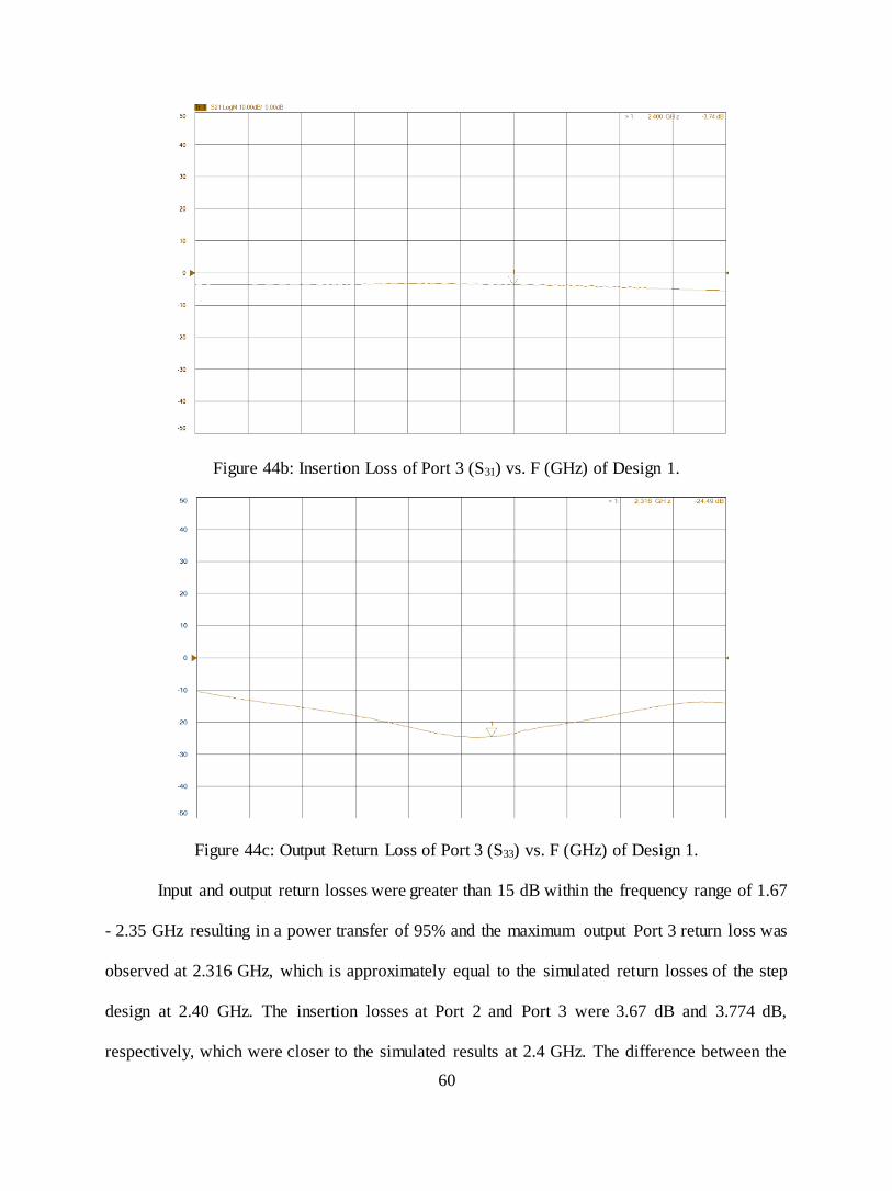
60
Figure 44b: Insertion Loss of Port 3 (S31) vs. F (GHz) of Design 1.
Figure 44c: Output Return Loss of Port 3 (S33) vs. F (GHz) of Design 1.
Input and output return losses were greater than 15 dB within the frequency range of 1.67
- 2.35 GHz resulting in a power transfer of 95% and the maximum output Port 3 return loss was
observed at 2.316 GHz, which is approximately equal to the simulated return losses of the step
design at 2.40 GHz. The insertion losses at Port 2 and Port 3 were 3.67 dB and 3.774 dB,
respectively, which were closer to the simulated results at 2.4 GHz. The difference between the

61
insertion losses of Ports 2 and 3 is called the Amplitude Balance and was observed as 0.07 dB,
indicating power division was almost equal between the output ports.
Figure 45a: Input Return Loss (S11), Output Return Loss of Port 2 (S22) and Insertion Loss of
Port 2 (S21) vs. F (GHz) of Design 2.
Figure 45b: Insertion Loss of Port 3 (S31) vs. F (GHz) of Design 2.
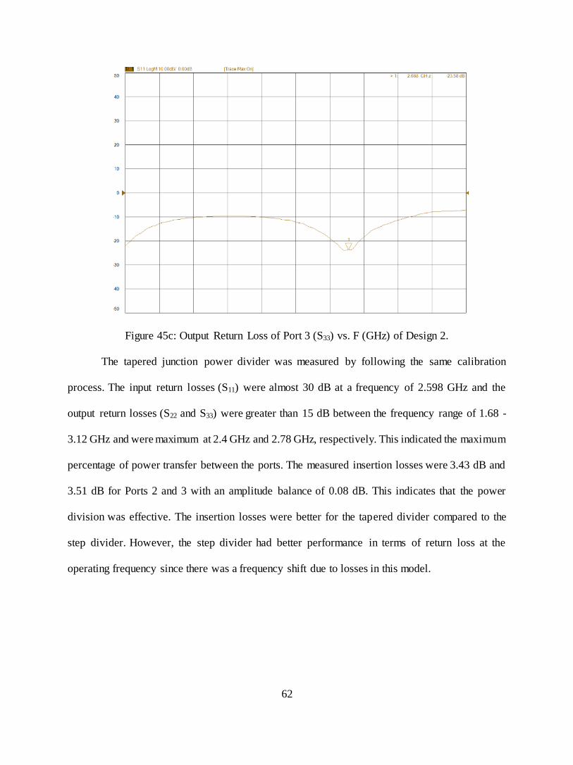
62
Figure 45c: Output Return Loss of Port 3 (S33) vs. F (GHz) of Design 2.
The tapered junction power divider was measured by following the same calibration
process. The input return losses (S11) were almost 30 dB at a frequency of 2.598 GHz and the
output return losses (S22 and S33) were greater than 15 dB between the frequency range of 1.68 -
3.12 GHz and were maximum at 2.4 GHz and 2.78 GHz, respectively. This indicated the maximum
percentage of power transfer between the ports. The measured insertion losses were 3.43 dB and
3.51 dB for Ports 2 and 3 with an amplitude balance of 0.08 dB. This indicates that the power
division was effective. The insertion losses were better for the tapered divider compared to the
step divider. However, the step divider had better performance in terms of return loss at the
operating frequency since there was a frequency shift due to losses in this model.

63
Figure 46a: Input Return Loss (S11), Output Return Loss (S22) and Insertion Loss (S21) vs. F
(GHz) of Design 3.
Figure 46b: Insertion Loss of Port 3(S31) vs. F (GHz) of Design 3.

64
Figure 46c: Output Return Loss of Port 3 (S33) vs F (GHz) of Design 3.
The input return losses were greater than 20dB indicating more than 98% of the power is
transferred to the output ports and the output return losses were greater than 15 dB indicating 95%
of power transfer at 2.07 GHz and 1.9 GHz for the measured straight divider. The insertion losses
of Ports 2 and 3 were 3.83 dB and 3.77 dB, respectively, which was equal to the simulated value
and the amplitude balance was 0.06 dB. The measured results of the straight divider were similar
to the step divider although the tapered divider had better results when compared to these dividers.
It can also be observed that the frequency range where the input and output return losses were
maximum was approximately the same for each design and were greater than 15 dB and the
insertion losses were in the range of 3.3 dB to 3.8 dB assuring that the power division between the
input and output ports was approximately half. The isolation between the output ports is shown in
Figure 45 for the step junction, tapered junction curved divider and straight divider.

65
Figure 47a: Isolation (S23) Between the Output Ports 2 and 3 (in dB) vs F (GHz) of Design 1.
Figure 47b: Isolation (S23) Between the Output Ports 2 and 3 (in dB) vs F (GHz) of Design 2.

66
Figure 47c: Isolation (S23) Between the Output Ports 2 and 3 (in dB) vs F (GHz) of Design 3.
The isolation (S23) measured was greater than 30 dB indicating that no power is transferred
across the output ports. Although the maximum isolation was observed at different frequencies,
the frequency shift might occur due to the fringing field effects, fabrication errors and SMA
connector losses at the end of the fabricated boards which might vary the S parameters of the
fabricated boards. The measured and simulated results of input return loss, output return loss,
insertion loss, isolation versus frequency were approximately similar and all the designs had
almost the same performance from the above data. The comparison between the simulated and
measured input and output return losses from all divider circuits are shown in Table 13, while the
insertion losses are in Table 14 and isolation Table 15.
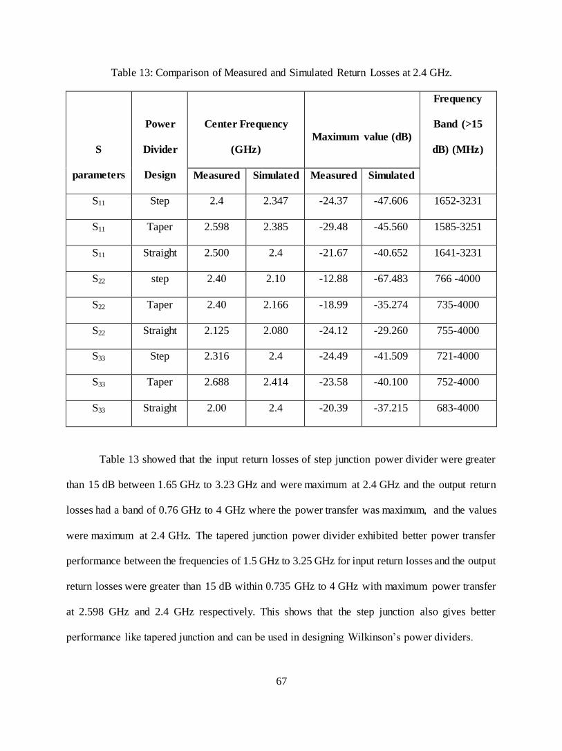
67
Table 13: Comparison of Measured and Simulated Return Losses at 2.4 GHz.
S
parameters
Power
Divider
Design
Center Frequency
(GHz)
Maximum value (dB)
Frequency
Band (>15
dB) (MHz)
Measured Simulated Measured Simulated
S11 Step 2.4 2.347 -24.37 -47.606 1652-3231
S11 Taper 2.598 2.385 -29.48 -45.560 1585-3251
S11 Straight 2.500 2.4 -21.67 -40.652 1641-3231
S22 step 2.40 2.10 -12.88 -67.483 766 -4000
S22 Taper 2.40 2.166 -18.99 -35.274 735-4000
S22 Straight 2.125 2.080 -24.12 -29.260 755-4000
S33 Step 2.316 2.4 -24.49 -41.509 721-4000
S33 Taper 2.688 2.414 -23.58 -40.100 752-4000
S33 Straight 2.00 2.4 -20.39 -37.215 683-4000
Table 13 showed that the input return losses of step junction power divider were greater
than 15 dB between 1.65 GHz to 3.23 GHz and were maximum at 2.4 GHz and the output return
losses had a band of 0.76 GHz to 4 GHz where the power transfer was maximum, and the values
were maximum at 2.4 GHz. The tapered junction power divider exhibited better power transfer
performance between the frequencies of 1.5 GHz to 3.25 GHz for input return losses and the output
return losses were greater than 15 dB within 0.735 GHz to 4 GHz with maximum power transfer
at 2.598 GHz and 2.4 GHz respectively. This shows that the step junction also gives better
performance like tapered junction and can be used in designing Wilkinson’s power dividers.
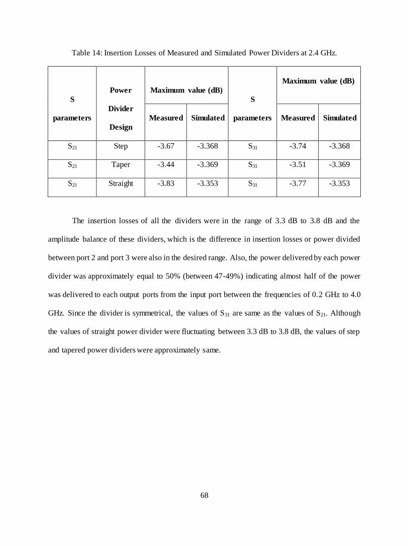
68
Table 14: Insertion Losses of Measured and Simulated Power Dividers at 2.4 GHz.
S
parameters
Power
Divider
Design
Maximum value (dB)
S
parameters
Maximum value (dB)
Measured Simulated Measured Simulated
S21 Step -3.67 -3.368 S31 -3.74 -3.368
S21 Taper -3.44 -3.369 S31 -3.51 -3.369
S21 Straight -3.83 -3.353 S31 -3.77 -3.353
The insertion losses of all the dividers were in the range of 3.3 dB to 3.8 dB and the
amplitude balance of these dividers, which is the difference in insertion losses or power divided
between port 2 and port 3 were also in the desired range. Also, the power delivered by each power
divider was approximately equal to 50% (between 47-49%) indicating almost half of the power
was delivered to each output ports from the input port between the frequencies of 0.2 GHz to 4.0
GHz. Since the divider is symmetrical, the values of S31 are same as the values of S21. Although
the values of straight power divider were fluctuating between 3.3 dB to 3.8 dB, the values of step
and tapered power dividers were approximately same.

69
Table 15: Comparison Between the Measured and Simulated Isolation of Power Dividers
S
parameters
Power
Divider
Design
Center Frequency
(GHz)
Maximum value (dB)
Frequency
Band (>15
dB) (MHz)
Measured Simulated Measured Simulated
S32 Step 2.342 2.419 -34.38 -45.279 1620-3190
S32 Taper 2.671 2.465 -43.10 -46.202 1650-3250
S32 Straight 2.603 2.496 -34.36 -51.235 1690-3301
It was observed from the table that the isolation was greater than 30 dB for all power
dividers and the step divider achieved an isolation of 34.38 dB, which is similar to the straight
divider. Also, it was observed from the table that the step and straight dividers had good isolation
results implying the coupling effects were negligible. Although tapered divider had better isolation
among the designs, the difference is minimum. Hence, it can see that the measured results were
meeting the desired performance of Wilkinson power divider with approximately similar results.
70
CHAPTER 5
CONCLUSION AND FUTURE SCOPE
This thesis was focused on two principal topics: The use of power combiners to extend the
range of Wi-Fi systems and to characterize RF power amplifiers (PAs) on break-out boards without
using solder to attach the PA thus allowing for rapid, high-volume characterization of commercial
PAs. For the main topic the focus was to simulate, design and test fabricated power dividers while,
for the PA testing topic, the goal was to deliver test data to Global ETS, Trinity FL, so that the
company could compare measured versus spec data to ensure that non-counterfeit devices were
delivered to one of their customers. In this chapter we will first summarize the results from the
thesis and then offer some suggestions for possible future work.
5.1 Conclusions
The results presented in Chapter Four indicated that different Wilkinson power divider
designs displayed similar performances at the same operating frequency when implemented using
microstrip technology. It was also noticed that the step divider had similar results as the straight
divider. Since the design and construction of the step divider was simpler, this design can be easily
fabricated in microwave industry. The design was robust and easy to use. All the fabricated power
dividers exhibited desired return losses greater than 15 dB, insertion losses of approximately 3.3
dB and isolation greater than 20 dB.
The coupling between the transmission lines also influences the odd and even mode
impedances of the transmission lines. This depends on the spacing between the transmission lines.
As the gap between these lines increases, the impedance varies due to the decrease in capacitance
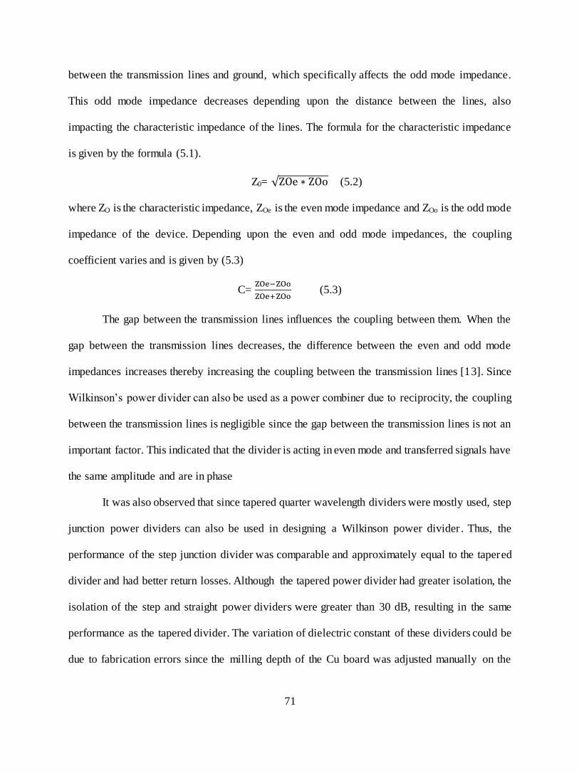
71
between the transmission lines and ground, which specifically affects the odd mode impedance.
This odd mode impedance decreases depending upon the distance between the lines, also
impacting the characteristic impedance of the lines. The formula for the characteristic impedance
is given by the formula (5.1).
Z0= √ZOe ∗ ZOo (5.2)
where ZO is the characteristic impedance, ZOe is the even mode impedance and ZOo is the odd mode
impedance of the device. Depending upon the even and odd mode impedances, the coupling
coefficient varies and is given by (5.3)
C= ZOe−ZOo
ZOe+ZOo (5.3)
The gap between the transmission lines influences the coupling between them. When the
gap between the transmission lines decreases, the difference between the even and odd mode
impedances increases thereby increasing the coupling between the transmission lines [13]. Since
Wilkinson’s power divider can also be used as a power combiner due to reciprocity, the coupling
between the transmission lines is negligible since the gap between the transmission lines is not an
important factor. This indicated that the divider is acting in even mode and transferred signals have
the same amplitude and are in phase
It was also observed that since tapered quarter wavelength dividers were mostly used, step
junction power dividers can also be used in designing a Wilkinson power divider . Thus, the
performance of the step junction divider was comparable and approximately equal to the tapered
divider and had better return losses. Although the tapered power divider had greater isolation, the
isolation of the step and straight power dividers were greater than 30 dB, resulting in the same
performance as the tapered divider. The variation of dielectric constant of these dividers could be
due to fabrication errors since the milling depth of the Cu board was adjusted manually on the
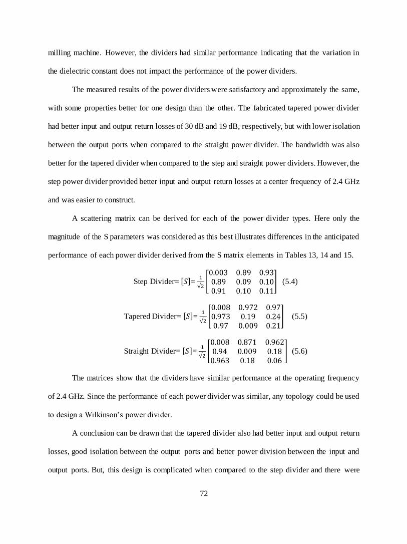
72
milling machine. However, the dividers had similar performance indicating that the variation in
the dielectric constant does not impact the performance of the power dividers.
The measured results of the power dividers were satisfactory and approximately the same,
with some properties better for one design than the other. The fabricated tapered power divider
had better input and output return losses of 30 dB and 19 dB, respectively, but with lower isolation
between the output ports when compared to the straight power divider. The bandwidth was also
better for the tapered divider when compared to the step and straight power dividers. However, the
step power divider provided better input and output return losses at a center frequency of 2.4 GHz
and was easier to construct.
A scattering matrix can be derived for each of the power divider types. Here only the
magnitude of the S parameters was considered as this best illustrates differences in the anticipated
performance of each power divider derived from the S matrix elements in Tables 13, 14 and 15.
Step Divider= [𝑆]= 1
√2[0.003 0.89 0.930.89 0.09 0.100.91 0.10 0.11
] (5.4)
Tapered Divider= [𝑆]= 1
√2[0.008 0.972 0.970.973 0.19 0.240.97 0.009 0.21
] (5.5)
Straight Divider= [𝑆]= 1
√2[0.008 0.871 0.9620.94 0.009 0.18
0.963 0.18 0.06] (5.6)
The matrices show that the dividers have similar performance at the operating frequency
of 2.4 GHz. Since the performance of each power divider was similar, any topology could be used
to design a Wilkinson’s power divider.
A conclusion can be drawn that the tapered divider also had better input and output return
losses, good isolation between the output ports and better power division between the input and
output ports. But, this design is complicated when compared to the step divider and there were

73
non-negligible variations between the simulated and experimental values when compared to the
step divider.
The designs were all compared, and it was deduced that any design can be implemented to
design a power divider with microstrip technology for a reasonable frequency under 10 GHz and
same performance can be expected from these dividers. Parallel dividers are equally efficient as
curved dividers and the parameters of the step junction power divider, tapered power divider and
straight power divider were similar. But step junction power divider was easy to manufacture and
could be understood easily.
5.2 Future Work
This section is divided into two parts: First a discussion of how power dividers can be used
to boost Wi-Fi signals without the use of RF repeaters, and second how the designs presented here
might be improved to achieve higher-performance Wilkinson power dividers.
5.2.1 Applications of Power Dividers in the RF and Microwave Industry
We know that power dividers are being used in the Wireless Industry for transmission and
receiving purposes in transceiver circuits, to boost the Wi-Fi signals, and to increase mobile signal
coverage in cellular repeater circuits. They can also be used for dual-band applications with broad
bandwidth and are also used in high power amplifier circuits. A power divider is also used in
WLAN applications to divide the input signals to feed an array of antennas. We can design 1:2N
power dividers, where N stands for the number of ports, which is used as a feed network for devices
like phase array antennas, RF communications, etc. Although we know that as the number of
output ports increases, isolation between them decreases so it is important that the desired isolation
of more than 15 dB criteria be maintained. A block diagram of N-way power dividers is shown in
the Figure 48, which can be used as a feeding circuit for many applications.
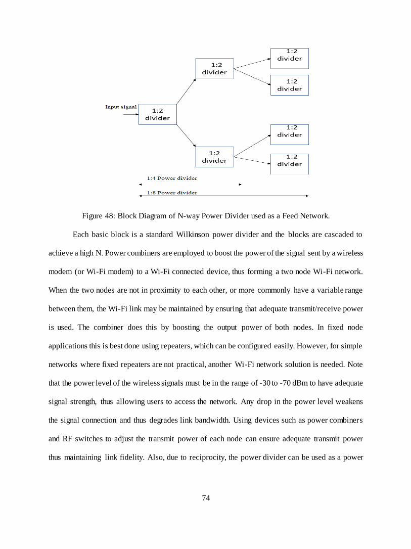
74
Figure 48: Block Diagram of N-way Power Divider used as a Feed Network.
Each basic block is a standard Wilkinson power divider and the blocks are cascaded to
achieve a high N. Power combiners are employed to boost the power of the signal sent by a wireless
modem (or Wi-Fi modem) to a Wi-Fi connected device, thus forming a two node Wi-Fi network.
When the two nodes are not in proximity to each other, or more commonly have a variable range
between them, the Wi-Fi link may be maintained by ensuring that adequate transmit/receive power
is used. The combiner does this by boosting the output power of both nodes. In fixed node
applications this is best done using repeaters, which can be configured easily. However, for simple
networks where fixed repeaters are not practical, another Wi-Fi network solution is needed. Note
that the power level of the wireless signals must be in the range of -30 to -70 dBm to have adequate
signal strength, thus allowing users to access the network. Any drop in the power level weakens
the signal connection and thus degrades link bandwidth. Using devices such as power combiners
and RF switches to adjust the transmit power of each node can ensure adequate transmit power
thus maintaining link fidelity. Also, due to reciprocity, the power divider can be used as a power

75
combiner. In this case the combiner has less losses when both output ports are driven with an equal
amplitude and at the same phase as shown in Figure 49.
Figure 49: Power Combiner/Divider in a Wi-Fi Transceiver Circuit to Boost the Wi-Fi Signals
and to Establish the Wi-Fi Link when the Transmitter/Receiver are Mobile.
5.2.2 Possible Power Divider Improvements
Although the dimensions of all the fabricated power divider boards were 4923 mm, more
compact divider boards are needed, and active research is going on to provide the desired
performance on compact fabricated boards [23]. Some of the new technologies for designing
Wilkinson’s power divider includes miniaturing the size while functioning in dual bands and using
stepped impedance lines and open stubs [24]. Also, other power combiners such as rat race
couplers can also be used to provide better power division with three (3) quarter wavelength
transmission lines (λ/4) and one (1) three quarter wavelength transmission line (3λ/4) with four
ports. Since the input ports do not have any lumped elements, the parasitic effects are less when
compared to the Wilkinson’s power divider [25]. The rat race couplers are used to combine two

76
in-phase signals with approximately no losses and to split the input signal without any phase
difference between the output ports. A typical rat race coupler is shown in Figure 50.
Figure 50: The Layout of a Typical Rat Race Coupler.
The input signal at Port 4 is divided into Ports 1 and 3while Port 2 is isolated. Hence, Port
4 is referred as sum port while Port 1 is the delta port. For an ideal rat race couplers, equal power
split of 3 dB is observed only at the operating frequency. Ports 2 and 4 has an 1800 phase difference

77
REFERENCES
[1] Keysight Technologies: Differences in Application Between Power Dividers and Power
Splitters
[2] Sardi, A., J. Zbitou, A. Errkik, L. E. Abdellaoui, A. Tajmouati, and M. Latrach. "A novel design
of a low-cost wideband Wilkinson power divider." Int. J. Electr. Comput. Energetic Electron.
Commun. Eng 9 (2015): 68-71.
[3] Rappaport, Theodore S. Wireless communications: principles and practice. Vol. 2. New Jersey:
prentice hall PTR, 1996.
[4] Tse, David, and Pramod Viswanath. Fundamentals of wireless communication. Cambridge
university press, 2005.
[5] Biswas, Subir, Raymond Tatchikou, and Francois Dion. "Vehicle-to-vehicle wireless
communication protocols for enhancing highway traffic safety." IEEE communications
magazine 44, no. 1 (2006): 74-82.
[6] Sobol, Harold. "Microwave industry outlook-microwaves for telecommunication
systems." IEEE transactions on microwave theory and techniques 50, no. 3 (2002): 1037-1038.
[7] Kamali, Behnam, Robert Alexander Bennett, and Dyani Camika Cox. "Understanding
WiMAX: An IEEE-802.16 standard-based wireless technology." IEEE Potentials 31, no. 5 (2012):
23-27.
[8] Dhawan, Sanjeev. "Analogy of promising wireless technologies on different frequencies:
Bluetooth, wifi, and wimax." In The 2nd International Conference on Wireless Broadband and
Ultra-Wideband Communications (AusWireless 2007), pp. 14-14. IEEE, 2007.

78
[9] Abdelrahman, Ramia Babiker Mohammed, Amin Babiker A. Mustafa, and Ashraf A. Osman.
"A Comparison between IEEE 802.11 n and ac Standards." (2015).
[10] Ferrante, Guido Carlo, Jocelyn Fiorina, and Maria-Gabriella Di Benedetto. "Robustness of
time reversal vs. all-rake transceivers in multiple access channels." arXiv preprint
arXiv:1405.4459 (2014).
[11] Yang, Fei, Cong Zhang, and Dan Li. "Design and implementation of a new wireless
microwave transceiver based on radio frequency technology." In 2017 IEEE 3rd Information
Technology and Mechatronics Engineering Conference (ITOEC), pp. 872-876. IEEE, 2017.
[12] Gherardi, Bancroft, and Frank B. Jewett. "Telephone repeaters." Proceedings of the American
Institute of Electrical Engineers 38, no. 11 (1919): 1255-1313.
[13] Pozar, David M. "Microwave engineering." Wiley (2012).
[14] Wentzel, Andreas, Viswanathan Subramanian, Ahmed Sayed, and Georg Boeck. "Novel
broadband Wilkinson power combiner." In 2006 European Microwave Conference, pp. 212-215.
IEEE, 2006.
[15] Berens, Logan J. "Design, analysis, and construction of an equal split Wilkinson power
divider." (2012).
[16] Stiles, J. "The Wilkinson power divider." University of Kansas, Dept. of EECS (2009).
[17] Noriega, Fernando, and Pedro J. González. "Designing LC Wilkinson power splitters." RF
interconnects/interfaces (2002): 18.
[18] An Introduction to Microwave Amplifiers Part 1: Microwave Amplifier Applications – Marki
Microwave RF & Microwave
[19] Understanding the Basics of Low-Noise and Power Amplifiers in Wireless Designs-Digi Key
[20] Kijanga, Peter. "Microwave Amplifiers Design." (2014).

79
[21] Shekhawat, Sampat S., John J. Dhyanchand, and John Horowy. "Darlington amplifier with
high speed turnoff." U.S. Patent 4,885,486 issued December 5, 1989.
[22] Pathak, Rashmi. "Characterizing losses in microstrip transmission lines." University of
Wisconsin–Madison (2005).
[23] Deng, Pu-Hua, and Yu-Ta Chen. "New Wilkinson power dividers and their integration
applications to four-way and filtering dividers." IEEE Transactions on Components, Packaging
and Manufacturing Technology 4, no. 11 (2014): 1828-1837.
[24] Deng, Pu-Hua, Jin-Hao Guo, and Wen-Chi Kuo. "New Wilkinson power dividers based on
compact stepped-impedance transmission lines and shunt open stubs." Progress In
Electromagnetics Research 123 (2012): 407-426.
[25] Cheng, K-KM, and Fai-Leung Wong. "A novel rat race coupler design for dual-band
applications." IEEE Microwave and Wireless Components Letters 15, no. 8 (2005): 521-523.