rf circuits – design & analysis - smdpii-vlsi:special...
TRANSCRIPT

Dr. T. K. Bhattacharyya,Dept. of E&ECE
RF Circuits –Design & Analysis
Dr. T K BhattacharyyaDr. T K Bhattacharyya
E & ECE Dept.IIT Kharagpur..

Dr. T. K. Bhattacharyya,Dept. of E&ECE
Basics of RF
Dr. T. K. Bhattacharyya,Dept. of E&ECE
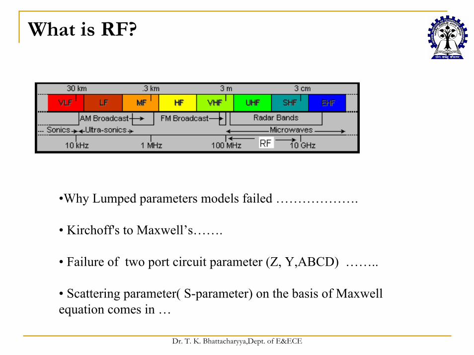
What is RF?
•Why Lumped parameters models failed ……………….
• Kirchoff's to Maxwell’s…….
• Failure of two port circuit parameter (Z, Y,ABCD) ……..
• Scattering parameter( S-parameter) on the basis of Maxwell equation comes in …

Dr. T. K. Bhattacharyya,Dept. of E&ECE
Application area of the RF-IC designer
•Wireless communication
•Radar
•Navigation
•Remote sensing
•RF identification
•Automobile and Highways
•Sensors:
•Medical
•Radio- astronomy and space exploration
Dr. T. K. Bhattacharyya,Dept. of E&ECE
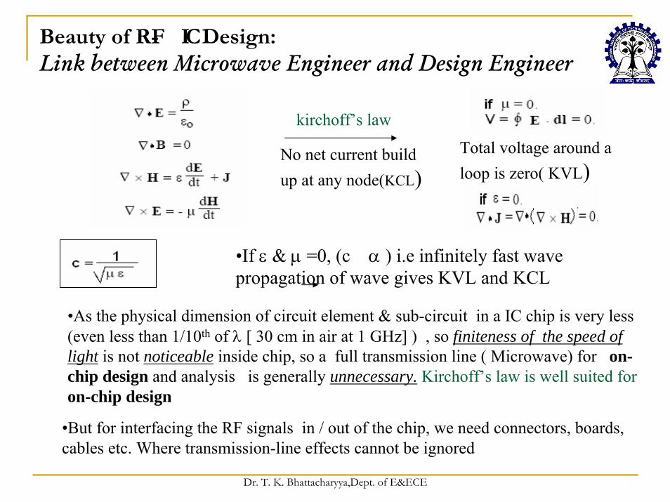
Beauty of RF- IC Design: Link between Microwave Engineer and Design Engineer
kirchoff’s law
Total voltage around a loop is zero( KVL)
No net current build up at any node(KCL)
•If ε & μ =0, (c α ) i.e infinitely fast wave propagation of wave gives KVL and KCL
•As the physical dimension of circuit element & sub-circuit in a IC chip is very less (even less than 1/10th of λ [ 30 cm in air at 1 GHz] ) , so finiteness of the speed of light is not noticeable inside chip, so a full transmission line ( Microwave) for on-chip design and analysis is generally unnecessary. Kirchoff’s law is well suited for on-chip design
•But for interfacing the RF signals in / out of the chip, we need connectors, boards, cables etc. Where transmission-line effects cannot be ignored

Dr. T. K. Bhattacharyya,Dept. of E&ECE
Comparison of Analog and RF/MW
( Analog [Low frequency<100MHz] ) ( RF/MW[ High frequency>100MHz] )
Conductor
Capacitor
Resistor
Inductor
Simple wire
Microstrip line
Ceramic
Carbon Thin Film SMD comp.
Thin Film SMD comp.
Wire Wound
Thin Film SMD comp.
1. On Discrete PCB component

Dr. T. K. Bhattacharyya,Dept. of E&ECE
Comparison of Analog and RF/MW
( Analog [Low frequency<100MHz] ) ( RF/MW [High frequency>100MHz] )
1. On Performance Based
A. Small signal AC equivalent circuit analysis
B. Linearity
C. Stability
D. Noise (on few cases)
A. Small signal AC equivalent circuit analysis with parasitic i.e. Good circuit Modeling
B. Matching
E. Linearity
D. Stability
C. Noise
F. Sensitivity
G. Dynamic range

Dr. T. K. Bhattacharyya,Dept. of E&ECE
RF Circuit & Systems – Design IssuesPhase shift of the signal is significant over the extent of the component because it’s size is comparable with the wavelength.
The reactance of the circuit must be accounted for, particularly those associated with the parasitic of the active devices.
Circuit losses causes degradation of Q, reduction of frequency selectivity and noise performance.
Noise especially arising from the circuit can be significant and it’s effect needs to be modeled.
Electromagnetic radiation capacitive coupling and substrate coupling significantly alter the performance of the circuit.
Reflection issues, because circuit size is of the order of a wavelength.
Circuit design should take care to ensure reflections do not cause any loss of gain, power, or failure of components.
Nonlinearity which causes distortion and unwanted frequency components is undesirable, but it may become essential part of the circuit operation, as in mixing or local oscillators.

Dr. T. K. Bhattacharyya,Dept. of E&ECE
High Frequency Device modeling
Silicon Technologies
BiCMOS MOSBipolar
Junction Isolated
BJTs
DielectricIsolated
PMOS NMOS
CMOS

Dr. T. K. Bhattacharyya,Dept. of E&ECE
High Frequency Device modeling (contd.)Visualization of Process Flow
Protective Overcoat
CVD Oxide
p-epi
p-substrate
n+ n+
Gate oxidepolyFOX
contact
Metal-1
via
Metal-2

Dr. T. K. Bhattacharyya,Dept. of E&ECE
Standard Digital CMOS is hardly the ideal medium for RF ICs, because of :Lossy Silicon substrateLarge source/drain parasiticsHigh device noise and poor 1/f noise performanceSeries gate resistance
But,Device scaling …faster CMOS fT (and fmax) ….range of 60GHz doubles roughly every 3 years.CMOS is cost effectiveBoth digital & analog block can be designed on same substrateHigh linearity; Low distortionLow power consumptionOn-chip realization of passive inductors and capacitors
CMOS BJT
Symmetric behavior.
Better linearity (Higher signal swing).
Higher fT at sub-micron feature size.
Better scaling properties.
Low power (no gate DC current).
Higher gm for same bias.
High fT.
Low thermal and 1/fnoise, but input current noise.
Lower DC offset .
No body effect.
Lower overdrive (Low VCE sat).
WHY CMOS FOR RF-IC?

Dr. T. K. Bhattacharyya,Dept. of E&ECE
R
RRpoly Cgs Cgd Cds
Csub
•To calculate magnetic coupling between two adjacent metal line, interlayer capacitance , EMI between subcircuits & on-chip passive component (such as inductor and MIM capacitor) , the Maxwell EM equation is required ( Challenging issue !!!)

Dr. T. K. Bhattacharyya,Dept. of E&ECE
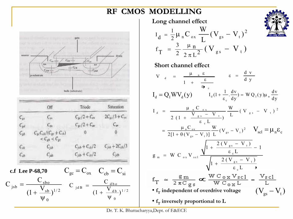
RF CMOS MODELLING
Maximum unit power gain Maximum unit power gain frequencyfrequency
Maximum CutMaximum Cut--off frequencyoff frequency
““Standard” (digital oriented) MOS models do not allow for RFStandard” (digital oriented) MOS models do not allow for RF
In RF, Cgs ( whose effect negligible in low frequency analog) affects the matching with
successive blocks . Frequency dependence of Transconductance(gm )
Dr. T. K. Bhattacharyya,Dept. of E&ECE
c.f Lee P-68,70 gc oxC C= cb siC C=sbo
jsb1/ 2sb
0
CC V(1 )=
+ψ
d b oj d B
1 / 2d b
0
CC V(1 )=
+ψ
Long channel effect
n ox gs t21
Id 2WC (V V )L
= μ −
g s t3 nf T 22 2 L
( V V )μ=
π−
Short channel effectn
d
c
V1
μ ε=
ε+
ε
d vd y
ε =
d I dI Q WV (y)=,
d I nc
1 dv dvI (1 . ) W Q ( y)dy dy
+ = με
n o xd g s t
g s t
c
2C WI ( V V )V V L2 ( 1 )L
μ= −
−+
εn o x
g s tg s t
2C W ( V V )2[1 ( V V )] L
μ= −
+ θ −
g s t
cm o x s c l
g s t
c
2 ( V V )1 1
Lg W C V
2 ( V V )1
L
−+ −
ε=
−+
ε
scl n cV = μ ε
,
• fT independent of overdrive voltagegs t(V V )−
• fT inversely proportional to L
RF CMOS MODELLINGRF CMOS MODELLING

Dr. T. K. Bhattacharyya,Dept. of E&ECE
Noise
• Thermal Noise-Brownian motion of thermally agitated charge carriers - generated in every physical resistor
- pure reactive components generate no thermal noise
Thermal Noise in MOSFETTh most significant source of noise Channel Noise:
In2 = 4kTγgm
• γ ~1 at a zero VDS for long channel device, 2/3 at saturation, 2-3 for short channel transistor
Significance :The significance of noise performance of a circuit is the limitation it places on thesmallest input signals(MDS) the circuit can handle before the noise degrades the quality of output signal.
Dr. T. K. Bhattacharyya,Dept. of E&ECE
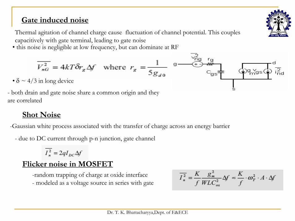
• this noise is negligible at low frequency, but can dominate at RF
• δ ~ 4/3 in long device
- both drain and gate noise share a common origin and they are correlated
Shot Noise-Gaussian white process associated with the transfer of charge across an energy barrier
- due to DC current through p-n junction, gate channel
Flicker noise in MOSFET-random trapping of charge at oxide interface- modeled as a voltage source in series with gate
Gate induced noise
Thermal agitation of channel charge cause fluctuation of channel potential. This couples capacitively with gate terminal, leading to gate noise

Dr. T. K. Bhattacharyya,Dept. of E&ECE
Noise figureNoise figure (cont..)Noise figure of cascaded stages ..
For two stage case it can be shown
For m- stages
• NF of each stages is calculated with respect to the output impedance of previous stages
• The noise is contributed by each stage decreases as the gain preceding the stages increase
•That’s why the first stage of any system should have higher gain with low noise figure ( PRIME CRITERION FOR LOW NOISE AMPLIFIER (LNA) DESIGN OF A RECEIVER)
Dr. T. K. Bhattacharyya,Dept. of E&ECE
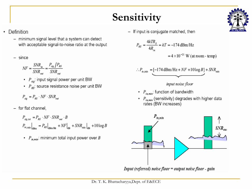
Sensitivity

Dr. T. K. Bhattacharyya,Dept. of E&ECE
Dynamic Range

Dr. T. K. Bhattacharyya,Dept. of E&ECE
Modeling of Arbitrary ShapedRF Spiral Inductors for Circuit Simulation
Complex field coupling between turns.
For on- chip spiral inductor the following difficulties arise due to conductive substrate:
1) Eddy current in the substrate 2) Coupling between field generated by the coil and field
generated by the eddy current. This mutual coupling increases the active part of the current and as a result Q decreases.Proposing a New Generic Methodology of Modeling RF Spiral Inductor for Circuit Simulation.Developing a System Identification Algorithm for the proposed modeling technique.
Dr. T. K. Bhattacharyya,Dept. of E&ECE
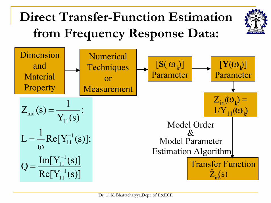
Direct Transfer-Function Estimation from Frequency Response Data:
Dimension and
Material Property
Numerical Techniques
or Measurement
Transfer Function (s)
[S( )] Parameter
Model Order &
Model Parameter
[Y( )] Parameter
Zin( ) = 1/Y11( )
Estimation Algorithm
kω kω
kωkω
inZ
ind11
111
111
111
1Z (s) ;Y (s)
1L Re[Y (s)];
Im[Y (s)]QRe[Y (s)]
−
−
−
=
=ω
=

Dr. T. K. Bhattacharyya,Dept. of E&ECE
The basic Idea
Both model order and model parameters are identified with PSO.
Two independent PSO has been used.
One PSO has been used for model parameter Estimation for a given model order.
Another PSO has been used for model order Estimation.

Dr. T. K. Bhattacharyya,Dept. of E&ECE
Case Study ITABLE I
Dimensions Of The Inductor Used In Case Study I
Outer Diameter (μm) 120
Metal Width; Metal Spacing (μm) 5.5; 3
No. of Turns 6
Metal Layer; Under Pass M6; M5

Dr. T. K. Bhattacharyya,Dept. of E&ECE
TABLE IIParameters Of The Estimated Transfer Function
K (Gain) 1.5771039E-10
Z1 (1st Zero) 1.0146618E+9
Z2 (2nd Zero) 1.2566E+13
P (Pole) 8.6472026E+11
Dr. T. K. Bhattacharyya,Dept. of E&ECE
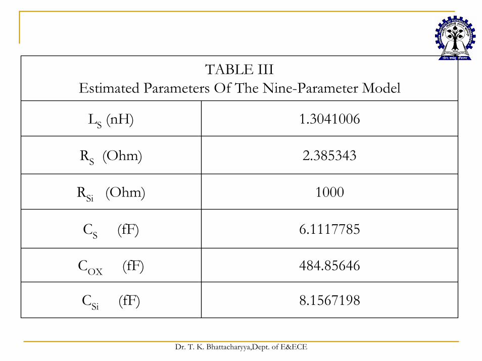
TABLE IIIEstimated Parameters Of The Nine-Parameter Model
LS (nH) 1.3041006
RS (Ohm) 2.385343
RSi (Ohm) 1000
CS (fF) 6.1117785
COX (fF) 484.85646
CSi (fF) 8.1567198
Dr. T. K. Bhattacharyya,Dept. of E&ECE
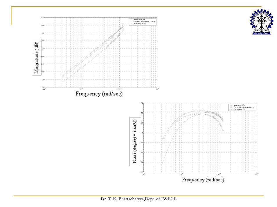
109
1010
1011
1012
10
15
20
25
30
35
40
45
50
55
Frequency (rad/sec)
Mag
nitu
de (
dB)
Measured ZinZin of 9 Parameter ModelEstimated Zin
109
1010
1011
1012
55
60
65
70
75
80
85
90Measured ZinZin of 9 Parameter ModelEstimated Zin

Dr. T. K. Bhattacharyya,Dept. of E&ECE
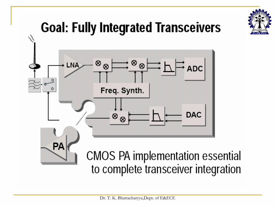
RF Transceiver Design

Dr. T. K. Bhattacharyya,Dept. of E&ECE
From System level to Component level specifications (contd.)
Sensitivity of the Receiver
Block Diagram of the Receiver System
Dr. T. K. Bhattacharyya,Dept. of E&ECE
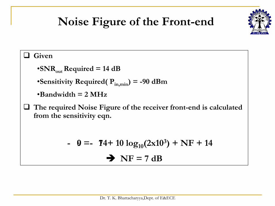
Noise Figure of the Front-end
Given
•SNRout Required = 14 dB
•Sensitivity Required( Pin,min) = -90 dBm
•Bandwidth = 2 MHz
The required Noise Figure of the receiver front-end is calculated from the sensitivity eqn.
- 90 = - 174+ 10 log10(2x10³) + NF + 14
NF = 7 dB

Dr. T. K. Bhattacharyya,Dept. of E&ECE
Gain, NF and IIP3 of cascaded stages
Total Noise Factor
Total IIP3
p1 p2 pkA A AAp = × × ×L
32 k1
p1 p1 p2 p1 p2 p(k-1)
NF 1NF 1 NF 1NF=NF .....A A A A A ...A
−− −+ + + +
p1 p1 p2 p1 p2 p(k-1)
3 3,1 3,2 3,3 3,k
A A A A A ...A1 1= .....IIP IIP IIP IIP IIP
+ + + +
Total Gain
Where NFi, Api and IIP3,i are respectively Noise Factor , Available Power Gain and input 3rd order intercept point of the i-th stage

Dr. T. K. Bhattacharyya,Dept. of E&ECE
Example- Gain and NF calculation
Dr. T. K. Bhattacharyya,Dept. of E&ECE
RF Transceiver Design:Low Noise Amplifiers
Dr. T. K. Bhattacharyya,Dept. of E&ECE
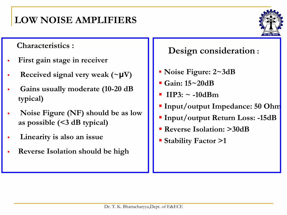
LOW NOISE AMPLIFIERS
Characteristics :
First gain stage in receiver
Received signal very weak (~μV)
Gains usually moderate (10-20 dB typical)
Noise Figure (NF) should be as low as possible (<3 dB typical)
Linearity is also an issue
Reverse Isolation should be high
Noise Figure: 2~3dB
Gain: 15~20dB
IIP3: ~ -10dBm
Input/output Impedance: 50 Ohm
Input/output Return Loss: -15dB
Reverse Isolation: >30dB
Stability Factor >1
Design consideration :

Dr. T. K. Bhattacharyya,Dept. of E&ECE
Different structure of CMOS LNA
All structures are narrow-band
Common source LNACommon source LNA ac equivalent modelac equivalent model
Capacitive input impedance.Lg cancels Capacitive term.A parallel RS (50 Ω) is added to match input source R50.
To reduce the effect of Zout (img)on tuning circuit, C value should be large compared to Zout
Corresponding circuit
Disadvantage of this circuit :
Due to Rextra , the power divide by 2.
NF ~1+ (γ/α) * Rextra/R50 , γ & α (=gm/gdo) are device parameter. NF~3-4 dB.
Due to Cgd reverse isolation(S11) Bad.
Cgd affects stability due to presence of zero in transfer function (Vout/Vin)
Dr. T. K. Bhattacharyya,Dept. of E&ECE
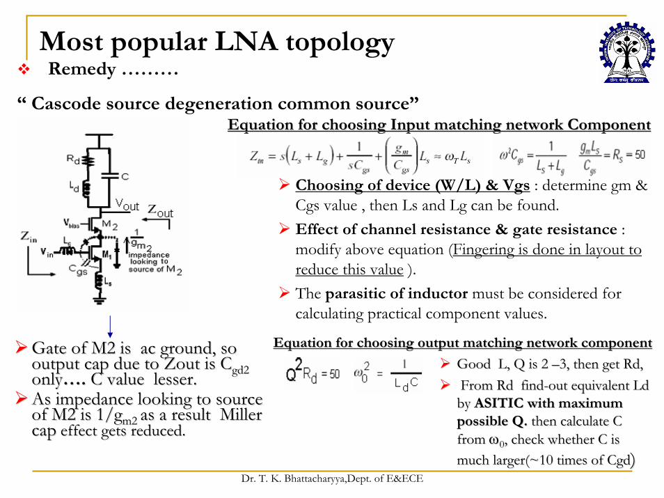
Most popular LNA topologyRemedy ………
“ Cascode source degeneration common source”Equation for choosing Input matching network ComponentEquation for choosing Input matching network Component
Choosing of device (W/L) & Vgs : determine gm & Cgs value , then Ls and Lg can be found.Effect of channel resistance & gate resistance : modify above equation (Fingering is done in layout to reduce this value ).The parasitic of inductor must be considered for calculating practical component values.
Equation for choosing output matching network componentEquation for choosing output matching network componentGate of M2 is ac ground, so Gate of M2 is ac ground, so output cap due to Zout is Coutput cap due to Zout is Cgd2gd2onlyonly….…. C value lesser.C value lesser.As impedance looking to source As impedance looking to source of M2 is 1/gof M2 is 1/gm2 m2 as a result Miller as a result Miller capcap effect gets reduced.effect gets reduced.
Good L, Q is 2 Good L, Q is 2 ––3, then get Rd, 3, then get Rd, From Rd findFrom Rd find--out equivalent Ld out equivalent Ld by by ASITIC with maximum ASITIC with maximum possible Q.possible Q. then calculate C then calculate C from from ωω00, check whether C is , check whether C is much larger(~10 times of much larger(~10 times of CgdCgd))

Dr. T. K. Bhattacharyya,Dept. of E&ECE
1 V Low Noise Amplifier
Performance Parameters
Values in the typical corner
Supply Voltage 1 Volt
Bandwidth 825 - 975 MHz
Voltage Gain 16.53 dB
Power Consumption 4.06 mW
Noise Figure 2.327 dB
Native MOSes used to facilitate low voltage operationThe input N/W consisting of LG and CGS is tuned to
900 MHz.The LC load is also tuned to 900 MHz.Gate induced noise is included in simulation by an
equivalent resistor.
Schematic

Dr. T. K. Bhattacharyya,Dept. of E&ECE
Subthreshold RF Design:Multiband & Wideband Applications

Dr. T. K. Bhattacharyya,Dept. of E&ECE
Introduction
Major challenges in VLSI Design:Power Consumption.Performance (Speed/Area).Reliability.
Subthreshold region designWeak inversion MOSFET provides sufficient transconductance.
Very low power consumption.Major RF Front-end modules
Low Noise Amplifier (LNA)Voltage Controlled Oscillator (VCO)
Dr. T. K. Bhattacharyya,Dept. of E&ECE
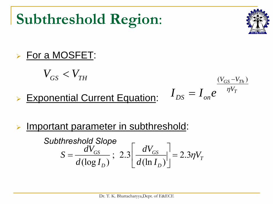
Subthreshold Region:
For a MOSFET:
Exponential Current Equation:
Important parameter in subthreshold:Subthreshold Slope
GS THV V<
2.3 2.3(log ) (ln )
GS GST
D D
dV dVS Vd I d I
η⎡ ⎤
= =⎢ ⎥⎣ ⎦
;
( )GS Th
T
V VV
DS onI I e η−
=

Dr. T. K. Bhattacharyya,Dept. of E&ECE
Single Band LNAInput Impedance (in saturation):
Tune gm or LS:Real Part = 50 Ω
Imaginary Part = 0
Input Matching :Pad-Pin parasitics modify input impedance.Separate off-chip matching network required.Matching needed over a bandwidth – Q based matching.
Zin
Iout1m s
in sgs gs
g LZ sLC sC
= + +
LNA input Device

Dr. T. K. Bhattacharyya,Dept. of E&ECE
Subthreshold Operation and Modeling
Accurate input impedance modeling:Closed Form expression of input impedance.Automatic generation of Q-based matching network.
Effect of parasitic capacitors Device capacitors play a major role.Channel not fully formed.Gate-to-Bulk & Source-to-Bulk capacitors

Dr. T. K. Bhattacharyya,Dept. of E&ECE
Subthreshold Operation and Modeling (Contd.)
Lpin Lbond
LS
RSS
M1
M2
LC
R
CpadCframe
Vout
Zin
Schematic of packaged cascode LNA

Dr. T. K. Bhattacharyya,Dept. of E&ECE
Subthreshold Operation and Modeling (Contd.)
+
- +
-
Lpin Lbond
Cframe Cpad Cgb1 Vgs1
Cgd1
Cgs1
gm1Vgs1
Csb1Ls
RS
gm2Vgs2
Vgs2 Cgs2+Csb2+Cdb1
Cout
ZL
Vx
V0V1
Modified Subthreshold region model of LNA input
Dr. T. K. Bhattacharyya,Dept. of E&ECE
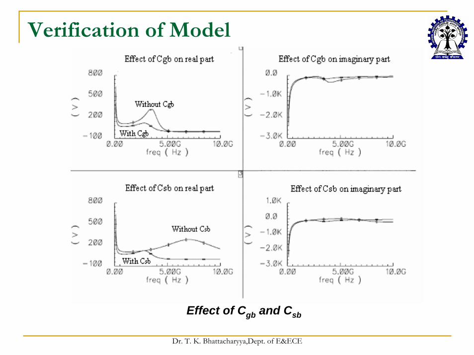
Verification of Model
Effect of Cgb and Csb

Dr. T. K. Bhattacharyya,Dept. of E&ECE
Verification of Model (Contd.)
Model and simulation results coincide

Dr. T. K. Bhattacharyya,Dept. of E&ECE
Q-based input matching
Matching over a bandwidth:Bandwidth defined by Quality Factor (Q)
Conventional techniques:and T matching techniques.
0fQf
=Δ
π L
C1 C2RL RL
L1 L2
C
match T matchπ

Dr. T. K. Bhattacharyya,Dept. of E&ECE
π match network analysis
Variation of matching components with frequency

Dr. T. K. Bhattacharyya,Dept. of E&ECE
π match network analysis (contd.)
Variation of matching components with LS
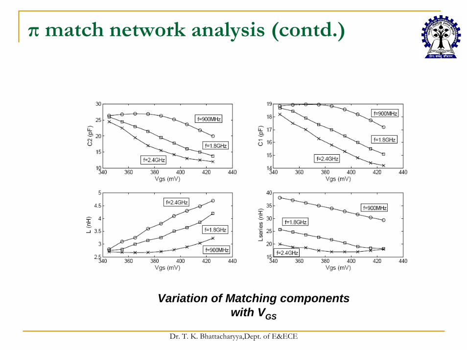
Dr. T. K. Bhattacharyya,Dept. of E&ECE
π match network analysis (contd.)
Variation of Matching components with VGS

Dr. T. K. Bhattacharyya,Dept. of E&ECE
Effect of Finite component Q
Severe degradation of matching performance
S11 for ideal case and Q=30
Dr. T. K. Bhattacharyya,Dept. of E&ECE
Limitations of Conventional Approach
Unsymmetrical profile for S11 over the bandwidth.
Similar problems with Real and Imaginary part of input impedance.
Effect prominent at lower frequency bands [GSM band (900MHz)].

Dr. T. K. Bhattacharyya,Dept. of E&ECE
PSO Based Matching Technique
Based on Particle Swarm OptimizationHeuristic method.Based on flocking of birds/swarms.Reaches optimum by modifying velocity of each particle.
PSO based approach applied to Q-based matching
Desired Real part profile -

Dr. T. K. Bhattacharyya,Dept. of E&ECE
PSO Based Matching Technique (Contd.)
Equations Optimized :
1 | Re( @850 ) 35 | | Im( @850 ) |in inf Z MHz Z MHz= − +
2 | Re( @950 ) 35| | Im( @950 ) |in inf Z MHz Z MHz= − +
3 | Re( @900 ) 50 | | Im( @900 ) |in inf Z MHz Z MHz= − +
1 1 2 2 3 3optf w f w f w f= + +
Wi’s are weights of fi. Weight of function at 900MHz was maximum

Dr. T. K. Bhattacharyya,Dept. of E&ECE
Results of PSO Based matching

Dr. T. K. Bhattacharyya,Dept. of E&ECE
Concurrent Dual-band LNA
Existing technique (Hashemi):Cancellation of imaginary part at2 frequencies using LC tank network
Real Part = made 50 Ω by adjustinggm and LS.
Lbond
LS
RSS
M1
M2
LC
R
Vout
Zin
Lg
Cg
Sm
gs
LgC
Dr. T. K. Bhattacharyya,Dept. of E&ECE
Concurrent Dual-band LNA (Contd.)
Drawbacks of existing technique:
Pad/Pin parasitics severely influence both real and imaginary part of input impedance.
Input matching is only at 1 frequency, i.e. not Q-based over a bandwidth.
Value of LS required for input match is generally very high at lower center frequencies.

Dr. T. K. Bhattacharyya,Dept. of E&ECE
Proposed PSO based matching
LNA input impedance at 2 predefined frequencies
Matching network value for 2 frequencies
Unity Current Source
Q-based pi match
Select Network topology for each pi element
LC tank, LC series, combination, etc
Calculation of network values

Dr. T. K. Bhattacharyya,Dept. of E&ECE
Results of dual-band matching
Accurate input match at both frequencies (900MHz and 1.8GHz)

Dr. T. K. Bhattacharyya,Dept. of E&ECE
Finite Q effect
Finite Q of components affect matching performance.
Individual networks have different effects on final input match.
Lseries and C1 component finite Q have minimal effect on matching performance.
Dr. T. K. Bhattacharyya,Dept. of E&ECE
RF Transceiver Design:Mixers
Dr. T. K. Bhattacharyya,Dept. of E&ECE
Mixer
Mixers Indispensable components of transceiversUsed to up-convert or down-convert a baseband signal to/from the carrier frequency Basic philosophy behind mixing is MULTIPLICATIONSay we have 2 frequencies f1 and f2, then cos 2πf1t and cos 2πf2t are the 2 signals
Multiplying them gives evidently the f1-f2 and the f1+f2 components, out of which, one we select through filtering

Dr. T. K. Bhattacharyya,Dept. of E&ECE
Downconversion Mixers
The most basic Downconversion mixer is the Gilbert cell mixer
RF signal: Radio Frequency signalLO signal: Local Oscillator signalVout gives the IF or the Intermediate frequency signal

Dr. T. K. Bhattacharyya,Dept. of E&ECE
Basic terms associated with mixing
Conversion Gain: Gc= VIF/VRF=> the 2 signals are evidently at 2 different frequenciesNoise Figure (in dB): S/N ratio at IF output port –S/N ratio at RF output port
NFSSB= NFDSB + 3dBLinearity: 1dB compression point, IIP2 and IIP3 shown as

Dr. T. K. Bhattacharyya,Dept. of E&ECE
Gilbert Mixer…… analyzed
Approximating the LO signal as a square waveGc = gmRL
Noise figure is typically of the order of 10-15dB
The main catch, however, is in the DC offset arising from the low LO-RF isolation as shown.
2π

Dr. T. K. Bhattacharyya,Dept. of E&ECE
Hmmm….so?
The problem of DC offset arising out of poor LO-RF isolation can pose serious problems by saturating the IF stage The problem arises simply because the LO and the RF bands lie in such close proximity in the frequency spectrum
……………..What if we mix LO(=RF/2) with RF instead of RF with LO=RF?This is precisely what we mean by even harmonic mixing

Dr. T. K. Bhattacharyya,Dept. of E&ECE
Even Harmonic Mixing
Harmonic mixer suppresses the fundamental mixing between the signal and LO
It allows mixing of the signal with the harmonics of LO
Dr. T. K. Bhattacharyya,Dept. of E&ECE
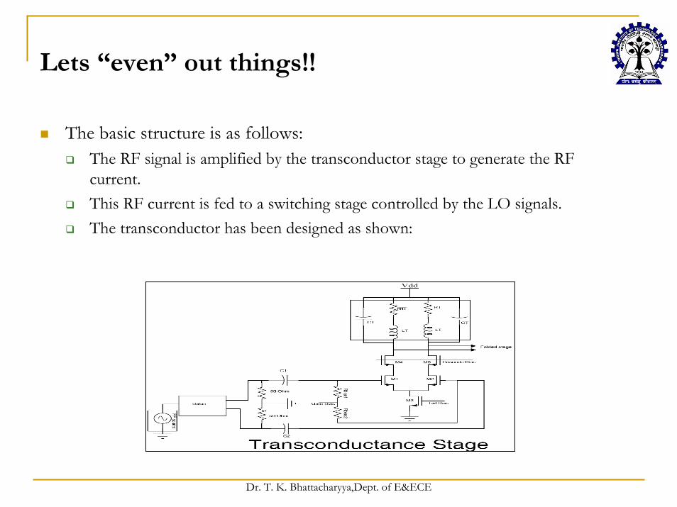
Lets “even” out things!!
The basic structure is as follows:The RF signal is amplified by the transconductor stage to generate the RF current.This RF current is fed to a switching stage controlled by the LO signals. The transconductor has been designed as shown:

Dr. T. K. Bhattacharyya,Dept. of E&ECE
Let’s “even” out things (2)
The LO-controlled switching stage is as shown:
The LO signals are applied in quadrature mode i.e. each one is 90° phase-shifted from the other.

Dr. T. K. Bhattacharyya,Dept. of E&ECE
Let’s “even” out things(3)
The quadrature LO signals are applied in an AND-OR mode as shown in the switching stage resulting in a frequency doubling as shown diagrammatically
AND
OR

Dr. T. K. Bhattacharyya,Dept. of E&ECE
RF Transceiver Design:Frequency Synthesizers

Dr. T. K. Bhattacharyya,Dept. of E&ECE
Frequency Synthesizer Block Diagram
PLL-based Frequency Synthesizer consists-Phase Frequency Detector (PFD)Charge Pump (CP)Loop Filter (LF)Voltage Control Oscillator (VCO)Frequency Divider
Integer N Divider (Integer N Frequency Synthesizer)Fractional N Divider (Fractional N Frequency Synthesizer)
Block Diagram of Frequency SynthesizerBlock Diagram of Frequency Synthesizer
OUTPUT FREQUENCYPFD CHARGE
PUMPLOOP
FILTER
VCO
FREQUENCYDIVIDER
REFERENCE FREQUENCY
Channel Control

Dr. T. K. Bhattacharyya,Dept. of E&ECE
Open loop
Closed loop
sK
sKK vd =
Ks /11
+That is fine for small signal linear control loopBut large signal(bias) output of PD may not be directly compatible withVCO input. Need gain/attenuation/shift/filtering: Loop filter
Normally vp is discrete(like PWM)Required vo is steady (DC)vp can be converted to vo by simple LPF
Discrete nature of PD (and vp) can be treated by continuous linear loopif bandwidth of the loop is within 1/10-th of the frequency of vp
fIN +fOUT
-PD VCO 1/s
w
fIN +fOUT
-PD VCO 1/s
wKh
Basic PLL
vp vovp vo
Kh
Dr. T. K. Bhattacharyya,Dept. of E&ECE
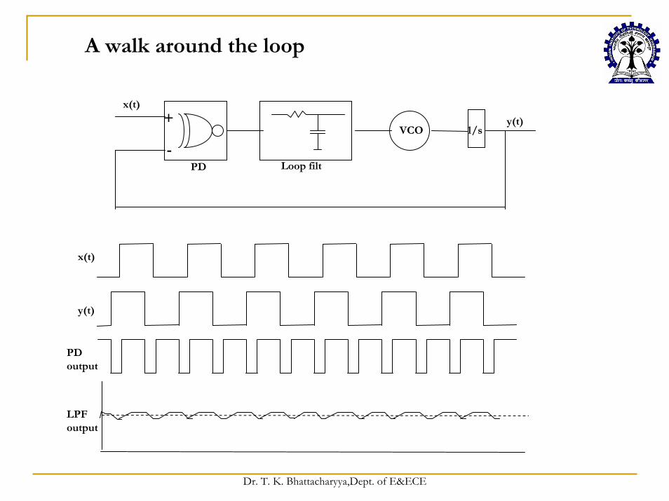
x(t)
y(t)
PD output
LPFoutput
+
-PD
VCO 1/s
Loop filt
x(t)
y(t)
A walk around the loop
Dr. T. K. Bhattacharyya,Dept. of E&ECE
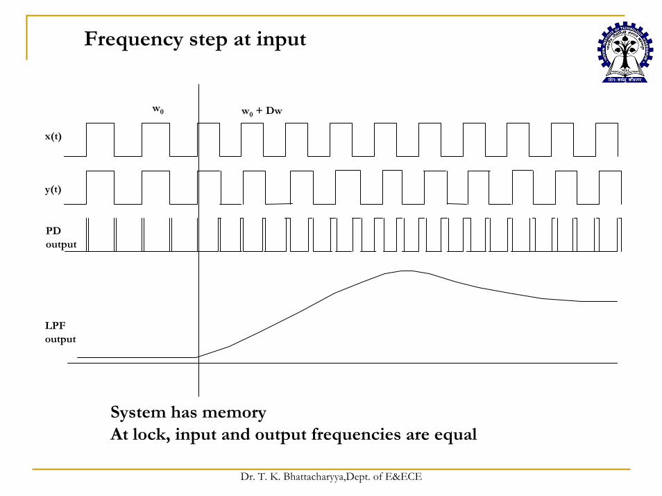
w0 w0 + Dw
System has memoryAt lock, input and output frequencies are equal
x(t)
y(t)
PD output
LPFoutput
Frequency step at input
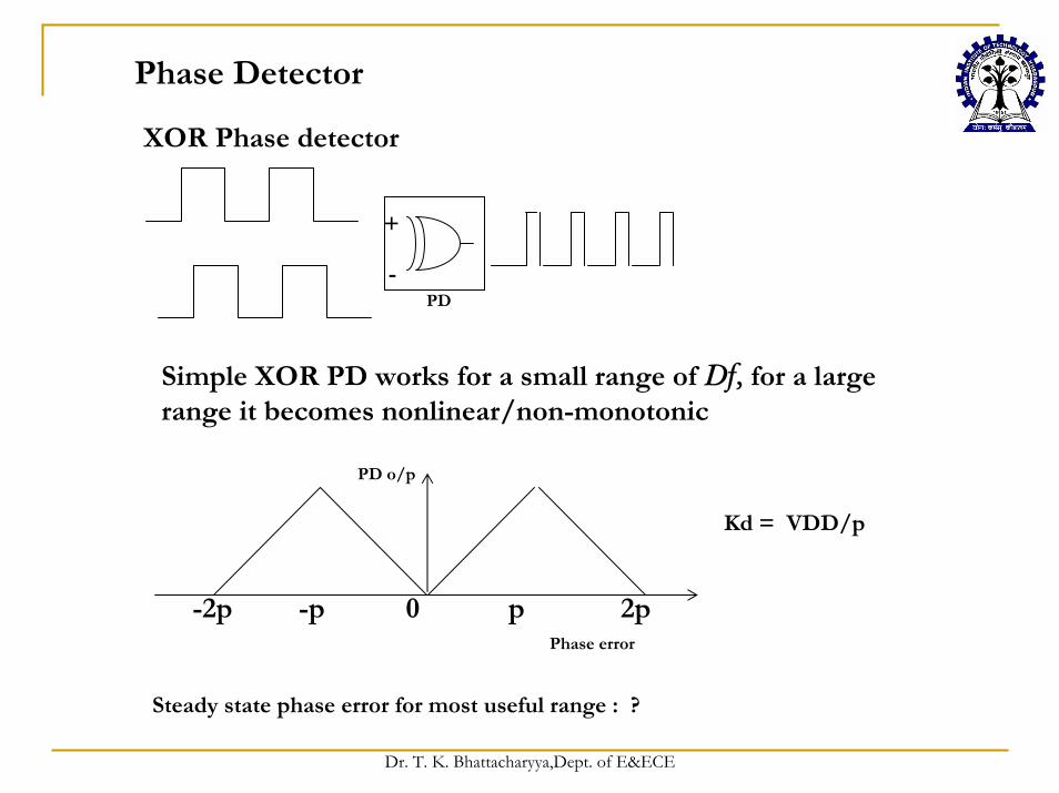
Dr. T. K. Bhattacharyya,Dept. of E&ECE
Simple XOR PD works for a small range of Df, for a large range it becomes nonlinear/non-monotonic
-2p -p 0 p 2p
+
-PD
Phase Detector
Phase error
PD o/p
XOR Phase detector
Kd = VDD/p
Steady state phase error for most useful range : ?

Dr. T. K. Bhattacharyya,Dept. of E&ECE
Phase Detector
Sequential Phase detector (SR flip-flop)
x(t)
y(t)
o/p
Kd = VDD/2pMost useful range offered when Df = p : cannot use for 0 steady state phase error
Df
-4p -2p 0 2p 4p
x(t) set
y(t) reset o/p
VDD

Dr. T. K. Bhattacharyya,Dept. of E&ECE
Phase Frequency Detector (PFD)
Three-state state machine representation
Output UP and DN pulses
x(t)
y(t)
up
dn
x(t)
y(t)
up
dn
+
-PFD
x(t)
y(t)
up
dn
Create down pulse
All reset Create up pulse
x(t) rising edge x(t) rising edge
y(t) rising edge y(t) rising edgey(t) rising edge
x(t) rising edge

Dr. T. K. Bhattacharyya,Dept. of E&ECE
Phase Frequency Detector (PFD)
Sequential three-state PFD provides large and linear detection rangeAlso it indicates sign and magnitude of frequency error since once it is set by one edge of one clock, can only be reset by edge of the other clockPhase error detection is sampled in nature : introduces delay in the loop
Used PFD
DFF
DFF
‘1’
‘1’
DN
UPRCLK
FCLK
0 2p 4p
VDD
- 4p - 2p
Average Voltage
Phase error
PFD Characteristics

Dr. T. K. Bhattacharyya,Dept. of E&ECE
Phase Frequency Detector (PFD)
Dead zone: phase error below the zero gain region cannot be correctedNon-monotonic / non-linear behavior near 0 is also a problem
PFD dead zone and non-linearity near zero
Phase error
PFD o/p
Phase error
PFD o/p
Dead zone Non-linearity
Dead zone problem is eliminated by using a certain minimum UP and DN pulse under lock condition
Simulated waveform of PFD under lock condition
DN
UP
Vfbk
Vref

Dr. T. K. Bhattacharyya,Dept. of E&ECE
Charge Pump (CP)
out
outDN
UPB
n2
DNB
UPd1
d2
i bias
i cp
i cp
n3
n1
M1
M2
M3
M4
gnd
Vdd
DN
UPB
d3
d4
MU
MD
Charge Pump current ICP= 24 uA

Dr. T. K. Bhattacharyya,Dept. of E&ECE
Phase-Frequency Detector + Charge pump
+-
PFD
x(t)
y(t)
up
LPFoutput
dn
x(t)
y(t)
up
dn
LPFoutput

Dr. T. K. Bhattacharyya,Dept. of E&ECE
Phase-Frequency Detector + Charge pump
PFD & Cpump combined gain characteristic is obtained by plotting average charging current for different phase differences between x(t) and y(t).
For I1 = I2 = I
+-
PFD
-4p -2p 0 2p 4p
I1
I2
x(t)
y(t)
VOUT
I
Status of UP/DOWN pulses is converted to a DC current to get PFD + CP gain characteristic.average charging current = (t1/T)*I1
average discharging current = (t2/T)*I2
t1: on time of UP pulset2: on time of DN pulseT: time period
Average current
Phase error
Dr. T. K. Bhattacharyya,Dept. of E&ECE
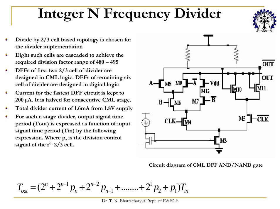
Integer N Frequency Divider
Circuit diagram of CML DFF AND/NAND gate
Divide by 2/3 cell based topology is chosen for the divider implementation
Eight such cells are cascaded to achieve the required division factor range of 480 – 495
DFFs of first two 2/3 cell of divider are designed in CML logic. DFFs of remaining six cell of divider are designed in digital logic
Current for the fastest DFF circuit is kept to 200 µA. It is halved for consecutive CML stage.
Total divider current of 1.6mA from 1.8V supply
For such n stage divider, output signal time period (Tout) is expressed as function of input signal time period (Tin) by the following expression. Where pr is the division control signal of the rth 2/3 cell.
1 2 11 2 1(2 2 2 ........ 2 )n n n
out n n inT p p p p T− −−= + + + + +
Dr. T. K. Bhattacharyya,Dept. of E&ECE
Integer N Frequency Divider
Simulated waveforms of divider for divide by 490
Dr. T. K. Bhattacharyya,Dept. of E&ECE
Layout of the chip
Die area: 1812.4um x 1965.04um

Dr. T. K. Bhattacharyya,Dept. of E&ECE
RF Transceiver Design:Power Amplifiers

Dr. T. K. Bhattacharyya,Dept. of E&ECE
PHASE NOISE AN ISSUE OF CONCERN
WHAT IS PHASE NOISE ?
It is the most critical parameter in the design of a high performance VCO or for that matter in any application requiring spectral purity
•When one talks about spectral purity he essentially means an impulse at the frequency of interest. But phase noise causes spilling around this central frequency of interest in the form of side bands.
•So instead of having all the energy concentrated at one single point in the frequency domain, the energy gets distributed at and around the central frequency leading to wastage of power
Dr. T. K. Bhattacharyya,Dept. of E&ECE
Phase noise manifests itself in the form of timing jitter (although there are other factorsthat contribute to jitter as we shall see shortly) in the time domain.Phase noise as the term suggests is addition of unwanted phase (phase angle) to any desired frequency. Mathematically, it is defined as a zero-mean stochastic process φ(t) in the general expression for the output voltage of an oscillator which is given by
Where the second term in the first bracket represents amplitude error while the time dependent phase term in the second bracket, φ(t) represents the phase error. In general the amplitude control mechanism takes care of the amplitude error and it is the phase error that is of real concern to us. (even if not taken care of completely the amplitude error is not of great concern to us. We are interested in the spectral purity of the signal.

Dr. T. K. Bhattacharyya,Dept. of E&ECE
What contributes to Phase noise ?
Any oscillator circuit consists of both passive as well as active components. They both contribute to noise. In general the noise is composed of the thermal noise, the flicker noise & the shot noise. Shot noise is a type of electronic noise that occurs when the finite number of particles that carry energy, such as electrons in an electronic circuit or photons in an optical device, is small enough to give rise to detectable statistical fluctuations in a measurement.

Dr. T. K. Bhattacharyya,Dept. of E&ECE
How To Deal With Phase Noise ?
Thus far we have dealt with phase noise in general but we will have to quantify it if we have to make it a basis of our design implementation and so the obvious question is how to interpret it or what kind of mathematical model do we have for it?As such there are three mathematical models (1) Linear Time Invariant model (2) Linear Time Variant model (3) Non-Linear Time Variant modelHere we will briefly present the important points of the first two models. The 3rd model although perfectly fine is way too complicated for us to make any use of it in practical implementation.The first model the linear time invariant one is due to Leeson and so is often referred to as Lesson's model. He derived an expression for the phase noise spectral density of a feedback oscillator. The general expression is

Dr. T. K. Bhattacharyya,Dept. of E&ECE
Where F is the circuit noise factor, k is the Boltzmann’s constant, T is the temperature,P0 is the oscillator output power, QL is the loaded quality factor of the resonator, ω0
is the oscillator fundamental frequency, ωC is the flicker noise corner frequency and Δω is the offset
frequency.
In fact Leeson’s model is a correction of an already existing model that ignored the noise contribution from the active devices. Actually if we take into account a lossless energy restoration device coupled with an LC tank
We would get the following equation

Dr. T. K. Bhattacharyya,Dept. of E&ECE
A comparison of the oscillator phase noise vs the offset frequency w.r.t. the central
frequency for the old model and the corrected model shows the effectiveness of Leeson’s model
But the fact that neither the corrected model nor the old one can make quantitative predictions about phase noise indicates that at least some of the assumptions used in the derivations are invalid, despite their apparent reasonableness. To develop a theory that does not possess the enumerated deficiencies we need to revisit, and perhaps revise these assumptions. And this was done by Lee and Hajimiri leading to the making of time variant model.
Dr. T. K. Bhattacharyya,Dept. of E&ECE
Lee and Hajimiri suggested that although the linear assumption is more or less valid, the time invariance would effectively mean that the irrespective of the point of time in the timedomain at which the noise or the error shows up it’s effect on the system would remain thesame. This assumption was challenged by them and they introduced something known as the impulse sensitivity factor Γ(x).
It gives us an idea of the disturbance an impulse of error would produce depending on the time at which it shows itself. Based on it the system could be so designed so as to ensure that the error which if unavoidable should be minimum.The ISF is a periodic function and has it’s maximum value at the zero crossings of a signal and minimum value (0) at the points where the signal (required) has it’s maximum value.
The figure on the shows the output of a LC oscillator and a ring oscillator in that order. While that on the bottom shows their impulse response in the same order.

Dr. T. K. Bhattacharyya,Dept. of E&ECE
A The impulsive phase disturbance can be written as
We can compute the excess phase using the superposition integral (In simple words simply sum up the contribution due to impulsive disturbances throughout the cycle)
A The ISF being a periodic function can be expressed as a Fourier series.
There isn’t exactly a healthy correlation between the various noise sources in the above expression and so the extra phase term in the cosine expression is ignored based on the assumption that the different noise sources are uncorrelated making their relative phase irrelevant.
Dr. T. K. Bhattacharyya,Dept. of E&ECE
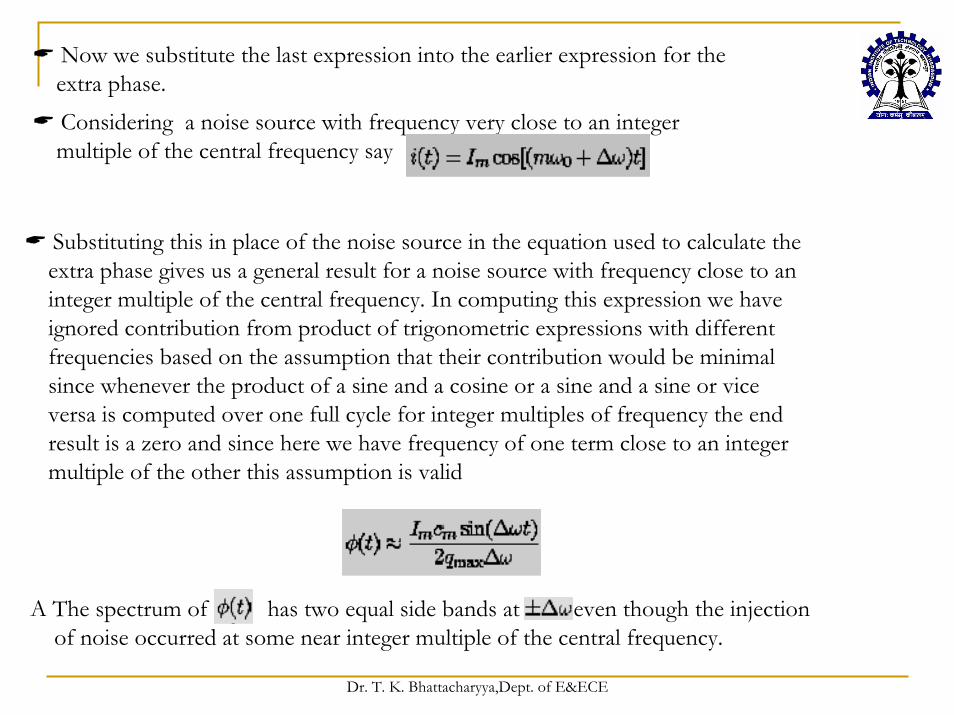
Now we substitute the last expression into the earlier expression for the extra phase.Considering a noise source with frequency very close to an integer multiple of the central frequency say
Substituting this in place of the noise source in the equation used to calculate the extra phase gives us a general result for a noise source with frequency close to an integer multiple of the central frequency. In computing this expression we have ignored contribution from product of trigonometric expressions with different frequencies based on the assumption that their contribution would be minimal since whenever the product of a sine and a cosine or a sine and a sine or vice versa is computed over one full cycle for integer multiples of frequency the end result is a zero and since here we have frequency of one term close to an integer multiple of the other this assumption is valid
A The spectrum of has two equal side bands at even though the injection of noise occurred at some near integer multiple of the central frequency.

Dr. T. K. Bhattacharyya,Dept. of E&ECE
The previous expressions simply give us an idea of excess phase but we need to see how it affects the output voltage. To do so we consider the general expression for the output voltage. Note that the amplitude noise or disturbance being mentioned here in this expression is already taken are of by the nonlinear amplitude control that exists in the oscillator.
Performing Phase to voltage conversion and assuming small amplitude disturbances, results in two equal power-sidebands symmetrically disposed about the central frequency
A Extending the above result to the general case of white noise gives us
It is clear from the above expression that minimizing the coefficients of ISF would ultimately minimize the phase noise. Another very apparent observation that can be made is that the power due to white noise sources varies as 1/ f2 thus explaining the middle segment of Leeson’s curve

Dr. T. K. Bhattacharyya,Dept. of E&ECE
The ISF approach is the more accurate approach amongst the existing methodologies. But the real problem with the ISF approach is the determination of the ISF function. Of the existing ways to determine the ISF the one that determines it most accurately is by carrying out transient analysis of the oscillator by feeding it with impulses varying in their timing from the start to the end of one cycle. The oscillator is simulated for a few cycles after the injection of the impulse. In order to use this method one has to have the oscillator design before hand.The simulation can be carried out in CADENCE software.
Once the ISF is known it needs to be expanded in a Fourier series to determine the Fourier coefficients. One may also use Fourier analysis directly ( in order to determine the various coefficients ) if we have the complete ISF curve (MATLAB can be used for this purpose).
Apart from it we would be needing the device noise 1/f corner frequency and a specification of the offset from the central frequency at which we wish to calculate the phase noise
Phase Noise Prediction

Dr. T. K. Bhattacharyya,Dept. of E&ECE
TRADE OFFS•supply voltage•output power,•power efficiency•distortion
REQUIREMENTS•Ability to work at low supply voltages •High operating frequencies.
Dr. T. K. Bhattacharyya,Dept. of E&ECE

Dr. T. K. Bhattacharyya,Dept. of E&ECE
CMOS PA: Related Design Issues
Low breakdown voltage of deep sub-micron technologies Substrate interaction in a highly integrated CMOS IC Low value of optimum load resistance requires higher impedance transformation ratioLow Q values of inductors PA delivers large output current – parasitics in circuit may cause performance degradationConventional transistor models for CMOS devices are moderately inaccurate for RFICs.
Dr. T. K. Bhattacharyya,Dept. of E&ECE
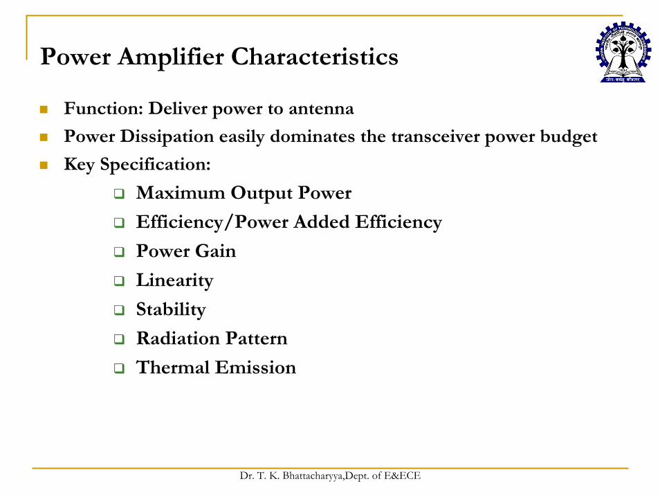
Power Amplifier Characteristics
Function: Deliver power to antenna
Power Dissipation easily dominates the transceiver power budget
Key Specification:
Maximum Output Power
Efficiency/Power Added Efficiency
Power Gain
Linearity
Stability
Radiation Pattern
Thermal Emission
Dr. T. K. Bhattacharyya,Dept. of E&ECE
PERFORMANCE METRICS
Output PowerEfficiencyLinearity

Dr. T. K. Bhattacharyya,Dept. of E&ECE
Output PowerPower delivered to the load within the band of interest.
Load is usually an antenna with Z0 of 50Ω
Doesn’t include power contributed by the harmonics or any unwanted spurs
Sinusoidal
Modulated Signal
Dr. T. K. Bhattacharyya,Dept. of E&ECE
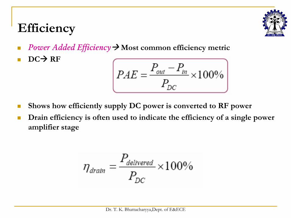
EfficiencyPower Added Efficiency Most common efficiency metric
DC RF
Shows how efficiently supply DC power is converted to RF power
Drain efficiency is often used to indicate the efficiency of a single power amplifier stage
Dr. T. K. Bhattacharyya,Dept. of E&ECE
Linearity
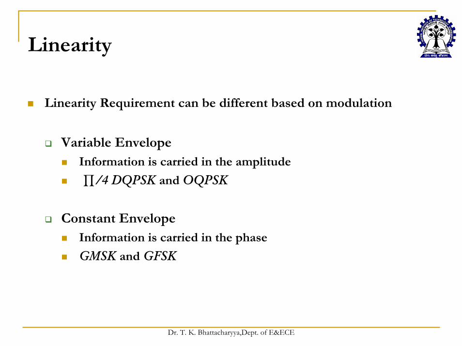
Linearity Requirement can be different based on modulation
Variable EnvelopeInformation is carried in the amplitude
∏/4 DQPSK and OQPSK
Constant EnvelopeInformation is carried in the phase
GMSK and GFSK
Dr. T. K. Bhattacharyya,Dept. of E&ECE
CLASSIFICATION OF RF POWER AMPLIFIER
LinearSwitch mode

Dr. T. K. Bhattacharyya,Dept. of E&ECE
Linear PA: Class A,B,AB and C
transistor acts as a current source
Since certain amount of voltage must exist to keep the device in the current source mode, there is always certain power dissipation on the device
Switch mode PA: Class D,E,F
Active device acts as a switch
There is either zero voltage across or zero current through a switch
100% efficiency possible

Dr. T. K. Bhattacharyya,Dept. of E&ECE
Resistor Loaded Class A Amplifier
In a Class A amplifier, the active device conducts current 100% of time
For maximum output swing (and thus output power), the quiescent output voltage is set at VDD/2, and bias current at VDD/2RL
Dr. T. K. Bhattacharyya,Dept. of E&ECE
Other Power Efficiency Parameters
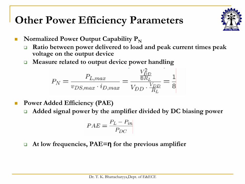
Normalized Power Output Capability PN
Ratio between power delivered to load and peak current times peak voltage on the output deviceMeasure related to output device power handling
Power Added Efficiency (PAE)Added signal power by the amplifier divided by DC biasing power
At low frequencies, PAE=η for the previous amplifier
Dr. T. K. Bhattacharyya,Dept. of E&ECE
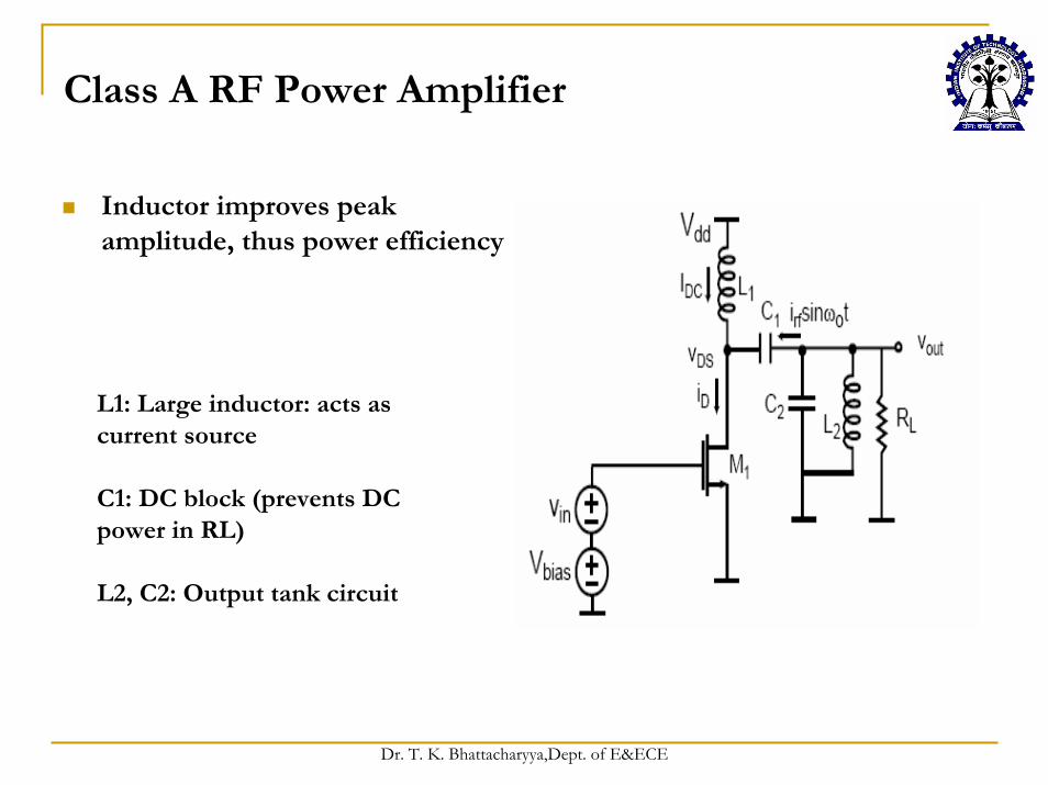
Class A RF Power Amplifier
Inductor improves peak amplitude, thus power efficiency
L1: Large inductor: acts as current source
C1: DC block (prevents DC power in RL)
L2, C2: Output tank circuit
Dr. T. K. Bhattacharyya,Dept. of E&ECE
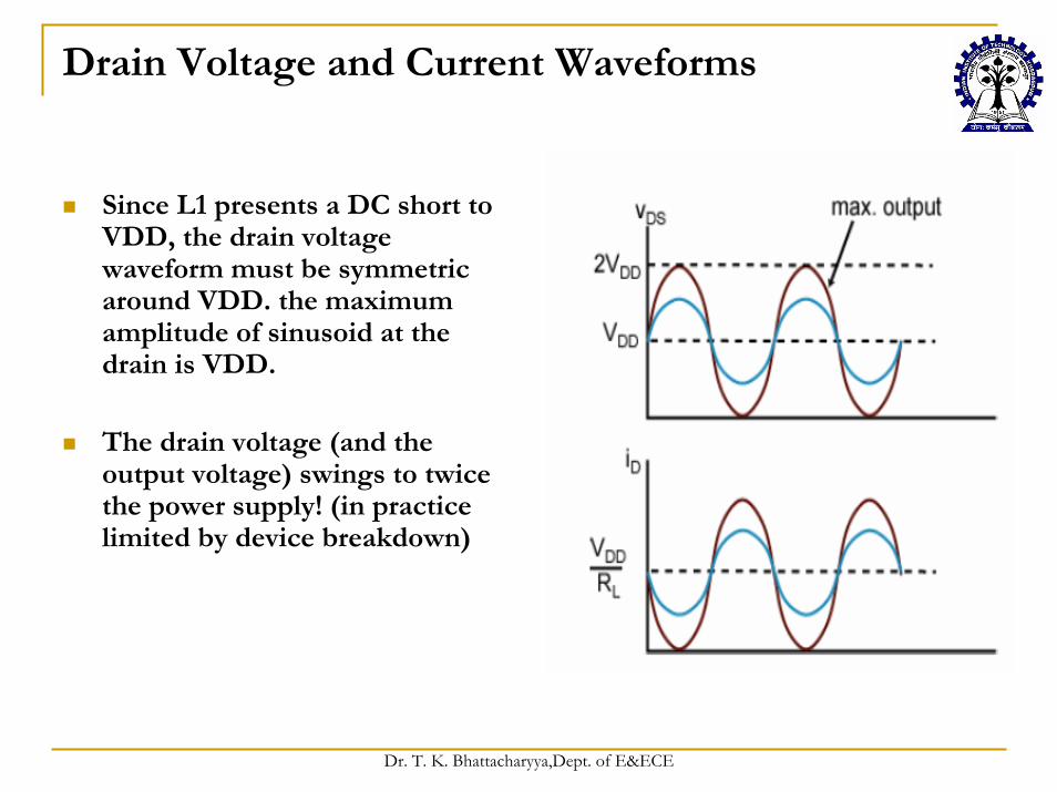
Drain Voltage and Current Waveforms
Since L1 presents a DC short to VDD, the drain voltage waveform must be symmetric around VDD. the maximum amplitude of sinusoid at the drain is VDD.
The drain voltage (and the output voltage) swings to twice the power supply! (in practice limited by device breakdown)

Dr. T. K. Bhattacharyya,Dept. of E&ECE
Normalized Power Output Capability
Class A amplifiers are linear, but have poor efficiency!

Dr. T. K. Bhattacharyya,Dept. of E&ECE
Class B Power Amplifier
Same circuit, but Vbias is set so that M1 conducts only 50% of time

Dr. T. K. Bhattacharyya,Dept. of E&ECE
Class B Power Amplifier
Vbias is set so that M1 conducts only 50% of time
The harmonics in the output waveform are filtered by output tank circuit
The fundamental component is a linear function of the input
Dr. T. K. Bhattacharyya,Dept. of E&ECE
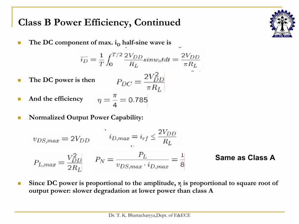
Class B Power Efficiency, Continued
The DC component of max. iD half-sine wave is
The DC power is then
And the efficiency
Normalized Output Power Capability:
Since DC power is proportional to the amplitude, η is proportional to square root of output power: slower degradation at lower power than class A
Same as Class A

Dr. T. K. Bhattacharyya,Dept. of E&ECE
Conduction Angle vs. Class
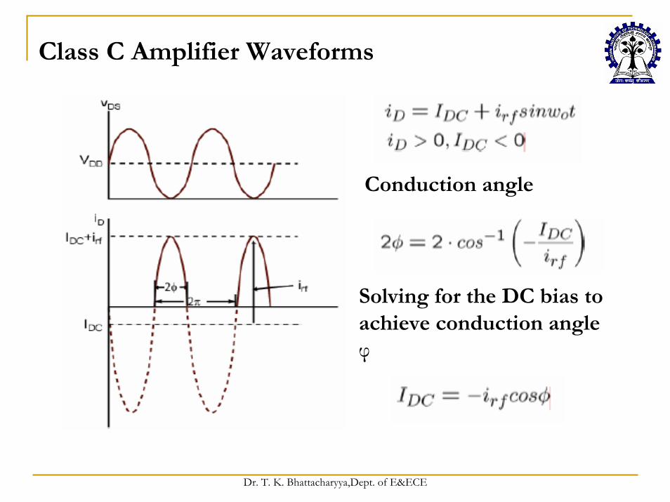
Conduction Angle φ :2φ is the portion of period during which the output transistor M1 conducts
2φ=2π: Class Aπ<2φ<2π: Class AB2φ=π: Class B0<2φ<π: Class C
(Class AB or C output cannot be a linear function of input)

Dr. T. K. Bhattacharyya,Dept. of E&ECE
Push-Pull Amplifier
Depending on Vbias and Vinpush- pull amplifier can be operated as Class A, B, AB, C, or D amplifier.Theoretically a Class B push- pull amplifier has low distortion comparable to class A because either half will be conducting at any time.Real Class B is not possible because devices do not have abrupt turn- on characteristic–most are Class AB

Dr. T. K. Bhattacharyya,Dept. of E&ECE
Voltage and Current Waveforms of Class B Push-Pull
Waveforms shown for maximum amplitude output
typically, ‘crossover distortion’ arises at the switching point of the two halves due to imprecise turn-on voltages
Crossover distortion is reduced by class AB operation

Dr. T. K. Bhattacharyya,Dept. of E&ECE
Class C Amplifier
Same amplifier, but biased to conduct less than 50% of time
The output amplitude is not a linear function of input: more suitable for constant-amplitude power amp (such as in PM or FM)
Dr. T. K. Bhattacharyya,Dept. of E&ECE
Class C Amplifier Waveforms
Conduction angle
Solving for the DC bias to achieve conduction angle φ

Dr. T. K. Bhattacharyya,Dept. of E&ECE
Class C Power Efficiency Calculation
The average value of iD
The fundamental component of iD
Maximum output swing is reached when

Dr. T. K. Bhattacharyya,Dept. of E&ECE
Class C Power Efficiency, Continued
Maximum efficiency is then
The normalized output capability is poor at small conduction angles
Thus, the efficiency must be sacrificed for reasonable PN
Dr. T. K. Bhattacharyya,Dept. of E&ECE
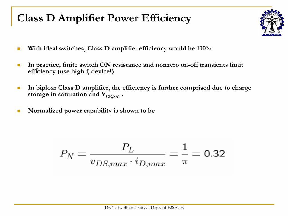
Class D Amplifier Power Efficiency
With ideal switches, Class D amplifier efficiency would be 100%
In practice, finite switch ON resistance and nonzero on-off transients limit efficiency (use high ft device!)
In biploar Class D amplifier, the efficiency is further comprised due to charge storage in saturation and VCE,SAT.
Normalized power capability is shown to be
Dr. T. K. Bhattacharyya,Dept. of E&ECE
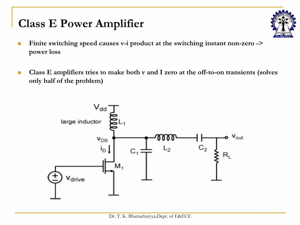
Class E Power Amplifier
Finite switching speed causes v-i product at the switching instant non-zero -> power loss
Class E amplifiers tries to make both v and I zero at the off-to-on transients (solves only half of the problem)

Dr. T. K. Bhattacharyya,Dept. of E&ECE
Typical Voltage and Current Waveforms
Source: Shawn Kuo,’Linearization of a PulseWidth Modulated Power Amplifier,” S.B. Thesis, MIT, June 2004
Dr. T. K. Bhattacharyya,Dept. of E&ECE
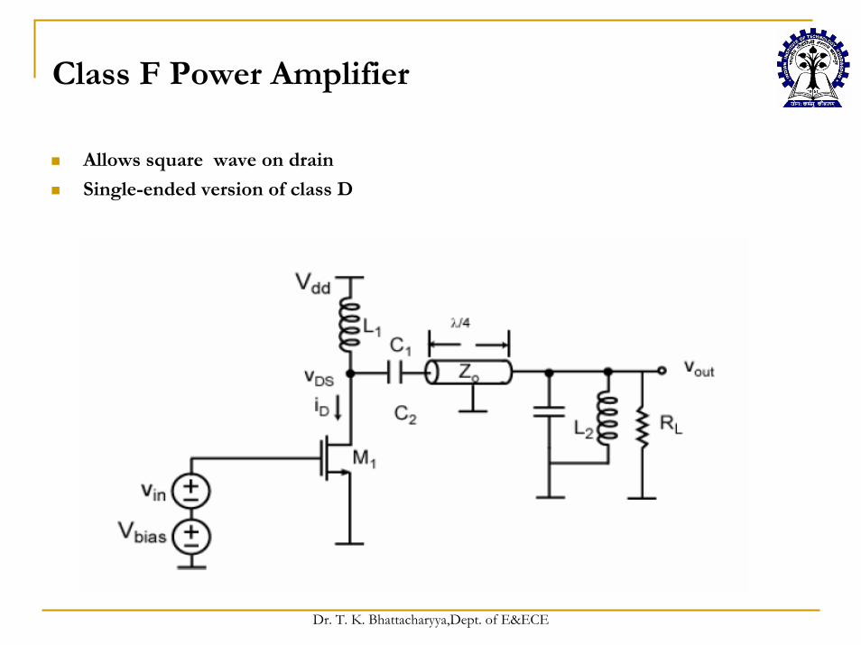
Class F Power Amplifier
Allows square wave on drain
Single-ended version of class D

Dr. T. K. Bhattacharyya,Dept. of E&ECE
Class F Power Amplifier Waveforms
The waveforms are similar to half of class D Push-Pull

Dr. T. K. Bhattacharyya,Dept. of E&ECE
Class F Power Amplifier Analysis
Refer Thomas. H. Lee’s book
Amplitude of fundamental frequency of drain voltage
Power delivered to the load

Dr. T. K. Bhattacharyya,Dept. of E&ECE
Linearization Techniques
How to linearize highly efficient PAs?

Dr. T. K. Bhattacharyya,Dept. of E&ECE
Linearization Techniques
Non-linear power amplifier can reach great efficienciesBut they lack linearityLinearization techniques can be applied to non-linear PAs to get a good linearity and a modest efficiencyControl is applied at
InputBack-offPre-distortionCartesian feedbackPolar feedback
OutputFeed-forwardLINC (Linearization using Nonlinear Components)
Supply EER (Envelope Elimination and Restoration)

Dr. T. K. Bhattacharyya,Dept. of E&ECE
Input: Back-off
Simplest and most common linearization
PAE is greatly reduced

Dr. T. K. Bhattacharyya,Dept. of E&ECE
Input: Pre-distortion
Tracking gain and change variations of amplifier is very challenging using analog techniquesDigital Look-up tables often usedPA gain and phase response varies with bias,
temperature and supply changes
Dr. T. K. Bhattacharyya,Dept. of E&ECE
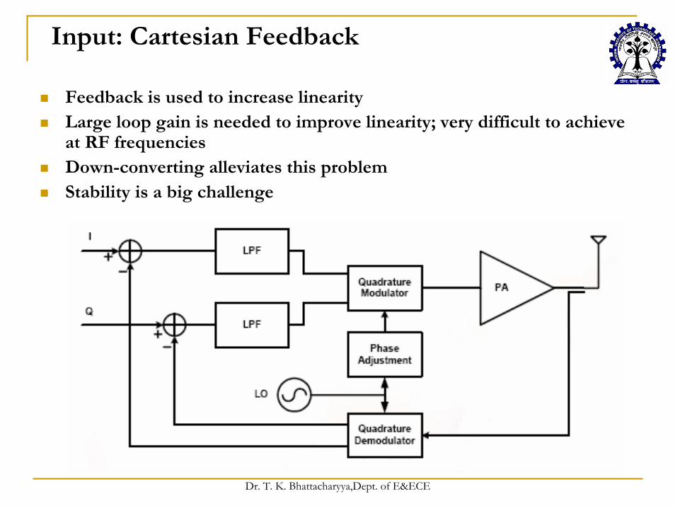
Input: Cartesian Feedback
Feedback is used to increase linearityLarge loop gain is needed to improve linearity; very difficult to achieve at RF frequenciesDown-converting alleviates this problemStability is a big challenge
Dr. T. K. Bhattacharyya,Dept. of E&ECE
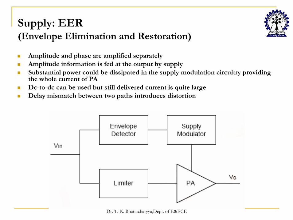
Supply: EER(Envelope Elimination and Restoration)
Amplitude and phase are amplified separatelyAmplitude information is fed at the output by supplySubstantial power could be dissipated in the supply modulation circuitry providing the whole current of PADc-to-dc can be used but still delivered current is quite largeDelay mismatch between two paths introduces distortion