mos ak noise in rf circuits and rf noise device ... · noise in rf circuits and rf noise device...
TRANSCRIPT
MOS AK
Noise in RF Circuits and RF Noise DeviceCharacterizationDate 20.4.2007
Peter Baumgartner
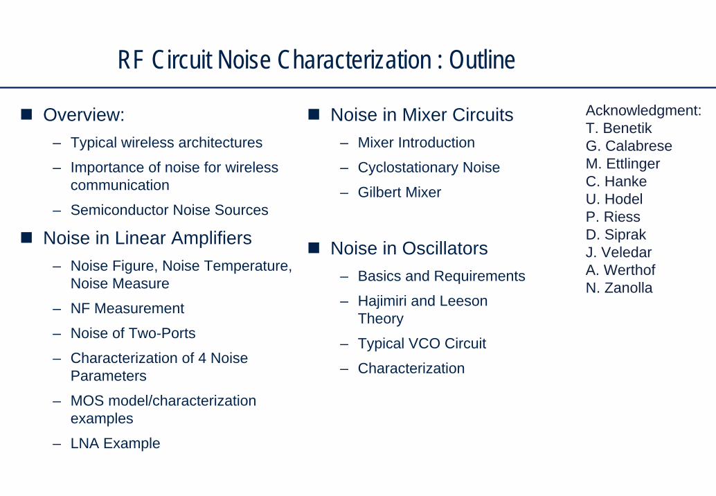
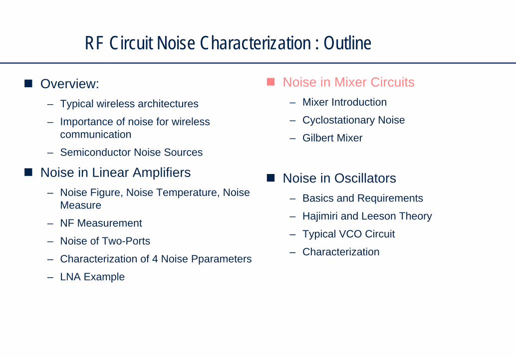
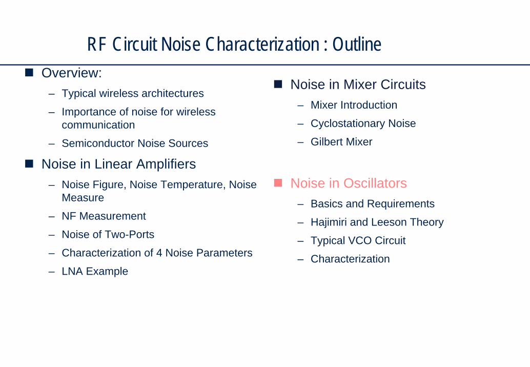
RF Circuit Noise Characterization : Outline
Overview:– Typical wireless architectures
– Importance of noise for wireless communication
– Semiconductor Noise Sources
Noise in Linear Amplifiers– Noise Figure, Noise Temperature,
Noise Measure
– NF Measurement
– Noise of Two-Ports
– Characterization of 4 Noise Parameters
– MOS model/characterization examples
– LNA Example
Noise in Mixer Circuits– Mixer Introduction
– Cyclostationary Noise
– Gilbert Mixer
Noise in Oscillators– Basics and Requirements
– Hajimiri and LeesonTheory
– Typical VCO Circuit
– Characterization
Acknowledgment:T. BenetikG. CalabreseM. EttlingerC. HankeU. HodelP. RiessD. SiprakJ. VeledarA. WerthofN. Zanolla
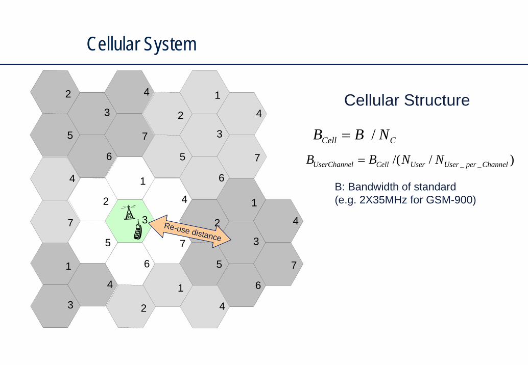
Cellular System
1
2
3
4
5
6
7
1
2
3
4
5
6
7
1
2
3
4
5
6
7
1
2 4
1
3
4
4
7
2
3
4
5
6
7 CCell NBB /=
Re-use distance
)//( __ ChannelperUserUserCelllUserChanne NNBB
Cellular Structure
=
B: Bandwidth of standard(e.g. 2X35MHz for GSM-900)
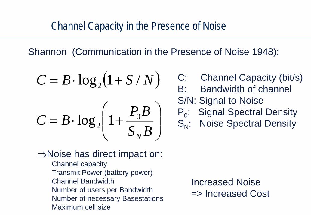
Channel Capacity in the Presence of Noise
⎟⎟⎠
⎞⎜⎜⎝
⎛+⋅=
BSBPBC
N
02 1log
Shannon (Communication in the Presence of Noise 1948):
( )NSBC /1log2 +⋅= C: Channel Capacity (bit/s)B: Bandwidth of channelS/N: Signal to NoiseP0: Signal Spectral DensitySN: Noise Spectral Density
⇒Noise has direct impact on:Channel capacityTransmit Power (battery power)Channel BandwidthNumber of users per BandwidthNumber of necessary BasestationsMaximum cell size
Increased Noise=> Increased Cost
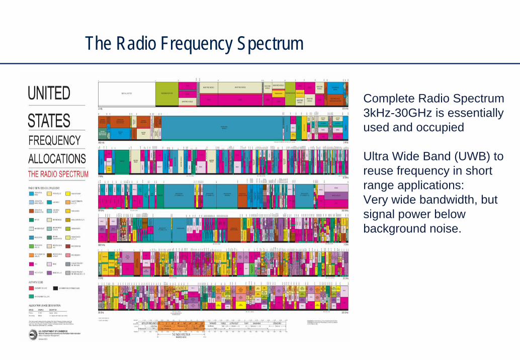
The Radio Frequency Spectrum
Complete Radio Spectrum3kHz-30GHz is essentially used and occupied
Ultra Wide Band (UWB) to reuse frequency in short range applications:Very wide bandwidth, but signal power below background noise.
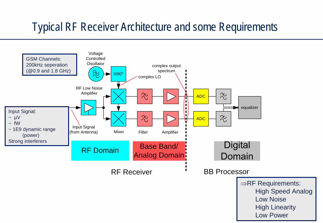
Typical RF Receiver Architecture and some Requirements
ADC
equalizer
ADC
0/90°complex LO
Input Signal(from Antenna)
complex outputspectrum
RF Low NoiseAmplifier
VoltageControlledOscillator
Mixer Filter Amplifier
RF Domain Base Band/Analog Domain
RF Receiver BB Processor
Input Signal:~ µV~ fW~ 1E9 dynamic range
(power)Strong interferers
GSM Channels:200kHz seperation(@0.9 and 1.8 GHz)
⇒RF Requirements:High Speed AnalogLow NoiseHigh LinearityLow Power
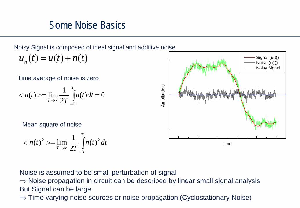
Some Noise Basics
)()()( tntutun +=
∫−
∞→>=<
T
TT
dttnT
tn 22 )(21lim)(
∫−
∞→=>=<
T
TT
dttnT
tn 0)(21lim)(
Ampl
itude
u
time
Signal (u(t)) Noise (n(t)) Noisy Signal
Noisy Signal is composed of ideal signal and additive noise
Time average of noise is zero
Mean square of noise
Noise is assumed to be small perturbation of signal⇒ Noise propagation in circuit can be described by linear small signal analysisBut Signal can be large⇒ Time varying noise sources or noise propagation (Cyclostationary Noise)
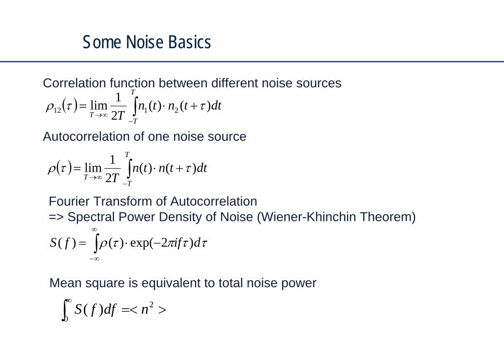
Some Noise Basics
( ) ∫−
∞→+⋅=
T
TT
dttntnT
)()(21lim 2112 ττρ
( ) ∫−
∞→+⋅=
T
TT
dttntnT
)()(21lim ττρ
∫∞
∞−
−⋅= ττπτρ diffS )2exp()()(
Fourier Transform of Autocorrelation => Spectral Power Density of Noise (Wiener-Khinchin Theorem)
∫∞
>=<0
2)( ndffS
Correlation function between different noise sources
Autocorrelation of one noise source
Mean square is equivalent to total noise power
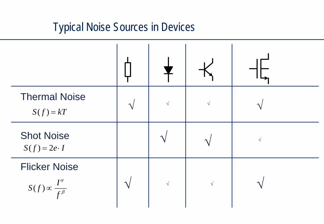
Typical Noise Sources in Devices
Thermal Noise
Shot Noise
Flicker Noise
√ √
√
√ √
√ √
√√
√
kTfS =)(
IefS ⋅= 2)(
β
α
fIfS ∝)(
√
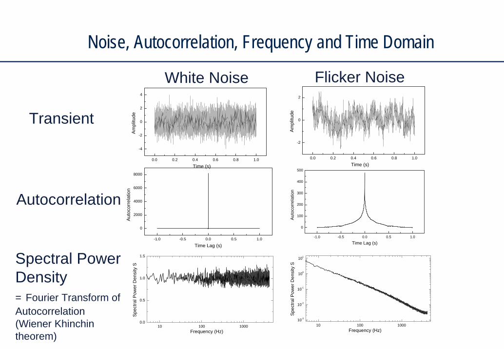
Noise, Autocorrelation, Frequency and Time Domain
0.0 0.2 0.4 0.6 0.8 1.0
-4
-2
0
2
4
Am
plitu
de
Time (s)
10 100 10000.0
0.5
1.0
1.5
Frequency (Hz)
Spe
ctra
l Pow
er D
ensi
ty S
-1.0 -0.5 0.0 0.5 1.0
0
2000
4000
6000
8000
Aut
ocor
rela
tion
Time Lag (s)
0.0 0.2 0.4 0.6 0.8 1.0
-2
0
2
Ampl
itude
Time (s)
-1.0 -0.5 0.0 0.5 1.0
0
100
200
300
400
500
Aut
ocor
rela
tion
Time Lag (s)
10 100 100010-3
10-2
10-1
100
101
Frequency (Hz)
Spe
ctra
l Pow
er D
ensi
ty S
White Noise Flicker Noise
Transient
Autocorrelation
Spectral Power Density= Fourier Transform of Autocorrelation (Wiener Khinchintheorem)
RF Circuit Noise Characterization : Outline
Overview:– Typical wireless architectures
– Importance of noise for wireless communication
– Semiconductor Noise Sources
Noise in Linear Amplifiers– Noise Figure, Noise Temperature, Noise
Measure
– NF Measurement
– Noise of Two-Ports
– Characterization of 4 Noise Pparameters
– LNA Example
Noise in Mixer Circuits– Mixer Introduction
– Cyclostationary Noise
– Gilbert Mixer
Noise in Oscillators– Basics and Requirements
– Hajimiri and Leeson Theory
– Typical VCO Circuit
– Characterization
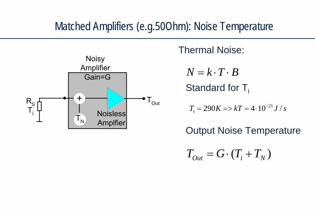
Matched Amplifiers (e.g.50Ohm): Noise Temperature
BTkN ⋅⋅=
sJkTKTi /104290 21−⋅==>=
)( NiOut TTGT +⋅=
Thermal Noise:
Standard for Ti
Output Noise TemperatureN
S
i
Out
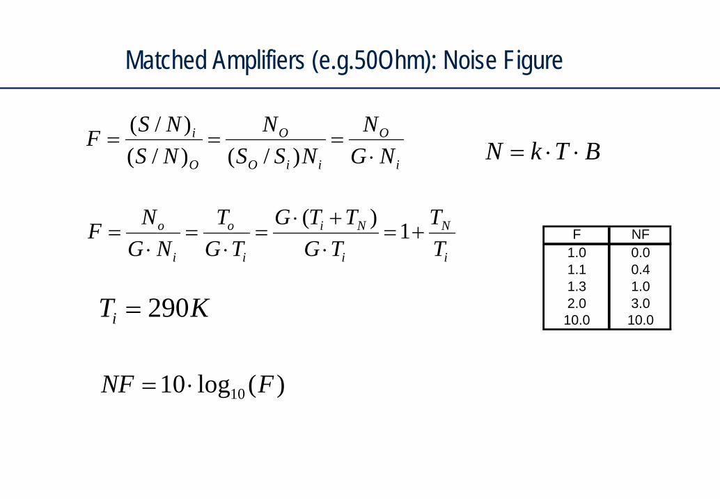
Matched Amplifiers (e.g.50Ohm): Noise Figure
i
O
iiO
O
O
i
NGN
NSSN
NSNSF
⋅===
)/()/()/(
)(log10 10 FNF ⋅=
KTi 290=
F NF1.0 0.01.1 0.41.3 1.02.0 3.010.0 10.0
BTkN ⋅⋅=
i
N
i
Ni
i
o
i
o
TT
TGTTG
TGT
NGNF +=
⋅+⋅
=⋅
=⋅
= 1)(
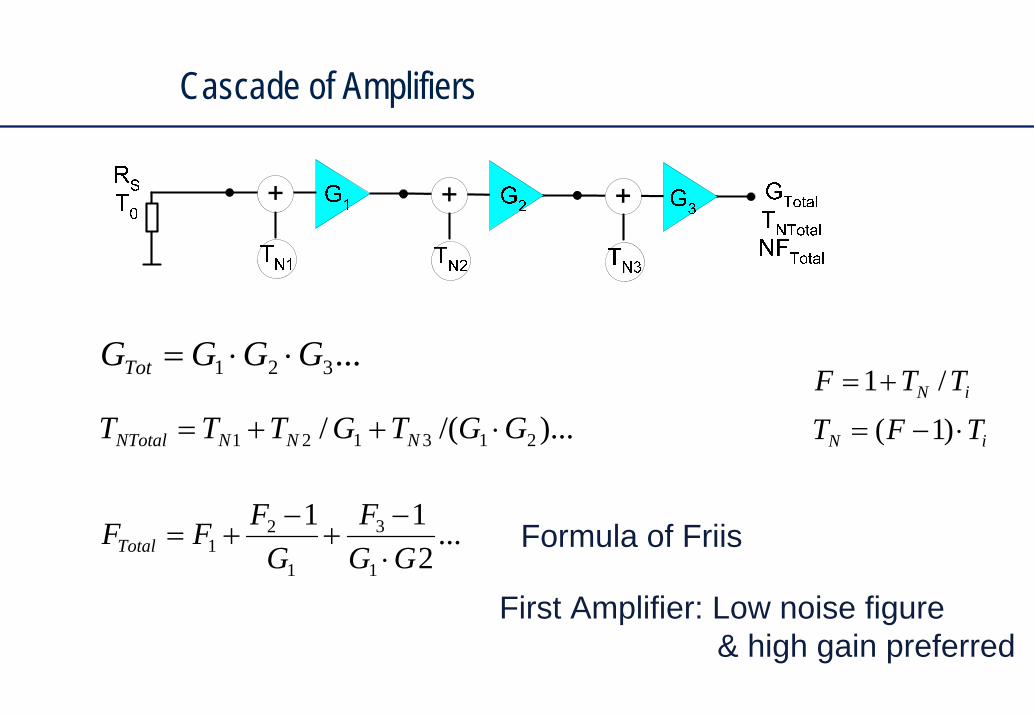
Cascade of Amplifiers
...321 GGGGTot ⋅⋅=
).../(/ 213121 GGTGTTT NNNNTotal ⋅++=
...211
1
3
1
21 GG
FG
FFFTotal ⋅−
+−
+=
iN TTF /1+=
iN TFT ⋅−= )1(
Formula of Friis
First Amplifier: Low noise figure& high gain preferred
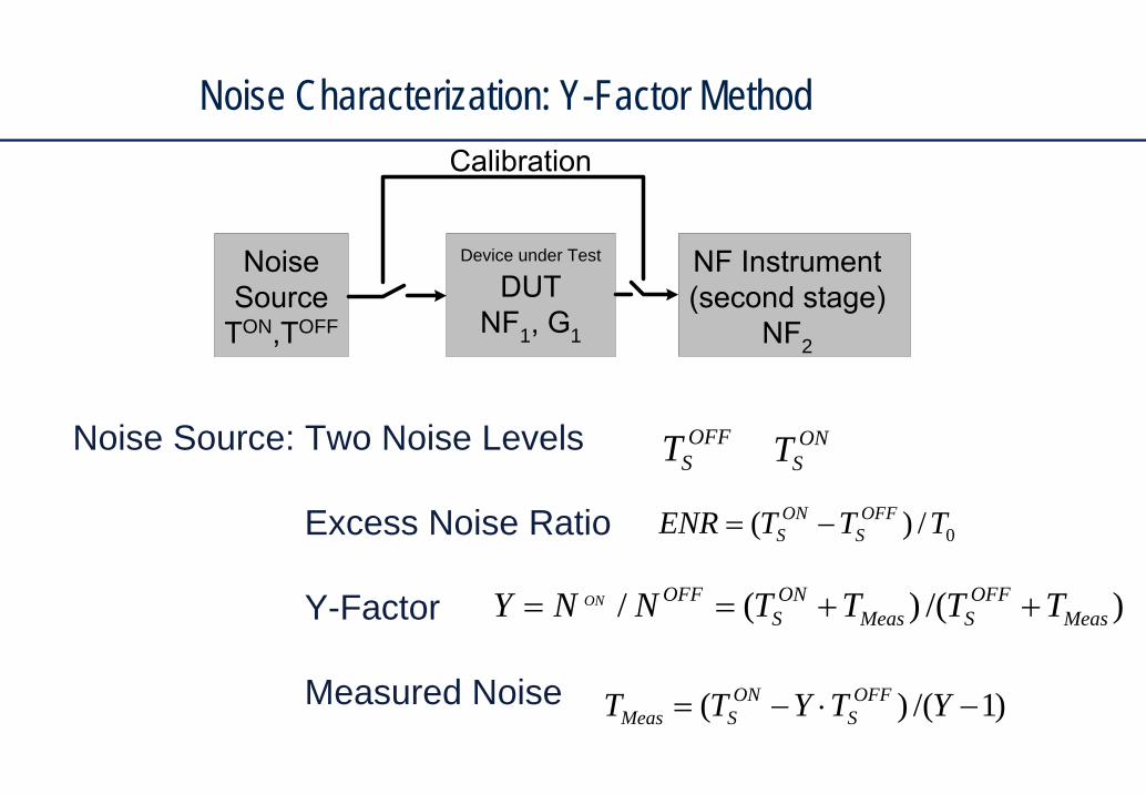
Noise Characterization: Y-Factor Method
)/()(/ MeasOFF
SMeasON
SOFF TTTTNNY ON ++==
ONSTOFF
STNoise Source: Two Noise Levels
Excess Noise Ratio
Y-Factor
Measured Noise
0/)( TTTENR OFFS
ONS −=
ON OFF
Device under Test
1 1 2
)1/()( −⋅−= YTYTT OFFS
ONSMeas
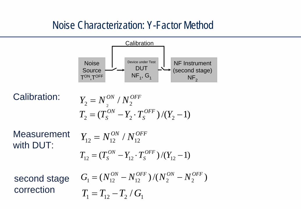
Noise Characterization: Y-Factor Method
OFFON NNY 22 /2
=)1/()( 222 −⋅−= YTYTT OFF
SON
S
)1/()( 121212 −⋅−= YTYTT OFFS
ONS
NoiseSource
TON,TOFF
Device under Test
DUTNF1, G1
NF Instrument(second stage)
NF2
Calibration
Calibration:
Measurementwith DUT:
OFFON NNY 121212 /=
second stagecorrection
)/()( 2212121OFFONOFFON NNNNG −−=
12121 / GTTT −=
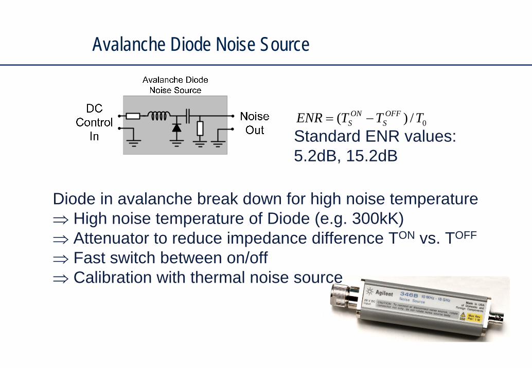
Avalanche Diode Noise Source
0/)( TTTENR OFFS
ONS −=
Diode in avalanche break down for high noise temperature⇒ High noise temperature of Diode (e.g. 300kK)⇒ Attenuator to reduce impedance difference TON vs. TOFF
⇒ Fast switch between on/off⇒ Calibration with thermal noise source
Standard ENR values:5.2dB, 15.2dB
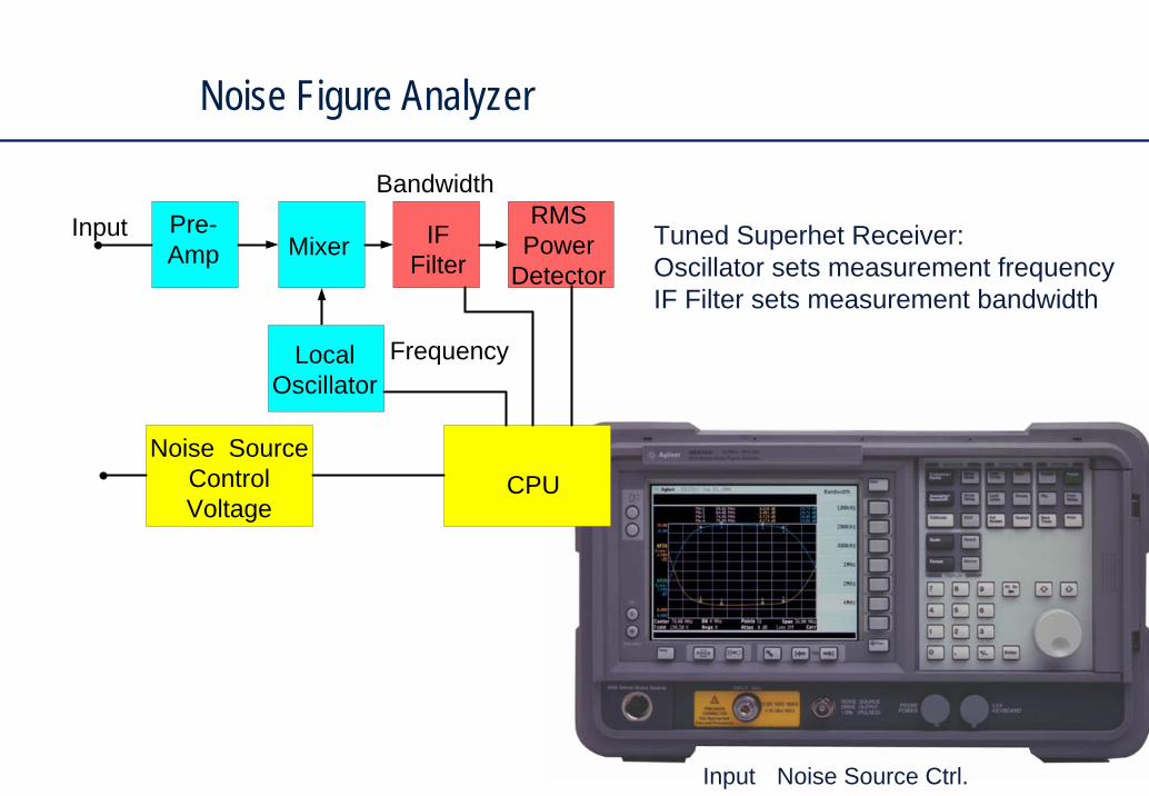
Noise Figure Analyzer
Tuned Superhet Receiver:Oscillator sets measurement frequencyIF Filter sets measurement bandwidth
Pre-Amp Mixer IF
Filter
RMSPower
Detector
LocalOscillator
Frequency
Bandwidth
Input
Noise SourceControlVoltage
CPU
Input Noise Source Ctrl.
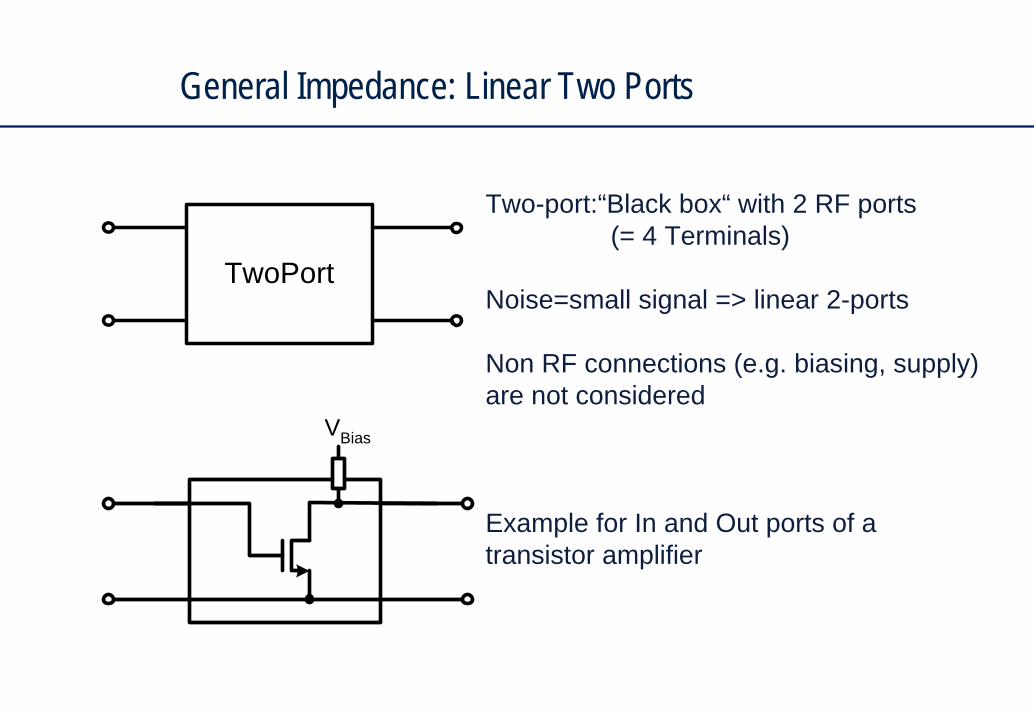
General Impedance: Linear Two Ports
TwoPort
VBias
Two-port:“Black box“ with 2 RF ports (= 4 Terminals)
Noise=small signal => linear 2-ports
Non RF connections (e.g. biasing, supply)are not considered
Example for In and Out ports of a transistor amplifier
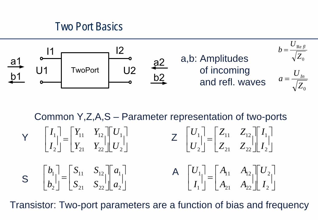
Two Port Basics
0ZUa In=
0
Re
ZU
b fl=a,b: Amplitudes
of incomingand refl. waves
Y Z
Common Y,Z,A,S – Parameter representation of two-ports
S
⎥⎦
⎤⎢⎣
⎡⎥⎦
⎤⎢⎣
⎡=⎥
⎦
⎤⎢⎣
⎡
2
1
2221
1211
2
1
UU
YYYY
II
⎥⎦
⎤⎢⎣
⎡⎥⎦
⎤⎢⎣
⎡=⎥
⎦
⎤⎢⎣
⎡
2
1
2221
1211
2
1
II
ZZZZ
UU
⎥⎦
⎤⎢⎣
⎡⎥⎦
⎤⎢⎣
⎡=⎥
⎦
⎤⎢⎣
⎡
2
1
2221
1211
2
1
aa
SSSS
bb
⎥⎦
⎤⎢⎣
⎡⎥⎦
⎤⎢⎣
⎡=⎥
⎦
⎤⎢⎣
⎡
2
2
2221
1211
1
1
IU
AAAA
IUA
Transistor: Two-port parameters are a function of bias and frequency
Two Port Basics
⎥⎦
⎤⎢⎣
⎡⎥⎦
⎤⎢⎣
⎡=⎥
⎦
⎤⎢⎣
⎡
2
2
2221
1211
1
1
IU
AAAA
IU
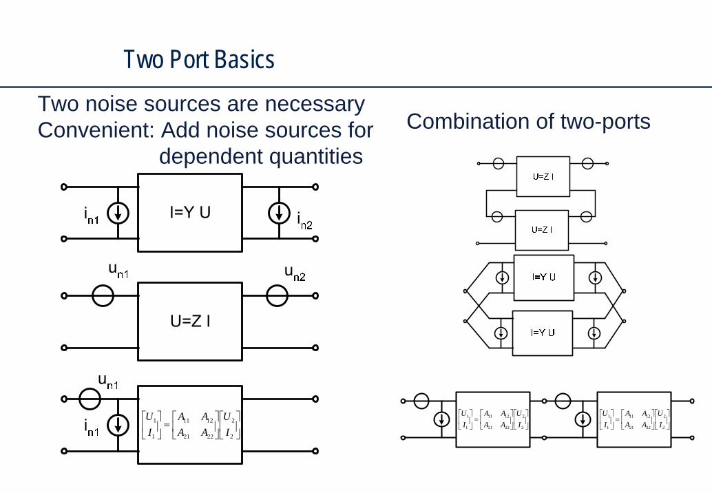
Two noise sources are necessaryConvenient: Add noise sources for
dependent quantitiesCombination of two-ports
⎥⎦
⎤⎢⎣
⎡⎥⎦
⎤⎢⎣
⎡=⎥
⎦
⎤⎢⎣
⎡
2
2
2221
1211
1
1
IU
AAAA
IU
⎥⎦
⎤⎢⎣
⎡⎥⎦
⎤⎢⎣
⎡=⎥
⎦
⎤⎢⎣
⎡
2
2
2221
1211
1
1
IU
AAAA
IU
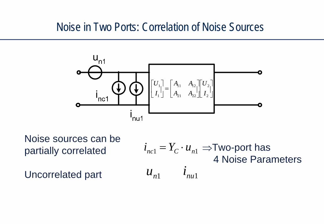
Noise in Two Ports: Correlation of Noise Sources
⎥⎦
⎤⎢⎣
⎡⎥⎦
⎤⎢⎣
⎡=⎥
⎦
⎤⎢⎣
⎡
2
2
2221
1211
1
1
IU
AAAA
IU
11 nCnc uYi ⋅=
1nui1nu
⇒Two-port has4 Noise Parameters
Noise sources can be partially correlated
Uncorrelated part
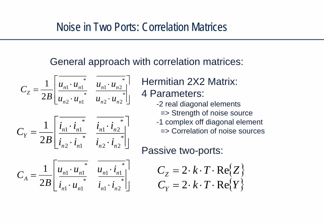
Noise in Two Ports: Correlation Matrices
⎥⎥⎦
⎤
⎢⎢⎣
⎡
⋅⋅
⋅⋅=*
22*
12
*21
*11
21
nnnn
nnnnY
iiiiiiii
BC
General approach with correlation matrices:
⎥⎥⎦
⎤
⎢⎢⎣
⎡
⋅⋅
⋅⋅=*
22*
12
*21
*11
21
nnnn
nnnnZ
uuuuuuuu
BC
⎥⎥⎦
⎤
⎢⎢⎣
⎡
⋅⋅
⋅⋅=*
21*
11
*11
*11
21
nnnn
nnnnA
iiuiiuuu
BC
Hermitian 2X2 Matrix:4 Parameters:
-2 real diagonal elements => Strength of noise source
-1 complex off diagonal element=> Correlation of noise sources
Passive two-ports:
{ }ZTkCZ Re2 ⋅⋅⋅={ }YTkCY Re2 ⋅⋅⋅=
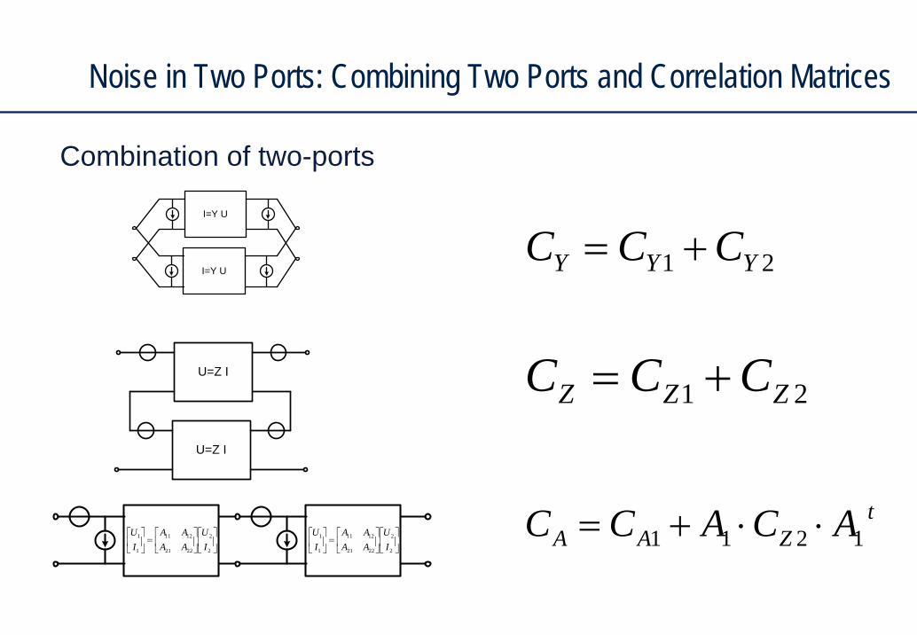
Noise in Two Ports: Combining Two Ports and Correlation Matrices
U=Z I
U=Z I
21 YYY CCC +=
Combination of two-ports
I=Y U
I=Y U
⎥⎦
⎤⎢⎣
⎡⎥⎦
⎤⎢⎣
⎡=⎥
⎦
⎤⎢⎣
⎡
2
2
2221
1211
1
1
IU
AAAA
IU
⎥⎦
⎤⎢⎣
⎡⎥⎦
⎤⎢⎣
⎡=⎥
⎦
⎤⎢⎣
⎡
2
2
2221
1211
1
1
IU
AAAA
IU
21 ZZZ CCC +=
tZAA ACACC 1211 ⋅⋅+=
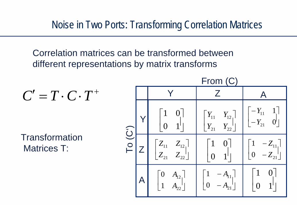
Noise in Two Ports: Transforming Correlation Matrices
+⋅⋅=′ TCTC
⎥⎦
⎤⎢⎣
⎡1001
Correlation matrices can be transformed between different representations by matrix transforms
⎥⎦
⎤⎢⎣
⎡
2221
1211
YYYY ⎥
⎦
⎤⎢⎣
⎡−−
01
21
11
YY
⎥⎦
⎤⎢⎣
⎡
2221
1211
ZZZZ
⎥⎦
⎤⎢⎣
⎡
22
12
10
AA
⎥⎦
⎤⎢⎣
⎡−−
21
11
01
AA
⎥⎦
⎤⎢⎣
⎡−−
21
11
01
ZZ
⎥⎦
⎤⎢⎣
⎡1001
⎥⎦
⎤⎢⎣
⎡1001
TransformationMatrices T:
Y Z A
Y
Z
A
From (C)
To (C
‘)
Noise Deembedding with Correlation Matrices
YS ⇒
G
G G
G
S S
Por
t 1
Por
t 2
Device Teststructure
S-Param.C Noiseparam.
Open Deemb.
S-Param.
Dee
mbe
ddin
gS
teps
YCC ⇒OpenOpen YS ⇒{ }OpenOpenY YkTC Re2 ⋅=−
OpenDeemb YYY −=
OpenYYDeembY CCC −− −=
Mea
sure
men
t
I=Y U
I=Y U
Device
Pad-Cap.
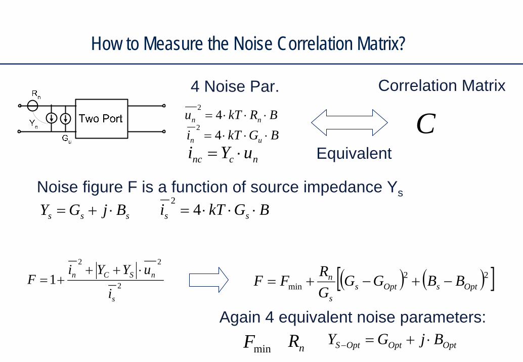
How to Measure the Noise Correlation Matrix?
BRkTu nn ⋅⋅⋅= 42
BGkTi un ⋅⋅⋅= 42
ncnc uYi ⋅=
4 Noise Par. Correlation Matrix
EquivalentC
Noise figure F is a function of source impedance Ys
BGkTi ss ⋅⋅⋅= 42
2
22
1s
nSCn
i
uYYiF
⋅+++=
sss BjGY ⋅+=
( ) ( )[ ]22min OptsOpts
s
n BBGGGRFF −+−+=
Again 4 equivalent noise parameters:
minF nR OptOptOptS BjGY ⋅+=−
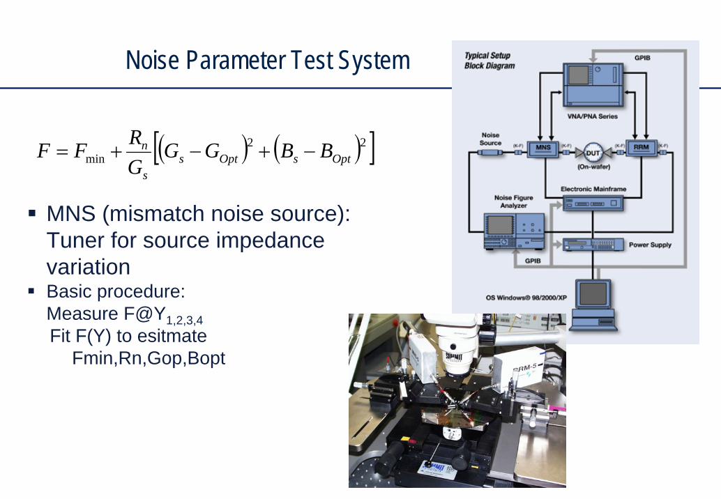
Noise Parameter Test System
( ) ( )[ ]22min OptsOpts
s
n BBGGGRFF −+−+=
MNS (mismatch noise source): Tuner for source impedancevariationBasic procedure: Measure F@Y1,2,3,4 Fit F(Y) to esitmate
Fmin,Rn,Gop,Bopt
LWgTkiS mBdid ~42 γ⋅⋅⋅⋅==
322
2 ~5
4 LWgC
TkiSm
gsBgig ⋅⋅
⋅
⋅⋅⋅⋅== δω
395.022
*
⋅=⋅
⋅= i
ii
iic
dg
dgCorrelation Coefficient:
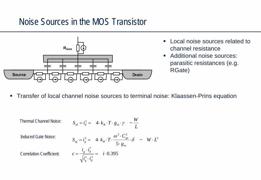
Thermal Channel Noise:
Induced Gate Noise:
Noise Sources in the MOS Transistor
Local noise sources related to channel resistanceAdditional noise sources: parasitic resistances (e.g. RGate)
Transfer of local channel noise sources to terminal noise: Klaassen-Prins equation
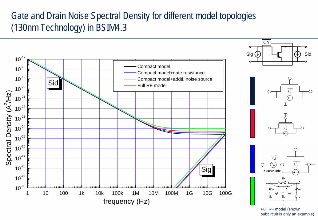
Gate and Drain Noise Spectral Density for different model topologies (130nm Technology) in BSIM4.3
Sig Sid
CY
1 10 100 1k 10k 100k 1M 10M 100M 1G 10G 100G10-30
10-29
10-28
10-27
10-26
10-25
10-24
10-23
10-22
10-21
10-20
10-19
10-18
10-17
Sig
Sid
Compact model Compact model+gate resistance Compact model+addtl. noise source Full RF model
Spe
ctra
l Den
sity
(A2 /H
z)
frequency (Hz)Full RF model (shown subcircuit is only an example)
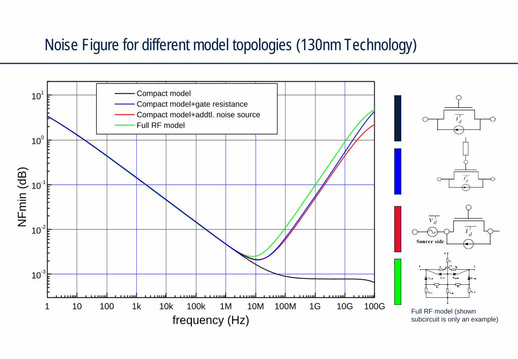
Noise Figure for different model topologies (130nm Technology)
1 10 100 1k 10k 100k 1M 10M 100M 1G 10G 100G
10-3
10-2
10-1
100
101 Compact model Compact model+gate resistance Compact model+addtl. noise source Full RF model
NFm
in (d
B)
frequency (Hz)Full RF model (shown subcircuit is only an example)
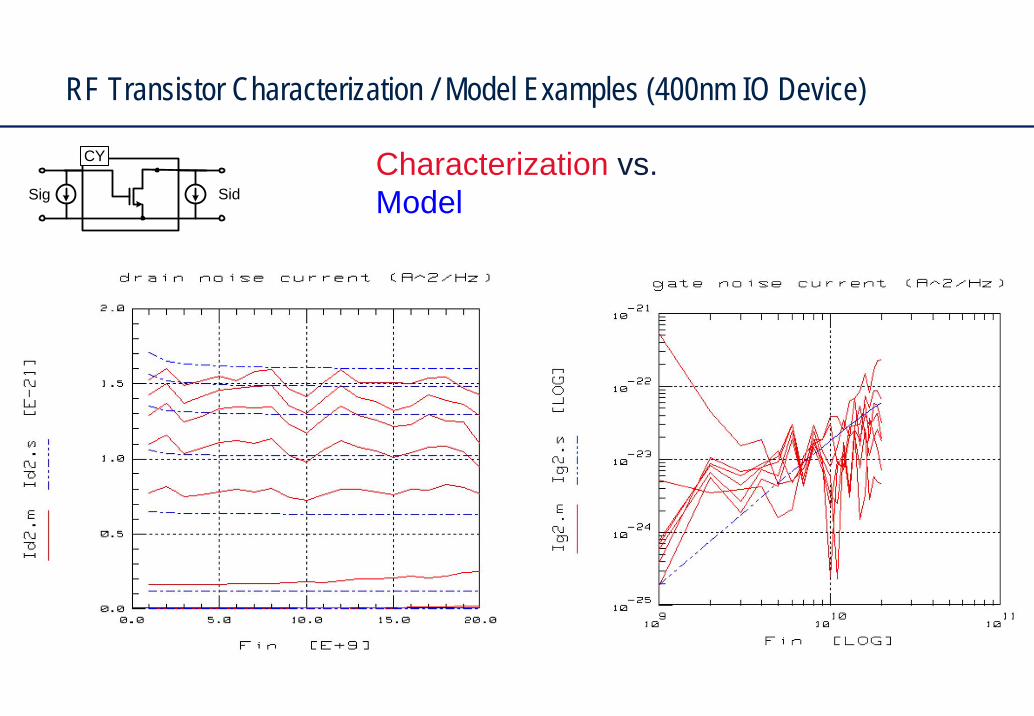
RF Transistor Characterization / Model Examples (400nm IO Device)
Sig Sid
CY Characterization vs.Model
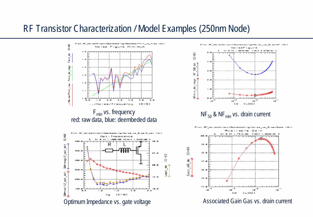
Associated Gain Gas vs. drain current
NF50 & NFmin vs. drain currentFmin vs. frequency red: raw data, blue: deembeded data
Optimum Impedance vs. gate voltage
R L
RF Transistor Characterization / Model Examples (250nm Node)
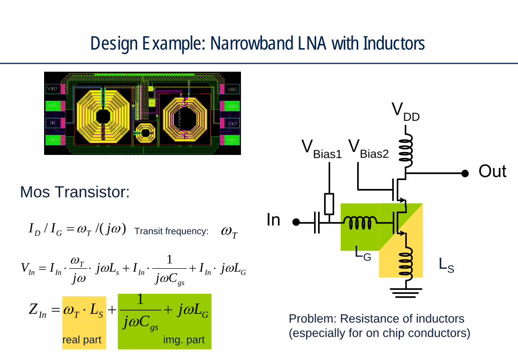
Design Example: Narrowband LNA with Inductors
Bias1 Bias2
DD
)/(/ ωω jII TGD =
GIngs
InsT
InIn LjICj
ILjj
IV ωω
ωωω
⋅+⋅+⋅⋅=1
Mos Transistor:
Ggs
STIn LjCj
LZ ωω
ω ++⋅=1
real part img. part
LSLG
Transit frequency: Tω
Problem: Resistance of inductors(especially for on chip conductors)
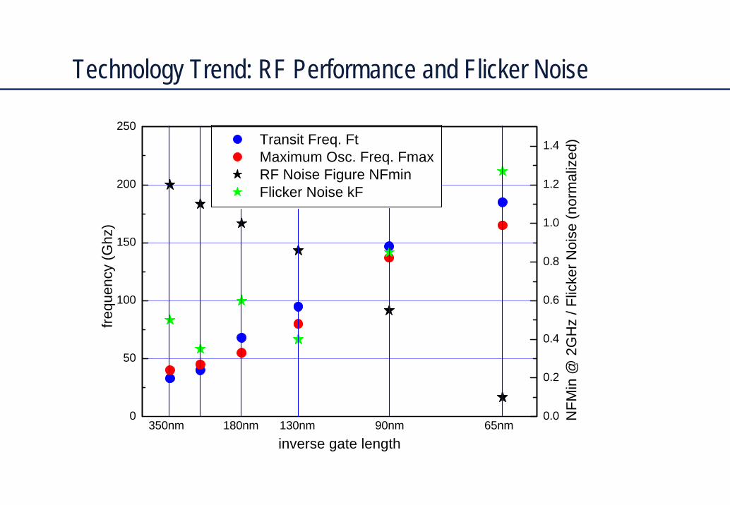
Technology Trend: RF Performance and Flicker Noise
0
50
100
150
200
250 Transit Freq. Ft Maximum Osc. Freq. Fmax RF Noise Figure NFmin Flicker Noise kF
frequ
ency
(Ghz
)
inverse gate length
0.0
0.2
0.4
0.6
0.8
1.0
1.2
1.4
NFM
in @
2G
Hz
/ Flic
ker N
oise
(nor
mal
ized
)
350nm 180nm 130nm 90nm 65nm

Summary Noise in Linear Amplifiers
Noise measurement is a narrowband power measurement.
Test system is basically a tunable low noise receiver.
Four noise parameters are necessary to model noise sources of a two port, many representations are used (and are equivalent).
Tuning of source impedance is necessary to characterize all noise parameters.
RF Circuit Noise Characterization : Outline
Overview:– Typical wireless architectures
– Importance of noise for wireless communication
– Semiconductor Noise Sources
Noise in Linear Amplifiers– Noise Figure, Noise Temperature, Noise
Measure
– NF Measurement
– Noise of Two-Ports
– Characterization of 4 Noise Pparameters
– LNA Example
Noise in Mixer Circuits– Mixer Introduction
– Cyclostationary Noise
– Gilbert Mixer
Noise in Oscillators– Basics and Requirements
– Hajimiri and Leeson Theory
– Typical VCO Circuit
– Characterization
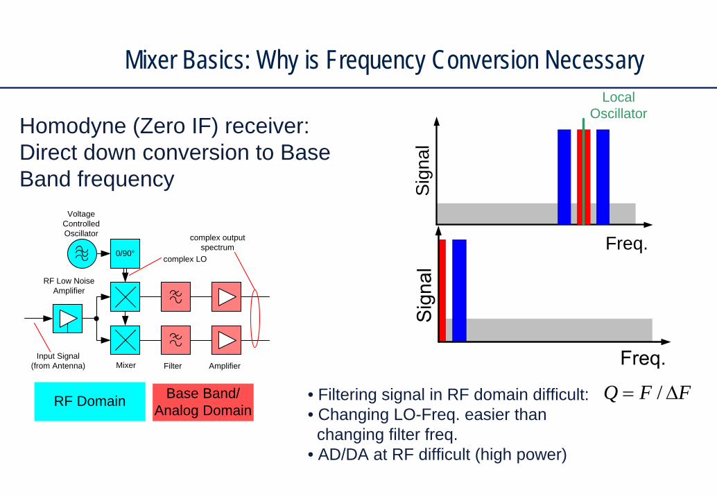
Mixer Basics: Why is Frequency Conversion Necessary
0/90°complex LO
Input Signal(from Antenna)
complex outputspectrum
Amplifier
Base Band/Analog Domain
RF Low NoiseAmplifier
VoltageControlledOscillator
Mixer Filter
RF Domain
Freq.
Sig
nal
LocalOscillator
Homodyne (Zero IF) receiver:Direct down conversion to Base Band frequency
• Filtering signal in RF domain difficult:• Changing LO-Freq. easier thanchanging filter freq.
• AD/DA at RF difficult (high power)
FFQ Δ= /
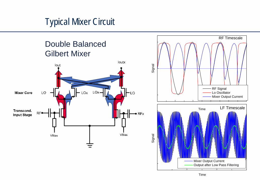
Typical Mixer Circuit
Double BalancedGilbert Mixer
LF Timescale
Sig
nal
Time
Mixer Output Current Output after Low Pass Filtering
RF Timescale
Sig
nal
Time
RF Signal Lo Oscillator Mixer Output Current
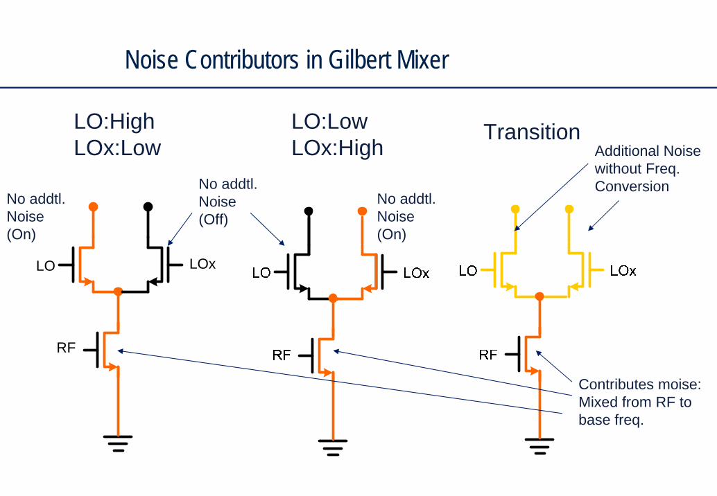
Noise Contributors in Gilbert Mixer
RF
LO LOx
LO:HighLOx:Low
LO:LowLOx:High
Transition
Contributes moise:Mixed from RF to base freq.
No addtl. Noise(On)
No addtl. Noise(Off)
No addtl. Noise(On)
Additional Noisewithout Freq. Conversion
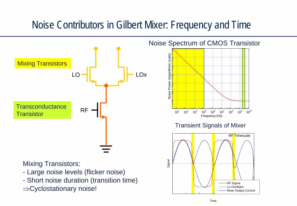
Noise Contributors in Gilbert Mixer: Frequency and Time
LOx
RF
LO
TransconductanceTransistor
Mixing Transistors
102 103 104 105 106 107 108 109 1010
Noi
se P
ower
(log
arith
mic
sca
le)
Frequency (Hz)
Noise Spectrum of CMOS Transistor
RF Timescale
Sig
nal
Time
RF Signal Lo Oscillator Mixer Output Current
Transient Signals of Mixer
Mixing Transistors:- Large noise levels (flicker noise)- Short noise duration (transition time)⇒Cyclostationary noise!
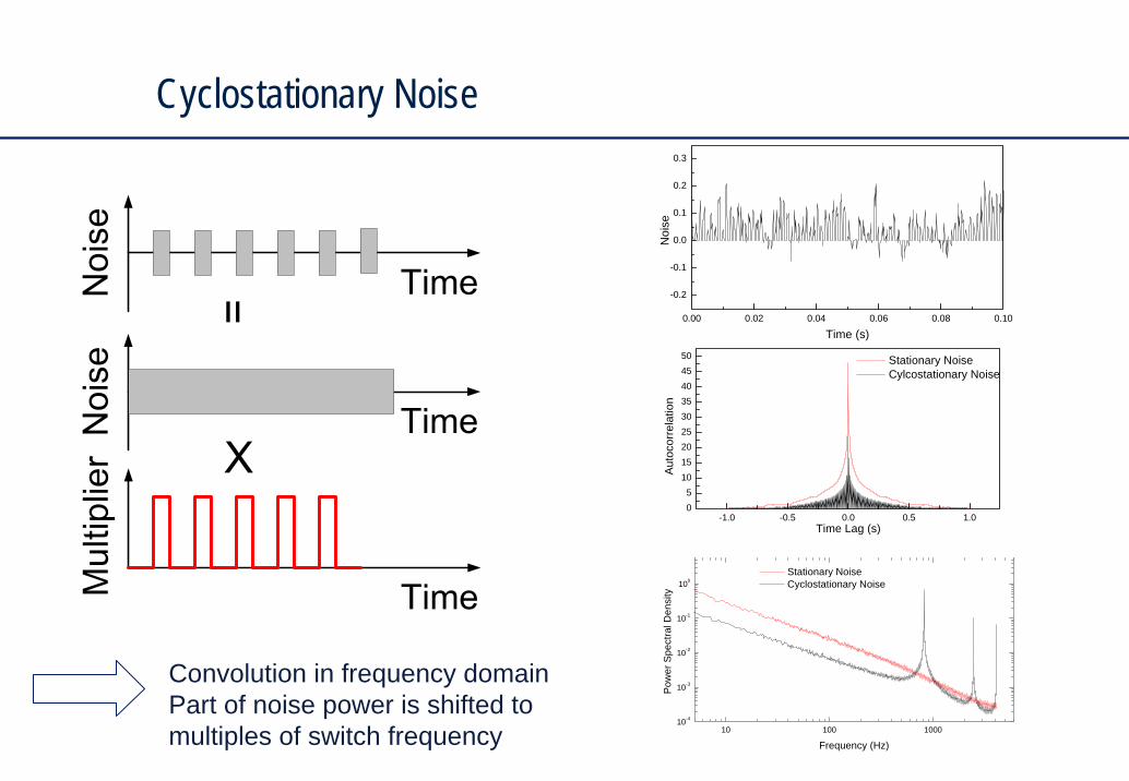
Cyclostationary Noise
0.00 0.02 0.04 0.06 0.08 0.10
-0.2
-0.1
0.0
0.1
0.2
0.3
Noi
se
Time (s)
-1.0 -0.5 0.0 0.5 1.005
101520253035404550 Stationary Noise
Cylcostationary Noise
Auto
corr
elat
ion
Time Lag (s)
10 100 100010-4
10-3
10-2
10-1
100 Stationary Noise Cyclostationary Noise
Frequency (Hz)
Pow
er S
pect
ral D
ensi
tyConvolution in frequency domainPart of noise power is shifted tomultiples of switch frequency
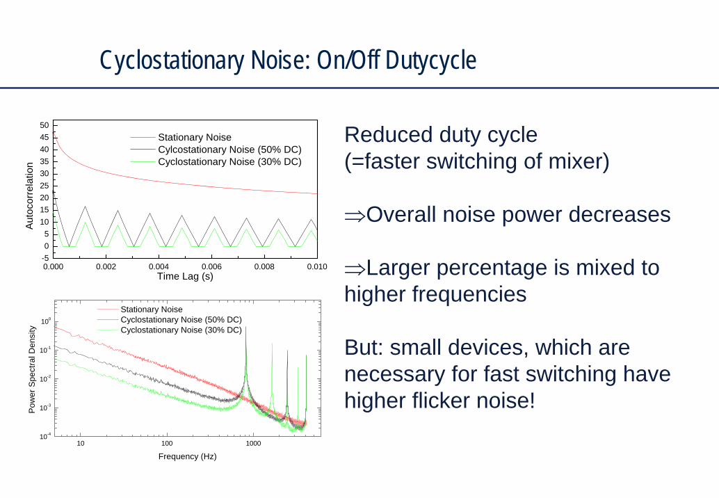
Cyclostationary Noise: On/Off Dutycycle
0.000 0.002 0.004 0.006 0.008 0.010-505
101520253035404550
Stationary Noise Cylcostationary Noise (50% DC) Cyclostationary Noise (30% DC)
Aut
ocor
rela
tion
Time Lag (s)
10 100 100010-4
10-3
10-2
10-1
100
Stationary Noise Cyclostationary Noise (50% DC) Cyclostationary Noise (30% DC)
Frequency (Hz)
Pow
er S
pect
ral D
ensi
ty
Reduced duty cycle (=faster switching of mixer)
⇒Overall noise power decreases
⇒Larger percentage is mixed to higher frequencies
But: small devices, which are necessary for fast switching have higher flicker noise!
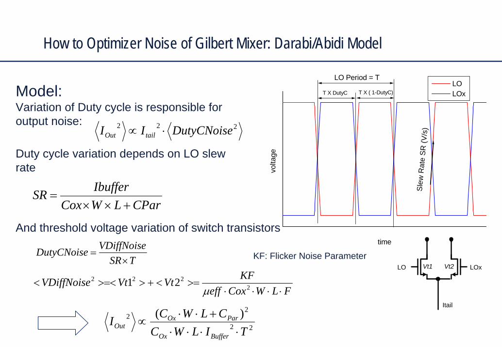
How to Optimizer Noise of Gilbert Mixer: Darabi/Abidi Model
Slew
Rat
e SR
(V/s
)
T X ( 1-DutyC)T X DutyC
LO Period = T LO LOx
volta
ge
time
LO LOx
Itail
Vt1 Vt2
FLWCoxeffKFVtVtVDiffNoise
⋅⋅⋅⋅>=<+>>=<< 2
222 21μ
Model: Variation of Duty cycle is responsible for output noise:
Duty cycle variation depends on LO slew rate
TSRVDiffNoiseDutyCNoise
×= KF: Flicker Noise Parameter
CParLWCoxIbufferSR
+××=
And threshold voltage variation of switch transistors
222 DutyCNoiseII tailOut ⋅∝
22
22 )(
TILWCCLWCI
BufferOx
ParOxOut ⋅⋅⋅⋅
+⋅⋅∝
22
22 )(
TILWCCLWCI
BufferOx
ParOxOut ⋅⋅⋅⋅
+⋅⋅∝
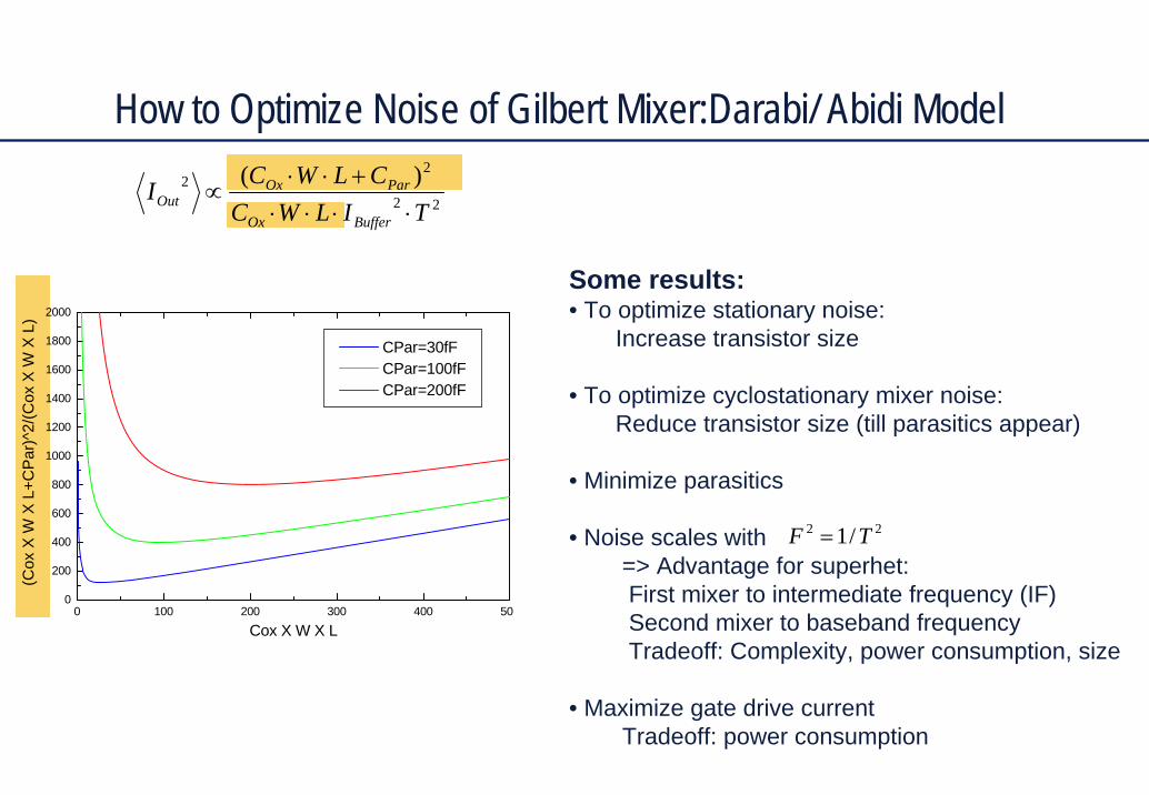
0 100 200 300 400 5000
200
400
600
800
1000
1200
1400
1600
1800
2000
CPar=30fF CPar=100fF CPar=200fF
(Cox
X W
X L
+CP
ar)^
2/(C
ox X
W X
L)
Cox X W X L
Some results:• To optimize stationary noise:
Increase transistor size
• To optimize cyclostationary mixer noise:Reduce transistor size (till parasitics appear)
• Minimize parasitics
• Noise scales with=> Advantage for superhet: First mixer to intermediate frequency (IF) Second mixer to baseband frequencyTradeoff: Complexity, power consumption, size
• Maximize gate drive current Tradeoff: power consumption
22 /1 TF =
How to Optimize Noise of Gilbert Mixer:Darabi/ Abidi Model
RF Circuit Noise Characterization : OutlineOverview:
– Typical wireless architectures
– Importance of noise for wireless communication
– Semiconductor Noise Sources
Noise in Linear Amplifiers– Noise Figure, Noise Temperature, Noise
Measure
– NF Measurement
– Noise of Two-Ports
– Characterization of 4 Noise Parameters
– LNA Example
Noise in Mixer Circuits– Mixer Introduction
– Cyclostationary Noise
– Gilbert Mixer
Noise in Oscillators– Basics and Requirements
– Hajimiri and Leeson Theory
– Typical VCO Circuit
– Characterization
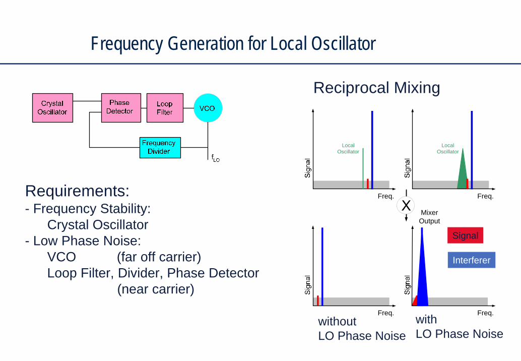
Frequency Generation for Local Oscillator
withoutLO Phase Noise
withLO Phase Noise
Freq.
LocalOscillator
Freq.
LocalOscillator
Freq. Freq.
MixerOutput
Reciprocal Mixing
Requirements:- Frequency Stability:
Crystal Oscillator- Low Phase Noise:
VCO (far off carrier)Loop Filter, Divider, Phase Detector
(near carrier)
Signal
Interferer
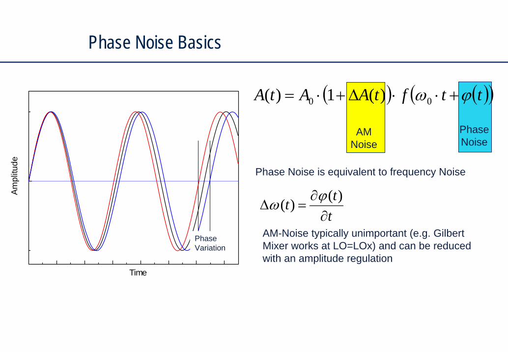
Phase Noise Basics
PhaseNoise
AMNoise
( ) ( )( )ttftAAtA ϕω +⋅⋅Δ+⋅= 00 )(1)(
Am
plitu
de
Time
Phase Variation
ttt
∂∂
=Δ)()( ϕω
Phase Noise is equivalent to frequency Noise
AM-Noise typically unimportant (e.g. Gilbert Mixer works at LO=LOx) and can be reduced with an amplitude regulation
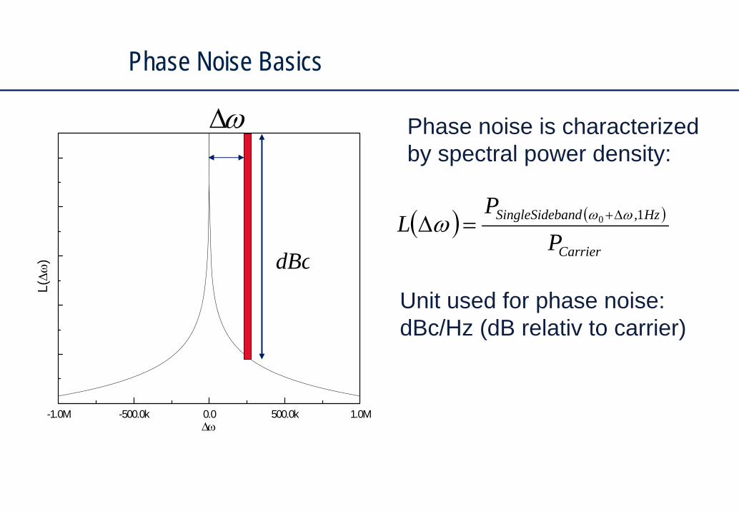
Phase Noise Basics
( ) ( )
Carrier
HzbandSingleSide
PP
L 1,0 ωωω Δ+=Δ
Unit used for phase noise:dBc/Hz (dB relativ to carrier)
ωΔ
-1.0M -500.0k 0.0 500.0k 1.0M
L(Δω
)
Δω
dBc
Phase noise is characterizedby spectral power density:
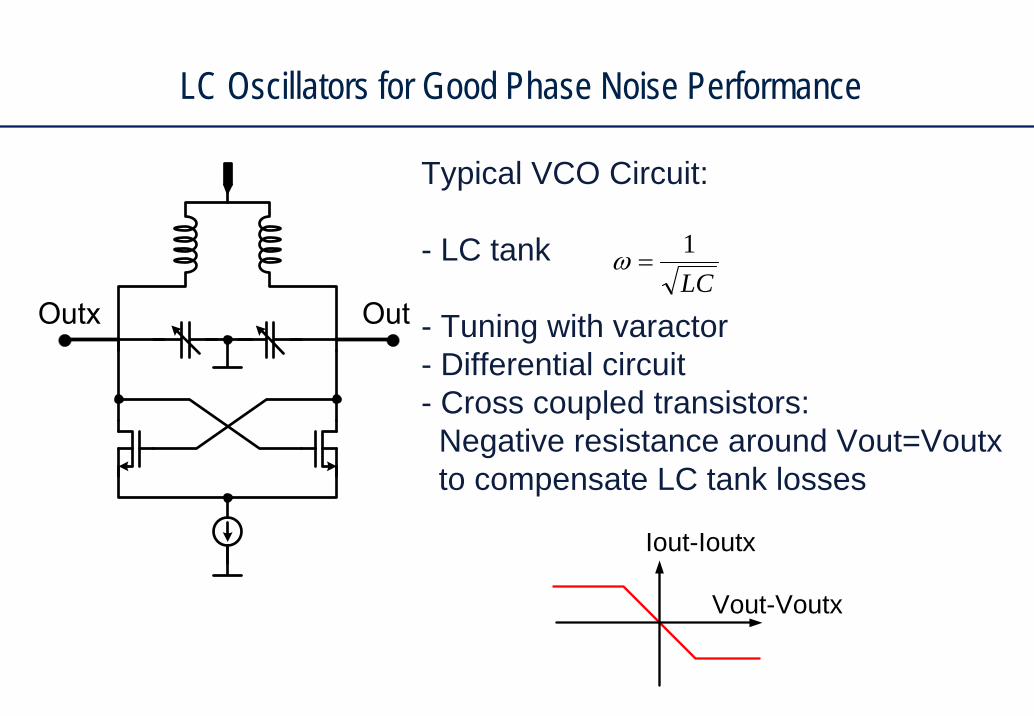
LC Oscillators for Good Phase Noise Performance
LC1
=ω
Typical VCO Circuit:
- LC tank
- Tuning with varactor- Differential circuit- Cross coupled transistors:Negative resistance around Vout=Voutxto compensate LC tank losses
Vout-Voutx
Iout-Ioutx
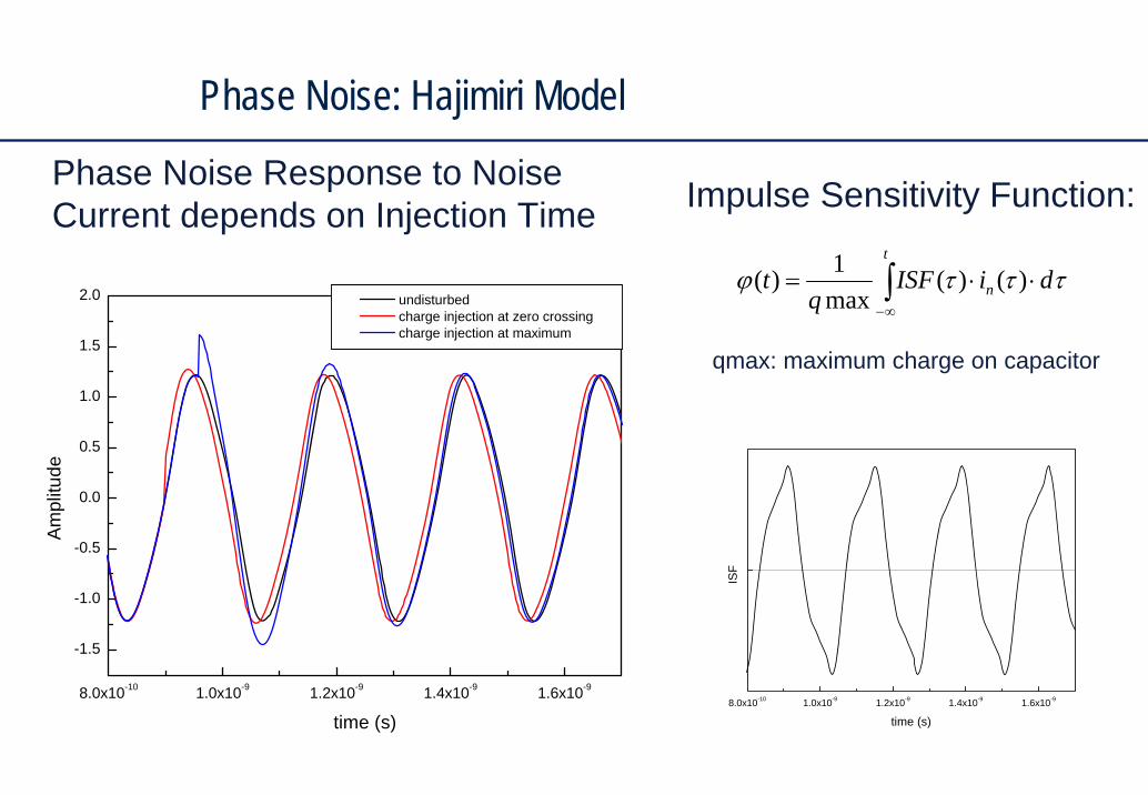
Phase Noise: Hajimiri Model
8.0x10⁻¹⁰ 1.0x10⁻⁹ 1.2x10⁻⁹ 1.4x10⁻⁹ 1.6x10⁻⁹
-1.5
-1.0
-0.5
0.0
0.5
1.0
1.5
2.0
Ampl
itude
time (s)
undisturbed charge injection at zero crossing charge injection at maximum
8.0x10⁻¹⁰ 1.0x10⁻⁹ 1.2x10⁻⁹ 1.4x10⁻⁹ 1.6x10⁻⁹
ISF
time (s)
Phase Noise Response to Noise Current depends on Injection Time Impulse Sensitivity Function:
∫∞−
⋅⋅=t
n diISFq
t τττϕ )()(max1)(
qmax: maximum charge on capacitor
Phase Noise: Leesons Heuristic Model
( )⎥⎥⎦
⎤
⎢⎢⎣
⎡
⎟⎟⎠
⎞⎜⎜⎝
⎛
Δ
Δ+⋅
⎟⎟
⎠
⎞
⎜⎜
⎝
⎛⎟⎟⎠
⎞⎜⎜⎝
⎛Δ⋅⋅
+⋅⋅⋅⋅
⋅=Δω
ω
ωωω
3/12
0 12
12log10 f
Carrier QPTkFL
103 104 105 106 107 108 109 1010
Leeson‘s Heuristic Formula (1966)
L(Δω
) dB
c/H
z
Δω (Hz)
Flicker NoiseCorner Frequency Oscillator Optimization:
Q
PCarrier
B. Razavi, „RF Microelectronics“, Prentice Hall 1998
M. Golio, „Microwave and RF Product Applications“, CRC Press 2003
S.A. Maas, „Noise in Linear and Nonlinear Circuits“, Artech House 2005
H.T. Friis, „Noise figures of radio receivers“, Proc. IRE, vol 32, 1944, pp. 419-422
Agilent Application Notes: 95-1,57-1,57-2,57-3
V. Adamian, A. Uhlir Jr., „A novel procedure for receiver noise characterization“, IEEE Trans. on Instr. Meas.,1973 ,pp 181-182
L. F. Tiemeijer, R.J. Havens, R. de Kort, A. J. Scholten, „Improved Y-Factor Method for Wide-Band On-Wafer Noise Parameter Measurements“, IEEE Trans. on Microwave Theory and Techniques, Vol. 53, No.9, 2005, pp. 2917-2925
H. Hillbrand, P. Russer, „An Efficient Method for Computer Aided Noise Analysis of Linear Amplifier Networks“, IEEE Trans. on Circuits and Systems, Vol. Cas. 23, No. 4, 1976, pp 235-238
J. Engberg, T. Larsen, „Noise Theory of Linear and Nonlinear Circuits“, Wiley 1995
T.H. Lee, „The Design of CMOS Radio-Frequency Integrated Circuits“, Cambridge 2004 (second edition)
http://www.designers-guide.org/Theory/cyclo-pub.ppt
H. Darabi, A. Abidi, „Noise in RF-CMOS Mixers: A Simple Physical Model“, IEEE Trans. Solid State Circuits, vol. 35, no.1, 2000, pp. 15-25
E. Hegarzi, J. Rael, A. Abidi, „High-Purity Oscillators“, Kluwer Academic Publishers 2005
M. Tiebout, „Low Power VCO Design in CMOS Low Power VCO Design in CMOS“, Springer 2005
A. Hajimiri, T.H. Lee, A General Theory of Phase Noise in Electrical Oscillators, IEEE Journal of Solid-State Circuits, Vol. 33, No. 2, 1988, pp 179-194
D.B. Leeson, “A simple model of feedback oscillator noise spectrum”, Proc. IEEE, vol. 54, 1966, pp.329-330
Literature