research article improving breakdown voltage for a...
TRANSCRIPT
Research ArticleImproving Breakdown Voltage for aNovel SOI LDMOS with a Lateral Variable Doping Profile onthe Top Interface of the Buried Oxide Layer
Jingjing Jin,1 Shengdong Hu,1,2 Yinhui Chen,1 Kaizhou Tan,2 Jun Luo,2 Feng Zhou,1
Zongze Chen,1 and Ye Huang1
1College of Communication Engineering, Chongqing University, Chongqing 400044, China2National Laboratory of Analogue Integrated Circuits, No. 24 Research Institute of China Electronics Technology Group Corporation,Chongqing 400060, China
Correspondence should be addressed to Shengdong Hu; [email protected]
Received 13 January 2015; Revised 27 May 2015; Accepted 28 June 2015
Academic Editor: Wai Tung Ng
Copyright © 2015 Jingjing Jin et al. This is an open access article distributed under the Creative Commons Attribution License,which permits unrestricted use, distribution, and reproduction in any medium, provided the original work is properly cited.
In order to achieve a high breakdown voltage (BV) for the SOI (Silicon-On-Insulator) power device in high voltage ICs, a novelhigh voltage n-channel lateral double-diffused MOS (LDMOS) with a lateral variable interface doping profile (LVID) placed atthe interface between the SOI layer and the buried-oxide (BOX) layer (LVID SOI) is researched. Its breakdown mechanism isinvestigated theoretically, and its structure parameters are optimized and analyzed by 2D simulation software MEDICI. In the highvoltage blocking state, the high concentration ionized donors in the depleted LVIDmake the surface electric field of SOI layer (𝐸
𝑆)
more uniform and enhance the electric field of BOX layer (𝐸𝐼), which can prevent the lateral premature breakdown and result
in a higher BV. Compared with the conventional uniformly doped (UD) SOI LDMOS, 𝐸𝐼of the optimized LVID SOI LDMOS is
enhanced by 79% from 119V/𝜇m to 213V/𝜇m, and BV is increased by 33.4% from 169V to 227V. Simulations indicate that themethod of LVID profile can significantly improve breakdown voltage for the SOI LDMOS.
1. Introduction
SOI technology has been widely used in high voltage ICs dueto its advantages such as superior isolation, high speed, andlow loss [1]. However, SOI power devices suffer from a lowvertical BV. A feasible way to increase the BV is to enhancethe dielectric layer field (ENDIF), and several new struc-tures have been proposed by ENDIF, in which introducinginterface charges is effective and attractive [2]. The variabledoping profile is a method of introducing interface chargeswhich was firstly proposed to avoid high voltage breakdownfor planar junctions in 1985 [3]. The approach of designingand implementing the linear doping profile on thin SOI forlateral high voltage devices was presented in 1995 [4]. Asubmicron thin film SOI LDMOS with the variable dopingprofile and numericalmodeling of linear doping profiles wereproposed in 1996 and 1999, respectively [5, 6]. After 2000,
several new SOI devices structures with linear doping profilewere proposed [7–11].
In this paper, a novel SOI device with a LVID profile(LVID SOI LDMOS) is designed. The doping profile of driftregion is a combination of linear variable doping and uniformdoping in vertical dimension, which is different from theabove-mentioned structures.The influence of the parameterson BV and the specific on-resistance (𝑅on,sp) is presented.Thesimulated results indicate that themethod of LVIDprofile cansignificantly improve BV compared with UD profile.
2. Structure and Mechanism
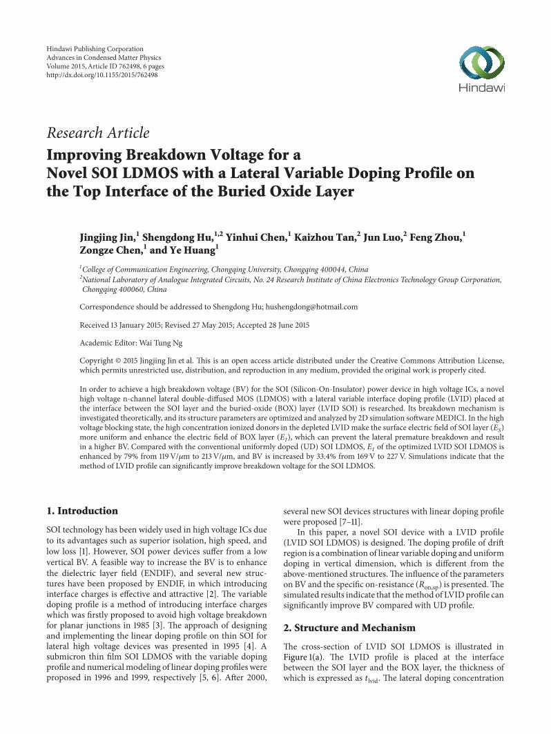
The cross-section of LVID SOI LDMOS is illustrated inFigure 1(a). The LVID profile is placed at the interfacebetween the SOI layer and the BOX layer, the thickness ofwhich is expressed as 𝑡lvid. The lateral doping concentration
Hindawi Publishing CorporationAdvances in Condensed Matter PhysicsVolume 2015, Article ID 762498, 6 pageshttp://dx.doi.org/10.1155/2015/762498
2 Advances in Condensed Matter Physics
p-well
P-substrate
Variable doping profile
x
y
S G D
M
N
p+ n+n+
n-type Nd
SiO2
ts
tlvid
tI
tsub
Ld
Lpw
Uniform doping
(a)
Drain
C(x)
(cm
−3)
C0
x (𝜇m)
CLd
(b)
Figure 1: LVID SOI LDMOS. (a) Schematic cross-section; (b) the doping concentration of the LVID profile.
of the LVID profile is shown in Figure 1(b), which can beexpressed as
𝐶 (𝑥) = 𝐺𝑥+𝐶0, (1)
where 𝑥 is the distance away from source, 𝐺 is the lineargraded coefficient which determines the slope of the profile,𝐶(𝑥) is the doping concentration of LVID profile, and 𝐶0 isthe doping concentration at 𝑥 = 0, 𝑦 = 𝑡𝑠. Here, 𝑡𝑠 is thethickness of the SOI layer and𝑁𝑑 is the doping concentrationof uniform doping section.
According to Figure 1(b) and (1),
𝐺 =
𝐶𝐿𝑑− 𝐶0
𝐿𝑑
, (2)
where𝐶𝐿𝑑is the doping concentration at𝑥 = 𝐿
𝑑,𝑦 = 𝑡
𝑠. Since
𝐶0ismuch less than𝐶
𝐿𝑑, it is ignored in the above expression.
𝐺 is proportional to 𝐶𝐿𝑑.
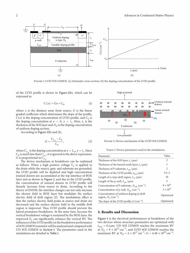
The device mechanism at breakdown can be explainedas follows. When a high positive voltage 𝑉
𝑑is applied to
the drain while the source, gate, and substrate are grounded,the LVID profile will be depleted and high concentrationionized donors are accumulated at the top interface of BOXlayer just as shown in Figure 2, and due to the LVID profile,the concentration of ionized donors in LVID profile willlinearly increase from source to drain. According to thetheory of ENDIF, the interface charges can not only increasethe electric field in BOX layer but modulate the surfaceelectric field of drift region [2]. The modulation effect isthat the surface electric field peaks at source and drain aredecreased and the surface electric field in the middle driftregion is improved. Thus LVID profile should prevent thelateral premature breakdown. At the same time, because thevertical breakdown voltage is sustained by the BOX layer, theimproved 𝐸
𝐼can significantly enhance the vertical BV. The
influences of the LVIDprofile on the breakdownperformanceof SOI LDMOS transistorwill be analyzed and comparedwithUD SOI LDMOS in Section 3. The parameters used in thesimulations are detailed in Table 1.
P-substrate
High potential
Low potential
donors
Uniform ionizeddonors
SiO2
ΔEI
Linear ionized
Figure 2: Device mechanism of the LVID SOI LDMOS.
Table 1: Device parameters used in the simulations.
Parameter ValueThickness of the SOI layer, 𝑡
𝑠(𝜇m) 2
Thickness of the buried oxide layer, 𝑡𝐼(𝜇m) 1
Thickness of P-substrate, 𝑡sub (𝜇m) 2Thickness of the LVID profile, 𝑡lvid (𝜇m) 0.1–2Length of n-type drift region, 𝐿
𝑑(𝜇m) 10
Length of the p-well, 𝐿pw (𝜇m) 5Concentration of P-substrate,𝑁sub (cm
−3) 8 × 10¹⁴
Concentration of p-well,𝑁pw (cm−3) 3 × 10¹⁶
Concentration of uniform doping in driftregion,𝑁
𝑑(cm−3) Optimized
The slope of the LVID profile, 𝐺 (cm−4) Optimized
3. Results and Discussion
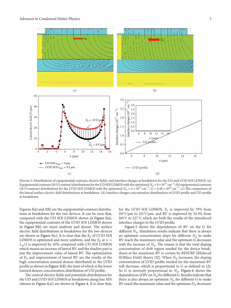
Figure 3 is the electrical performances at breakdown of thetwo devices whose structure parameters are optimized with𝑡lvid = 0.1 𝜇m. UD SOI LDMOS reaches the maximum BVat 𝑁𝑑= 9 × 1015 cm−3, and LVID SOI LDMOS reaches the
maximum BV at 𝑁𝑑= 4 × 1015 cm−3, 𝐺 = 4.48 × 1020 cm−4.
Advances in Condensed Matter Physics 3
ES
(a)
ES
(b)
0 2 4 6 8 10 12 14 160
10
20
30
40
50
Late
ral e
lect
ric fi
eld
(V/𝜇
m)
UD SOI tlvid = 0𝜇mLVID SOI tlvid = 0.1 𝜇m
ES = 19V/𝜇m
ES = 9V/𝜇m
x (𝜇m)
(c)
6 8 10 12 14 160.0
0.5
1.0
1.5
2.0
2.5
3.0
0.00.51.01.52.02.53.0
LVID profile
6 10 12 14 16
UD profile
x (𝜇m)
x (𝜇m)
Inte
rface
char
ges(10
17cm
−3)
8
Inte
rface
char
ges (10
17cm
−3)
(d)
Figure 3: Distributions of equipotential contours, electric fields, and interface charges at breakdown for the UD and LVID SOI LDMOS. (a)Equipotential contours (10V/contour) distributions for theUDSOILDMOSwith the optimized𝑁
𝑑=9× 1015 cm−3; (b) equipotential contours
(10V/contour) distributions for the LVID SOI LDMOS with the optimized𝑁𝑑= 4 × 1015 cm−3, 𝐺 = 4.48 × 1020 cm−4. (c) The comparison of
the lateral surface electric field distributions at breakdown. (d) Interface charges concentration distributions of LVID profile and UD profileat breakdown.
Figures 3(a) and 3(b) are the equipotential contours distribu-tions at breakdown for the two devices. It can be seen that,compared with the UD SOI LDMOS shown in Figure 3(a),the equipotential contours of the LVID SOI LDMOS shownin Figure 3(b) are more uniform and denser. The surfaceelectric field distributions at breakdown for the two devicesare shown in Figure 3(c). It is clear that the 𝐸𝑆 of LVID SOILDMOS is optimized and more uniform, and the 𝐸𝑆 at 𝑥 =𝐿𝑑/2 is improved by 111% compared with UD SOI LDMOSwhich means an increase of lateral BV, and the shadow part isjust the improvement value of lateral BV. The optimizationof 𝐸𝑆and improvement of lateral BV are the results of the
high concentration ionized donors distributed in the LVIDprofile as shown in Figure 3(d), the inset of which is the lowerionized donors concentration distribution of UD profile.
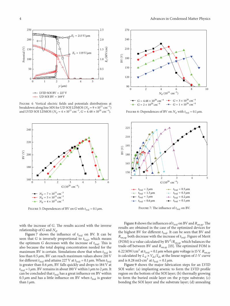
The vertical electric fields and potentials distributions forthe UD and LVID SOI LDMOS at breakdown along line MN(shown in Figure 1(a)) are shown in Figure 4. It is clear that,
for the LVID SOI LDMOS, 𝐸𝐼is improved by 79% from
119V/𝜇m to 213V/𝜇m, and BV is improved by 34.3% from169V to 227V, which are both the results of the introducedinterface charges in the LVID profile.
Figure 5 shows the dependences of BV on the 𝐺 fordifferent 𝑁𝑑. Simulation results indicate that there is alwaysan optimum concentration slope for different 𝑁𝑑 to makeBV reach the maximum value and the optimum 𝐺 decreaseswith the increase of 𝑁𝑑. The reason is that the total dopingconcentration of drift region needed for the device break-down at the maximum BV is certain by RESURF (REducedSURface Field) theory [12]. When 𝑁
𝑑increases, the doping
concentration of LVID profile needed for the maximum BVwill decrease, which is proportional to 𝐺 as defined in (2).So 𝐺 is inversely proportional to 𝑁
𝑑. Figure 6 shows the
dependences of BVon𝑁𝑑for different𝐺. Results indicate that
there is also always an optimum 𝑁𝑑for different 𝐺 to make
BV reach themaximum value and the optimum𝑁𝑑decreases
4 Advances in Condensed Matter Physics
0 1 2 3 4 50
50
100
150
200
250
0.0
0.5
1.0
1.5
2.0
2.5
Pote
ntia
l (V
)
y (𝜇m)
LVID SOI BV = 227VUD SOI BV = 169V
EI = 213V/𝜇m
EI = 119V/𝜇m
EI
(MV
/cm
)Figure 4: Vertical electric fields and potentials distributions atbreakdown along lineMN for UD SOI LDMOS (𝑁
𝑑= 9 × 1015 cm−3)
and LVID SOI LDMOS (𝑁𝑑= 4 × 1015 cm−3, 𝐺 = 4.48 × 1020 cm−4).
0 1 2 3 4 5 6160
180
200
220
240
BV (V
)
Nd = 7 × 1015 cm−3
Nd = 5 × 1015 cm−3
Nd = 4 × 1015 cm−3
G (1020 cm−4)
Figure 5: Dependences of BV on 𝐺 with 𝑡lvid = 0.1 𝜇m.
with the increase of 𝐺. The results accord with the inverserelationship of 𝐺 and𝑁𝑑.
Figure 7 shows the influence of 𝑡lvid on BV. It can beseen that 𝐺 is inversely proportional to 𝑡lvid, which meansthe optimum 𝐺 decreases with the increase of 𝑡lvid. This isalso because the total doping concentration needed for themaximum BV is certain. Simulations show that when 𝑡lvid isless than 0.5 𝜇m, BV can reach maximum values above 210Vfor different 𝑡lvid and attains 227V at 𝑡lvid = 0.1 𝜇m.When 𝑡lvidis greater than 0.6𝜇m, BV falls quickly and drops to 184V at𝑡lvid = 1 𝜇m. BV remains in about 180Vwithin 1 𝜇m to 2 𝜇m. Itcan be concluded that 𝑡lvid has a great influence on BV within0.5 𝜇m and has a little influence on BV when 𝑡lvid is greaterthan 1 𝜇m.
0 2 4 6 8 1090
120
150
180
210
240
270
BV (V
)
G = 4.48 × 1020 cm−4
G = 2 × 1020 cm−4G = 3 × 1020 cm−4
G = 1 × 1020 cm−4
Nd (1015 cm−3)
Figure 6: Dependences of BV on𝑁𝑑with 𝑡lvid = 0.1 𝜇m.
0 1 2 3 4 5
150
165
180
195
210
225
BV (V
)
G (1020 cm−4)
tlvid = 2𝜇mtlvid = 1.5 𝜇mtlvid = 1𝜇mtlvid = 0.6 𝜇m
tlvid = 0.5 𝜇mtlvid = 0.3 𝜇mtlvid = 0.2 𝜇mtlvid = 0.1 𝜇m
Figure 7: The influence of 𝑡lvid on BV.
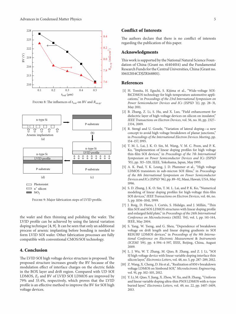
Figure 8 shows the influences of 𝑡lvid on BV and𝑅on,sp.Theresults are obtained in the case of the optimized devices forthe highest BV for different 𝑡lvid. It can be seen that BV and𝑅on,sp both decrease with the increase of 𝑡lvid. Figure of Merit(FOM) is a value calculated by BV2/𝑅on,sp which balances thetrade-off between BV and 𝑅on,sp [13]. The optimized FOM is6.22MW/cm2 at 𝑡lvid = 0.1 𝜇mwhen gate voltage is 15 V. 𝑅on,spis calculated by 𝐿
𝑑× 𝑉𝑑𝑠/𝐼𝑑𝑠at the linear region of 𝐼-𝑉 curve
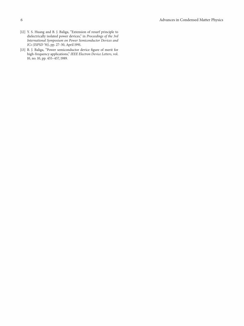
and is 8.28mΩ⋅cm2 at 𝑡lvid = 0.1 𝜇m.Figure 9 shows the major fabrication steps for an LVID
SOI wafer: (a) implanting arsenic to form the LVID profileregion on the bottom of the SOI layer; (b) thermally growingto form the buried oxide layer on the p-type substrate; (c)bonding the SOI layer and the substrate layer; (d) annealing
Advances in Condensed Matter Physics 5
0.1 0.2 0.3 0.4 0.5
210
213
216
219
222
225
228
7.6
7.8
8.0
8.2
8.4
tlvid (𝜇m)
Ron
,sp
(mΩ·c
m2)
BV (V
)
Figure 8: The influences of 𝑡lvid on BV and 𝑅on,sp.
n-type Si
Arsenic implantation(a)
P-substrate
(c)
n-type SiLVID profilen-type Si
LVID profile
P-substrate
(d)
P-substrate
(b)
Photoresist
SiO2
n+ silicon
Figure 9: Major fabrication steps of LVID profile.
the wafer and then thinning and polishing the wafer. TheLVID profile can be achieved by using the lateral variationdoping technique [4, 9]. It can be seen that only an additionalprocess of arsenic implanting before bonding is needed toform LVID SOI wafer. Other fabrication processes are fullycompatible with conventional CMOS/SOI technology.
4. Conclusion
The LVID SOI high voltage device structure is proposed.Theproposed structure increases greatly the BV because of themodulation effect of interface charges on the electric fieldsin the BOX layer and drift region. Compared with UD SOILDMOS, 𝐸
𝐼and BV of LVID SOI LDMOS are improved by
79% and 33.4%, respectively, which proves that the LVIDprofile is an effective method to improve the BV for SOI highvoltage devices.
Conflict of Interests
The authors declare that there is no conflict of interestsregarding the publication of this paper.
Acknowledgments
Thiswork is supported by theNational Natural Science Foun-dation of China (Grant no. 61404014) and the FundamentalResearch Funds for theCentralUniversities, China (Grant no.106112014CDJZR168801).
References
[1] H. Tomita, H. Eguchi, S. Kijima et al., “Wide-voltage SOI-BiCDMOS technology for high-temperature automotive appli-cations,” in Proceedings of the 23rd International Symposium onPower Semiconductor Devices and ICs (ISPSD ’11), pp. 28–31,May 2011.
[2] B. Zhang, Z. Li, S. Hu, and X. Luo, “Field enhancement fordielectric layer of high-voltage devices on silicon on insulator,”IEEE Transactions on Electron Devices, vol. 56, no. 10, pp. 2327–2334, 2009.
[3] R. Stengl and U. Gosele, “Variation of lateral doping—a newconcept to avoid high voltage breakdown of planar junctions,”in Proceedings of the International Electron Devices Meeting, pp.154–157, 1995.
[4] T. M. L. Lai, J. K. O. Sin, M. Wang, V. M. C. Poon, and P. K.Ko, “Implemention of linear doping profiles for high voltagethin-film SOI devices,” in Proceedings of the 7th InternationalSymposium on Power Semiconductor Devices and ICs (ISPSD’95), pp. 315–320, IEEE, Yokohama, Japan, May 1995.
[5] A. K. Paul, Y. K. Leung, J. D. Plummer et al., “High voltageLDMOS transistors in sub-micron SOI films,” in Proceedingsof the 8th International Symposium on Power SemiconductorDevices and ICs (ISPSD ’96), pp. 89–92,Maui,Hawaii,USA,May1996.
[6] S. D. Zhang, J. K. O. Sin, T. M. L. Lai, and P. K. Ko, “Numericalmodeling of linear doping profiles for high-voltage thin-filmSOI devices,” IEEE Transactions on Electron Devices, vol. 46, no.5, pp. 1036–1041, 1999.
[7] J. Roig, D. Flores, I. Cortes, S. Hidalgo, and J. Millan, “Thinfilm SOI and SOS LDMOS structures with linear doping profileand enlarged field plate,” in Proceedings of the 24th InternationalConference on Microelectronics (MIEL ’04), vol. 1, pp. 141–144,IEEE, May 2004.
[8] S. Yang, W. Tseng, and G. Sheu, “Dependence of breakdownvoltage on drift length and linear doping gradients in SOIRESURF LDMOS devices,” in Proceedings of the 9th Interna-tional Conference on Electronic Measurement & Instruments(ICEMI ’09), pp. 4-594–4-597, IEEE, Beijing, China, August2009.
[9] L. J. Wu, W. T. Zhang, M. Qiao, B. Zhang, and Z. J. Li, “SOISJ high voltage device with linear variable doping interface thinsilicon layer,” Electronics Letters, vol. 48, no. 5, pp. 287–289, 2012.
[10] Z.Wang,X.Cheng,D.He et al., “Realization of 850 v breakdownvoltage LDMOS on Simbond SOI,”Microelectronic Engineering,vol. 91, pp. 102–105, 2012.
[11] Y. Li,M.Qiao, Y. Jiang, X. Zhou,W. Xu, and B. Zhang, “Uniformand linear variable doping ultra-thin PSOI LDMOSwith n-typeburied layer,” Electronics Letters, vol. 49, no. 22, pp. 1407–1409,2013.
6 Advances in Condensed Matter Physics
[12] Y. S. Huang and B. J. Baliga, “Extension of resurf principle todielectrically isolated power devices,” in Proceedings of the 3rdInternational Symposium on Power Semiconductor Devices andICs (ISPSD ’91), pp. 27–30, April 1991.
[13] B. J. Baliga, “Power semiconductor device figure of merit forhigh-frequency applications,” IEEE Electron Device Letters, vol.10, no. 10, pp. 455–457, 1989.

Submit your manuscripts athttp://www.hindawi.com
Hindawi Publishing Corporationhttp://www.hindawi.com Volume 2014
High Energy PhysicsAdvances in
The Scientific World JournalHindawi Publishing Corporation http://www.hindawi.com Volume 2014
Hindawi Publishing Corporationhttp://www.hindawi.com Volume 2014
FluidsJournal of
Atomic and Molecular Physics
Journal of
Hindawi Publishing Corporationhttp://www.hindawi.com Volume 2014
Hindawi Publishing Corporationhttp://www.hindawi.com Volume 2014
Advances in Condensed Matter Physics
OpticsInternational Journal of
Hindawi Publishing Corporationhttp://www.hindawi.com Volume 2014
Hindawi Publishing Corporationhttp://www.hindawi.com Volume 2014
AstronomyAdvances in
International Journal of
Hindawi Publishing Corporationhttp://www.hindawi.com Volume 2014
Superconductivity
Hindawi Publishing Corporationhttp://www.hindawi.com Volume 2014
Statistical MechanicsInternational Journal of
Hindawi Publishing Corporationhttp://www.hindawi.com Volume 2014
GravityJournal of
Hindawi Publishing Corporationhttp://www.hindawi.com Volume 2014
AstrophysicsJournal of
Hindawi Publishing Corporationhttp://www.hindawi.com Volume 2014
Physics Research International
Hindawi Publishing Corporationhttp://www.hindawi.com Volume 2014
Solid State PhysicsJournal of
Computational Methods in Physics
Journal of
Hindawi Publishing Corporationhttp://www.hindawi.com Volume 2014
Hindawi Publishing Corporationhttp://www.hindawi.com Volume 2014
Soft MatterJournal of
Hindawi Publishing Corporationhttp://www.hindawi.com
AerodynamicsJournal of
Volume 2014
Hindawi Publishing Corporationhttp://www.hindawi.com Volume 2014
PhotonicsJournal of
Hindawi Publishing Corporationhttp://www.hindawi.com Volume 2014
Journal of
Biophysics
Hindawi Publishing Corporationhttp://www.hindawi.com Volume 2014
ThermodynamicsJournal of