evaluating of the breakdown voltage of the super … of the breakdown voltage of the super-junctions...
TRANSCRIPT

The Simulation Standard Page 8 July, August,September 2009
Evaluating of the Breakdown Voltage of the Super-Junctions Using ATLAS
Figure 1. Comparing the pn junction diodes. (a) Conventional Junction (b) Trench-type Junction (c) Super Junction.
(a) I-V curve to get the BV
(b) Doping level vs BV curve
Figure 2. PiN BV depend on the doping level.
IntroductionHigh Voltage Power Devices using super junction or multi RESURF effect have a relatively high BV with a drastic reduction in the on-state resistance (Ron)[1-2]. Several Techniques such as buried multi-epitaxial growth[3], Super Trench Power MOSFET process[4], Vapor Phase Doping[5] and trench filling epitaxial Si growth[6], have been applied to formation of the high aspect ratio p/n column structures. In blocking mode, the adjacent N- and P- regions deplete into each other laterally. For this junction, the process simulation was considered with several implant ionization process steps[3]. The con-dition of exact charge balance is important in obtaining the stable high Breakdown Voltage (BV).
In this paper, we compare a simple PiN junction, trench junction and super junction type diode that depends on the drift region doping concentration. We shall show the effect of charge imbalance in the SJ structure and in the SJ Diodes .
Device Structure and OperationFor the purpose of the paper, the only device parameter to be set was the doping concentration. The anode sur-face was fixed at 1e20cm-3 as p-type, and that of the cath-ode was fixed at 1e20cm-3 with n-type to make an ohmic contact. The epitaxial thickness is sufficient to cover the depletion layer.
Figure 1 shows the designed pn junction types: (a) is a conventional PiN junction diode for reference, (b) is a one trench junction diode, (c) is the super junction diode.
July, August,September 2009 Page 9 The Simulation Standard
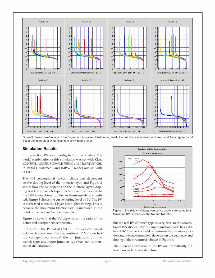
Figure 3. Breakdown Voltage of the Super Junction at each Nd doping level, the last IV curve shows the pin(red) and Trench(green) and Super Junction(blue) at Nd=Na=1e16 cm-3 doping level.
Figure 4. Breakdown Voltage versus Nd and Na concentations. Maximum BV depends on the Na and Nd ratio.
Simulation Results In this section, BV was investigated for the off-state. The model combination of this simulation was set with KLA, CONSRH, AUGER, FLDMOB FERMI and TRAP.TUNNEL in MODEL statement, and IMPACT model was set with SELB[7].
The PiN conventional junction diode was dependent on the doping level of the intrinsic layer, and Figure 2 shows how the BV depends on the intrinsic layer’s dop-ing level. The Trench type junction has results close to the PiN conventional diode, so those results are omit-ted. Figure 3 shows the curve doping level vs BV. The BV is decreased when the i layer has higher doping. This is because the maximum Electric Field is increased to the point of the avalanche phenomenon.
Figure 4 shows that the BV depends on the ratio of the donor and acceptor concentrations.
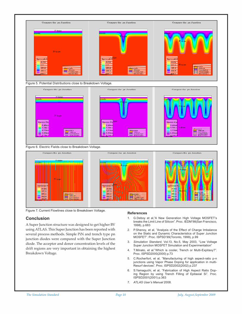
In Figure 5, the Potential Distribution was compared with each structure. The conventional PiN diode has the voltage drop around the on junctions but the trench type and super-junction type has two dimen-sional distributions.
But the real BV of trench type is very close to the conven-tional PiN diodes, only the super-junction diode has a dif-ferent BV. The Electric Field is minimized in the super junc-tion and the maximum field depends on the geometry and doping of the structure as shown in Figure 6.
The Current Flows around the BV are dramatically dif-ferent on each device structure.
The Simulation Standard Page 10 July, August,September 2009
Figure 5. Potential Distributions close to Breakdown Voltage.
Figure 6. Electric Fields close to Breakdown Voltage.
Figure 7. Current Flowlines close to Breakdown Voltage.
ConclusionA Super Junction structure was designed to get higher BV using ATLAS. This Super Junction has been reported with several process methods. Simple PiN and trench type pn junction diodes were compared with the Super Junction diode. The acceptor and donor concentration levels of the drift regions are very important in obtaining the highest Breakdown Voltage.
References1. G.Deboy et al,”A New Generation High Voltage MOSFET’s
breaks the Limit Line of Silicon”. Proc. IEDM’98(San Francisco, 1998), p.683
2. P.Shenoy, et al, ”Analysis of the Effect of Charge Imbalance on the Static and Dynamic Characteristics of Super Junction MOSFET”. Proc. ISPSD’99(Toronto, 1999), p.99
3. Simulation Standard, Vol.13, No.5, May 2003, “Low Voltage Super Junction MOSFET Simulation and Experimentation”
4. T.Minato, et al.”Which is cooler, Trench or Multi-Expitaxy?”. Proc. ISPSD2000(2000) p.73
5. C.Rocherfort, et al, ”Manufacturing of high aspect-ratio p-n junctions using Vapor Phase Doping for application in multi-Resurf devices”. Proc. ISPSD2002(2002) p.237
6. S.Yamaguchi, et al, ”Fabrication of High Aspect Ratio Dop-ing Region by using Trench Filling of Epitaxial Si”. Proc.ISPSD2001(2001) p.363
7. ATLAS User’s Manual 2008.