research article a novel sample based quadrature...
TRANSCRIPT

Research ArticleA Novel Sample Based Quadrature Phase Shift KeyingDemodulator
Asraf Mohamed Moubark and Sawal Hamid Md Ali
Department of Electrical, Electronic and Systems Engineering, Universiti Kebangsaan Malaysia, 43600 Bangi, Selangor, Malaysia
Correspondence should be addressed to Asraf Mohamed Moubark; [email protected]
Received 13 April 2014; Revised 21 July 2014; Accepted 22 July 2014; Published 14 August 2014
Academic Editor: Ramesh Pokharel
Copyright © 2014 A. Mohamed Moubark and S. H. M. Ali. This is an open access article distributed under the Creative CommonsAttribution License, which permits unrestricted use, distribution, and reproduction in any medium, provided the original work isproperly cited.
This paper presents a new practical QPSK receiver that uses digitized samples of incoming QPSK analog signal to determine thephase of the QPSK symbol. The proposed technique is more robust to phase noise and consumes up to 89.6% less power forsignal detection in demodulation operation. On the contrary, the conventional QPSK demodulation process where it uses coherentdetection technique requires the exact incoming signal frequency; thus, any variation in the frequency of the local oscillator orincoming signal will cause phase noise. A software simulation of the proposed design was successfully carried out using MATLABSimulink software platform. In the conventional system, at least 10 dB signal to noise ratio (SNR) is required to achieve the bit errorrate (BER) of 10−6, whereas, in the proposed technique, the same BER value can be achieved with only 5 dB SNR. Since some ofthe power consuming elements such as voltage control oscillator (VCO), mixer, and low pass filter (LPF) are no longer needed,the proposed QPSK demodulator will consume almost 68.8% to 99.6% less operational power compared to conventional QPSKdemodulator.
1. Introduction
Quadrature Phase Shift Keying (QPSK) is a modulationscheme commonly used in wireless communication systemdue to its ability to transmit twice the data rate for a givenbandwidth [1]. An ideal QPSK signal where the in-phaseand quadrature components are in quadrature (90∘) and haveequal amplitude cannot be obtained, according to [2] due tothe noise presence in local oscillator, DC offset in mixer, andphase imbalance in power combiner and mixers. At the sametime, the transmitted QPSK signal frequency, 𝜔
𝑐
, may alsovary byΔ𝜔 due toDoppler effect [3]. A practical QPSK signal,𝑠(𝑡), will contain gain error (𝜀), phase error (𝛽), and frequencyshift (Δ𝜔), as given in
𝑠 (𝑡) = (1 + 𝜀)√2Es𝑇
cos ((𝜔𝑐
+ Δ𝜔) 𝑡 + 𝜃 + 𝛽) , (1)
where fc is the carrier frequency, Es is the energy per symbol,𝑇 is the symbol period, and 𝜃 is the carrier phase. Whilethe gain error can be easily reduced with automatic gain
controller (AGC), the phase noise and frequency shift aremore complicated and can tremendously affect the perfor-mance of the system. The performance of a conventionalcoherent demodulator starts to degrade at phase noise of3.6∘ [4]. Previous works attempted to solve both phase errorand frequency shift problems by using feedback control loopand feed-forward compensation technique, only addingmorecomplexity to the demodulator circuit [5].
Typical QPSK demodulator needs SNR of 10 dB to pro-duce BER of 10−6 [1]. Even though the SNR value presumedas low in wireless signal transmission, for a system suchas satellite and mobile devices where their operations arepower limited, this is an issue that needs attention [6].Components used in the conventional QPSK demodulatorfor the demodulation process such as VCO, LPF, and mixersincrease the power consumption of the system. Thus, thispaper proposed a new technique that is simple, consumes lesspower, and is robust to the phase noise.
This paper is structured as follows. Section 1 gives anintroduction to readers about this journal. Section 2 briefly
Hindawi Publishing Corporatione Scientific World JournalVolume 2014, Article ID 107831, 7 pageshttp://dx.doi.org/10.1155/2014/107831

2 The Scientific World Journal
QPSK signal
ADC
++
++
++
+ +
−
−
− −
−
−
−−
0
0
0
0
1
1
11
4bits FIFO
8bits FIFO
4bits LUT 1
4bits LUT 2
4bits LUT 3
4bits LUT 4
4bits comparator 1
4bits comparator 2
4bits comparator 3
4bits comparator 4
2bit LUT 1
2bit LUT 2
2bit LUT 3
2bit LUT 4
Figure 1: Block diagram for the proposed 8S-QPSK demodulator.
explains the proposed new QPSK demodulator, followedby Section 3 showing MATLAB simulation carried out onthe proposed architecture. In Section 4 results obtained fromthe simulation are provided and discussed in detail. Finallyour results are concluded and some details about our futurework are given in Section 5.
2. Proposed QPSK Demodulator
The proposed QPSK demodulator uses polarity differencefrom digitized QPSK signal for the demodulation processand is given a new code name 8S-QPSK. Figure 1 shows thecomplete block diagram for the proposed design where itconsists of analog to digital converter (ADC), first in first out(FIFO), lookup table (LUT), and comparators.
Digitizing is a process used in ADC to convert the incom-ing analog signal to digital signal based on the ADC samplingrate. In the proposedQPSK demodulator the incoming signalis sampled 8 times of the incoming signal frequency. A sampleis produced for every rising clock of the ADC circuit fora total number of 8 samples. A decision is made on every2 samples to be classified as positive and negative samplesbased on the sample’s polarities. This will eventually produce4 different polarities for a QPSK signal and they are differentfor every QPSK symbol as shown in Table 1.
The QPSK phases represent a group of 2 bits data. Thephases are produced at modulation level according to theinputs bits to the sinusoidal carrier [7, 8]. Once the phasesare identified, the data can be recovered immediately.
3. MATLAB Simulation
The whole demodulation process starts with sampling ofthe QPSK signal from the signal recovery block by using
Table 1: Combinational polarities for QPSK symbols.
Phase Data 4 different polarities
45∘ 00 + − − +
135∘ 01 − − + +
225∘ 10 − + + −
315∘ 11 + + − −
the sample and hold circuit block.The sample and hold blockwill convert the continuous QPSK signal, 𝑠(𝑡), into discretesignal, 𝑆[𝑛], as given by
𝑆 [𝑛] =
𝑠 (𝑡)
𝑉𝑟
× 2𝑦
, (2)
where 𝑛 is the number of samples and 𝑦 is the quantizationlevel. The maximum range of the ADC voltage is ±𝑉
𝑟
centered on the reference voltage 0 v.The chosen transmittedcarrier frequency was 5MHz because it is a frequently usedbandwidth in wireless systems [9]. Therefore the samplingclock frequency used in sample and hold block was setto 8 times the incoming frequency which is 40MHz. Thesampling clock is set by using pulse generator where theperiod of the pulse can be programmed. A group, 𝑎
𝑘
{ }, of 8samples, 𝑆[𝑛], are produced for every phase of aQPSK symbolas given by
𝑎𝑘
{ } = 𝑆 [𝑛] , 𝑘 = 1 ⋅ ⋅ ⋅∞, 𝑛 = 1 ∼ 8. (3)
The Scientific World Journal 3
6 8 10 12 14 16
05
4−5
×10−7Time
(a)
6 8 10 12 14 164
1.5
−0.5
Time
0.5
×10−7
(b)
6 8 10 12 14 164
05
−5
Time ×10−7
(c)
02
−2
Time0.4 0.6 0.8 1 1.2 1.4 1.6
×10−6
(d)
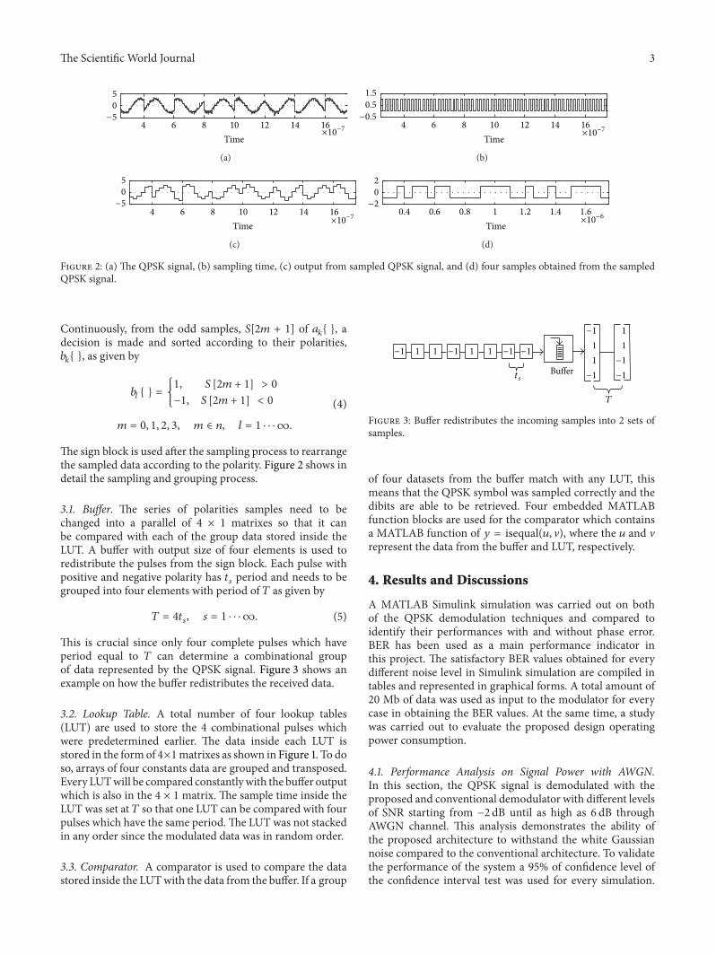
Figure 2: (a) The QPSK signal, (b) sampling time, (c) output from sampled QPSK signal, and (d) four samples obtained from the sampledQPSK signal.
Continuously, from the odd samples, 𝑆[2𝑚 + 1] of 𝑎𝑘
{ }, adecision is made and sorted according to their polarities,𝑏𝑘
{ }, as given by
𝑏𝑙
{ } = {
1, 𝑆 [2𝑚 + 1] > 0
−1, 𝑆 [2𝑚 + 1] < 0
𝑚 = 0, 1, 2, 3, 𝑚 ∈ 𝑛, 𝑙 = 1 ⋅ ⋅ ⋅∞.
(4)
The sign block is used after the sampling process to rearrangethe sampled data according to the polarity. Figure 2 shows indetail the sampling and grouping process.
3.1. Buffer. The series of polarities samples need to bechanged into a parallel of 4 × 1 matrixes so that it canbe compared with each of the group data stored inside theLUT. A buffer with output size of four elements is used toredistribute the pulses from the sign block. Each pulse withpositive and negative polarity has 𝑡
𝑠
period and needs to begrouped into four elements with period of 𝑇 as given by
𝑇 = 4𝑡𝑠
, 𝑠 = 1 ⋅ ⋅ ⋅∞. (5)
This is crucial since only four complete pulses which haveperiod equal to 𝑇 can determine a combinational groupof data represented by the QPSK signal. Figure 3 shows anexample on how the buffer redistributes the received data.
3.2. Lookup Table. A total number of four lookup tables(LUT) are used to store the 4 combinational pulses whichwere predetermined earlier. The data inside each LUT isstored in the formof 4×1matrixes as shown in Figure 1. To doso, arrays of four constants data are grouped and transposed.Every LUTwill be compared constantlywith the buffer outputwhich is also in the 4 × 1matrix. The sample time inside theLUT was set at 𝑇 so that one LUT can be compared with fourpulses which have the same period.The LUT was not stackedin any order since the modulated data was in random order.
3.3. Comparator. A comparator is used to compare the datastored inside the LUTwith the data from the buffer. If a group
−1
−1
−1
−1
−1−1−1 −1
1
11111
1
1
tsBuffer
T
Figure 3: Buffer redistributes the incoming samples into 2 sets ofsamples.
of four datasets from the buffer match with any LUT, thismeans that the QPSK symbol was sampled correctly and thedibits are able to be retrieved. Four embedded MATLABfunction blocks are used for the comparator which containsa MATLAB function of 𝑦 = isequal(𝑢, V), where the 𝑢 and Vrepresent the data from the buffer and LUT, respectively.
4. Results and Discussions
A MATLAB Simulink simulation was carried out on bothof the QPSK demodulation techniques and compared toidentify their performances with and without phase error.BER has been used as a main performance indicator inthis project. The satisfactory BER values obtained for everydifferent noise level in Simulink simulation are compiled intables and represented in graphical forms. A total amount of20 Mb of data was used as input to the modulator for everycase in obtaining the BER values. At the same time, a studywas carried out to evaluate the proposed design operatingpower consumption.
4.1. Performance Analysis on Signal Power with AWGN.In this section, the QPSK signal is demodulated with theproposed and conventional demodulator with different levelsof SNR starting from −2 dB until as high as 6 dB throughAWGN channel. This analysis demonstrates the ability ofthe proposed architecture to withstand the white Gaussiannoise compared to the conventional architecture. To validatethe performance of the system a 95% of confidence level ofthe confidence interval test was used for every simulation.

4 The Scientific World Journal
The confidence interval test was carried out by using MAT-LAB built-in function where it requires data such as BER,the total number of input data, and range of SNR to calculatethe interval level and the maximum and minimum numberof BER [10, 11]. The data compiled for both demodulationschemes are represented graphically in Figure 4. The expo-nential curve fit has been used to interpolate the log-log scaledataset so that the graph will resemble the water fall curveshape [12].
It can be seen from Figure 4, for a particular BER (e.g.,10−2), that the proposed technique has a lower SNR compared
to the conventional technique. The noise power, 𝑃noise, forboth signals can be determined using (6) and this noise powerwill be used together with the SNR value to give the signalpower, 𝑃signal, as depicted in (7). Table 2 shows the powercomparison for both techniques at BER of 10−2:
𝑃noise = (−173.83 + 10 log10
𝐵)dB𝑚 (6)
SNRdB = 10 log10
𝑃signal
𝑃noise. (7)
The result shows that, for a particular BER, the proposedmethod can reduce the signal detection power up to 74.9%when compared with conventional method and lower SNRvalues are obtained for every BER value. This is due to thearchitecture of the proposed design which no longer employscoherent detection technique in the demodulation process.
4.2. Performance Analysis on Signal Power with Phase Error.To determine the ability of the proposed design to toleratehigh phase error in AWGN channel, a simulation has beenperformed to obtained data for BER with respect to SNR for8S-QPSK and conventional QPSK schemes with phase errorsof 9∘, 18∘, and 27∘.The results obtained are shown in graphicalform in Figure 5. SNR values for BER of 10−2 are taken fromeach graph and shown inTable 3 for comparison. As for phaseerror of 18∘ and 27∘ for conventional QPSK schemes, the SNRvalues are only shown until 6 dB in Figure 6. However, theother two SNR values, 8 and 11.6 dB, have been successfullyobtained in the simulation conducted. In this simulation,confidence interval test is not included since the upper andlower limit values tend to overlap with each other betweenthe curves.
The proposed demodulator shows power gain of 5.2 dBfor 9∘ and 5.8 dB for 18∘ and 27∘ phase errors when comparedto conventional QPSK demodulator. This achievement isobtained because the samples used to identify the signalphase, 𝜃, are taken for every 45 degrees.Thus, if any variationhappened on the signal between the sampling period, it isnot going to affect the sample value obtained. As in Figure 6,the samples, 𝑆
1,2
[𝑛], represent ideal QPSK signal, 𝑆1
[𝑛], andphase error QPSK signal by 45 degrees, 𝑆
2
[𝑛]. As for bothsignals, samples obtained at any sampling time, 𝑛𝑇, give thesame positive or negative values regarding the phase error.The signals shown in Figure 6 are QPSK signals for 𝜃, 45∘
10−1
10−2
10−3
10−4
10−5
10−6
10−7
10−8
10−9
100
0 1 2 3 4 5 6SNR (dB)
BER
(dB)
−1−2
Empirical valueConfident interval
Exp fit for 8S-QPSKExp for con’v QPSK
BER versus SNR (dB) with exponential curve fit
Figure 4: Performance comparison of 8S-QPSK and conventionalQPSK scheme in additive white Gaussian noise (AWGN) channelwith confidence interval and empirical value.
0 1 2 3 4 5 6SNR (dB)
BER
(dB)
10−1
10−2
10−3
10−4
10−5
10−6−1−2
100
9deg 8S-QPSK9deg conventional QPSK
18deg conventional QPSK18deg 8S-QPSK
27deg 8S-QPSK27deg conventional QPSK
BER versus SNR for phase error of 9, 18, and 27 deg
Figure 5: Performance comparison of 8S-QPSK and conventionalQPSK signal with phase errors of 9∘, 18∘, and 27∘.

The Scientific World Journal 5
QPSK signal
Ideal QPSK signal
with phase error
T 2T 3T 4T 5T 6T 7T 8T
S1,2[1]
S1,2[2]
S1,2[3]
S1,2[4]
S1,2[5]
S1,2[6]
S1,2[7]
S1,2[8]
𝛽
Figure 6: Samples obtained for phase error and standard QPSKsignals from 𝑛 = 1 until 𝑛 = 8.
Table 2: Comparison of signal power between the two schemes.
Demodulationscheme
SNR for10𝐸−2 (dB)
Noise powerfor
6.75MHz(W)
Signalpower (W)
% ofpowersaved
ConventionalQPSK 5 2.78𝐸 − 14 8.79𝐸 − 14 0
8S-QPSK −1 2.78𝐸 − 14 2.20𝐸 − 14 74.9%
Table 3: Comparison of power gain between the 3 phases error atBER of 10−2.
Phaseerror
ConventionalQPSK(dB)
8S-QPSK(dB)
Power gain(dB)
9∘ 5.8 0.2 5.218∘ 8 2.2 5.827∘ 11.6 5.8 5.8
generated at high SNR value, and 10 dB to give an idea on howthe phase error alone will affect the sampling process:
𝑆1
[𝑛] = 𝑆2
[𝑛] =
2𝑚
√2 (cos (𝜔𝑐
𝑛𝑇 + 𝜃 + 𝛽1,2
))
𝑉𝑟
∈ {±1} ,
𝛽1
= 0∘
, 𝛽2
= 45∘
.
(8)
However, when SNR values for 8S-QPSK from Tables 3and 2 are compared, it shows that there are power incre-ments from 1.2 dB to 6.8 dB to obtain the same BER value.The degradation on the performance happened due to thedependency of the proposed design on the amplitude of theincoming signal. The white Gaussian noise will cause voltagefluctuation on the incoming signal and thus will cause thepolarity change in the sampling process. In conventional
method, the phase error with the presents of white noisecannot be corrected or rectified with high SNR value as inproposed method.
To demonstrate the phase error effect on conventionaldemodulator, gain error and frequency shift have beenremoved from the incoming QPSK signal as in (1) to easethe calculation. At the same time, the phase error only wasincluded into one of two local oscillators, sine carrier. This isto show clearly how phase error on one of the carriers cancause the demodulated data to be shifted in time domainwhen odd and even data were data merged together.
It can be seen that, by mixing the QPSK signal withthe sine carrier as shown in (9), it produces two differentterms. First, a sine signal with twice the frequency, phaseshifted and half amplitude from the incoming signal. Second,another sine signal which varies according to the phase errorand half the input amplitude signal. The first signal will besuperimposed on second signal which acts like dc offsetsignal. By using an LPF after themixing process, the first highfrequency term, 2𝜔
𝑐
, can be filtered out and the remainingterm given in the expression will cause the odd data to beshifted in time domain by Δ𝑡. Figure 7 shows output frommixing the QPSK and sine carrier, filtered I-channel signalwith LPF, and odd and even data obtained from I channeland Q-channel.The steps involved in obtaining the even dataare not shown here but they are the same as in (9). Theonly difference is the sine carrier substituted by cosine carrierwithout any phase error:
√2Es𝑇
cos (𝜔𝑐
𝑡 + 𝜃) × √2sin (𝜔𝑐
𝑡 + 𝛽)
= √2Es𝑇
[
𝑒𝑗(𝜔
𝑐𝑡+𝜃)
+ 𝑒−𝑗(𝜔
𝑐𝑡+𝜃)
2
×
𝑒𝑗(𝜔
𝑐𝑡+𝛽)
− 𝑒−𝑗(𝜔
𝑐𝑡+𝛽)
2𝑗
]
= √4Es𝑇
[
sin (2𝜔𝑐
𝑡 + 𝜃 + 𝛽)
2
−
sin (𝜃 − 𝛽)2
] .
(9)
It has been proven that a small variation (3.6∘) of phaseerror will seriously affect the demodulation process and causethe data to be misinterpreted. On the other hand, the newarchitecture uses polarity of samples to recognize the QPSKsignal symbols correctly and is not bounded with mixingsignal issue mentioned earlier.
4.3. Analysis of Power Consumption. Power consumptionestimation has been conducted for the proposed design basedon the power consumed by individual components obtainedfrom literature as shown in Table 4. For each one of thecomponents, maximum and a minimum values are takeninto consideration from various references so that it will givea rough idea for the total power consumption that can beexpected.
The number of components used in the simulation is asfollows: 1 unit of ADC, 16 units of 4×4 comparator, 8 units ofLUT, and 2 units of FIFO as shown in Figure 1. The following

6 The Scientific World Journal
Table 4: Power comparison for various components in QPSKdemodulator.
Components Researcher Power Speed
ADC [13] 0.732mW 1GSps[14] 62mW 1.4GSps
Comparator [15] 3.2 uW —[13] 36.25 uW —
LUT [16] 0.274 uW 2.98GHz[17] 26.452 uW —
FIFO [18] 1.39 uW —[19] 721 uW 2GHz
Even data Odd data
(a)
(b)
(c)Δt
Figure 7: (a) Output from mixer of QPSK and sine carrier, (b)filtered I-channel signal with LPF, and (c) showing the mismatch intime domain between even and odd data due to phase error in sinecarrier.
calculation shows the maximum and minimum power con-sumption for the proposed design:
𝑃8-QPSK (Min)
= 1 × 𝑃ADC + 16 × 𝑃comparator + 8 × 𝑃LUT + 2 × 𝑃FIFO
= 0.732mW + 16 (3.2 uW) + 8 (0.274 uW) + 2 (1.39 uW)
= 0.788mW
𝑃8-QPSK (Max)
= 1 × 𝑃ADC + 16 × 𝑃comparator + 8 × 𝑃LUT + 2 × 𝑃FIFO
= 62mW + 16 (36.25 uW) + 8 (26.452 uW) + 2 (721 uW)
= 64.233mW.
(10)
It can be seen that the power consumption of theproposed design is between 0.788mW and 64.233mWwhichis significantly reduced compared to the 206mW [20] con-sumed by the conventionalQPSK.The reduction of the powerconsumption is between 68.8 and 99.6%.
5. Conclusion and Future Work
A novel architecture for QPSK demodulator has beenproposed and demonstrated promising results. The resultsobtained for both demodulation schemes do not includeany error correction coding, phase, and frequency errordetection technique. The new demodulation technique usessamples polarity from ADC to identify the QPSK symbols.This indirectly eliminates the use of VCO, a component thatcontributes to the phase and frequency distortion. The newarchitecture consumes almost 74.9% less power for signaldetection in AWGN channel without any phase error and50 to 89.6% when phase error is presented. On top of that,the proposed design is also expected to consume 68.8 to99.6% less power and significant size reduction comparedwith conventional architecture.
As for future work, channel selection method, error cor-rection coding, and signal locking mechanism for samplingstarting timewill be included to further evaluate the proposedarchitecture. Hardware implementation on Virtex 6 FPGAboard has been planned for performance measurement andverification.
Conflict of Interests
The authors declare that there is no conflict of interestsregarding the publication of this paper.
References
[1] D. Roddy, Satellite Communications, McGraw Hill, New York,NY, USA, 4th edition, 2006.
[2] D. Master Easton, J. Snowdon, and D. Spencer, Quadraturephase error in receivers [Thesis of Science], University ofSouthampton, 2008.
[3] M. Sobol, “TheDoppler Effect and Digital Video Broadcasting,”17 pages, 2007, http://user.informatik.uni-goettingen.de/∼sem-inar/dvb/TheDopplerEffect V4 eng.pdf.
[4] K. Z. Chen and A. Q. Hu, “MPSK demodulation algorithmbased on pattern recognition,” in Proceedings of the 2008IEEE International Conference on Neural Networks & SignalProcessing, pp. 182–186, June 2008.
[5] Y. Liu and C. Tao, “Feedback compensation algorithm forBPSK/QPSK carrier synchronization,”Radioengineering, vol. 19,no. 1, pp. 149–154, 2010.
[6] T. S. Tuli, N. G. Orr, and R. E. Zee, “Low cost ground stationdesign for nanosatellite missions,” in Proceedings of the NorthAmerican Space Symposium, pp. 1–9, 2006.
[7] A.M.Moubark,M.A.M.Ali,H. Sanusi, S.M.Ali, andN.Zainal,“Simple QPSKmodulator implemented in virtex 6 FPGA boardfor satellite ground station,” in Proceeding of the InternationalConference on Computer Design, pp. 131–135, 2011.
[8] A. M. Moubark, M. A. Mohd Ali, H. Sanusi, and S. M. Ali,“FPGA implementation of low power digital QPSK modulatorusing verilogHDL,” Journal of Applied Sciences, vol. 13, no. 3, pp.385–392, 2013.
[9] R. Frank, “Evolution of air interface,” 2012, http://www.ieee-ottawa.ca/aicn/wpcontent/uploads/2012/05/Evolution-of-the-Air-Interface-v0.3.pdf.

The Scientific World Journal 7
[10] http://www.mathworks.com/help/comm/ug/bit-error-rate-ber.html#bsvziy0.
[11] Y. Fan, A versatile FPGA-based high speed bit error rate testingscheme [Master of Engineering], Department of Electrical andComputer Engineering McGill Univerity, Montreal, Canada,2003.
[12] C. Langton, “Intuitive Guide to Principles of Communications,”2002, http://complextoreal.com/wp-content/uploads/2013/01/linkbud.pdf.
[13] M. Subba Reddy and S. Tipu Rahaman, An Effective 6-bit FlashADC using Low Power CMOS Technology.
[14] R. Thirugnanam, D. S. Ha, and S. S. Choi, “Design of a 4-bit 1.4 GSamples/s low power folding ADC for DS-CDMAUWB transceivers,” in Proceedings of the IEEE InternationalConference on Ultra-Wideband (ICU ’05), pp. 536–541, Zurich,Switzerland, September 2005.
[15] M. F. Snoeij, A. J. P. Theuwissen, and J. H. Huijsing, “A 1.8 V3.2𝜇W Comparator for use in a CMOS imager column-levelsingle-slope ADC,” in Proceedings of the IEEE InternationalSymposium on Circuits and Systems (ISCAS ’05), pp. 6162–6165,May 2005.
[16] P. Velrajkumar, C. Senthilpari, G. Ramanamurthy, and E. K.Wong, “Proposed adder andmodified LUT bit parallel unrolledCORDIC circuit for an application in mobile robots,” AsianJournal of Scientific Research, vol. 6, no. 4, pp. 666–678, 2013.
[17] D. Kumar, P. Kumar, and M. Pattanaik, “Performance analysisof 90 nm Look up Table (LUT) for low power application,” inProceedings of the 13th Euromicro Conference on Digital SystemDesign, pp. 404–407, September 2010.
[18] M. Chang, P. Huang, andW. Hwang, “A robust ultra-low powerasynchronous FIFOmemory with self-adaptive power control,”in Proceedings of the IEEE International SOC Conference, pp.175–178, September 2008.
[19] M. E. S. Elrabaa, “A new FIFO design enabling fully-synchro-nous on-chip data communication network,” in Proceedingsof the Saudi International Electronics, Communications andPhotonics Conference (SIECPC ’11), pp. 1–6, Riyadh, SaudiArabia, April 2011.
[20] M. Chun, “BPSK, QPSK, 8-PSK Demodulator for FPGA 5pages,” http://www.innovative-dsp.com/support/datasheets/IP-PSK DEMOD4.pdf.

International Journal of
AerospaceEngineeringHindawi Publishing Corporationhttp://www.hindawi.com Volume 2014
RoboticsJournal of
Hindawi Publishing Corporationhttp://www.hindawi.com Volume 2014
Hindawi Publishing Corporationhttp://www.hindawi.com Volume 2014
Active and Passive Electronic Components
Control Scienceand Engineering
Journal of
Hindawi Publishing Corporationhttp://www.hindawi.com Volume 2014
International Journal of
RotatingMachinery
Hindawi Publishing Corporationhttp://www.hindawi.com Volume 2014
Hindawi Publishing Corporation http://www.hindawi.com
Journal ofEngineeringVolume 2014
Submit your manuscripts athttp://www.hindawi.com
VLSI Design
Hindawi Publishing Corporationhttp://www.hindawi.com Volume 2014
Hindawi Publishing Corporationhttp://www.hindawi.com Volume 2014
Shock and Vibration
Hindawi Publishing Corporationhttp://www.hindawi.com Volume 2014
Civil EngineeringAdvances in
Acoustics and VibrationAdvances in
Hindawi Publishing Corporationhttp://www.hindawi.com Volume 2014
Hindawi Publishing Corporationhttp://www.hindawi.com Volume 2014
Electrical and Computer Engineering
Journal of
Advances inOptoElectronics
Hindawi Publishing Corporation http://www.hindawi.com
Volume 2014
The Scientific World JournalHindawi Publishing Corporation http://www.hindawi.com Volume 2014
SensorsJournal of
Hindawi Publishing Corporationhttp://www.hindawi.com Volume 2014
Modelling & Simulation in EngineeringHindawi Publishing Corporation http://www.hindawi.com Volume 2014
Hindawi Publishing Corporationhttp://www.hindawi.com Volume 2014
Chemical EngineeringInternational Journal of Antennas and
Propagation
International Journal of
Hindawi Publishing Corporationhttp://www.hindawi.com Volume 2014
Hindawi Publishing Corporationhttp://www.hindawi.com Volume 2014
Navigation and Observation
International Journal of
Hindawi Publishing Corporationhttp://www.hindawi.com Volume 2014
DistributedSensor Networks
International Journal of