reliability report 56
TRANSCRIPT

RELIABILITY REPORT 56 2H 2013
2
Copyright © 2014 Altera Corporation. All rights reserved. Altera, The Programmable Solutions Company, the stylized Altera logo, specific device designations, and all other words and logos that are identified as trademarks and/or service marks are, unless noted otherwise, the trademarks and service marks of Altera Corporation in the U.S. and other countries. All other product or service names are the property of their respective holders. Altera products are protected under numerous U.S. and foreign patents and pending applications, maskwork rights, and copyrights. Altera warrants performance of its semiconductor products to current specifications in accordance with Altera's standard warranty, but reserves the right to make changes to any products and services at any time without notice. Altera assumes no responsibility or liability arising out of the application or use of any information, product, or service described herein except as expressly agreed to in writing by Altera Corporation. Altera customers are advised to obtain the latest version of device specifications before relying on any published information and before placing orders for products or services.
3
TABLE OF CONTENTS Overview .............................................................................................................................4
Altera Quality Policy .........................................................................................................4 Altera Quality Systems ......................................................................................................4
Figure 1: Typical Product Flow Chart ...................................................................................................... 5 Reliability Methodology ....................................................................................................6
Table I: Product Family Description ......................................................................................................... 6 Table II: Reliability Qualification Requirements....................................................................................... 8 Table III: Reliability Monitor Program...................................................................................................... 9
Lifetest: Methodology and Failure Rate Prediction .....................................................10 Lifetest Methodology............................................................................................................................... 10 Failure Rate Prediction ............................................................................................................................ 11 Table IV: Common Failure Mechanisms and Acceleration Factors ....................................................... 12
Lifetest Results .................................................................................................................13 Table V: Lifetest summary ..................................................................................................................... 13 FLEX 0.42 Products .............................................................................................................................. 14 FLEX 0.3/0.35 Products ........................................................................................................................ 15 FLEX, ACEX, and APEX 0.22 Products .............................................................................................. 16 APEX, Excalibur, and Mercury 0.18 Products ...................................................................................... 17 APEX and Mercury 0.15 Products ........................................................................................................ 18 Stratix, Stratix GX, Cyclone and HardCopy 0.13 Products................................................................... 19 Stratix II, Stratix II GX, Cyclone II, Arria GX and HardCopy II – 90 nm Products ............................... 20 Stratix III, Cyclone III and Cyclone IV – 65/60 nm Products ................................................................. 21 Stratix IV, Arria II GX & GZ and HardCopy III & IV – 40 nm Products ............................................... 22 Arria V and Cyclone V – 28nm Low Power Products ............................................................................. 23 Stratix V – 28nm High Performance Products ........................................................................................ 24 MAX 7000S and MAX 9000 – Third Generation ................................................................................... 25 MAX 7000A and MAX 3000A – Fourth Generation .............................................................................. 26 MAX 7000B – Fifth Generation .............................................................................................................. 27 MAX II, MAX V – 0.18 μm FLASH Products ....................................................................................... 28 Configuration Devices – EPROM ........................................................................................................... 29 Configuration Devices – Flash Memory .................................................................................................. 30 PowerSoC 5300 and 6300 Family ........................................................................................................... 31 PowerSoC EN2300 Family and EC2360 ................................................................................................. 32 PowerSoC EV1300 Family ...................................................................................................................... 33
High Temperature Storage .............................................................................................34 Reflow Simulation and Moisture Preconditioning .......................................................37 Accelerated Moisture Resistance ....................................................................................37
Autoclave ................................................................................................................................................. 37 Unbiased HAST ....................................................................................................................................... 37
Temperature Humidity Bias ...........................................................................................41 Highly Accelerated Stress Testing ........................................................................................................... 43
Temperature Cycling .......................................................................................................45 PowerSoC Device Package Stress ...................................................................................49 Temperature Humidity Test ...........................................................................................51
Solder Joint Reliability ....................................................................................................53 Serial Configuration Devices ..........................................................................................57
Quad-Serial Configuration Devices ...............................................................................57 0.15 μm process – Monitoring Results .................................................................................................... 57 0.11 μm process – Monitoring Results .................................................................................................... 58 65 nm process – Monitoring Results ....................................................................................................... 58

4
Overview
Altera® Corporation is the pioneer of programmable logic solutions, enabling system and semiconductor companies to rapidly and cost effectively innovate, differentiate, and win in their markets. Altera offers FPGAs, SoCs with embedded processor systems, and CPLDs in combination with software tools, intellectual property, embedded processors and customer support to provide high-value programmable solutions to over 16,000 customers worldwide.
Product information, such as device architecture, detailed packaging information, handling and surface mount guidelines, and product change notifications can be found at Altera's Web site: http://www.altera.com.
Altera Quality Policy Altera’s corporate mission is to be the preferred supplier of leading edge Programmable Logic Silicon Solutions, Custom Logic Products, Intellectual Property, related Software Development Tools, and Technical Support. Altera will use this advantage to gain market share penetration into the larger Logic IC market. To achieve and maintain this preferred supplier status, Altera must provide cost–effective, state–of–the–art solutions to our customers in a timely manner while consistently meeting or exceeding their quality, reliability, and service expectations.
The foundation of quality is individual effort. To achieve our goals, each Altera employee must produce quality work and conform to the appropriate procedures and specifications. Altera is committed to improving its quality management systems through established goals and review of its quality objectives.
Quality management is the responsibility of all Altera managers, directors, and officers. The management team must actively establish and maintain the management practices described in Altera’s Quality Manual.
Altera Quality Systems Altera has a closed-loop quality and reliability system that conforms to the requirements of ISO 9001:2008, MIL-I-45208 and JEDEC® standards. Altera and all of its major suppliers are ISO 9000 certified. Altera’s Reliability qualification and monitoring programs are also governed by internal specifications, which define procedures, pass/fail requirements, and corrective actions. Altera has been ISO9001 certified since October, 1994.
Altera is able to provide the automotive supply chain with the highest levels of quality and reliability because all of Altera’s foundry, assembly and test partners are certified and registered to the ISO/TS 16949 automotive industry quality standard.
Altera conducts automotive product qualification complying with AEC requirements from AECQ100 document at latest revision.
Altera performs comprehensive testing and manufacturing controls on all its products. Figure 1 shows a typical product manufacturing flow.

5
Figure 1: Typical Product Flow Chart
Wafer Inspection Visual and E-test, Sample 100% of all lots
Wafer Sort 1 DC Parametrics, Functionality Programmability, Non-Volatile Margin or SRAM Configuration
Data Retention Bake 245°C, 48 hours for all EPROM, EEPROM, and FLASH products
Wafer Sort 2 Margin Test EPROM, EEPROM, and FLASH (except MAX II & V) products
Assembly 2
nd, 3
rd, and 4
th Optical Sample Inspections, Inline
Mark
QA Electrical QA Electrical (SS=116, C=0)
Final Test AC and DC Parametrics, Functionality, Programmability or SRAM Configuration
Mark As Required
Visual Inspection Including machine inspection of all packages > 44 leads.
QA Inspection SS=116, C=0 Process/Paperwork Review
Inner Box and Transfer to Finished Goods Bake and Bag per Specification
Plant Clearance, Outer Box, and Ship
Wafer Fabrication All Critical Process Steps under SPC Control
6
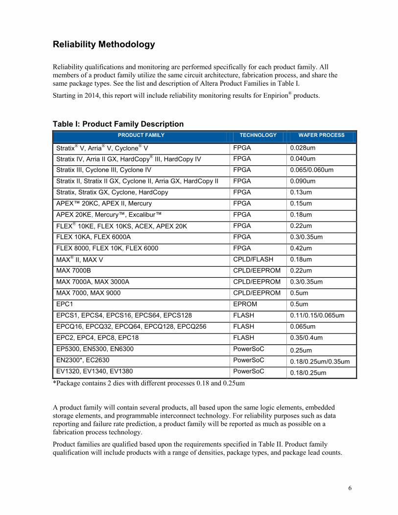
Reliability Methodology
Reliability qualifications and monitoring are performed specifically for each product family. All members of a product family utilize the same circuit architecture, fabrication process, and share the same package types. See the list and description of Altera Product Families in Table I.
Starting in 2014, this report will include reliability monitoring results for Enpirion® products.
Table I: Product Family Description PRODUCT FAMILY TECHNOLOGY WAFER PROCESS
Stratix® V, Arria® V, Cyclone® V FPGA 0.028um
Stratix IV, Arria II GX, HardCopy® III, HardCopy IV FPGA 0.040um
Stratix III, Cyclone III, Cyclone IV FPGA 0.065/0.060um
Stratix II, Stratix II GX, Cyclone II, Arria GX, HardCopy II FPGA 0.090um
Stratix, Stratix GX, Cyclone, HardCopy FPGA 0.13um
APEX™ 20KC, APEX II, Mercury FPGA 0.15um
APEX 20KE, Mercury™, Excalibur™ FPGA 0.18um
FLEX® 10KE, FLEX 10KS, ACEX, APEX 20K FPGA 0.22um
FLEX 10KA, FLEX 6000A FPGA 0.3/0.35um
FLEX 8000, FLEX 10K, FLEX 6000 FPGA 0.42um
MAX® II, MAX V CPLD/FLASH 0.18um
MAX 7000B CPLD/EEPROM 0.22um
MAX 7000A, MAX 3000A CPLD/EEPROM 0.3/0.35um
MAX 7000, MAX 9000 CPLD/EEPROM 0.5um
EPC1 EPROM 0.5um
EPCS1, EPCS4, EPCS16, EPCS64, EPCS128 FLASH 0.11/0.15/0.065um
EPCQ16, EPCQ32, EPCQ64, EPCQ128, EPCQ256 FLASH 0.065um
EPC2, EPC4, EPC8, EPC18 FLASH 0.35/0.4um
EP5300, EN5300, EN6300 PowerSoC 0.25um EN2300*, EC2630 PowerSoC 0.18/0.25um/0.35um EV1320, EV1340, EV1380 PowerSoC 0.18/0.25um
*Package contains 2 dies with different processes 0.18 and 0.25um
A product family will contain several products, all based upon the same logic elements, embedded storage elements, and programmable interconnect technology. For reliability purposes such as data reporting and failure rate prediction, a product family will be reported as much as possible on a fabrication process technology.
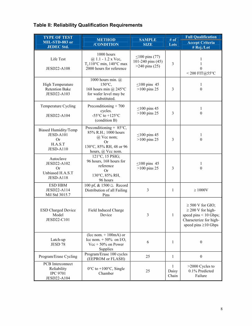
Product families are qualified based upon the requirements specified in Table II. Product family qualification will include products with a range of densities, package types, and package lead counts.

7
If a new product is added to the product family with a significant increase (more than 50%) in logic elements, a product qualification will be performed.
Reliability monitors are performed on a regular basis in order to assure that Altera’s normal production testing and process control methodologies produce reliable products. The reliability monitor program is also based upon a product family methodology. Different products and package types are procured from normal production on a Last in First out (LIFO) schedule to monitor product reliability. Results in this report cover data gathered at least in the last 36 months. For lifetest, the report covers a much larger period to assess FIT numbers more accurately.
Reliability monitor sampling is defined in Table III. Reliability monitor schedules depend on the maturity of the product: a minimum of 2 lots per year for mainstream products and 4 lots per year for new products. For mature and other products, if the volume from the current period is large enough to be statistically representative, Altera has a target of 1 lot per year.
Product category descriptions can be found in the Altera website earning reports.
All new results shown in this reliability report compared to previous version appear upfront in each table of results and are highlighted in a different color and font.
8
Table II: Reliability Qualification Requirements
TYPE OF TEST MIL-STD-883 or
JEDEC Std.
METHOD /CONDITION
SAMPLE SIZE
# of Lots
Full Qualification Accept Criteria
# Rej./Lot
Life Test
JESD22-A108
1000 hours @ 1.1 - 1.2 x Vcc,
Tj:110°C min, 140°C max 2000 hours for reference
<100 pins (77) 101-240 pins (45)
>240 pins (25)
3
1 1 0
< 200 FIT@55°C
High Temperature Retention Bake JESD22-A103
1000 hours min. @ 150°C,
168 hours min @ 245°C for wafer level may be
substituted.
<100 pins 45 >100 pins 25
3
1 0
Temperature Cycling
JESD22-A104
Preconditioning + 700 cycles.
-55°C to +125°C (condition B)
<100 pins 45 >100 pins 25
3
1 0
Biased Humidity/Temp JESD-A101
Or H.A.S.T
JESD-A110
Preconditioning + 85°C, 85% R.H.; 1000 hours
@ Vcc nom; Or
130°C, 85% RH, 48 or 96 hours, @ Vcc nom.
<100 pins 45 >100 pins 25
3
1 0
Autoclave JESD22-A102
Or Unbiased H.A.S.T
JESD-A118
121°C, 15 PSIG; 96 hours, 168 hours for
reference Or
130°C, 85% RH, 96 hours
<100 pins 45 >100 pins 25
3
1 0
ESD HBM JESD22-A114 Mil Std 3015.7
100 pf, & 1500 Ω. Record Distribution of all Failing
Pins 3 1 1000V
ESD Charged Device Model
JESD22-C101
Field Induced Charge Device
3 1
500 V for GIO; 200 V for high-
speed pins < 10 Gbps; Characterize for high-speed pins 10 Gbps
Latch-up JESD 78
(Icc nom. + 100mA) or Icc nom. + 50% on I/O,
Vcc + 50% on Power Supplies
6 1 0
Program/Erase Cycling Program/Erase 100 cycles (EEPROM or FLASH) 25 1 0
PCB Interconnect Reliability IPC 9701
JESD22-A104
0°C to +100°C, Single Chamber 25
1 Daisy Chain
>2000 Cycles to 0.1% Predicted
Failure

9
Table III: Reliability Monitor Program
TYPE OF TEST MIL-STD-883 or JEDEC
Std. METHOD/CONDITION SAMPLE
SIZE
Life Test
JESD22-A108
1000 hours @ 1.1 - 1.2 x Vcc nom. Tj :110°C min, 140°C max 2000 hours for reference
<100 pins 77pcs >100 -240 pins 45pcs
>240 pins 22pcs
High Temperature Retention Bake
Non-Volatile Products JESD22-A103
1000 hours min. @ 150°C
<100 pins 45pcs >100 pins 22pcs
Temperature Cycling
JESD22-A104
Preconditioning + 700 cycles. -55°C to +125°C Industrial, 0°C to +125°C Commercial,
<100 pins 45pcs >100 pins 22pcs
Biased Humidity/Temp. JESD-A101
Or H.A.S.T.
JESD-A110
Preconditioning + 85°C, 85% R.H. 1000 hours min. @ Vcc nominal;
Or 130°C, 85% RH,
96 hours, @ Vcc nominal
<100 pins 45pcs >100 pins 22pcs
Autoclave JESD22-A102
Or Unbiased H.A.S.T.
JESD-A118
121°C, 15 PSIG; 96 hours min. 168 hours for reference
Or 130°C, 85% RH,
96 hours
<100 pins 45pcs >100 pins 22pcs
Program/Erase Program/Erase 100 cycles (EEPROM or FLASH only) 22pcs

10
Lifetest: Methodology and Failure Rate Prediction
Lifetest Methodology Altera performs a high temperature / high voltage Lifetest on its products to accelerate failure mechanisms. Lifetest is conducted at a Junction Temperature of at least 125C and at a Vcc power supply increased by 10-20%. In some cases where increasing junction temperature to 125°C is not possible because of risk of thermal runaway, a minimum junction temperature of 110°C is used. The lifetest boards have special high temperature sockets that maintain lead integrity.
FLEX, APEX, Mercury, Stratix, Stratix GX, Cyclone, Stratix II, Stratix II GX, and Cyclone II devices use static life test mode. 65/60 nm, 40nm and 28 nm products use dynamic life with a real clocked configuration. MAX 3000, MAX 7000, MAX 9000 devices (EEPROM devices), MAX II and MAX V (FLASH devices) are first subjected to 100 Program Erase Cycles before starting Lifetest.
Each device is tested using production test equipment to data sheet specifications before being stressed. All readouts are also done on the same production test equipment to data sheet parameters. A device is considered a failure if it does not pass data sheet specifications.
For non-volatile configuration elements, except those on MAX II and V devices, there is a test mode that allows the configuration elements to be margin tested to determine the amount of charge on the floating gate. At each read-out, the margin of every configuration element is tested and the lowest margin is recorded. .

11
Failure Rate Prediction Altera uses exponential distribution of failures in time and predicts constant failure rate at operating conditions. Extrapolation uses thermal and voltage acceleration factor based on JEDEC formulas (JEP122).The formulas are presented below, and the acceleration factors are listed in Table IV.
Junction temperatures, not ambient temperatures, must be used in calculating thermal acceleration factors. A designer can determine device power dissipation using the Early Power Estimator (EPE) available on www.altera.com, or using the PowerPlay power analyzer in the Quartus II design tool. Junction temperatures are calculated from ambient temperature or case temperature measurements using the thermal resistance values found in the Altera Device Package Information Data Sheet. Thermal resistance values are specific to each product and package combination. For convenience, formulas to calculate junction temperatures are included with the acceleration formulas below.
Note also that temperatures must be converted to Degrees Kelvin when using the Temperature Acceleration formula below. Degrees Kelvin = Degrees Centigrade + 273.
Temperature Acceleration Factor = exp[Ea/((k)(Toperation)) - Ea/((k)(Tstress))]
k = Boltzmann’s constant = 8.62 x 10⁻⁵ eV/°K Ea = Activation energy in eV (see Table III) T = Junction Temperature in Degrees Kelvin kT(eV) = 0.0258 x (temperature in Centigrade + 273)/298
Gate Oxide Voltage Acceleration Factor = exp[(γ/(tox/10 nm))(Vstress - Voperation)]
γ = Voltage exponent factor (see Table III)
Interlayer Dielectric Acceleration Factor = exp[(γ)(Vstress - Voperation)]
Junction Temperature = (Ambient Temperature)+(Power dissipation)*(ja) = (Case Temperature)+(Power dissipation)*(jc)
ja and jc are found in the Altera Device Package Information Data Sheet.

12
Table IV: Common Failure Mechanisms and Acceleration Factors i
Mechanism Activation Energy “Ea” [eV] Voltage Exponent Factor
Gate Oxide Breakdown (≥ 90 nm)* 0.7 γ = 3.2 Interlayer defect 0.7 γ = 2.0
Via Voiding (0. 15 μm & 0. 13 μm) 0.8 0.0 Via Voiding (≤ 90 nm) 1.0 0.0 Silicon Junction Defect 0.8 0.0
Masking (Poly, Diffusion, etc.) Defect 0.5 0.0 Metallization Defect 0.5 0.0 Al Electromigration 0.7 (Al-Si), 0.85 (Al-Cu) Current density dependence (1/J2 )
Cu Electromigration (0. 13 μm, FSG dielectric)
0.8 Current density dependence (1/J2 )
Cu Electromigration (≤ 90 nm low-k dielectric)
0.9 Current density dependence (1/J )
Contamination (Surface & Bulk) 1.0 0.0 Data Retention
Charge Loss (EPROM) 0.6 0.0 Charge Detrapping (FLASH
&EEPROM, ≤ 168 hrs) 1.1 0.0
SILC (FLASH & EEPROM, > 168 hrs) 0 2.3
*≤ 65 nm process uses different values with power-law model
Failure rates are calculated on a product family basis (as in the tables of data on the following pages). Device hours accumulated at the stress conditions are converted to normal use conditions using the acceleration factors described above. Equivalent hours are calculated at a typical use condition of Vcc nominal in a 55°C still-air ambient or 70°C junction.
Failure rates are expressed in terms of FITs or Failures In Time, where one FIT is equivalent to one failure in one billion or 109 device-hours. Altera calculates the FIT rate using the JESD85 (Methods for Calculating Failure Rates in Units of FITs) standard.
The failure rate is calculated using a Chi-squared distribution to predict a 60% confidence level from the small number of failures and limited sample size of the population tested. The Chi-squared value is calculated from the inverse Chi-squared distribution using the desired probability level and the degrees of freedom. ii The degrees of freedom are calculated as: = 2n+2, where n= # of failures observed. The failure rate is then calculated from the Chi-squared value:
Failure Rate
A F Device hours
failureshour
2
2 . .
Device hours = (Hours in lifetest) x (Number of devices)
Acceleration Factor = (Thermal Acceleration) x (Voltage Acceleration)
The FIT rate is 109*Failure Rate and the Mean Time to Failure is simply the inverse of the failure rate for an exponential distribution.

13
Lifetest Results Lifetest results are summarized in table V. More details are presented on following pages.
Table V: Lifetest summary
PRODUCT FAMILY TECHNOLOGY NODE
DEVICE HOURS
@ STRESS CONDITIONS
NUMBER OF FAILS
FITs @
60% C.L.
Stratix V 0.028m 466,783 0 58.4 (1)
Arria V, Cyclone V 0.028m 1,038,341 0 26.6 (1) Stratix IV, Arria II GX, HardCopy III, HardCopy IV 0.040m 1,042,311 2 49.6 (1)
Stratix III, Cyclone III, Cyclone IV 0.065/0.060m 1,947,828 0 11.1 (1) Stratix II, Stratix II GX, Cyclone II, Arria GX, HardCopy II 0.090m 1,138,728 0 18.9 (1)
Stratix, Stratix GX, Cyclone, HardCopy 0.13m 1,489,590 0 5.5 (1)
APEX 20KC, APEX II, Mercury 0.15m 125,000 0 3.9 (1)
APEX 20KE, Mercury, Excalibur 0.18m 285575 0 48.4 (2)
FLEX 10KE, FLEX 10KS, ACEX, APEX 20K 0.22m 535,000 0 5.1 (2)
FLEX 10KA, FLEX 6000A 0.3/0.35m 330,000 0 53.7 (2)
FLEX 8000, FLEX 10K, FLEX 6000 0.42m 350,660 0 22.0 (2)
MAX II, MAX V 0.18m 2,084,000 0 11.3 (1)
MAX 7000B 0.22m 125,000 0 36.0 (1)
MAX 7000A, MAX 3000A 0.3/0.35m 1,199,000 0 7.9 (1)
MAX 7000S, MAX 9000 0.5m 466,235 0 22.1 (1)
EPC1 0.5m 616,000 0 31.3 (2)
EPC2, EPC4, EPC8, EPC18 0.35 /0.4m 800,000 0 5.7 (2)
EPCS1 0.11m 350,000 0 1 (2)
EPCS4, EPCS16, EPCS64 0.15m 263,000 0 1 (2) EPCS128, EPCQ16, EPCQ32, EPCQ64. EPCQ128, EPCQ256 0.065m 343,000 0 4 (2)
EP5300, EN5300, EN6300 (5V,6V) 0.25um 3,033,000 0 2.2 (1)
EN2300, EC2630 (12V) 0.18/0.25m/0.35um 159,000 0 3.1 (1)
EV1320, EV1340, EV1380 (1.8V) 0.18/0.25m 160,000 0 45.8 (1)
(1) FITs calculated at 70C junction operating temperature (2) FITs calculated at 55C ambient operating temperature
14
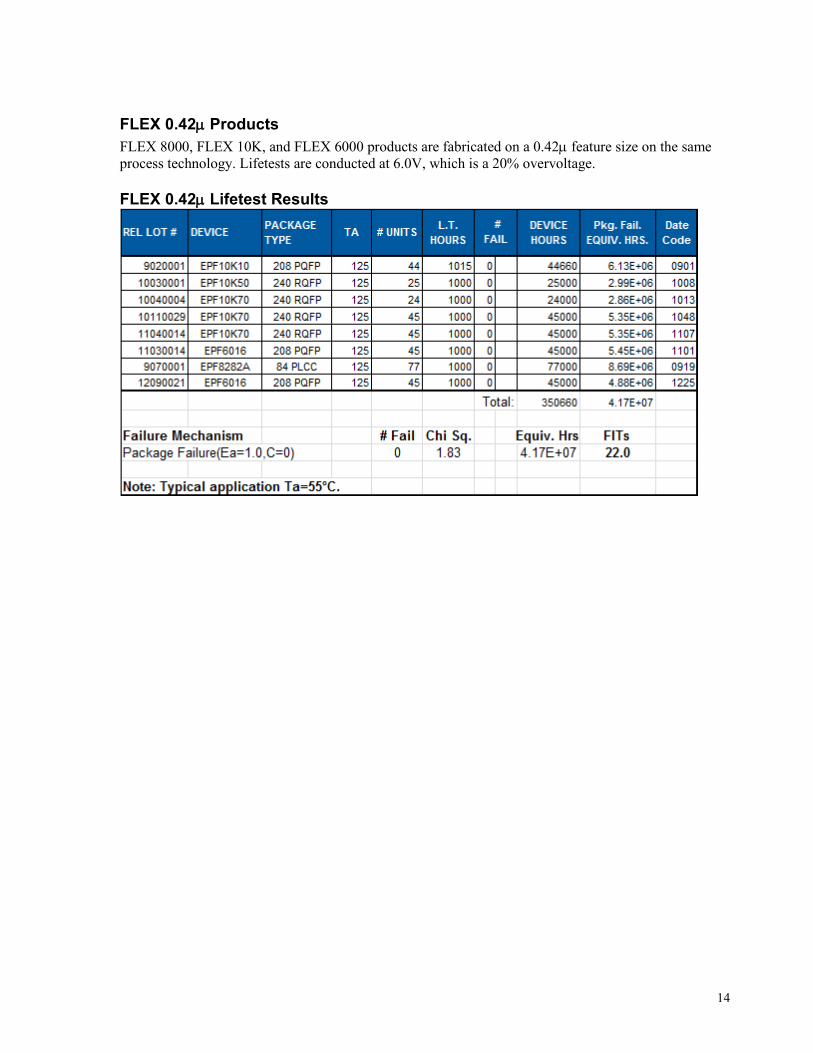
FLEX 0.42 Products FLEX 8000, FLEX 10K, and FLEX 6000 products are fabricated on a 0.42 feature size on the same process technology. Lifetests are conducted at 6.0V, which is a 20% overvoltage. FLEX 0.42 Lifetest Results

15
FLEX 0.3/0.35 Products FLEX 10KA and FLEX 6000A products are fabricated on a 0.3/0.35 process technology. Devices are available in TQFP, PQFP, RQFP, FBGA and BGA packages. The process technology operates with a 3.3V supply voltage and has I/Os that are 2.5V and 5.0V tolerant. Lifetests are conducted at 4.0V, which is a 20% overvoltage. FLEX 0.3/0.35 Lifetest Results
16
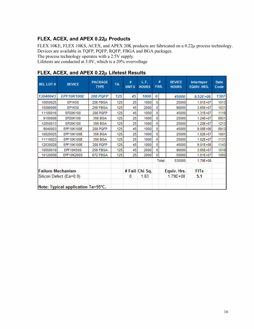
FLEX, ACEX, and APEX 0.22 Products FLEX 10KE, FLEX 10KS, ACEX, and APEX 20K products are fabricated on a 0.22 process technology. Devices are available in TQFP, PQFP, RQFP, FBGA and BGA packages. The process technology operates with a 2.5V supply. Lifetests are conducted at 3.0V, which is a 20% overvoltage FLEX, ACEX, and APEX 0.22 Lifetest Results
17
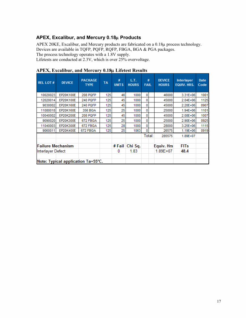
APEX, Excalibur, and Mercury 0.18 Products APEX 20KE, Excalibur, and Mercury products are fabricated on a 0.18 process technology. Devices are available in TQFP, PQFP, RQFP, FBGA, BGA & PGA packages. The process technology operates with a 1.8V supply. Lifetests are conducted at 2.3V, which is over 25% overvoltage. APEX, Excalibur, and Mercury 0.18 Lifetest Results
18
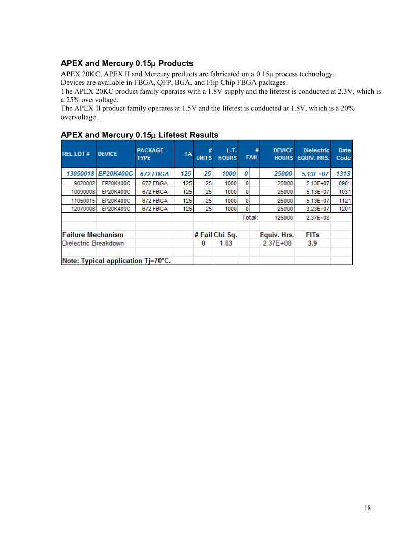
APEX and Mercury 0.15 Products APEX 20KC, APEX II and Mercury products are fabricated on a 0.15µ process technology. Devices are available in FBGA, QFP, BGA, and Flip Chip FBGA packages. The APEX 20KC product family operates with a 1.8V supply and the lifetest is conducted at 2.3V, which is a 25% overvoltage. The APEX II product family operates at 1.5V and the lifetest is conducted at 1.8V, which is a 20% overvoltage.. APEX and Mercury 0.15 Lifetest Results

19
Stratix, Stratix GX, Cyclone and HardCopy 0.13 Products Stratix, Stratix GX, Cyclone and HardCopy products are fabricated on a 0.13µ process technology. Devices are available in FBGA, QFP, BGA, and FlipChip FBGA packages. The Stratix, Stratix GX, Cyclone and HardCopy product families operate with a 1.5V supply. The lifetest is conducted at 1.8V, which is a 20% overvoltage. A lifetest temperature of 100°C is used on some devices to keep junction temperature below absolute maximum ratings. Stratix, Stratix GX, Cyclone and HardCopy 0.13 Lifetest Results

20
Stratix II, Stratix II GX, Cyclone II, Arria GX and HardCopy II – 90 nm Products Stratix II, Stratix II GX, Cyclone II, Arria GX and HardCopy II products are fabricated on a 90 nm process technology. Stratix II and GX devices are available in FlipChip FBGA packages. Cyclone II devices are available in QFP, FBGA and UBGA packages. The Stratix II, Stratix II GX, Cyclone II, Arria GX and HardCopy II product families operate with a 1.2V supply and the lifetest is conducted at 1.44V, which is a 20% overvoltage Lifetest is run at junction temperature of 125°C to keep it below absolute maximum ratings. Stratix II, Stratix II GX, Cyclone II, Arria GX and HardCopy II – 90 nm Lifetest Results

21
Stratix III, Cyclone III and Cyclone IV – 65/60 nm Products Stratix III, Cyclone III and Cyclone IV products are fabricated on a 65/60 nm process technology. Stratix III devices are available in FlipChip FBGA packages. Cyclone III and Cyclone IV devices are available in QFP, QFN, FBGA and UBGA packages. The Stratix III product families operate with a 1.1V supply. Lifetest is conducted at 1.32V The Cyclone III and Cyclone IV product families operate with a 1.2V supply. Lifetest is conducted at 1.44V. Stratix III, Cyclone III and Cyclone IV – 65/60 nm Lifetest

22
Stratix IV, Arria II GX & GZ and HardCopy III & IV – 40 nm Products Stratix IV, Arria II GX and HardCopy III & IV products are fabricated on a 40 nm process technology Stratix IV and Arria II GX devices are available in FlipChip FBGA packages. The Stratix IV, Arria II GX and HardCopy III & IV product families operate with a 0.9 V supply. Stratix IV lifetest is conducted at 1.1 x Vcc while Arria II and HardCopy III & IV lifetest is conducted at 1.2 x Vcc Stratix IV, Arria II GX and HardCopy III & IV – 40 nm Lifetest
23
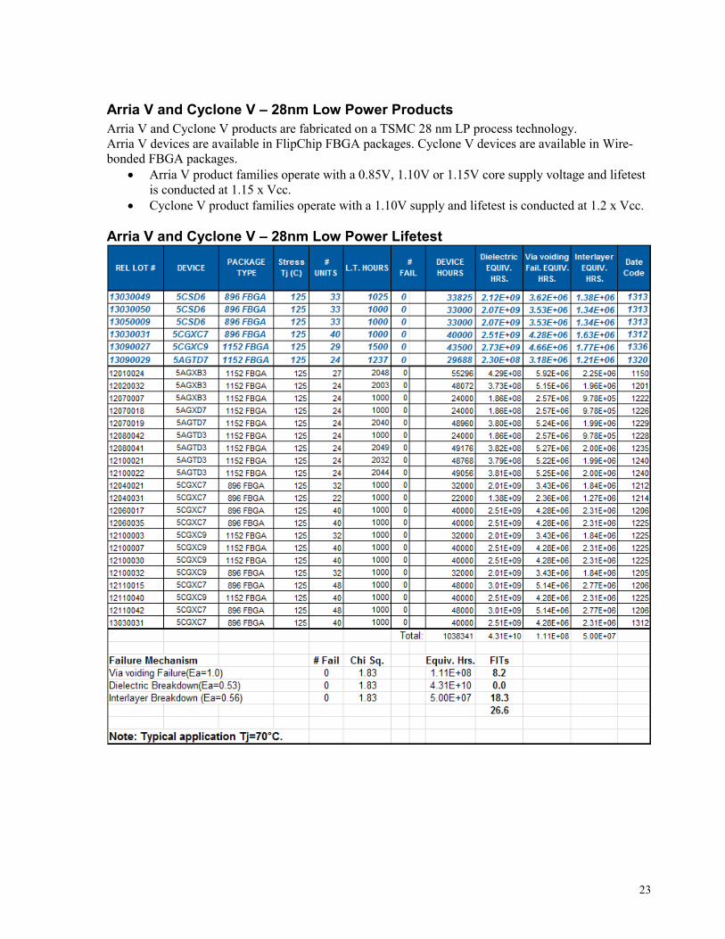
Arria V and Cyclone V – 28nm Low Power Products Arria V and Cyclone V products are fabricated on a TSMC 28 nm LP process technology. Arria V devices are available in FlipChip FBGA packages. Cyclone V devices are available in Wire-bonded FBGA packages.
Arria V product families operate with a 0.85V, 1.10V or 1.15V core supply voltage and lifetest is conducted at 1.15 x Vcc.
Cyclone V product families operate with a 1.10V supply and lifetest is conducted at 1.2 x Vcc. Arria V and Cyclone V – 28nm Low Power Lifetest
24
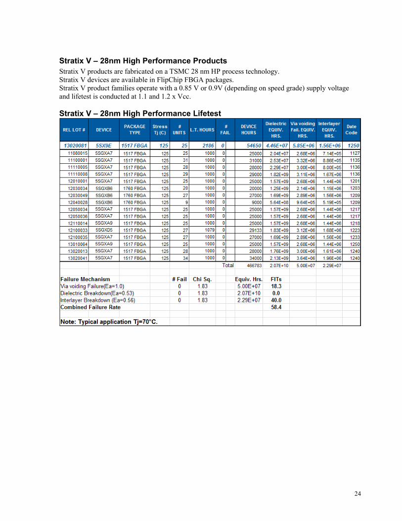
Stratix V – 28nm High Performance Products Stratix V products are fabricated on a TSMC 28 nm HP process technology. Stratix V devices are available in FlipChip FBGA packages. Stratix V product families operate with a 0.85 V or 0.9V (depending on speed grade) supply voltage and lifetest is conducted at 1.1 and 1.2 x Vcc. Stratix V – 28nm High Performance Lifetest
25
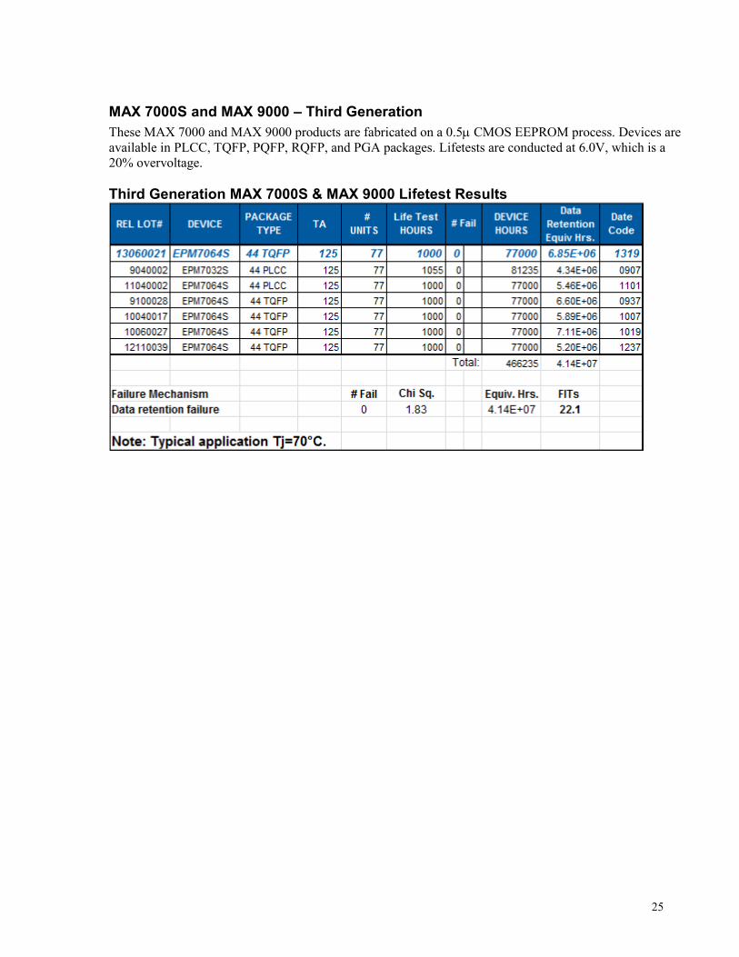
MAX 7000S and MAX 9000 – Third Generation These MAX 7000 and MAX 9000 products are fabricated on a 0.5 CMOS EEPROM process. Devices are available in PLCC, TQFP, PQFP, RQFP, and PGA packages. Lifetests are conducted at 6.0V, which is a 20% overvoltage. Third Generation MAX 7000S & MAX 9000 Lifetest Results
26
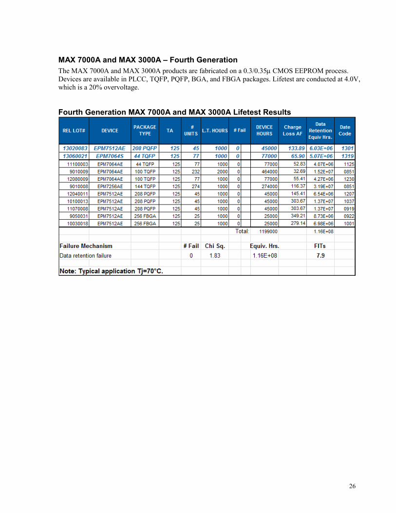
MAX 7000A and MAX 3000A – Fourth Generation The MAX 7000A and MAX 3000A products are fabricated on a 0.3/0.35 CMOS EEPROM process. Devices are available in PLCC, TQFP, PQFP, BGA, and FBGA packages. Lifetest are conducted at 4.0V, which is a 20% overvoltage. Fourth Generation MAX 7000A and MAX 3000A Lifetest Results
27
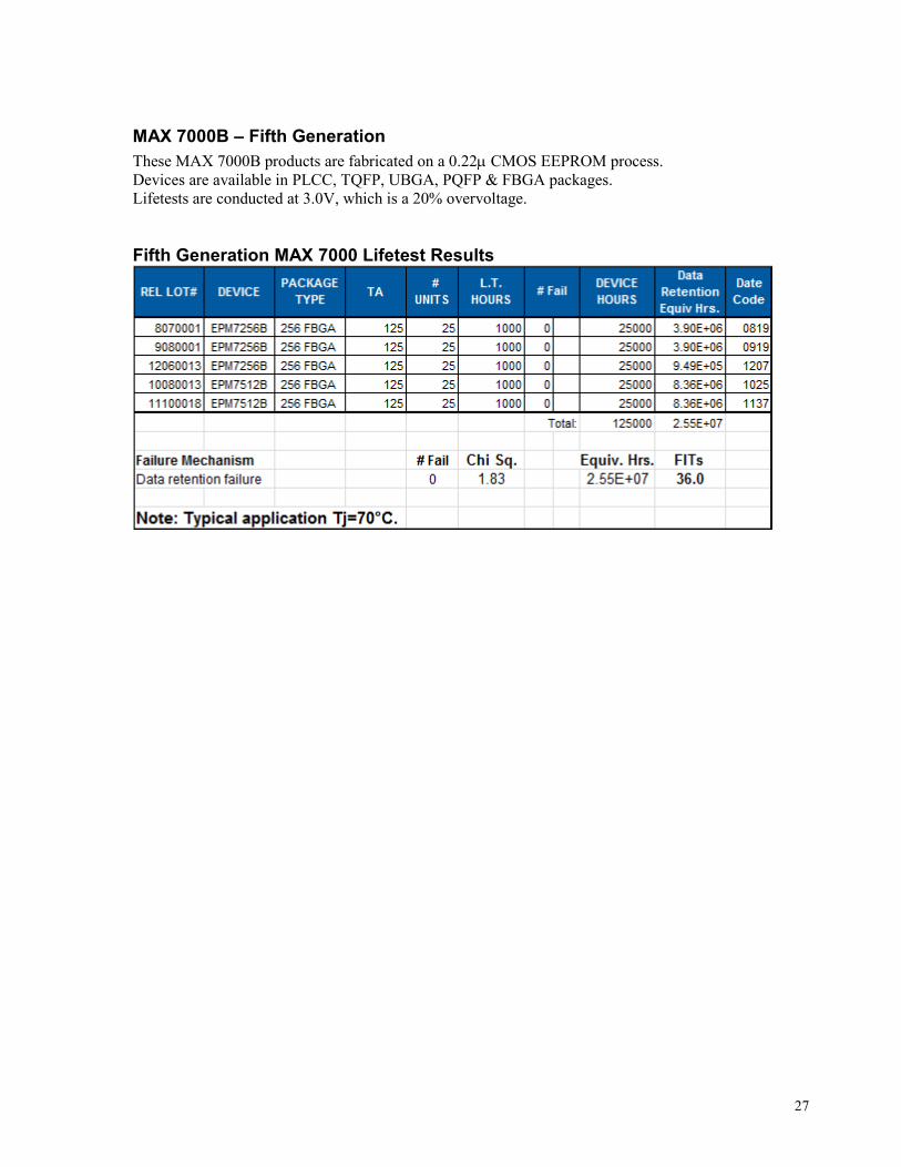
MAX 7000B – Fifth Generation These MAX 7000B products are fabricated on a 0.22 CMOS EEPROM process. Devices are available in PLCC, TQFP, UBGA, PQFP & FBGA packages. Lifetests are conducted at 3.0V, which is a 20% overvoltage. Fifth Generation MAX 7000 Lifetest Results
28
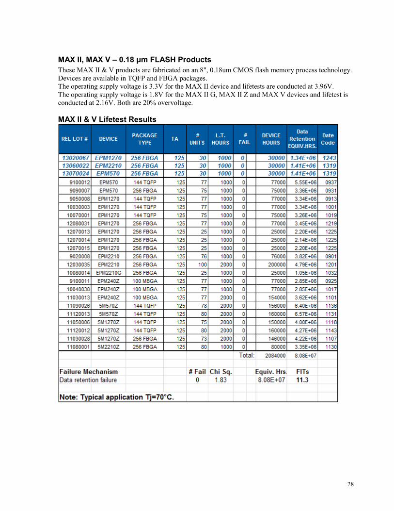
MAX II, MAX V – 0.18 μm FLASH Products These MAX II & V products are fabricated on an 8", 0.18um CMOS flash memory process technology. Devices are available in TQFP and FBGA packages. The operating supply voltage is 3.3V for the MAX II device and lifetests are conducted at 3.96V. The operating supply voltage is 1.8V for the MAX II G, MAX II Z and MAX V devices and lifetest is conducted at 2.16V. Both are 20% overvoltage. MAX II & V Lifetest Results

29
Configuration Devices – EPROM These Configuration EPROMs are fabricated on a 0.5m CMOS EPROM process. These devices are erasable with UV light when supplied in windowed hermetic packages for prototyping. Lifetests are conducted at least 6.0V, which is a minimum of 20% overvoltage. Third Generation Classic and Configuration Devices Lifetest Results

30
Configuration Devices – Flash Memory The EPC2 configuration device is fabricated on a 0.4 CMOS Flash process. EPC4, EPC8 and EPC16 are stacked-die configuration devices in which the controller die is fabricated on a 0.35 double layer metal CMOS logic process and the memory die is fabricated on 0.13 triple layer metal CMOS Flash process. These devices are electrically erasable. Lifetests are conducted at least at 6.0V and 4.0V for EPC2 and EPC16 respectively, which is a minimum of 20% overvoltage. Flash Memory Devices Lifetest Results
31
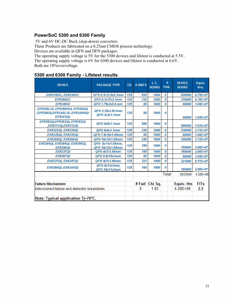
PowerSoC 5300 and 6300 Family 5V and 6V DC-DC Buck (step-down) converters These Products are fabricated on a 0.25um CMOS process technology. Devices are available in QFN and DFN packages. The operating supply voltage is 5V for the 5300 devices and lifetest is conducted at 5.5V. The operating supply voltage is 6V for 6300 devices and lifetest is conducted at 6.6V. Both are 10%overvoltage.
5300 and 6300 Family - Lifetest results

32
PowerSoC EN2300 Family and EC2360 12V DC-DC Buck (step-down) and Bus Converters EN2300 Products are made of 2 dies inserted in QFN packages. One die is fabricated on a 0.18um CMOS technology, the other die is fabricated on a 0.25um CMOS technology. The operating supply voltage is 12V and lifetest is conducted at 13.2V. EN2300 Family, EC2360 - Lifetest results
33
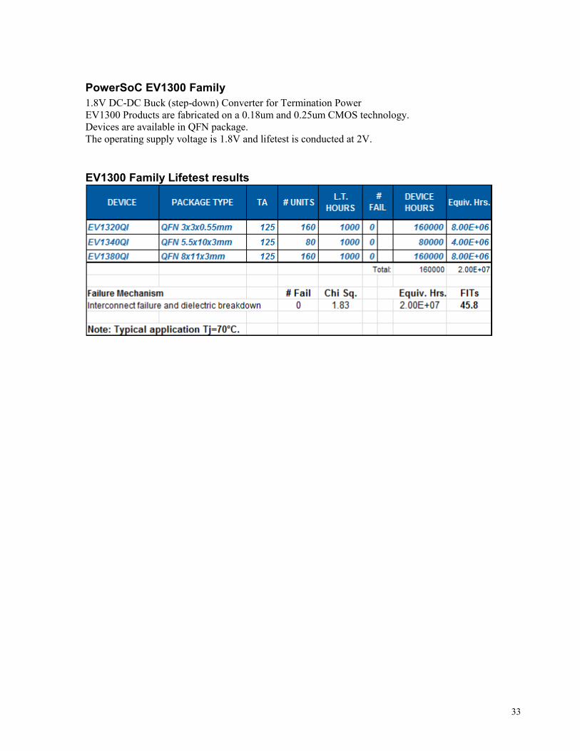
PowerSoC EV1300 Family 1.8V DC-DC Buck (step-down) Converter for Termination Power EV1300 Products are fabricated on a 0.18um and 0.25um CMOS technology. Devices are available in QFN package. The operating supply voltage is 1.8V and lifetest is conducted at 2V. EV1300 Family Lifetest results
34
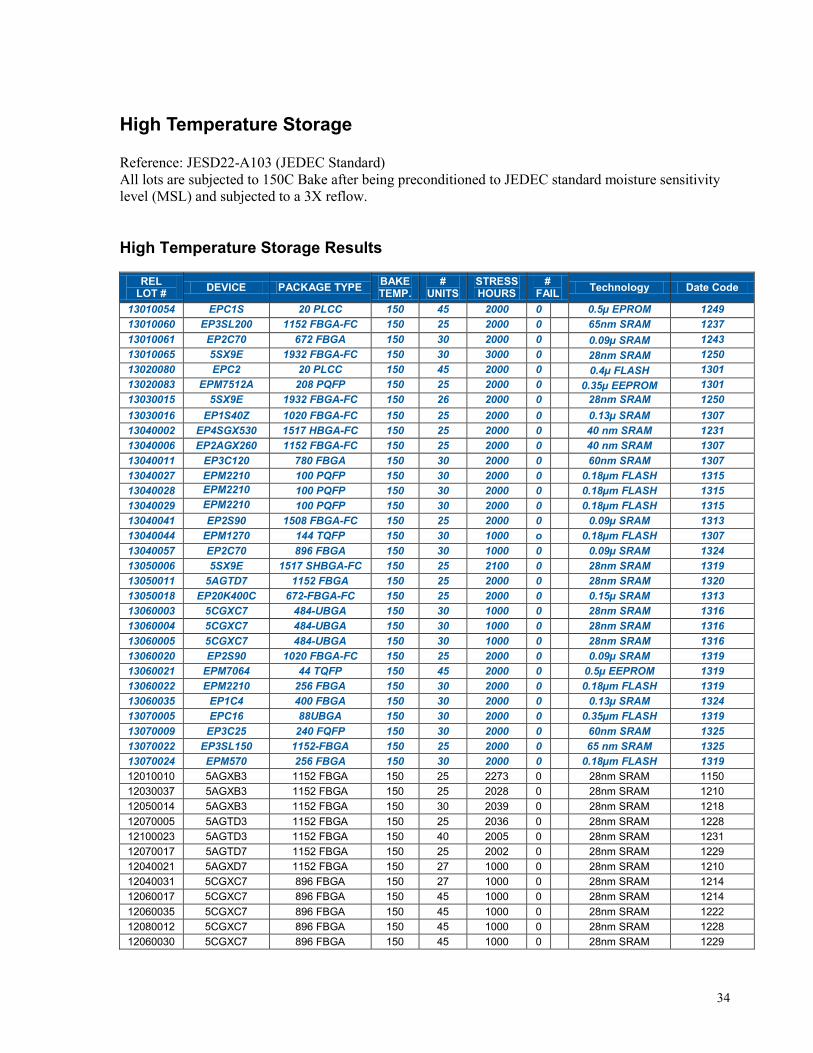
High Temperature Storage Reference: JESD22-A103 (JEDEC Standard) All lots are subjected to 150C Bake after being preconditioned to JEDEC standard moisture sensitivity level (MSL) and subjected to a 3X reflow. High Temperature Storage Results
REL
LOT # DEVICE PACKAGE TYPE BAKE TEMP.
# UNITS
STRESS HOURS
# FAIL Technology Date Code
13010054 EPC1S 20 PLCC 150 45 2000 0 0.5µ EPROM 1249 13010060 EP3SL200 1152 FBGA-FC 150 25 2000 0 65nm SRAM 1237 13010061 EP2C70 672 FBGA 150 30 2000 0 0.09µ SRAM 1243 13010065 5SX9E 1932 FBGA-FC 150 30 3000 0 28nm SRAM 1250 13020080 EPC2 20 PLCC 150 45 2000 0 0.4µ FLASH 1301 13020083 EPM7512A 208 PQFP 150 25 2000 0 0.35µ EEPROM 1301 13030015 5SX9E 1932 FBGA-FC 150 26 2000 0 28nm SRAM 1250 13030016 EP1S40Z 1020 FBGA-FC 150 25 2000 0 0.13µ SRAM 1307 13040002 EP4SGX530 1517 HBGA-FC 150 25 2000 0 40 nm SRAM 1231 13040006 EP2AGX260 1152 FBGA-FC 150 25 2000 0 40 nm SRAM 1307 13040011 EP3C120 780 FBGA 150 30 2000 0 60nm SRAM 1307 13040027 EPM2210 100 PQFP 150 30 2000 0 0.18µm FLASH 1315 13040028 EPM2210 100 PQFP 150 30 2000 0 0.18µm FLASH 1315 13040029 EPM2210 100 PQFP 150 30 2000 0 0.18µm FLASH 1315 13040041 EP2S90 1508 FBGA-FC 150 25 2000 0 0.09µ SRAM 1313 13040044 EPM1270 144 TQFP 150 30 1000 o 0.18µm FLASH 1307 13040057 EP2C70 896 FBGA 150 30 1000 0 0.09µ SRAM 1324 13050006 5SX9E 1517 SHBGA-FC 150 25 2100 0 28nm SRAM 1319 13050011 5AGTD7 1152 FBGA 150 25 2000 0 28nm SRAM 1320 13050018 EP20K400C 672-FBGA-FC 150 25 2000 0 0.15µ SRAM 1313 13060003 5CGXC7 484-UBGA 150 30 1000 0 28nm SRAM 1316 13060004 5CGXC7 484-UBGA 150 30 1000 0 28nm SRAM 1316 13060005 5CGXC7 484-UBGA 150 30 1000 0 28nm SRAM 1316 13060020 EP2S90 1020 FBGA-FC 150 25 2000 0 0.09µ SRAM 1319 13060021 EPM7064 44 TQFP 150 45 2000 0 0.5µ EEPROM 1319 13060022 EPM2210 256 FBGA 150 30 2000 0 0.18µm FLASH 1319 13060035 EP1C4 400 FBGA 150 30 2000 0 0.13µ SRAM 1324 13070005 EPC16 88UBGA 150 30 2000 0 0.35µm FLASH 1319 13070009 EP3C25 240 FQFP 150 30 2000 0 60nm SRAM 1325 13070022 EP3SL150 1152-FBGA 150 25 2000 0 65 nm SRAM 1325 13070024 EPM570 256 FBGA 150 30 2000 0 0.18µm FLASH 1319 12010010 5AGXB3 1152 FBGA 150 25 2273 0 28nm SRAM 1150 12030037 5AGXB3 1152 FBGA 150 25 2028 0 28nm SRAM 1210 12050014 5AGXB3 1152 FBGA 150 30 2039 0 28nm SRAM 1218 12070005 5AGTD3 1152 FBGA 150 25 2036 0 28nm SRAM 1228 12100023 5AGTD3 1152 FBGA 150 40 2005 0 28nm SRAM 1231 12070017 5AGTD7 1152 FBGA 150 25 2002 0 28nm SRAM 1229 12040021 5AGXD7 1152 FBGA 150 27 1000 0 28nm SRAM 1210 12040031 5CGXC7 896 FBGA 150 27 1000 0 28nm SRAM 1214 12060017 5CGXC7 896 FBGA 150 45 1000 0 28nm SRAM 1214 12060035 5CGXC7 896 FBGA 150 45 1000 0 28nm SRAM 1222 12080012 5CGXC7 896 FBGA 150 45 1000 0 28nm SRAM 1228 12060030 5CGXC7 896 FBGA 150 45 1000 0 28nm SRAM 1229

35
REL LOT # DEVICE PACKAGE TYPE BAKE
TEMP. #
UNITS STRESS HOURS
# FAIL Technology Date Code
12100003 5CGXC9 1152 FBGA 150 30 1000 0 28nm SRAM 1225 12100027 5CGXC7 896 FBGA 150 45 1000 0 28nm SRAM 1206 12100030 5CGXC9 1152 FBGA 150 30 1000 0 28nm SRAM 1225 12110040 5CGXC9 1152 FBGA 150 45 1000 0 28nm SRAM 1225 12110042 5CGXC7 896 FBGA 150 30 1000 0 28nm SRAM 1206 11120013 5M570Z 144 TQFP 150 102 2000 0 0.18µ FLASH 1131 11090026 5M570Z 144 FBGA 150 102 2000 0 0.18µ FLASH 1136 11050006 5M1270Z 144 TQFP 150 102 2000 0 0.18µ FLASH 1118 11120012 5M1270Z 144 TQFP 150 102 2000 0 0.18µ FLASH 1143 11030028 5M1270Z 256 FBGA 150 102 1000 0 0.18µ FLASH 1107 11050011 5M1270Z 256 FBGA 150 37 2000 0 0.18µ FLASH 1118 11080001 5M2210Z 256 FBGA 150 102 2000 0 0.18µ FLASH 1130 11080020 5M2210Z 256 FBGA 150 30 2001 0 0.18µ FLASH 1134 11080021 5M2210Z 256 FBGA 150 30 2001 0 0.18µ FLASH 1134 11080022 5M2210Z 256 FBGA 150 29 2001 0 0.18µ FLASH 1134 12010017 5M2210Z 256 FBGA 150 77 2000 0 0.18µ FLASH 1201 12100034 5SGSD5 1517 FBGA 150 26 2360 0 28 nm SRAM 1223 11100001 5SGXA7 1517 FBGA 150 29 2983 0 28 nm SRAM 1135 11110002 5SGXA7 1517 FBGA 150 29 2697 0 28 nm SRAM 1136 11110009 5SGXA7 1517 FBGA 150 30 2086 0 28 nm SRAM 1136 11080016 5SGXA7 1517 FBGA 150 27 1042 0 28 nm SRAM 1127 11110006 5SGXA7 1517 FBGA 150 30 2675 0 28 nm SRAM 1136 12110013 5SGXA9 1932 FBGA 150 30 2006 0 28 nm SRAM 1241 12030046 5SGXB6 1760 FBGA 150 28 2197 0 28 nm SRAM 1209 12050025 5SGXA7 1517 FBGA 150 25 2063 0 28 nm SRAM 1712 11060013 EP1C3 144 TQFP 150 77 1000 0 0.13µ SRAM 1137 12040014 EP1C4 400 FBGA 150 77 2000 0 0.13µ SRAM 1204 11110022 EP1C20 324 FBGA 150 77 2000 0 0.13µ SRAM 1119 11030011 EP1S40 1508 FBGA 150 25 1000 0 0.13µ SRAM 1001 12010023 EP1S40 1508 FBGA 150 25 2000 0 0.13µ SRAM 1149 12080035 EP1S80 1508 FBGA 150 25 2000 0 0.13µ SRAM 1219 11040003 EP20K300E 672 FBGA 150 25 1000 0 0.18µ SRAM 1115 11050015 EP20K400C 672 FBGA 150 25 1000 0 0.15µ SRAM 1121 12070008 EP20K400C 672 FBGA 150 25 2000 0 0.15µ SRAM 1201 11120001 EP2AGX190 780 FBGA 150 25 1005 0 40 nm SRAM 1131 12050039 EP2AGX260 1152 FBGA 150 25 2054 0 40 nm SRAM 1205 12080006 EP2C8 144 TQFP 150 77 2000 0 0.09µ SRAM 1225 12100012 EP2C8 208 PQFP 150 77 2000 0 0.09µ SRAM 1231 11030026 EP2C20 256 FBGA 150 77 1000 0 0.09µ SRAM 1049 12080037 EP2C20 240 PQFP 150 77 2000 0 0.09µ SRAM 1231 12110006 EP2C20 256 FBGA 150 77 2000 0 0.09µ SRAM 1243 12120018 EP2C20 240 PQFP 150 77 2000 0 0.09µ SRAM 1243 11100005 EP2C70 672 FBGA 150 77 2000 0 0.09µ SRAM 1119 12030025 EP2C70 672 FBGA 150 77 1500 0 0.09µ SRAM 1207 12040022 EP2C70 672 FBGA 150 77 2000 0 0.09µ SRAM 1207 12050035 EP2C70 672 FBGA 150 77 2000 0 0.09µ SRAM 1207 12070001 EP2C70 672 FBGA 150 77 2000 0 0.09µ SRAM 1207 12090011 EP2C70 672 FBGA 150 77 2000 0 0.09µ SRAM 1219 11060011 EP2S90 1020 FBGA 150 25 1000 0 0.09µ SRAM 1125 12040010 EP2S90 1508 FBGA 150 25 2000 0 0.09µ SRAM 1207 12090020 EP2S90 1508 FBGA 150 25 2000 0 0.09µ SRAM 1213 11120011 EP2S130 1508 FBGA 150 25 2000 0 0.09µ SRAM 1119 11040006 EP3C16 144 EQFP 150 30 1000 0 60 nm SRAM 1116

36
REL LOT # DEVICE PACKAGE TYPE BAKE
TEMP. #
UNITS STRESS HOURS
# FAIL Technology Date Code
11060006 EP3C40 240 PQFP 150 76 1000 0 60 nm SRAM 1113 11070010 EP3C120 780 FBGA 150 25 1502 0 60 nm SRAM 1126 12040030 EP3C120 780 FBGA 150 77 2000 0 60nm SRAM 1213 12060015 EP3C120 780 FBGA 150 77 2000 0 60nm SRAM 1222 11040010 EP3C120 780 FBGA 150 30 1000 0 60 nm SRAM 1117 11040013 EP3C120 780 FBGA 150 30 1000 0 60 nm SRAM 1117 11030015 EP3SE50 780 FBGA 150 25 1000 0 65 nm SRAM 1043 12100005 EP3SE50 780 FBGA 150 25 2000 0 65 nm SRAM 1237 11070014 EP3SL50 780 FBGA 150 25 1000 0 65 nm SRAM 1112 11100002 EP3SL150 1152 FBGA 150 25 2000 0 65 nm SRAM 1119 12070022 EP3SL150 1152 FBGA 150 25 2000 0 65 nm SRAM 1225 11080004 EP3SL200 1152 FBGA 150 25 1000 0 65 nm SRAM 1049 12010021 EP3SL200 1152 FBGA 150 25 2000 0 65 nm SRAM 1146 11030010 EP4CGX15 148 QFN 150 73 1000 0 60 nm SRAM 1101 11100015 EP4CGX15 148 QFN 150 77 2000 0 60 nm SRAM 1131 12080036 EP4CGX15 148 QFN 150 77 2000 0 60 nm SRAM 1210 11070025 EP4CGX150 896 FBGA 150 77 1000 0 60 nm SRAM 1119 12020033 EP4CGX150 896 FBGA 150 77 2000 0 60nm SRAM 1201 11030012 EP4SGX230 1517 FBGA 150 23 2014 0 40 nm SRAM 1108 11120033 EP4SGX230 1517 FBGA 150 25 2058 0 40 nm SRAM 1137 12080033 EP4SGX230 1517 FBGA 150 25 2000 0 40 nm SRAM 1208 12050041 EP4SGX530 1517 HBGA 150 25 2000 0 40 nm SRAM 1205 12030019 EPC1441 20 PLCC 150 45 1500 0 0.5µ EPROM 1207 11090028 EPC1 20 PLCC 150 45 2000 0 0.5µ EPROM 1127 12080001 EPC1S 20 PLCC 150 45 2000 0 0.5µ EPROM 1230 11080010 EPC2 20 PLCC 150 45 2000 0 0.4µ FLASH 1113 12020028 EPC2 20 PLCC 150 45 2000 0 0.4µ FLASH 1204 12100009 EPC16 88 UBGA 150 45 2000 0 0.35μ FLASH 1231 11030013 EPM240Z 100 MBGA 150 101 1000 0 0.18µ FLASH 1101 12020024 EPM570 144 TQFP 150 77 2000 0 0.18µ FLASH 1201 12040032 EPM1270 144 TQFP 150 77 2000 0 0.18µ FLASH 1213 12070013 EPM1270 256 FBGA 150 25 2000 0 0.18µ FLASH 1225 12070014 EPM1270 256 FBGA 150 25 1000 0 0.18µ FLASH 1225 12070015 EPM1270 256 FBGA 150 25 1000 0 0.18µ FLASH 1225 12080031 EPM1270 256 FBGA 150 77 2000 0 0.18µ FLASH 1219 12050002 EPM2210T 324 FBGA 150 77 1500 0 0.18µ FLASH 1211 11100003 EPM3064A 44 TQFP 150 45 2000 0 0.35µ EEPROM 1125 11040002 EPM7064 44 PLCC 150 45 1000 0 0.5µ EEPROM 1101 12080009 EPM7064AE 100 TQFP 150 45 2000 0 0.35µ EEPROM 1230 11100018 EPM7256B 256 FBGA 150 25 2000 0 0.22µ EEPROM 1137 12060013 EPM7256B 256 FBGA 150 25 2000 0 0.22µ EEPROM 1207 11070008 EPM7512AE 208 PQFP 150 25 1000 0 0.35µ EEPROM 1119 12040011 EPM7512AE 208 PQFP 150 25 2000 0 0.35µ EPROM 1207 12050023 HC325 780 FBGA 150 50 2000 0 40nm SRAM 1205 12050026 HC325 780 FBGA 150 50 2000 0 40nm SRAM 1205 12050027 HC325 780 FBGA 150 50 2000 0 40nm SRAM 1205 12030022 HC335 780 FBGA 150 30 1000 0 40 nm SRAM 1207 12030023 HC335 780 FBGA 150 30 1000 0 40 nm SRAM 1207

37
Reflow Simulation and Moisture Preconditioning Altera moisture soaks devices according to their J-STD020D moisture classification and then passes them through simulated 100% convection reflow soldering 3 times. Devices are examined for package cracks and are electrically tested after preconditioning and reflow soldering. The devices are then subjected to Reliability tests to assess package reliability.
Accelerated Moisture Resistance Four different stresses are commonly used to assess moisture resistance of integrated circuits:
- Temperature Humidity Bias (THB) at 85°C/85%RH, - Autoclave at 121°C/100%RH - Biased HAST at 130°C/85%RH - Unbiased HAST at 130°C/85%RH
All four stresses can detect metallization corrosion and moisture induced charge loss in nonvolatile devices. In addition, THB and biased HAST can detect galvanic corrosion since they are biased. Per JESD47 recommendation, BGA packages will no longer be subjected to Autoclave testing. Unbiased HAST will be used instead.
Autoclave The Autoclave stress subjects semiconductor devices to a 121°C saturated DI water steam environment.
Unbiased HAST Reference: JESD22-A118 (JEDEC Standard) All lots are subjected to Unbiased HAST test after being preconditioned to JEDEC standard moisture sensitivity level (MSL) and subjected to a 3X reflow. . Autoclave & Unbiased HAST Results
REL LOT # DEVICE PACKAGE TYPE RELIABILITY TEST #
UNITS STRESS HOURS
# FAIL Technology Date
Code 13010053 5SX9E 1517 HBGA-FC PRECON 4- 130C/85% RH 30 192 0 28 nm SRAM 1301 13010054 EPC1S 20 PLCC PRECON 3- 130C/85% RH 45 96 0 0.5µ EPROM 1249 13010060 EP3SL200 1152 FBGA PRECON 3- 130C/85% RH 25 96 0 65 nm SRAM 1237 13010061 EP2C70 672 FBGA PRECON 3- 130C/85% RH 30 96 0 0.09µ SRAM 1243 13020080 EPC2 20 PLCC PRECON 3- 130C/85% RH 45 96 0 0.4µ FLASH 1301 13020083 EPM7512A 208 PQFP PRECON 3- 130C/85% RH 25 96 0 0.35µ EEPROM 1301 13030016 EP1S40 1020 FBGA-FC PRECON 3- 130C/85% RH 25 96 0 0.13µ SRAM 1307 13030057 EP2C70 896 FBGA PRECON 3- 130C/85% RH 30 192 0 0.09µ SRAM 1324 13030062 EPF10K100 208 PQFP PRECON 3- 130C/85% RH 25 96 0 0.22µ SRAM 1307 13040002 EP4SGX530Z 1517 HBGA-FC PRECON 3- 130C/85% RH 25 192 0 40 nm SRAM 1231 13040006 EP2AGX260 1152 FBGA-FC PRECON 3- 130C/85% RH 25 192 0 40 nm SRAM 1307 13040011 EP3C120 780 FBGA PRECON 3- 130C/85% RH 30 192 0 60 nm SRAM 1307 13040027 EPM2210 100 PQFP PRECON 3- 130C/85% RH 30 192 0 0.18µ FLASH 1315 13040028 EPM2210 100 PQFP PRECON 3- 130C/85% RH 30 192 0 0.18µ FLASH 1315 13040029 EPM2210 100 PQFP PRECON 3- 130C/85% RH 30 192 0 0.18µ FLASH 1315 13040031 EP3C35 672 FBGA PRECON 3- 130C/85% RH 30 192 0 60 nm SRAM 1313 13040035 5CGXC9 1152 FBGA PRECON 3- 130C/85% RH 30 192 0 28 nm SRAM 1225 13040041 EP2S90 1508 FBGA-FC PRECON 3- 130C/85% RH 25 96 0 0.09µ SRAM 1313 13040044 EPM1270 144 TQFP PRECON 3- 130C/85% RH 30 96 0 0.18µ FLASH 1307
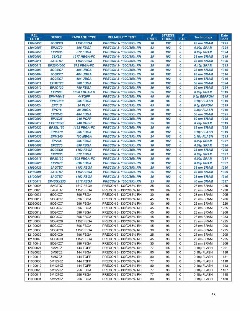
38
REL LOT # DEVICE PACKAGE TYPE RELIABILITY TEST #
UNITS STRESS HOURS
# FAIL Technology Date
Code 13040053 5CGXC9 1152 FBGA PRECON 3- 130C/85% RH 30 192 0 28 nm SRAM 1225 13040057 EP2C70 896 FBGA PRECON 3- 130C/85% RH 53 192 0 0.09µ SRAM 1324 13040058 EP2C35 672 FBGA PRECON 3- 130C/85% RH 30 192 0 0.09µ SRAM 1324 13050006 5SX9E 1517 HBGA-FC PRECON 4- 130C/85% RH 25 192 0 28 nm SRAM 1319 13050011 5AGTD7 1152 FBGA PRECON 3- 130C/85% RH 25 192 0 28 nm SRAM 1320 13050018 EP20K400C 672 FBGA-FC PRECON 3- 130C/85% RH 25 96 0 0.15µ SRAM 1313 13060003 5CGXC7 484 UBGA PRECON 3- 130C/85% RH 30 192 0 28 nm SRAM 1316 13060004 5CGXC7 484 UBGA PRECON 3- 130C/85% RH 30 192 0 28 nm SRAM 1316 13060005 5CGXC7 484 UBGA PRECON 3- 130C/85% RH 30 192 0 28 nm SRAM 1316 13060011 EP3C120 780 FBGA PRECON 3- 130C/85% RH 30 192 0 60 nm SRAM 1324 13060012 EP3C120 780 FBGA PRECON 3- 130C/85% RH 30 192 0 60 nm SRAM 1324 13060020 EP2S90 1020 FBGA-FC PRECON 3- 130C/85% RH 25 192 0 0.09µ SRAM 1319 13060021 EPM7064S 44TQFP PRECON 3- 130C/85% RH 45 96 0 0.5µ EEPROM 1319 13060022 EPM2210 256 FBGA PRECON 3- 130C/85% RH 30 96 0 0.18µ FLASH 1319 13060024 EPC1S 20 PLCC PRECON 3- 130C/85% RH 45 96 0 0.5µ EPROM 1319 13070005 EPC16 88 UBGA PRECON 3- 130C/85% RH 30 96 0 0.35µ FLASH 1319 13070006 EP3C40 484 FBGA PRECON 3- 130C/85% RH 28 192 0 60 nm SRAM 1325 13070009 EP3C25 240 PQFP PRECON 3- 130C/85% RH 30 192 0 60 nm SRAM 1325 13070017 EPF10K70 240 RQFP PRECON 3- 130C/85% RH 25 96 0 0.42µ SRAM 1319 13070022 EP3SL150 1152 FBGA-FC PRECON 3- 130C/85% RH 25 96 0 65 nm SRAM 1325 13070024 EPM570 256 FBGA PRECON 3- 130C/85% RH 30 192 0 0.18µ FLASH 1319 13070032 EPM240 100 MBGA PRECON 3- 130C/85% RH 24 192 0 0.18µ FLASH 1313 13080023 EP2C5 256 FBGA PRECON 3- 130C/85% RH 30 192 0 0.09µ SRAM 1331 13090002 EP2C70 896 FBGA PRECON 3- 130C/85% RH 30 192 0 0.09µ SRAM 1336 13090004 5CGXC9 1152 FBGA PRECON 3- 130C/85% RH 30 192 0 28 nm SRAM 1225 13090007 EP2C35 672 FBGA PRECON 3- 130C/85% RH 30 192 0 0.09µ SRAM 1331 13090015 EP2S130 1508 FBGA-FC PRECON 3- 130C/85% RH 25 96 0 0.09µ SRAM 1331 13090020 EP2C70 896 FBGA PRECON 3- 130C/85% RH 28 192 0 0.09µ SRAM 1331 13090029 5AGTD7 1152 FBGA PRECON 3- 130C/85% RH 25 192 0 28 nm SRAM 1320 13100001 5AGTD7 1152 FBGA PRECON 3- 130C/85% RH 25 192 0 28 nm SRAM 1339 13100007 5AGTD7 1152 FBGA PRECON 3- 130C/85% RH 25 192 0 28 nm SRAM 1340 13100011 EP4SGX230 1517 FBGA PRECON 3- 130C/85% RH 25 96 0 40 nm SRAM 1337 12100008 5AGTD7 1517 FBGA PRECON 3- 130oC/85% RH 25 192 0 28 nm SRAM 1235 12100025 5AGTD7 1152 FBGA PRECON 3- 130oC/85% RH 30 192 0 28 nm SRAM 1236 12040031 5CGXC7 896 FBGA PRECON 3- 130oC/85% RH 30 96 0 28 nm SRAM 1205 12060017 5CGXC7 896 FBGA PRECON 3- 130oC/85% RH 45 96 0 28 nm SRAM 1206 12060033 5CGXC7 896 FBGA PRECON 3- 130oC/85% RH 30 96 0 28 nm SRAM 1226 12060035 5CGXC7 896 FBGA PRECON 3- 130oC/85% RH 45 96 0 28 nm SRAM 1225 12080012 5CGXC7 896 FBGA PRECON 3- 130oC/85% RH 45 96 0 28 nm SRAM 1206 12080030 5CGXC7 896 FBGA PRECON 3- 130oC/85% RH 45 96 0 28 nm SRAM 1233 12100003 5CGXC9 1152 FBGA PRECON 3- 130oC/85% RH 30 96 0 28 nm SRAM 1225 12100027 5CGXC7 896 FBGA PRECON 3- 130oC/85% RH 45 96 0 28 nm SRAM 1206 12100030 5CGXC9 1152 FBGA PRECON 3- 130oC/85% RH 30 96 0 28 nm SRAM 1225 12100032 5CGXC9 896 FBGA PRECON 3- 130oC/85% RH 25 96 0 28 nm SRAM 1205 12110040 5CGXC9 1152 FBGA PRECON 3- 130oC/85% RH 45 96 0 28 nm SRAM 1225 12110042 5CGXC7 896 FBGA PRECON 3- 130oC/85% RH 30 96 0 28 nm SRAM 1206 12020024 5M240Z 144 TQFP PRECON 3- 130oC/85% RH 77 192 0 0.18µ FLASH 1201 11090026 5M570Z 144 FBGA PRECON 3- 130oC/85% RH 80 96 0 0.18µ FLASH 1136 11120013 5M570Z 144 TQFP PRECON 3- 130oC/85% RH 80 96 0 0.18µ FLASH 1131 11050006 5M1270Z 144 TQFP PRECON 3- 130oC/85% RH 77 96 0 0.18µ FLASH 1118 11120012 5M1270Z 144 TQFP PRECON 3- 130oC/85% RH 80 96 0 0.18µ FLASH 1143 11030028 5M1270Z 256 FBGA PRECON 3- 130oC/85% RH 77 96 0 0.18µ FLASH 1107 11050011 5M1270Z 256 FBGA PRECON 3- 130oC/85% RH 77 96 0 0.18µ FLASH 1118 11080001 5M2210Z 256 FBGA PRECON 3- 130oC/85% RH 80 96 0 0.18µ FLASH 1130
39
REL LOT # DEVICE PACKAGE TYPE RELIABILITY TEST #
UNITS STRESS HOURS
# FAIL Technology Date
Code 11080022 5M2210Z 256 FBGA PRECON 3- 130oC/85% RH 80 192 0 0.18µ FLASH 1134 12010017 5M2210Z 256 FBGA PRECON 3- 130oC/85% RH 77 192 0 0.18µ FLASH 1201 11060002 5SGXA7 1517 FBGA PRECON 4- 130oC/85% RH 20 96 0 28 nm SRAM 1122 12020026 5SGXA7 1760 FBGA PRECON 4- 130oC/85% RH 30 192 0 28 nm SRAM 1202 11090002 5SGXA7 1932 FBGA PRECON 4- 130oC/85% RH 25 192 0 28 nm SRAM 1135 12050032 5SGXB6 1517 FBGA PRECON 4- 130oC/85% RH 30 192 0 28 nm SRAM 1205 12090027 5SGXAB 1932 FBGA PRECON 4- 130oC/85% RH 30 192 0 28 nm SRAM 1209 12110034 5SGXAB 1932 FBGA PRECON 4- 130oC/85% RH 30 192 0 28 nm SRAM 1211 13010053 5SGXAB 1517 FBGA PRECON 4- 130oC/85% RH 30 192 0 28 nm SRAM 1301 11060013 EP1C3 144 TQFP PRECON 3- 130oC/85% RH 77 96 0 0.13µ SRAM 1137 12110047 EP1C6 144 TQFP PRECON 3- 121°C/100% RH 77 96 0 0.13µ SRAM 1219 12010023 EP1S40 1508 FBGA PRECON 3- 130oC/85% RH 25 96 0 0.13µ SRAM 1149 12080035 EP1S80 1508 FBGA PRECON 3- 130oC/85% RH 25 96 0 0.13µ SRAM 1219 11100016 EP20K100 208 PQFP PRECON 3- 130oC/85% RH 25 96 0 0.22µ SRAM 1119 12050013 EP20K100B 356BGA PRECON 3- 130oC/85% RH 25 96 0 0.22µ SRAM 1213 12020014 EP20K100E 240 PQFP PRECON 3- 130oC/85% RH 25 96 0 0.18µ SRAM 1125 11080018 EP20K160E 356 BGA PRECON 3- 130oC/85% RH 25 96 0 0.18µ SRAM 1101 12110011 EP20K160E 356 BGA PRECON 3- 130oC/85% RH 25 96 0 0.18µ SRAM 1237 11040003 EP20K300E 672 FBGA PRECON 3- 130oC/85% RH 28 96 0 0.18µ SRAM 1115 11050015 EP20K400C 672 FBGA PRECON 3- 130oC/85% RH 25 96 0 0.15µ SRAM 1121 12070008 EP20K400C 672 FBGA PRECON 3- 130oC/85% RH 25 96 0 0.15µ SRAM 1121 12120017 EP2AGX125 1152 FBGA PRECON 3- 130oC/85% RH 25 192 0 40 nm SRAM 1237 11120001 EP2AGX190 780 FBGA PRECON 3- 130oC/85% RH 24 192 0 40 nm SRAM 1131 12050039 EP2AGX260 1152 FBGA PRECON 3- 130oC/85% RH 25 192 0 40 nm SRAM 1205 11060014 EP2C8 256 FBGA PRECON 3- 130oC/85% RH 25 96 0 0.09µ SRAM 1126 12040001 EP2C8 144 TQFP PRECON 3- 130oC/85% RH 80 192 0 0.09µ SRAM 1207 12080006 EP2C8 144 TQFP PRECON 3- 130oC/85% RH 77 192 0 0.09µ SRAM 1225 12100012 EP2C8 208 PQFP PRECON 3- 130oC/85% RH 77 192 0 0.09µ SRAM 1231 11030026 EP2C20 256 FBGA PRECON 3- 130oC/85% RH 77 96 0 0.09µ SRAM 1049 12080037 EP2C20 240PQFP PRECON 3- 130oC/85% RH 77 192 0 0.09µ SRAM 1231 12110006 EP2C20 256 FBGA PRECON 3- 130oC/85% RH 77 96 0 0.09µ SRAM 1243 12030025 EP2C70 672FBGA PRECON 3- 130oC/85% RH 77 192 0 0.09µ SRAM 1207 12040022 EP2C70 672FBGA PRECON 3- 130oC/85% RH 77 192 0 0.09µ SRAM 1207 12050035 EP2C70 672FBGA PRECON 3- 130oC/85% RH 77 192 0 0.09µ SRAM 1207 11100005 EP2C70 672 FBGA PRECON 3- 130oC/85% RH 77 96 0 0.09µ SRAM 1119 12070001 EP2C70 672 FBGA PRECON 3- 130oC/85% RH 77 96 0 0.09µ SRAM 1207 12090011 EP2C70 672 FBGA PRECON 3- 130oC/85% RH 77 96 0 0.09µ SRAM 1219 12120018 EP2C90 240 PQFP PRECON 3- 130oC/85% RH 77 192 0 0.09µ SRAM 1243 12040010 EP2S90 1508 FBGA PRECON 3- 130oC/85% RH 25 96 0 0.09µ SRAM 1207 11060011 EP2S90 1020 FBGA PRECON 3- 130oC/85% RH 25 96 0 0.09µ SRAM 1125 12090020 EP2S90 1508 FBGA PRECON 3- 130oC/85% RH 25 96 0 0.09µ SRAM 1213 11120011 EP2S130 1508 FBGA PRECON 3- 130oC/85% RH 25 96 0 0.09µ SRAM 1119 11040006 EP3C16 144 EQFP PRECON 3- 130oC/85% RH 78 96 0 60 nm SRAM 1116 12110012 EP3C25 144 EQFP PRECON 3- 130oC/85% RH 77 192 0 60 nm SRAM 1237 11080002 EP3C40 240 PQFP PRECON 3- 130oC/85% RH 77 96 0 60 nm SRAM 1119 11040001 EP3C80 484 UBGA PRECON 3- 130oC/85% RH 80 96 0 60 nm SRAM 1127 11050010 EP3C80 484 UBGA PRECON 3- 130oC/85% RH 78 96 0 60 nm SRAM 1101 11040010 EP3C120 780 FBGA PRECON 3- 130oC/85% RH 77 96 0 60 nm SRAM 1117 11040013 EP3C120 780 FBGA PRECON 3- 130oC/85% RH 77 96 0 60 nm SRAM 1117 12040030 EP3C120 780 FBGA PRECON 3- 130oC/85% RH 77 192 0 60 nm SRAM 1213 12060015 EP3C120 780 FBGA PRECON 3- 130oC/85% RH 77 96 0 60 nm SRAM 1222 11060010 EP3C120 780 FBGA PRECON 3- 130oC/85% RH 30 96 0 60 nm SRAM 1124 12040012 EP3C120 780 FBGA PRECON 3- 130oC/85% RH 24 96 0 60 nm SRAM 1214 11030015 EP3SE50 780 FBGA PRECON 3- 130oC/85% RH 25 96 0 65 nm SRAM 1043
40
REL LOT # DEVICE PACKAGE TYPE RELIABILITY TEST #
UNITS STRESS HOURS
# FAIL Technology Date
Code 12100005 EP3SE50 780 FBGA PRECON 3- 130oC/85% RH 25 96 0 65 nm SRAM 1237 11070014 EP3SL50 780 FBGA PRECON 3- 130oC/85% RH 25 96 0 65 nm SRAM 1112 11100002 EP3SL150 1152 FBGA PRECON 3- 130oC/85% RH 25 96 0 65 nm SRAM 1119 12070022 EP3SL150 1152 FBGA PRECON 3- 130oC/85% RH 25 96 0 65 nm SRAM 1225 11080004 EP3SL200 1152 FBGA PRECON 3- 130oC/85% RH 25 96 0 65 nm SRAM 1049 12010021 EP3SL200 1152 FBGA PRECON 3- 130oC/85% RH 25 96 0 65 nm SRAM 1146 11050008 EP4CGX15 148 QFN PRECON 3- 130oC/85% RH 80 96 0 60 nm SRAM 1119 11100015 EP4CGX15 148 QFN PRECON 3- 130oC/85% RH 77 96 0 60 nm SRAM 1131 12080036 EP4CGX15 148 QFN PRECON 3- 130oC/85% RH 77 192 0 60 nm SRAM 1131 11070025 EP4CGX150 896 PBGA PRECON 3- 130oC/85% RH 77 96 0 60 nm SRAM 1119 12020033 EP4CGX150 896 FBGA PRECON 3- 130oC/85% RH 77 192 0 60 nm SRAM 1201 11030012 EP4SGX230 1517 FBGA PRECON 3- 130oC/85% RH 25 96 0 40 nm SRAM 1108 12080033 EP4SGX230 1517 FBGA PRECON 3- 130oC/85% RH 25 192 0 40 nm SRAM 1208 11120033 EP4SGX230 1517 FBGA PRECON 3- 130oC/85% RH 22 192 0 40 nm SRAM 1137 11010001 EP4SGX530 1517 HBGA PRECON 4- 130oC/85% RH 25 192 0 40 nm SRAM 1101 12050041 EP4SGX530 1517HBGA PRECON 3- 130oC/85% RH 25 96 0 40 nm SRAM 1205 11090028 EPC1 20 PLCC PRECON 3- 130oC/85% RH 45 96 0 0.5µ EPROM 1127 12080001 EPC1 20 PLCC PRECON 3- 130oC/85% RH 45 96 0 0.5µ EPROM 1230 12080001 EPC1S 20 PLCC PRECON 3- 121°C/100% RH 45 96 0 0.5µ EPROM 1230 12030019 EPC1441 20 PLCC PRECON 3- 130oC/85% RH 45 96 0 0.5µ EPROM 1207 11120037 EPC16 100 PQFP PRECON 3- 130oC/85% RH 45 96 0 0.35µ FLASH 1142 12100009 EPC16 88 UBGA PRECON 3- 130oC/85% RH 45 96 0 0.35µ FLASH 1231 11080010 EPC2 20 PLCC PRECON 3- 130oC/85% RH 45 96 0 0.4µ FLASH 1113 12020028 EPC2 20 PLCC PRECON 3- 130oC/85% RH 45 96 0 0.4µ FLASH 1204 11040014 EPF10K70 240 RQFP PRECON 3- 130oC/85% RH 25 96 0 0.42µ SRAM 1107 12090012 EPF10K70 240 RQFP PRECON 3- 130oC/85% RH 25 96 0 0.42µ SRAM 1231 12030028 EPF10K100E 208 PQFP PRECON 3- 130oC/85% RH 25 96 0 0.22µ SRAM 1143 11030014 EPF6016 208 PQFP PRECON 3- 130oC/85% RH 25 96 0 0.42µ SRAM 1101 12090021 EPF6016 208 PQFP PRECON 3- 130oC/85% RH 25 96 0 0.42µ SRAM 1225 12030039 EPM1270 256 FBGA PRECON 3- 121°C/100% RH 69 96 0 0.18µ FLASH 1203 12080031 EPM1270 256 FBGA PRECON 3- 121°C/100% RH 77 96 0 0.18µ FLASH 1219 12040032 EPM1270 144 TQFP PRECON 3- 121°C/100% RH 77 192 0 0.18µ FLASH 1213 12110027 EPM1270 144 TQFP PRECON 3- 121°C/100% RH 77 192 0 0.18µ FLASH 1245 12050002 EPM2210G 324 FBGA PRECON 3- 130oC/85% RH 77 96 0 0.18µ FLASH 1206 12060014 EPM2210G 256 FBGA PRECON 3- 130oC/85% RH 80 96 0 0.18µ FLASH 1207 12030003 EPM240 100 TQFP PRECON 3- 130oC/85% RH 65 192 0 0.18µ FLASH 1207 12120006 EPM240 100 MBGA PRECON 3- 130oC/85% RH 77 192 0 0.18µ FLASH 1243 11030013 EPM240Z 100 MBGA PRECON 3- 130oC/85% RH 77 96 0 0.18µ FLASH 1101 11070012 EPM570 100 TQFP PRECON 3- 130oC/85% RH 78 96 0 0.18µ FLASH 1128 11100003 EPM3064A 44 TQFP PRECON 3- 130oC/85% RH 45 96 0 0.35µ EEPROM 1125 11040002 EPM7064 44 PLCC PRECON 3- 130oC/85% RH 45 96 0 0.5µ EEPROM 1101 12080009 EPM7064AE 100 TQFP PRECON 3- 121oC/100% RH 45 96 0 0.3µ EEPROM 1230 12110039 EPM7064S 44 TQFP PRECON 3- 121°C/100% RH 45 96 0 0.5µ EEPROM 1237 12040011 EPM7512AE 208 PQFP PRECON 3- 130oC/85% RH 25 96 0 0.35µ EEPROM 1207 11070008 EPM7512AE 208 PQFP PRECON 3- 130oC/85% RH 25 96 0 0.35µ EEPROM 1119

41
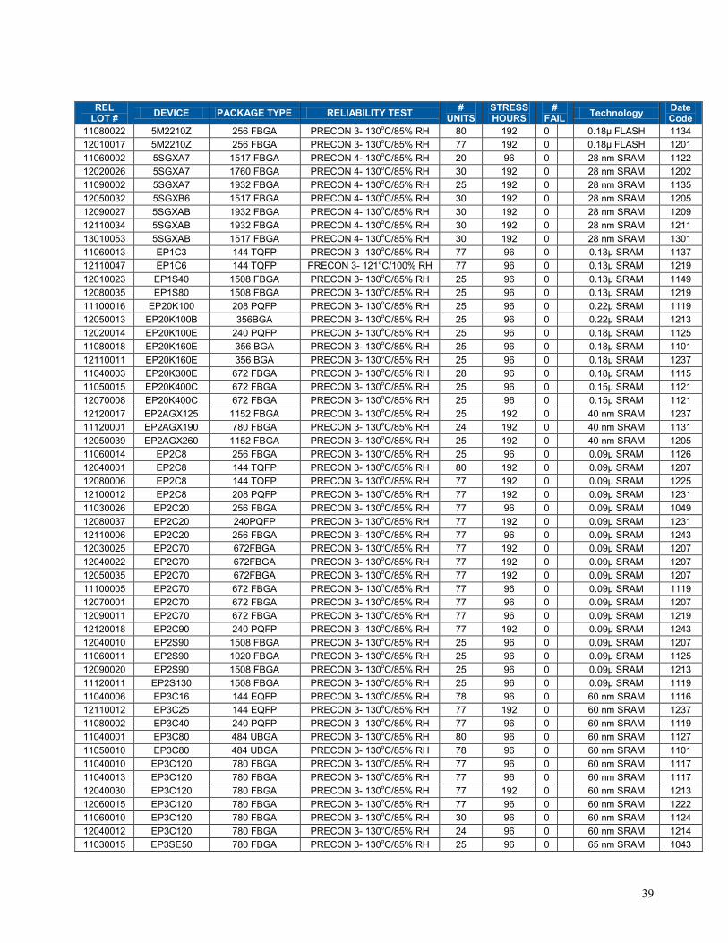
Temperature Humidity Bias Reference: JESD22-A101 (JEDEC Standard) All lots are subjected to Biased Humidity test after being preconditioned to JEDEC standard moisture sensitivity level (MSL) and subjected to a 3X reflow. Stress can last up to 2000 Hrs.
Temperature Humidity Bias Results
REL LOT # DEVICE PACKAGE TYPE RELIABILITY TEST #
UNITS STRESS HOURS
# FAIL Technology Date
Code 13010017 EP4CGX150 896 FBGA PRECON 3-85/85THB 30 1000 0 60nm SRAM 1243 13010060 EP3SL200 1152 FBGA-FC PRECON 3-85/85THB 25 1000 0 65nm SRAM 1237 13010060 EP2C70 672 FBGA PRECON 3-85/85THB 30 1000 0 0.09µ SRAM 1243 13010063 EP2C70 672 FBGA PRECON 3-85/85THB 60 1000 0 0.09µ SRAM 1249 13030016 EP1S40Z 1020 FBGA-FC PRECON 3-85/85THB 25 1000 0 0.13µ SRAM 1307 13030022 EP3C16 256 FBGA PRECON 3-85/85THB 30 1000 0 60 nm SRAM 1301 13040006 EP2AGX260 1152 FBGA-FC PRECON 3-85/85THB 25 1000 0 40 nm SRAM 1307 13040011 EP3C120 780 FBGA PRECON 3-85/85THB 30 1000 0 60 nm SRAM 1307 13040031 EP2C35 672 FBGA PRECON 3-85/85THB 30 1000 0 0.09µ SRAM 1313 13040042 EP2S90 1020 FBGA-FC PRECON 3-85/85THB 25 1000 0 0.09µ SRAM 1307 13050011 5AGTD7 1152 FBGA PRECON 3-85/85THB 25 1000 0 28 nm SRAM 1320 13050018 EP20K400C 672 FBGA-FC PRECON 3-85/85THB 25 1000 0 0.15µ SRAM 1313 13060020 EP2S90 1020 FBGA-FC PRECON 3-85/85THB 25 1000 0 0.09µ SRAM 1319 13070009 EP3C25 240 PQFP PRECON 3-85/85THB 30 2000 0 60 nm SRAM 1325 13070010 EP4CGX150 896 FPGA PRECON 3-85/85THB 30 1000 0 60 nm SRAM 1325 13070016 5SX9E 1932 FBGA-FC PRECON 4-85/85THB 30 1000 0 28 nm SRAM 1325 13070022 EP3SL150 1152 FBGA-FC PRECON 3-85/85THB 25 1000 0 65 nm SRAM 1325 12100008 5AGTD7 1517 FBGA PRECON 3-85/85THB 24 1000 0 28 nm SRAM 1235 12040021 5CGXC7 896 FBGA PRECON 3-85/85THB 30 1000 0 28 nm SRAM 1205 12040031 5CGXC7 896 FBGA PRECON 3-85/85THB 30 1000 0 28 nm SRAM 1205 12060017 5CGXC7 896 FBGA PRECON 3-85/85THB 27 1000 0 28 nm SRAM 1206 12060035 5CGXC7 896 FBGA PRECON 3-85/85THB 27 1000 0 28 nm SRAM 1225 12080012 5CGXC7 896 FBGA PRECON 3-85/85THB 27 1000 0 28 nm SRAM 1206 12080030 5CGXC7 896 FBGA PRECON 3-85/85THB 27 1000 0 28 nm SRAM 1233 12100003 5CGXC9 1152 FBGA PRECON 3-85/85THB 30 1000 0 28 nm SRAM 1225 12100027 5CGXC7 896 FBGA PRECON 3-85/85THB 27 1000 0 28 nm SRAM 1206 12100030 5CGXC9 1152 FBGA PRECON 3-85/85THB 30 1000 0 28 nm SRAM 1225 12100032 5CGXC9 896 FBGA PRECON 3-85/85THB 25 1000 0 28 nm SRAM 1205 12110040 5CGXC9 1152 FBGA PRECON 3-85/85THB 30 1000 0 28 nm SRAM 1225 12110042 5CGXC7 896 FBGA PRECON 3-85/85THB 30 1000 0 28 nm SRAM 1206 11060002 5SGXA7 1517 FBGA PRECON 4-85/85THB 25 1000 0 28 nm SRAM 1122 11090002 5SGXA7 1932 FBGA PRECON 4-85/85THB 23 1000 0 28 nm SRAM 1136 11110038 5SGXA7 1517 FBGA PRECON 4-85/85THB 30 1000 0 28 nm SRAM 1110 12030040 5SGXA7 1517 FBGA PRECON 4-85/85THB 30 1000 0 28 nm SRAM 1203 12050021 5SGXA7 1517 FBGA PRECON 4-85/85THB 30 1000 0 28 nm SRAM 1205 12090027 5SGX9E 1932 FBGA PRECON 4-85/85THB 30 1000 0 28 nm SRAM 1209 12110034 5SGX9E 1932 FBGA PRECON 4-85/85THB 30 1000 0 28 nm SRAM 1211 11030011 EP1S40 1508 FBGA PRECON 3-85/85THB 25 1000 0 0.13µ SRAM 1001 12010023 EP1S40 1508 FBGA PRECON 3-85/85THB 25 1000 0 0.13µ SRAM 1149 12080035 EP1S80 1508 FBGA PRECON 3-85/85THB 25 1000 0 0.13µ SRAM 1219 12050013 EP20K100N 356 BGA PRECON 3-85/85THB 25 1000 0 0.22µ SRAM 1213 11080018 EP20K160E 356 BGA PRECON 3-85/85THB 25 1000 0 0.18µ SRAM 1101 12110011 EP20K160E 356 BGA PRECON 3-85/85THB 25 1000 0 0.18µ SRAM 1237 10090008 EP20K400C 672 FBGA PRECON 3-85/85THB 25 1000 0 0.15µ SRAM 1031 11050015 EP20K400C 672 FBGA PRECON 3-85/85THB 25 1000 0 0.15µ SRAM 1121

42
REL LOT # DEVICE PACKAGE TYPE RELIABILITY TEST #
UNITS STRESS HOURS
# FAIL Technology Date
Code 12070008 EP20K400C 672 FBGA PRECON 3-85/85THB 25 1000 0 0.15µ SRAM 1201 12120017 EP2AGX125 1152 FBGA PRECON 3-85/85THB 27 2000 0 40 nm SRAM 1237 12050039 EP2AGX260 1152 FBGA PRECON 3-85/85THB 25 1000 0 40 nm SRAM 1205 11080019 EP2C20 256 FBGA PRECON 3-85/85THB 77 1000 0 0.09µ SRAM 1107 11100005 EP2C70 672 FBGA PRECON 3-85/85THB 25 1000 0 0.09µ SRAM 1119 12030025 EP2C70 672 FBGA PRECON 3-85/85THB 77 1000 0 0.09µ SRAM 1207 12050035 EP2C70 672 FBGA PRECON 3-85/85THB 77 2000 0 0.09µ SRAM 1207 12070001 EP2C70 672 FBGA PRECON 3-85/85THB 77 2000 0 0.09µ SRAM 1207 12090011 EP2C70 672 FBGA PRECON 3-85/85THB 77 1000 0 0.09µ SRAM 1219 11060011 EP2S90 1020 FBGA PRECON 3-85/85THB 25 1000 0 0.09µ SRAM 1125 12040018 EP2S90 1020 FBGA PRECON 3-85/85THB 25 1000 0 0.09µ SRAM 1207 11030025 EP2S130 1508 FBGA PRECON 3-85/85THB 25 1000 0 0.09µ SRAM 1011 11090017 EP3C10 256 FBGA PRECON 3-85/85THB 22 1000 0 60 nm SRAM 1130 11040006 EP3C16 144 EQFP PRECON 3-85/85THB 78 1000 0 60 nm SRAM 1116 11060006 EP3C40 240 PQFP PRECON 3-85/85THB 77 1000 0 60 nm SRAM 1113 11050010 EP3C80 484 UBGA PRECON 3-85/85THB 90 1000 0 60 nm SRAM 1101 11040001 EP3C80 484 UBGA PRECON 3-85/85THB 28 1000 0 60 nm SRAM 1127 11040010 EP3C120 780 FBGA PRECON 3-85/85THB 26 1000 0 60 nm SRAM 1117 11040013 EP3C120 780 FBGA PRECON 3-85/85THB 29 1000 0 60 nm SRAM 1117 12040030 EP3C120 780 FBGA PRECON 3-85/85THB 77 2000 0 60 nm SRAM 1213 12060015 EP3C120 780 FBGA PRECON 3-85/85THB 77 1000 0 60 nm SRAM 1222 11030015 EP3SE50 780 FBGA PRECON 3-85/85THB 25 1000 0 65 nm SRAM 1043 12070022 EP3SL150 1152 FBGA PRECON 3-85/85THB 25 1000 0 65 nm SRAM 1225 11080004 EP3SL200 1152 FBGA PRECON 3-85/85THB 25 1000 0 65 nm SRAM 1049 11070014 EP3SL50 780 FBGA PRECON 3-85/85THB 25 1012 0 65 nm SRAM 1112 11030010 EP4CGX15 148 QFN PRECON 3-85/85THB 77 1000 0 60 nm SRAM 1101 11050008 EP4CGX15 148 QFN PRECON 3-85/85THB 80 1000 0 60 nm SRAM 1119 11100015 EP4CGX15 148 QFN PRECON 3-85/85THB 77 2000 0 60 nm SRAM 1131 12080036 EP4CGX15 148 QFN PRECON 3-85/85THB 77 2000 0 60 nm SRAM 1231 11070025 EP4CGX150 896 FBGA PRECON 3-85/85THB 76 1000 0 60 nm SRAM 1119 11030012 EP4SGX230 1517 FBGA PRECON 3-85/85THB 24 1000 0 40 nm SRAM 1108 12050042 EP4SGX230 1517 FBGA PRECON 3-85/85THB 25 1000 0 40 nm SRAM 1205 12080033 EP4SGX230 1517 FBGA PRECON 3-85/85THB 25 1000 0 40 nm SRAM 1208 11040002 EPM7064 44 PLCC PRECON 3-85/85THB 45 1000 0 0.5µ EPROM 1101

43
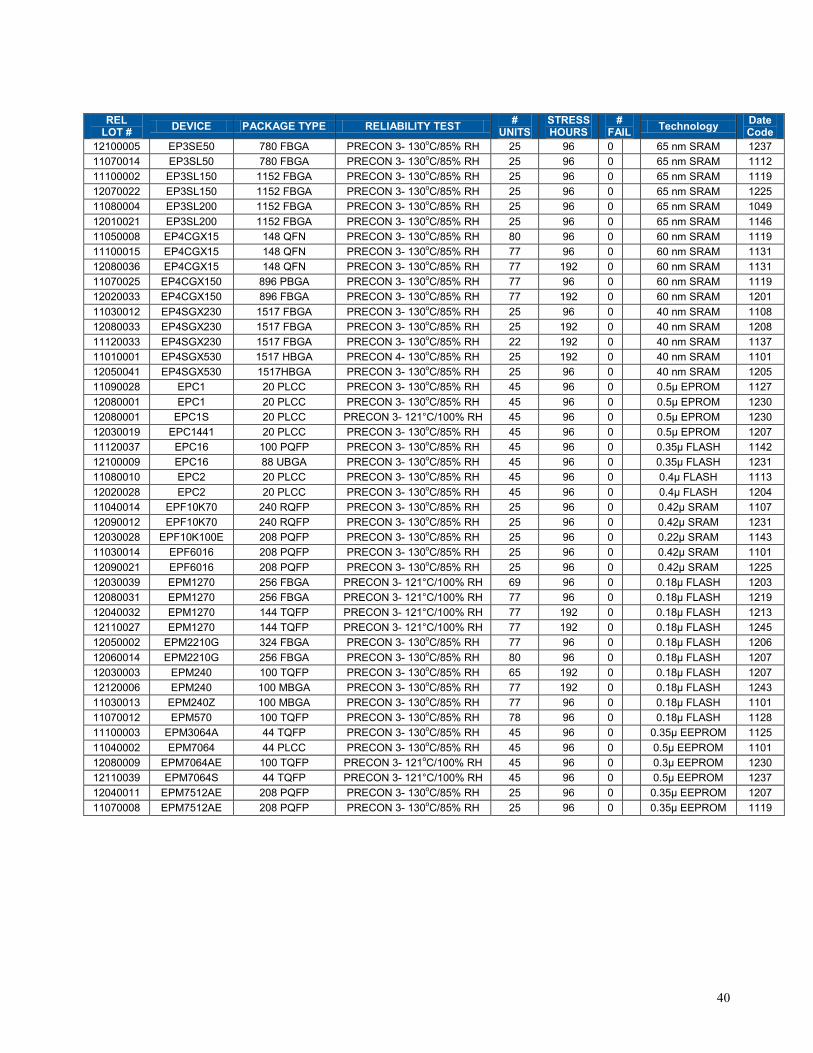
Highly Accelerated Stress Testing Reference: JESD22-A110 (JEDEC Standard) All lots are subjected to HAST test after being preconditioned to JEDEC standard moisture sensitivity level (MSL) and subjected to a 3X reflow HAST Results
REL LOT # DEVICE PACKAGE
TYPE RELIABILITY TEST # UNITS STRESS HOURS
# FAIL Technology Date
Code 13010011 EP2C8 256 FBGA PRECON 3-HAST 30 192 0 0.09µ SRAM 1243 12010054 EPC1S 20 PLCC PRECON 3-HAST 45 96 0 0.5µ EPROM 1249 13020067 EPM1270 256 FBGA PRECON 3-HAST 30 96 0 0.18µ FLASH 1243 13020080 EPC2 20 PLCC PRECON 3-HAST 45 96 0 0.4µ FLASH 1301 13030014 EPF10K50A 356 SBGA PRECON 3-HAST 25 96 0 0.3µ SRAM 1243 13030019 EPM22100 100 PQFP PRECON 3-HAST 30 192 0 0.18µ FLASH 1313 13030062 EPF10K100E 208 PQFP PRECON 3-HAST 25 96 0 0.22µ SRAM 1307 13040019 EPM2210 100 PQFP PRECON 3-HAST 30 96 0 0.18µ FLASH 1315 13040020 EPM2210 100 PQFP PRECON 3-HAST 30 96 0 0.18µ FLASH 1315 13040025 EPM2210 100 PQFP PRECON 3-HAST 30 96 0 0.18µ FLASH 1315 13040026 EPM240 100 TQFP PRECON 3-HAST 25 192 0 0.18µ FLASH 1307 13040027 EPM2210 100 PQFP PRECON 3-HAST 30 96 0 0.18µ FLASH 1315 13040028 EPM2210 100 PQFP PRECON 3-HAST 30 96 0 0.18µ FLASH 1315 13040029 EPM2210 100 PQFP PRECON 3-HAST 30 96 0 0.18µ FLASH 1315 13040032 EP2C5 208 PQFP PRECON 3-HAST 30 192 0 0.09µ SRAM 1313 13040033 EP2C8 256 FBGA PRECON 3-HAST 30 192 0 0.09µ SRAM 1315 13040044 EPM1270 144 TQFP PRECON 3-HAST 29 96 0 0.18µ FLASH 1307 13050012 EP2C8 208 PQFP PRECON 3-HAST 30 192 0 0.09µ SRAM 1313 13050015 EP2C8 256 FBGA PRECON 3-HAST 30 96 0 0.09µ SRAM 1313 13060021 EPM7064S 44 TQFP PRECON 3-HAST 45 96 0 0.5µ EEPROM 1319 13060022 EPM2210 256 FBGA PRECON 3-HAST 30 96 0 0.18µ FLASH 1319 13060024 EPC1S 20 PLCC PRECON 3-HAST 45 96 0 0.5µ EPROM 1319 13060035 EP1C4 400 FBGA PRECON 3-HAST 30 96 0 0.13µ SRAM 1324 13070005 EPC16 88 UBGA PRECON 3-HAST 30 96 0 0.35u FLASH 1319 13070012 EP2C8 256 FBGA PRECON 3-HAST 30 192 0 0.09µ SRAM 1325 13070017 EPF10K70 240 RQFP PRECON 3-HAST 25 96 0 0.42µ SRAM 1319 13070024 EPM570 256 FBGA PRECON 3-HAST 30 192 0 0.18µ FLASH 1319 13080004 EPM1270 256 FBGA PRECON 3-HAST 35 192 0 0.18µ FLASH 1319 13080005 EPM570 256 FBGA PRECON 3-HAST 35 192 0 0.18µ FLASH 1325 13080006 EP2C8 256 FBGA PRECON 3-HAST 30 192 0 0.09µ SRAM 1325 13080023 EP2C5 256 FBGA PRECON 3-HAST 30 192 0 0.09µ SRAM 1331 12020024 5M240Z 144 TQFP PRECON 3-HAST. 77 192 0 0.18µ FLASH 1201 11120013 5M570Z 144 TQFP PRECON 3-HAST 80 96 0 0.18µ FLASH 1131 11090026 5M570Z 144 FBGA PRECON 3-HAST 80 96 0 0.18µ FLASH 1136 11050006 5M1270Z 144 TQFP PRECON 3-HAST 75 96 0 0.18µ FLASH 1118 11060012 5M1270Z 144 TQFP PRECON 3-HAST 77 96 0 0.18µ FLASH 1123 11030028 5M1270Z 256 FBGA PRECON 3-HAST 77 96 0 0.18µ FLASH 1107 11050011 5M1270Z 256 FBGA PRECON 3-HAST 77 96 0 0.18µ FLASH 1118 11080021 5M2210Z 256 FBGA PRECON 3-HAST 79 192 0 0.18µ FLASH 1134 11080022 5M2210Z 256 FBGA PRECON 3-HAST 78 192 0 0.18µ FLASH 1134 12010017 5M2210Z 256 FBGA PRECON 3-HAST 77 192 0 0.18µ FLASH 1201 11060013 EP1C3 144 TQFP PRECON 3-HAST 77 96 0 0.13µ SRAM 1137 12040014 EP1C4 400 FBGA PRECON 3-HAST 77 96 0 0.13µ SRAM 1204

44
REL LOT # DEVICE PACKAGE
TYPE RELIABILITY TEST # UNITS STRESS HOURS
# FAIL Technology Date
Code 12110047 EP1C8 144 TQFP PRECON 3-HAST 77 96 0 0.13µ SRAM 1219 11110022 EP1C20 324 FBGA PRECON 3-HAST 77 96 0 0.13µ SRAM 1119 12080001 EP1S 20PLCC PRECON 3-HAST 45 96 0 0.5µ EEPROM 1230 11100016 EP20K100 208 PQFP PRECON 3-HAST 25 96 0 0.22µ SRAM 1119 12020014 EP20K100E 240 PQFP PRECON 3-HAST 25 96 0 0.18µ SRAM 1125 11040003 EP20K300E 672 FBGA PRECON 3-HAST 26 96 0 0.18µ SRAM 1115 12030027 EP2C5Y90 208 PQFP PRECON 3-HAST 30 192 0 0.09µ SRAM 1210 12040033 EP2C5Y91 256 FBGA PRECON 3-HAST 78 192 0 0.09µ SRAM 1207 12050012 EP2C5Y92 256 FBGA PRECON 3-HAST 78 192 0 0.09µ SRAM 1207 12030026 EP2C8 144 TQFP PRECON 3-HAST 56 192 0 0.09µ SRAM 1201 12030050 EP2C8 208 PQFP PRECON 3-HAST 30 192 0 0.09µ SRAM 1213 12040001 EP2C8 144 TQFP PRECON 3-HAST 40 96 0 0.09µ SRAM 1207 12080006 EP2C8 144 TQFP PRECON 3-HAST 77 192 0 0.09µ SRAM 1225 11060014 EP2C8 256 FBGA PRECON 3-HAST 24 192 0 0.09µ SRAM 1126 13010011 EP2C8 256 FBGA PRECON 3-HAST 30 192 0 0.09µ SRAM 1243 12080037 EP2C20 240PQFP PRECON 3-HAST 77 192 0 0.09µ SRAM 1231 12110006 EP2C20 256 FBGA PRECON 3-HAST 77 192 0 0.09µ SRAM 1243 12120018 EP2C20 240 PQFP PRECON 3-HAST 77 96 0 0.09µ SRAM 1243 11090028 EPC1 20 PLCC PRECON 3-HAST 45 96 0 0.5µ EPROM 1127 12030019 EPC1441 20 PLCC PRECON 3-HAST 45 96 0 0.5µ EPROM 1207 11120037 EPC16 100 PQFP PRECON 3-HAST 45 96 0 0.35µ FLASH 1142 12100009 EPC16 88 UBGA PRECON 3-HAST 45 96 0 0.35µ FLASH 1231 11080010 EPC2 20 PLCC PRECON 3-HAST 45 96 0 0.4µ FLASH 1113 12020028 EPC2 20 PLCC PRECON 3-HAST 45 96 0 0.4µ FLASH 1204 12030028 EPF10K100E 208 PQFP PRECON 3-HAST 25 96 0 0.22µ SRAM 1143 11110023 EPF10K100E 356 BGA PRECON 3-HAST 25 96 0 0.22µ SRAM 1131 12030020 EPF10K50 356 BGA PRECON 3-HAST 25 96 0 0.3µ SRAM 1201 11040014 EPF10K70 240 RQFP PRECON 3-HAST 25 96 0 0.42µ SRAM 1107 12090012 EPF10K70 240 RQFP PRECON 3-HAST 25 96 0 0.42µ SRAM 1231 11030014 EPF6016 208 PQFP PRECON 3-HAST 25 96 0 0.42µ SRAM 1101 12090021 EPF6016 208 PQFP PRECON 3-HAST 25 96 0 0.42µ SRAM 1225 12030003 EPM240 100 TQFP PRECON 3-HAST 48 192 0 0.18µ FLASH 1207 11030018 EPM570 100 TQFP PRECON 3-HAST 25 96 0 0.18µ FLASH 1112 11070012 EPM570 100 TQFP PRECON 3-HAST 79 96 0 0.18µ FLASH 1128 1112013 EPM570 144 TQFP PRECON 3-HAST 80 96 0 0.18µ FLASH 1131
12020024 EPM570 144 TQFP PRECON 3-HAST 77 192 0 0.18µ FLASH 1201 12090007 EPM570 144 TQFP PRECON 3-HAST 120 96 0 0.18µ FLASH 1237 12030039 EPM1270 256 FBGA PRECON 3-HAST 56 192 0 0.18µ FLASH 1203 12040032 EPM1270 144 TQFP PRECON 3-HAST 77 192 0 0.18µ FLASH 1213 12080031 EPM1270 256 FBGA PRECON 3-HAST 77 96 0 0.18µ FLASH 1219 12110027 EPM1270 144 TQFP PRECON 3-HAST 77 192 0 0.18µ FLASH 1245 12010017 EPM2210G 256 FBGA PRECON 3-HAST 77 192 0 0.18µ FLASH 1201 12040036 EPM2210 256 FBGA PRECON 3-HAST 76 96 0 0.18µ FLASH 1207 11100003 EPM3064A 44 TQFP PRECON 3-HAST 45 96 0 0.35µ EEPROM 1125 12080009 EPM7064AE 100TQFP PRECON 3-HAST 45 96 0 0.35µ EEPROM 1230 12110039 EPM7064S 44 TQFP PRECON 3-HAST 45 96 0 0.5µ EEPROM 1237 11100018 EPM7256B 256 FBGA PRECON 3-HAST 25 96 0 0.22µ EEPROM 1137 12060013 EPM7256B 256 FBGA PRECON 3-HAST 25 96 0 0.22µ EEPROM 1207 12040011 EPM7512AE 208 PQFP PRECON 3-HAST 25 96 0 0.35µ EEPROM 1207
45
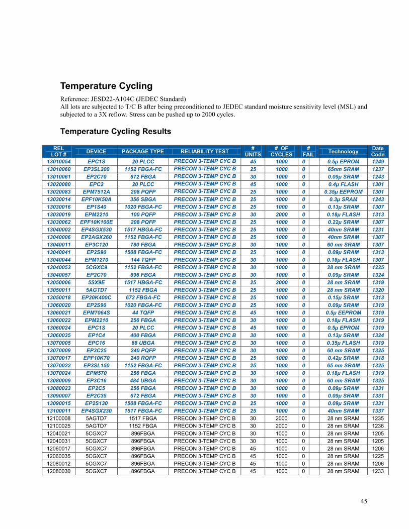
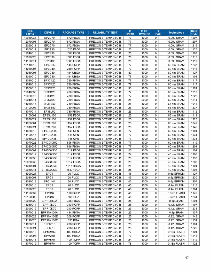
Temperature Cycling Reference: JESD22-A104C (JEDEC Standard) All lots are subjected to T/C B after being preconditioned to JEDEC standard moisture sensitivity level (MSL) and subjected to a 3X reflow. Stress can be pushed up to 2000 cycles. Temperature Cycling Results
REL
LOT # DEVICE PACKAGE TYPE RELIABILITY TEST # UNITS
# OF CYCLES
# FAIL Technology Date
Code 13010054 EPC1S 20 PLCC PRECON 3-TEMP CYC B 45 1000 0 0.5μ EPROM 1249 13010060 EP3SL200 1152 FBGA-FC PRECON 3-TEMP CYC B 25 1000 0 65nm SRAM 1237 13010061 EP2C70 672 FBGA PRECON 3-TEMP CYC B 30 1000 0 0.09μ SRAM 1243 13020080 EPC2 20 PLCC PRECON 3-TEMP CYC B 45 1000 0 0.4μ FLASH 1301 13020083 EPM7512A 208 PQFP PRECON 3-TEMP CYC B 25 1000 0 0.35μ EEPROM 1301 13030014 EPF10K50A 356 SBGA PRECON 3-TEMP CYC B 25 1000 0 0.3μ SRAM 1243 13030016 EP1S40 1020 FBGA-FC PRECON 3-TEMP CYC B 25 1000 0 0.13μ SRAM 1307 13030019 EPM2210 100 PQFP PRECON 3-TEMP CYC B 30 2000 0 0.18μ FLASH 1313 13030062 EPF10K100E 208 PQFP PRECON 3-TEMP CYC B 25 1000 0 0.22μ SRAM 1307 13040002 EP4SGX530 1517 HBGA-FC PRECON 3-TEMP CYC B 25 1000 0 40nm SRAM 1231 13040006 EP2AGX260 1152 FBGA-FC PRECON 3-TEMP CYC B 25 1000 0 40nm SRAM 1307 13040011 EP3C120 780 FBGA PRECON 3-TEMP CYC B 30 1000 0 60 nm SRAM 1307 13040041 EP2S90 1508 FBGA-FC PRECON 3-TEMP CYC B 25 1000 0 0.09μ SRAM 1313 13040044 EPM1270 144 TQFP PRECON 3-TEMP CYC B 30 1000 0 0.18μ FLASH 1307 13040053 5CGXC9 1152 FBGA-FC PRECON 3-TEMP CYC B 30 1000 0 28 nm SRAM 1225 13040057 EP2C70 896 FBGA PRECON 3-TEMP CYC B 30 1000 0 0.09μ SRAM 1324 13050006 5SX9E 1517 HBGA-FC PRECON 4-TEMP CYC B 25 2000 0 28 nm SRAM 1319 13050011 5AGTD7 1152 FBGA PRECON 3-TEMP CYC B 25 1000 0 28 nm SRAM 1320 13050018 EP20K400C 672 FBGA-FC PRECON 3-TEMP CYC B 25 1000 0 0.15μ SRAM 1313 13060020 EP2S90 1020 FBGA-FC PRECON 3-TEMP CYC B 25 1000 0 0.09μ SRAM 1319 13060021 EPM7064S 44 TQFP PRECON 3-TEMP CYC B 45 1000 0 0.5μ EEPROM 1319 13060022 EPM2210 256 FBGA PRECON 3-TEMP CYC B 30 1000 0 0.18μ FLASH 1319 13060024 EPC1S 20 PLCC PRECON 3-TEMP CYC B 45 1000 0 0.5μ EPROM 1319 13060035 EP1C4 400 FBGA PRECON 3-TEMP CYC B 30 1000 0 0.13μ SRAM 1324 13070005 EPC16 88 UBGA PRECON 3-TEMP CYC B 30 1000 0 0.35μ FLASH 1319 13070009 EP3C25 240 PQFP PRECON 3-TEMP CYC B 30 1000 0 60 nm SRAM 1325 13070017 EPF10K70 240 RQFP PRECON 3-TEMP CYC B 25 1000 0 0.42μ SRAM 1318 13070022 EP3SL150 1152 FBGA-FC PRECON 3-TEMP CYC B 25 1000 0 65 nm SRAM 1325 13070024 EPM570 256 FBGA PRECON 3-TEMP CYC B 30 1000 0 0.18μ FLASH 1319 13080009 EP3C16 484 UBGA PRECON 3-TEMP CYC B 30 1000 0 60 nm SRAM 1325 13080023 EP2C5 256 FBGA PRECON 3-TEMP CYC B 30 1000 0 0.09μ SRAM 1331 13090007 EP2C35 672 FBGA PRECON 3-TEMP CYC B 30 1000 0 0.09μ SRAM 1331 13090015 EP2S130 1508 FBGA-FC PRECON 3-TEMP CYC B 25 1000 0 0.09μ SRAM 1331 13100011 EP4SGX230 1517 FBGA-FC PRECON 3-TEMP CYC B 25 1000 0 40nm SRAM 1337 12100008 5AGTD7 1517 FBGA PRECON 3-TEMP CYC B 30 2000 0 28 nm SRAM 1235 12100025 5AGTD7 1152 FBGA PRECON 3-TEMP CYC B 30 2000 0 28 nm SRAM 1236 12040021 5CGXC7 896FBGA PRECON 3-TEMP CYC B 30 1000 0 28 nm SRAM 1205 12040031 5CGXC7 896FBGA PRECON 3-TEMP CYC B 30 1000 0 28 nm SRAM 1205 12060017 5CGXC7 896FBGA PRECON 3-TEMP CYC B 45 1000 0 28 nm SRAM 1206 12060035 5CGXC7 896FBGA PRECON 3-TEMP CYC B 45 1000 0 28 nm SRAM 1225 12080012 5CGXC7 896FBGA PRECON 3-TEMP CYC B 45 1000 0 28 nm SRAM 1206 12080030 5CGXC7 896FBGA PRECON 3-TEMP CYC B 45 1000 0 28 nm SRAM 1233
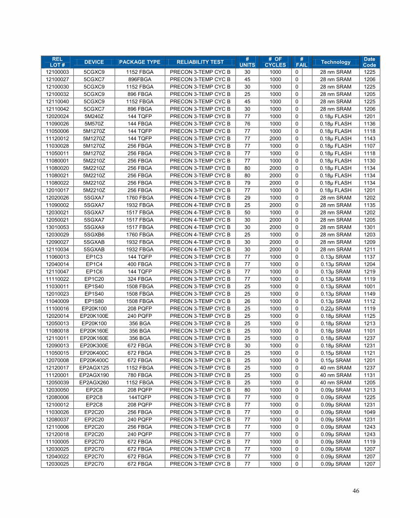
46
REL LOT # DEVICE PACKAGE TYPE RELIABILITY TEST #
UNITS # OF
CYCLES #
FAIL Technology Date Code
12100003 5CGXC9 1152 FBGA PRECON 3-TEMP CYC B 30 1000 0 28 nm SRAM 1225 12100027 5CGXC7 896FBGA PRECON 3-TEMP CYC B 45 1000 0 28 nm SRAM 1206 12100030 5CGXC9 1152 FBGA PRECON 3-TEMP CYC B 30 1000 0 28 nm SRAM 1225 12100032 5CGXC9 896 FBGA PRECON 3-TEMP CYC B 25 1000 0 28 nm SRAM 1205 12110040 5CGXC9 1152 FBGA PRECON 3-TEMP CYC B 45 1000 0 28 nm SRAM 1225 12110042 5CGXC7 896 FBGA PRECON 3-TEMP CYC B 30 1000 0 28 nm SRAM 1206 12020024 5M240Z 144 TQFP PRECON 3-TEMP CYC B 77 1000 0 0.18μ FLASH 1201 11090026 5M570Z 144 FBGA PRECON 3-TEMP CYC B 76 1000 0 0.18μ FLASH 1136 11050006 5M1270Z 144 TQFP PRECON 3-TEMP CYC B 77 1000 0 0.18μ FLASH 1118 11120012 5M1270Z 144 TQFP PRECON 3-TEMP CYC B 77 2000 0 0.18μ FLASH 1143 11030028 5M1270Z 256 FBGA PRECON 3-TEMP CYC B 77 1000 0 0.18μ FLASH 1107 11050011 5M1270Z 256 FBGA PRECON 3-TEMP CYC B 77 1000 0 0.18μ FLASH 1118 11080001 5M2210Z 256 FBGA PRECON 3-TEMP CYC B 77 1000 0 0.18μ FLASH 1130 11080020 5M2210Z 256 FBGA PRECON 3-TEMP CYC B 80 2000 0 0.18μ FLASH 1134 11080021 5M2210Z 256 FBGA PRECON 3-TEMP CYC B 80 2000 0 0.18μ FLASH 1134 11080022 5M2210Z 256 FBGA PRECON 3-TEMP CYC B 79 2000 0 0.18μ FLASH 1134 12010017 5M2210Z 256 FBGA PRECON 3-TEMP CYC B 77 1000 0 0.18μ FLASH 1201 12020026 5SGXA7 1760 FBGA PRECON 4-TEMP CYC B 29 1000 0 28 nm SRAM 1202 11090002 5SGXA7 1932 FBGA PRECON 4-TEMP CYC B 25 2000 0 28 nm SRAM 1135 12030021 5SGXA7 1517 FBGA PRECON 4-TEMP CYC B 50 1000 0 28 nm SRAM 1202 12050021 5SGXA7 1517 FBGA PRECON 4-TEMP CYC B 30 2000 0 28 nm SRAM 1205 13010053 5SGXA9 1517 FBGA PRECON 4-TEMP CYC B 30 2000 0 28 nm SRAM 1301 12030029 5SGXB6 1760 FBGA PRECON 4-TEMP CYC B 25 1000 0 28 nm SRAM 1203 12090027 5SGXAB 1932 FBGA PRECON 4-TEMP CYC B 30 2000 0 28 nm SRAM 1209 12110034 5SGXAB 1932 FBGA PRECON 4-TEMP CYC B 30 2000 0 28 nm SRAM 1211 11060013 EP1C3 144 TQFP PRECON 3-TEMP CYC B 77 1000 0 0.13µ SRAM 1137 12040014 EP1C4 400 FBGA PRECON 3-TEMP CYC B 77 1000 0 0.13µ SRAM 1204 12110047 EP1C6 144 TQFP PRECON 3-TEMP CYC B 77 1000 0 0.13µ SRAM 1219 11110022 EP1C20 324 FBGA PRECON 3-TEMP CYC B 77 1000 0 0.13µ SRAM 1119 11030011 EP1S40 1508 FBGA PRECON 3-TEMP CYC B 25 1000 0 0.13µ SRAM 1001 12010023 EP1S40 1508 FBGA PRECON 3-TEMP CYC B 25 1000 0 0.13µ SRAM 1149 11040009 EP1S80 1508 FBGA PRECON 3-TEMP CYC B 26 1000 0 0.13µ SRAM 1112 11100016 EP20K100 208 PQFP PRECON 3-TEMP CYC B 25 1000 0 0.22µ SRAM 1119 12020014 EP20K100E 240 PQFP PRECON 3-TEMP CYC B 25 1000 0 0.18µ SRAM 1125 12050013 EP20K100 356 BGA PRECON 3-TEMP CYC B 25 1000 0 0.18µ SRAM 1213 11080018 EP20K160E 356 BGA PRECON 3-TEMP CYC B 25 1000 0 0.18µ SRAM 1101 12110011 EP20K160E 356 BGA PRECON 3-TEMP CYC B 25 1000 0 0.18µ SRAM 1237 12090013 EP20K300E 672 FBGA PRECON 3-TEMP CYC B 30 1000 0 0.18µ SRAM 1231 11050015 EP20K400C 672 FBGA PRECON 3-TEMP CYC B 25 1000 0 0.15µ SRAM 1121 12070008 EP20K400C 672 FBGA PRECON 3-TEMP CYC B 25 1000 0 0.15µ SRAM 1201 12120017 EP2AGX125 1152 FBGA PRECON 3-TEMP CYC B 25 1000 0 40 nm SRAM 1237 11120001 EP2AGX190 780 FBGA PRECON 3-TEMP CYC B 25 1000 0 40 nm SRAM 1131 12050039 EP2AGX260 1152 FBGA PRECON 3-TEMP CYC B 25 1000 0 40 nm SRAM 1205 12030050 EP2C8 208 PQFP PRECON 3-TEMP CYC B 80 1000 0 0.09µ SRAM 1213 12080006 EP2C8 144TQFP PRECON 3-TEMP CYC B 77 1000 0 0.09µ SRAM 1225 12100012 EP2C8 208 PQFP PRECON 3-TEMP CYC B 77 1000 0 0.09µ SRAM 1231 11030026 EP2C20 256 FBGA PRECON 3-TEMP CYC B 77 1000 0 0.09µ SRAM 1049 12080037 EP2C20 240 PQFP PRECON 3-TEMP CYC B 77 1000 0 0.09µ SRAM 1231 12110006 EP2C20 256 FBGA PRECON 3-TEMP CYC B 77 1000 0 0.09µ SRAM 1243 12120018 EP2C20 240 PQFP PRECON 3-TEMP CYC B 77 1000 0 0.09µ SRAM 1243 11100005 EP2C70 672 FBGA PRECON 3-TEMP CYC B 77 1000 0 0.09µ SRAM 1119 12030025 EP2C70 672 FBGA PRECON 3-TEMP CYC B 77 1000 0 0.09µ SRAM 1207 12040022 EP2C70 672 FBGA PRECON 3-TEMP CYC B 77 1000 0 0.09µ SRAM 1207 12030025 EP2C70 672 FBGA PRECON 3-TEMP CYC B 77 1000 0 0.09µ SRAM 1207
47
REL LOT # DEVICE PACKAGE TYPE RELIABILITY TEST #
UNITS # OF
CYCLES #
FAIL Technology Date Code
12050035 EP2C70 672 FBGA PRECON 3-TEMP CYC B 77 1000 0 0.09µ SRAM 1207 12070001 EP2C70 672 FBGA PRECON 3-TEMP CYC B 77 1000 0 0.09µ SRAM 1207 12090011 EP2C70 672 FBGA PRECON 3-TEMP CYC B 77 1000 0 0.09µ SRAM 1219 11060011 EP2S90 1020 FBGA PRECON 3-TEMP CYC B 25 1000 0 0.09µ SRAM 1125 12040010 EP2S90 1508 FBGA PRECON 3-TEMP CYC B 25 1000 0 0.09µ SRAM 1207 12090020 EP2S90 1508 FBGA PRECON 3-TEMP CYC B 25 1000 0 0.09µ SRAM 1213 11120011 EP2S130 1508 FBGA PRECON 3-TEMP CYC B 25 1000 0 0.09µ SRAM 1119 12110012 EP3C25 144 EQFP PRECON 3-TEMP CYC B 77 1000 0 60 nm SRAM 1237 11060006 EP3C40 240 PQFP PRECON 3-TEMP CYC B 77 1000 0 60 nm SRAM 1113 11040001 EP3C80 484 UBGA PRECON 3-TEMP CYC B 80 1000 0 60 nm SRAM 1127 11050010 EP3C80 484 UBGA PRECON 3-TEMP CYC B 78 1000 0 60 nm SRAM 1101 11040010 EP3C120 780 FBGA PRECON 3-TEMP CYC B 77 1000 0 60 nm SRAM 1117 11040013 EP3C120 780 FBGA PRECON 3-TEMP CYC B 77 1000 0 60 nm SRAM 1117 11060010 EP3C120 780 FBGA PRECON 3-TEMP CYC B 30 1000 0 60 nm SRAM 1124 12040030 EP3C120 780 FBGA PRECON 3-TEMP CYC B 77 1000 0 60 nm SRAM 1213 12060015 EP3C120 780 FBGA PRECON 3-TEMP CYC B 77 1000 0 60 nm SRAM 1222 12040011 EP3C120 780 FBGA PRECON 3-TEMP CYC B 24 2000 0 60 nm SRAM 1214 11030015 EP3SE50 780 FBGA PRECON 3-TEMP CYC B 25 1000 0 65 nm SRAM 1043 12100005 EP3SE50 780 FBGA PRECON 3-TEMP CYC B 25 1000 0 65 nm SRAM 1237 11070014 EP3SL50 780 FBGA PRECON 3-TEMP CYC B 25 1000 0 65 nm SRAM 1112 11100002 EP3SL150 1152 FBGA PRECON 3-TEMP CYC B 25 1000 0 65 nm SRAM 1119 12070022 EP3SL150 1152 FBGA PRECON 3-TEMP CYC B 25 1000 0 65 nm SRAM 1225 11080004 EP3SL200 1152 FBGA PRECON 3-TEMP CYC B 25 1000 0 65 nm SRAM 1049 12010021 EP3SL200 1152 FBGA PRECON 3-TEMP CYC B 25 1000 0 65 nm SRAM 1146 11030010 EP4CGX15 148 QFN PRECON 3-TEMP CYC B 77 1000 0 60 nm SRAM 1101 11100015 EP4CGX15 148 QFN PRECON 3-TEMP CYC B 77 1000 0 60 nm SRAM 1131 12080036 EP4CGX15 148 QFN PRECON 3-TEMP CYC B 77 1000 0 60 nm SRAM 1231 11070025 EP4CGX150 896 FBGA PRECON 3-TEMP CYC B 77 1000 0 60 nm SRAM 1119 12020033 EP4CGX150 896 FBGA PRECON 3-TEMP CYC B 77 1000 0 60 nm SRAM 1201 11010007 EP4SGX230 1517 FBGA PRECON 3-TEMP CYC B 25 1000 0 40 nm SRAM 1101 11030012 EP4SGX230 1517 FBGA PRECON 3-TEMP CYC B 24 1000 0 40 nm SRAM 1108 11120033 EP4SGX230 1517 FBGA PRECON 3-TEMP CYC B 25 1000 0 40 nm SRAM 1137 12080033 EP4SGX230 1517 FBGA PRECON 3-TEMP CYC B 25 1000 0 40 nm SRAM 1208 11010001 EP4SGX530 1517 HBGA PRECON 4-TEMP CYC B 25 1000 0 40 nm SRAM 1101 12050041 EP4SGX530 1517HBGA PRECON 3-TEMP CYC B 25 1000 0 40 nm SRAM 1205 11090028 EPC1 20 PLCC PRECON 3-TEMP CYC B 45 1000 0 0.5µ EPROM 1127 12080001 EPC1 20 PLCC PRECON 3-TEMP CYC B 45 1000 0 0.5µ EPROM 1230 12030019 EPC1441 20 PLCC PRECON 3-TEMP CYC B 45 1000 0 0.5µ EPROM 1207 11080010 EPC2 20 PLCC PRECON 3-TEMP CYC B 45 1000 0 0.4m FLASH 1113 12020028 EPC2 20 PLCC PRECON 3-TEMP CYC B 45 1000 0 0.4m FLASH 1204 11120037 EPC16 100 PQFP PRECON 3-TEMP CYC B 45 1000 0 0.35m FLASH 1142 12100009 EPC16 88 UBGA PRECON 3-TEMP CYC B 45 1000 0 0.35m FLASH 1231 12030020 EPF10K50A 356 FBGA PRECON 3-TEMP CYC B 25 1000 0 0.3µ SRAM 1201 11040014 EPF10K70 240 RQFP PRECON 3-TEMP CYC B 25 1000 0 0.42µ SRAM 1107 12090012 EPF10K70 240 RQFP PRECON 3-TEMP CYC B 25 1000 0 0.42µ SRAM 1231 11070013 EPF10K100A 484 FBGA PRECON 3-TEMP CYC B 25 1000 0 0.3µ SRAM 1137 12030028 EPF10K100E 208 PQFP PRECON 3-TEMP CYC B 25 1000 0 0.22µ SRAM 1143 11110023 EPF10K100E 356 BGA PRECON 3-TEMP CYC B 25 1000 0 0.22µ SRAM 1131 11030014 EPF6016 208 PQFP PRECON 3-TEMP CYC B 25 1000 0 0.42µ SRAM 1101 12090021 EPF6016 208 PQFP PRECON 3-TEMP CYC B 25 1000 0 0.42µ SRAM 1225 11030013 EPM240Z 100 MBGA PRECON 3-TEMP CYC B 77 1000 0 0.18μ FLASH 1101 12120006 EPM240 100 MBGA PRECON 3-TEMP CYC B 77 1000 0 0.18μ FLASH 1243 11030018 EPM570 100 TQFP PRECON 3-TEMP CYC B 24 1000 0 0.18μ FLASH 1112 11070012 EPM570 100 TQFP PRECON 3-TEMP CYC B 78 1000 0 0.18μ FLASH 1128
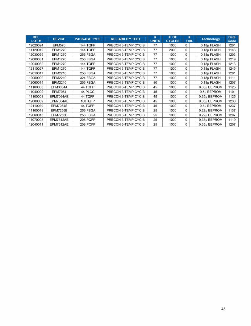
48
REL LOT # DEVICE PACKAGE TYPE RELIABILITY TEST #
UNITS # OF
CYCLES #
FAIL Technology Date Code
12020024 EPM570 144 TQFP PRECON 3-TEMP CYC B 77 1000 0 0.18μ FLASH 1201 11120012 EPM1270 144 TQFP PRECON 3-TEMP CYC B 77 2000 0 0.18μ FLASH 1143 12030039 EPM1270 256 FBGA PRECON 3-TEMP CYC B 77 1000 0 0.18μ FLASH 1203 12080031 EPM1270 256 FBGA PRECON 3-TEMP CYC B 77 1000 0 0.18μ FLASH 1219 12040032 EPM1270 144 TQFP PRECON 3-TEMP CYC B 77 1000 0 0.18μ FLASH 1213 12110027 EPM1270 144 TQFP PRECON 3-TEMP CYC B 77 1000 0 0.18μ FLASH 1245 12010017 EPM2210 256 FBGA PRECON 3-TEMP CYC B 77 1000 0 0.18µ FLASH 1201 12050002 EPM2210 324 FBGA PRECON 3-TEMP CYC B 77 1000 0 0.18µ FLASH 1111 12060014 EPM2210 256 FBGA PRECON 3-TEMP CYC B 80 1000 0 0.18µ FLASH 1207 11100003 EPM3064A 44 TQFP PRECON 3-TEMP CYC B 45 1000 0 0.35µ EEPROM 1125 11040002 EPM7064 44 PLCC PRECON 3-TEMP CYC B 45 1000 0 0.5µ EEPROM 1101 11100003 EPM7064AE 44 TQFP PRECON 3-TEMP CYC B 45 1000 0 0.35µ EEPROM 1125 12080009 EPM7064AE 100TQFP PRECON 3-TEMP CYC B 45 1000 0 0.35µ EEPROM 1230 12110039 EPM7064S 44 TQFP PRECON 3-TEMP CYC B 45 1000 0 0.5µ EEPROM 1237 11100018 EPM7256B 256 FBGA PRECON 3-TEMP CYC B 25 1000 0 0.22µ EEPROM 1137 12060013 EPM7256B 256 FBGA PRECON 3-TEMP CYC B 25 1000 0 0.22µ EEPROM 1207 11070008 EPM7512AE 208 PQFP PRECON 3-TEMP CYC B 25 1000 0 0.35µ EEPROM 1119 12040011 EPM7512AE 208 PQFP PRECON 3-TEMP CYC B 25 1000 0 0.35µ EEPROM 1207
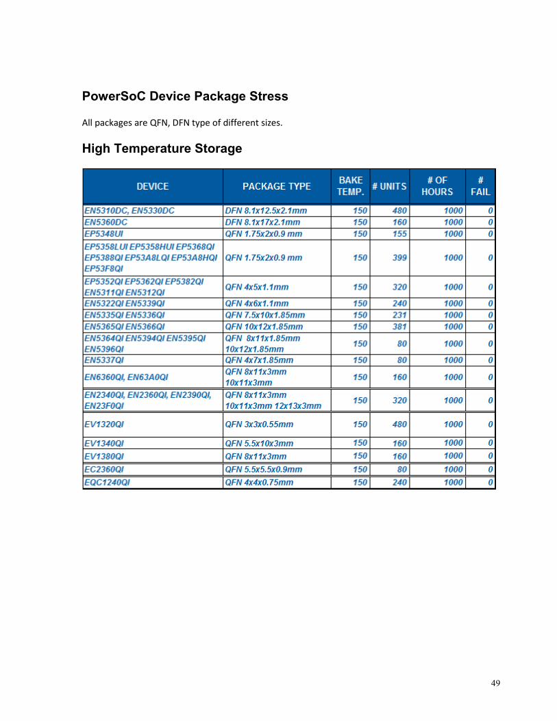
49
PowerSoC Device Package Stress All packages are QFN, DFN type of different sizes.
High Temperature Storage
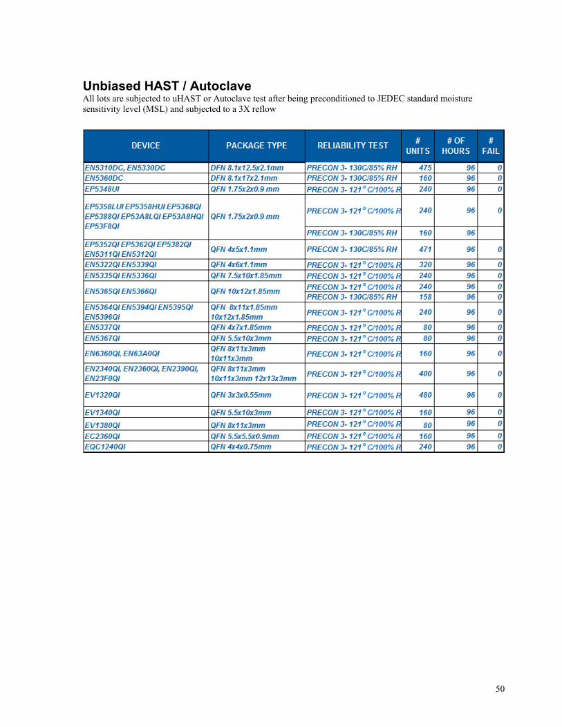
50
Unbiased HAST / Autoclave All lots are subjected to uHAST or Autoclave test after being preconditioned to JEDEC standard moisture sensitivity level (MSL) and subjected to a 3X reflow

51
Temperature Humidity Test All lots are subjected to Biased Humidity test after being preconditioned to JEDEC standard moisture sensitivity level (MSL) and subjected to a 3X reflow

52
Temperature Cycling: (Conditions C: –65°C to +150°C 500 cycles) All lots are subjected to T/C after being preconditioned to JEDEC standard moisture sensitivity level (MSL) and subjected to a 3X reflow.

53
Solder Joint Reliability Reference: IPC9701 Solder Joint Reliability is measured by temperature cycling devices on a printed circuit board from 0°C to 100°C. The number of cycle can go to up to 6000 cycles to detect first fail. Tin-Lead (Sn-Pb) Solder Ball
Package Substrate pad size Pitch Technology heat sink Die Size
(mm) MTTF
(Cycles) Cycles to 0.1%
fails (Extrapolated)
F1681 0.55 mm 1.0 mm Molded Flip Chip + 8 layer build-up BT None 18 * 22
(N40 ELK die) 3656 2958
F1932 0.55 mm 1.0 mm Flip Chip + 8 layer build-up BT
1mm FTSPL 31x26 4021 3136
U88 0.4 mm 0.8 mm Wire-bonded Stacked Die + 2L FR4 substrate None 6.9 * 4.6 4068 3162
E144 NA 0.5mm lead frame + ground pad None 5.12 * 5.21 0 fail to 6000 0 fails to 6000
QFN148 NA 0.5mm lead frame + ground pad None 5.12 * 5.21 2839 2119
F256 0.45mm 1.0mm low k die + Wire Bond + 4 Layer BT None 5.80*6.22 4798 3775
F256 0.45mm 1.0mm low k die + Wire Bond + 4 Layer BT None 5.80*6.22 5058 3236
F256 0.45mm 1.0mm low k die + Wire Bond + 4 Layer BT None 5.80*6.22 4194 2161
F256 0.45 mm 1.0 mm Wire Bond + 2 Layer BT None 8.8 * 7.9 4437 3687
F256 thin outline 0.45 mm 1.0 mm low k die + Wire Bond +
4 Layer BT None 7.68 * 6.81 3574 2888
F256 0.45mm 1.0mm Wire bond + 2Layer BT None 5.46 x 5.85 4437 3713
B356 0.58 mm 1.27 mm
Wire Bond + 2 Layer BT None 9 * 9.8 0 fail to 5000 0 fails to 5000
U358 0.4mm 0.8mm Lid-less Flip-Chip + 4L build up BT None 10.11*10 2777 2740
U484 0.4mm 0.8mm low k die + Wire Bond + 4 Layer BT None 8.4 * 8.03 0 fail to 5000 0 fails to 5000
B652 0.58 mm 1.27 mm
Wire bond + 1 Layer Tape Cu 17.01 * 15.38 0 fail to 5000 0 fails to 5000
B724 0.55 mm 1.27 mm
Flip Chip + 6 layer build-up BT 2 pc Cu 18.1 * 13.4 0 fail to 2800 0 fails to 2800
F484 0.45 mm 1.0 mm Wire bond + 2 layer BT None 11.5 * 11.5 6534 3408
F672 0.45 mm 1.0 mm Wire Bond + 4 Layer BT None 11.19*11.12 5601 4448
F672 0.45 mm 1.0 mm Wire Bond + 4 Layer BT None 16 * 11.8 0 fail at 5200 0 fails at 5200
F672 0.45 mm 1.0 mm Wire Bond + 4 Layer BT None 16 * 11.8 0 fail at 5400 0 fails at 5400
F672 0.45mm 1.0mm Low K die + Wire Bond + 4 Layer BT None 8.4 * 8.03 0 fail to 5400 0 fails to 5400
F672 0.55 mm 1.0 mm Flip Chip + 8 layer build-up BT AlSiC 19.1 * 16.5 4419 3284
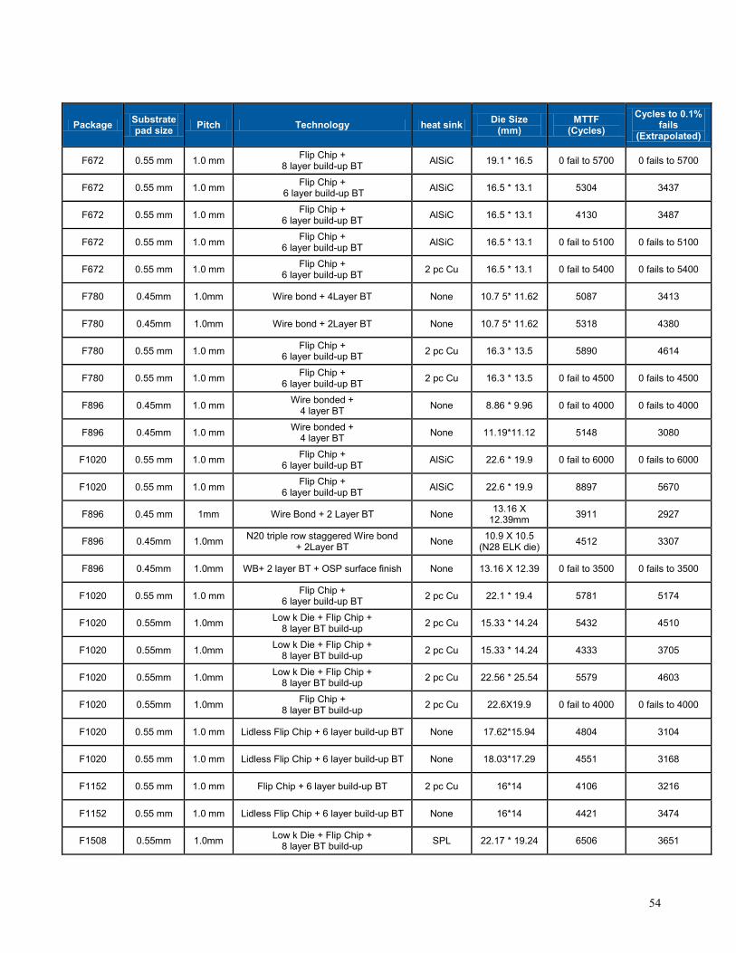
54
Package Substrate pad size Pitch Technology heat sink Die Size
(mm) MTTF
(Cycles) Cycles to 0.1%
fails (Extrapolated)
F672 0.55 mm 1.0 mm Flip Chip + 8 layer build-up BT AlSiC 19.1 * 16.5 0 fail to 5700 0 fails to 5700
F672 0.55 mm 1.0 mm Flip Chip + 6 layer build-up BT AlSiC 16.5 * 13.1 5304 3437
F672 0.55 mm 1.0 mm Flip Chip + 6 layer build-up BT AlSiC 16.5 * 13.1 4130 3487
F672 0.55 mm 1.0 mm Flip Chip + 6 layer build-up BT AlSiC 16.5 * 13.1 0 fail to 5100 0 fails to 5100
F672 0.55 mm 1.0 mm Flip Chip + 6 layer build-up BT 2 pc Cu 16.5 * 13.1 0 fail to 5400 0 fails to 5400
F780 0.45mm 1.0mm Wire bond + 4Layer BT None 10.7 5* 11.62 5087 3413
F780 0.45mm 1.0mm Wire bond + 2Layer BT None 10.7 5* 11.62 5318 4380
F780 0.55 mm 1.0 mm Flip Chip + 6 layer build-up BT 2 pc Cu 16.3 * 13.5 5890 4614
F780 0.55 mm 1.0 mm Flip Chip + 6 layer build-up BT 2 pc Cu 16.3 * 13.5 0 fail to 4500 0 fails to 4500
F896 0.45mm 1.0 mm Wire bonded + 4 layer BT None 8.86 * 9.96 0 fail to 4000 0 fails to 4000
F896 0.45mm 1.0 mm Wire bonded + 4 layer BT None 11.19*11.12 5148 3080
F1020 0.55 mm 1.0 mm Flip Chip + 6 layer build-up BT AlSiC 22.6 * 19.9 0 fail to 6000 0 fails to 6000
F1020 0.55 mm 1.0 mm Flip Chip + 6 layer build-up BT AlSiC 22.6 * 19.9 8897 5670
F896 0.45 mm 1mm Wire Bond + 2 Layer BT None 13.16 X 12.39mm 3911 2927
F896 0.45mm 1.0mm N20 triple row staggered Wire bond + 2Layer BT None 10.9 X 10.5
(N28 ELK die) 4512 3307
F896 0.45mm 1.0mm WB+ 2 layer BT + OSP surface finish None 13.16 X 12.39 0 fail to 3500 0 fails to 3500
F1020 0.55 mm 1.0 mm Flip Chip + 6 layer build-up BT 2 pc Cu 22.1 * 19.4 5781 5174
F1020 0.55mm 1.0mm Low k Die + Flip Chip + 8 layer BT build-up 2 pc Cu 15.33 * 14.24 5432 4510
F1020 0.55mm 1.0mm Low k Die + Flip Chip + 8 layer BT build-up 2 pc Cu 15.33 * 14.24 4333 3705
F1020 0.55mm 1.0mm Low k Die + Flip Chip + 8 layer BT build-up 2 pc Cu 22.56 * 25.54 5579 4603
F1020 0.55mm 1.0mm Flip Chip + 8 layer BT build-up 2 pc Cu 22.6X19.9 0 fail to 4000 0 fails to 4000
F1020 0.55 mm 1.0 mm Lidless Flip Chip + 6 layer build-up BT None 17.62*15.94 4804 3104
F1020 0.55 mm 1.0 mm Lidless Flip Chip + 6 layer build-up BT None 18.03*17.29 4551 3168
F1152 0.55 mm 1.0 mm Flip Chip + 6 layer build-up BT 2 pc Cu 16*14 4106 3216
F1152 0.55 mm 1.0 mm Lidless Flip Chip + 6 layer build-up BT None 16*14 4421 3474
F1508 0.55mm 1.0mm Low k Die + Flip Chip + 8 layer BT build-up SPL 22.17 * 19.24 6506 3651

55
Package Substrate pad size Pitch Technology heat sink Die Size
(mm) MTTF
(Cycles) Cycles to 0.1%
fails (Extrapolated)
F1508 0.55 mm 1.0 mm Flip Chip + 6 layer build-up BT 2 pc Cu 23.9 * 23.3 4233 2694
F1508 0.55 mm 1.0 mm Flip Chip + 6 layer build-up BT 2 pc Cu 23.9 * 23.3 3074 2040
F1508 0.55 mm 1.0 mm Flip Chip + 6 layer build-up BT SPL 23.9 * 23.3 4797 3182
F1517 0.55 mm 1.0 mm Flip Chip + 14 layer build-up BT 2 pc Cu 25.6 * 26.5
(N40 ELK die) 4497 3564
F1517 0.55 mm 1.0 mm Flip Chip + 14 layer build-up BT SPL 25.6 * 26.5
(N40 ELK die) 4733 4100
F1681 0.55 mm 1.0 mm Flip Chip + 8 layer build-up BT SPL 18 * 22 (N40 ELK die) 0 fail to 4890 0 fail to 4890
F1760 0.55 mm 1.0 mm Flip Chip + 12 layer build-up BT 2 pc Cu 20.0 * 20.0
(N40 ELK die) 3541 2572
F1760 0.55 mm 1.0 mm Flip Chip + 8 layer build-up BT SPL
25.5 * 26.5 (N28 ELK
die) 3703 3296
F1932 0.55 mm 1.0 mm Flip Chip + 8 layer build-up BT 2 pc Cu 25.6 * 26.5
(N28 ELK die) 3552 2932
Lead Free Solder Ball
Package Substrate pad size Pitch Technology heat sink Die Size
(mm) MTTF
(cycles) Cycles to 0.1%
fails (Extrapolated)
F1152 0.45mm 1.0mm Wire bonded + 4 layer BT None 13.2*13.53 0 fail to 4800 0 fail to 4800
F1932 0.55 mm 1.0mm Flip Chip + 8 layer build-up BT 1 mm FTSPL 31*26 0 fail to 7000 0 fail to 7000
M100 0.3 mm 0.5 mm Wire Bond + 2 Layer BT None 3.2 * 3.2 0 fail to 6000 0 fail to 6000
M256 0.3 mm 0.5 mm Wire Bond + 4 Layer BT None 3.9 * 3.9 0 fail to 6000 0 fail to 6000
U88 0.4 mm 0.8 mm Wire-bonded Stacked Die + 2L FR4 substrate None 6.9 * 4.6 0 fail to 6000 0 fail to 6000
T144 N/A 0.5 mm lead frame N/A 4.9*6.0 0 fail to 5500 0 fail to 5500
E144 NA 0.5mm lead frame + ground pad None 5.12 * 5.21 0 fail to 6000 0 fail to 6000
QFN148 NA 0.5mm lead frame + ground pad None 5.12 * 5.21 2938 2511
F256 thin
outline 0.45 mm 1.0 mm Wire Bond +
4 Layer BT None 7.68 * 6.81 0 fail to 5000 0 fail to 5000
F256 0.45mm 1.0mm low k die + Wire Bond + 4 Layer BT None 5.80*6.22 0 fail to 6000 0 fail to 6000
F256 0.45mm 1.0mm Wire bond + 2Layer BT None 5.46 x 5.85 0 fail to 6000 0 fail to 6000
Q240 N/A 0.5 mm lead frame N/A 8.0*7.9 0 fail to 6000 0 fails to 6000
U358 0.4mm 0.8mm Lid-less Flip-Chip + 4 Layer build up BT None 10.11*10 0 fail to 6000 0 fails to 6000

56
Package Substrate pad size Pitch Technology heat sink Die Size
(mm) MTTF
(cycles) Cycles to 0.1%
fails (Extrapolated)
U484 0.4mm 0.8mm low k die + Wire Bond + 4 Layer BT None 8.4 * 8.03 0 fail to 3500 0 fail to 3500
F484 0.45mm 1.0 mm Wire-bonded + 4 layer BT None 10.8 * 8.8 0 fail to 6000 0 fail to 6000
F672 0.45 mm 1.0 mm Wire Bond + 4 Layer BT None 11.19*11.12 0 fail to 6000 0 fail to 6000
F780 0.55 mm 1.0 mm Flip Chip + 6 layer build-up BT 2 pc Cu 16.3 * 13.5 0 fail to 5000 0 fail to 5000
F896 0.45mm 1.0 mm Wire-bonded + 4 layer BT None 8.86 * 9.96 0 fail to 4000 0 fail to 4000
F896 0.45mm 1.0 mm Wire bonded + 4 layer BT None 11.19*11.12 0 fail to 6000 0 fail to 6000
F896 0.45mm 1.0mm N20 triple row staggered Wire bond + 2Layer BT None 10.9 X 10.5
(N28 ELK) 0 fail to 6000 0 fail to 6000
M1019 0.3mm 0.5mm Lid-less Flip-Chip + 3-2-3 build up substrate None 10.16*10.52 0 fail to 6000 0 fail to 6000
F1020 0.55 mm 1.0 mm Flip Chip + 6 layer build-up BT 2 pc Cu 22.6 * 19.9 0 fail to 5887 0 fail to 5887
F1020 0.55 mm 1.0 mm Flip Chip + 6 layer build-up BT SPL 17.62*15.94 0 fail to 6000 0 fail to 6000
F1020 0.55 mm 1.0 mm Lidless Flip Chip + 6 layer build-up BT None 17.62*15.94 0 fail to 6000 0 fail to 6000
F1020 0.55 mm 1.0 mm Flip Chip + 6 layer build-up BT SPL 18.03*17.29 0 fail to 6000 0 fail to 6000
F1020 0.55 mm 1.0 mm Lidless Flip Chip + 6 layer build-up BT None 18.03*17.29 0 fail to 6000 0 fail to 6000
F1508 0.55 mm 1.0 mm Flip Chip + 6 layer build-up BT 2 pc Cu 23.9 * 23.3 0 fail to 6000 0 fail to 6000
F1681 0.55 mm 1.0 mm Molded Flip Chip + 8 layer build-up BT None 18 * 22 (N40 ELK die) 0 fail to 7000 0 fail to 7000
F1760 0.55 mm 1.0 mm Flip Chip + 8 layer build-up BT SPL 25 * 26 (N28 ELK die) 0 fail to 7000 0 fail to 7000
F1932 0.55 mm 1.0 mm Flip Chip + 8 layer build-up BT SPL 25 * 26 (N28 ELK die) 0 fail to 6000 0 fail to 6000
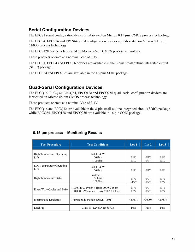
57
Serial Configuration Devices The EPCS1 serial configuration device is fabricated on Micron 0.15 μm. CMOS process technology.
The EPCS4, EPCS16 and EPCS64 serial configuration devices are fabricated on Micron 0.11 μm CMOS process technology.
The EPCS128 device is fabricated on Micron 65nm CMOS process technology.
These products operate at a nominal Vcc of 3.3V.
The EPCS1, EPCS4 and EPCS16 devices are available in the 8-pins small outline integrated circuit (SOIC) package.
The EPCS64 and EPCS128 are available in the 16-pins SOIC package.
Quad-Serial Configuration Devices The EPCQ16, EPCQ32, EPCQ64, EPCQ128 and EPCQ256 quad- serial configuration devices are fabricated on Micron 65 nm CMOS process technology.
These products operate at a nominal Vcc of 3.3V.
The EPCQ16 and EPCQ32 are available in the 8-pin small outline integrated circuit (SOIC) package while EPCQ64, EPCQ128 and EPCQ256 are available in 16-pin SOIC package.
0.15 μm process – Monitoring Results
Test Procedure Test Conditions Lot 1 Lot 2 Lot 3
High Temperature Operating Life
140°C, 4.2V 504hrs
1008hrs 0/80 0/80
0/77 0/77
0/80 0/80
Low Temperature Operating Life –40°C, 4.2V
504hrs 0/80 0/77 0/80
High Temperature Bake 200°C,
500hrs 1000hrs
0/77 0/77
0/77 0/77
0/77 0/77
Erase/Write Cycles and Bake 10,000 E/W cycles + Bake 200°C, 48hrs 100,000 E/W cycles + Bake 200°C, 48hrs
0/77 0/77
0/77 0/77
0/77 0/77
Electrostatic Discharge Human body model: 1.5kΩ, 100pF >2000V >2000V >2000V
Latch-up Class II - Level A (at 85°C) Pass Pass Pass

58
0.11 μm process – Monitoring Results
Test Procedure Test Conditions Lot 1 Lot 2 Lot 3
High Temperature Operating Life
140°C, 4.2V 168 hrs 500 hrs
0/77 0/77 0/77 0/77
0/77 0/77
Low Temperature Operating Life –40°C, 4.2V
168 hrs 0/15 0/15 0/15
High Temperature Bake 250°C,
168 hrs 500 hrs 0/77 0/77 0/77 0/77
0/77 0/77
Erase/Write Cycles and Bake 10,000 E/W cycles
100,000 E/W cycles + Bake 250°C, 168 hrs
0/77 0/77 0/77
0/77 0/77 0/77
0/77 0/77 0/77
Electrostatic Discharge Human body model: 1.5kΩ, 100pF Machine Model: 0 Ω, 200pF
>2000V >200 V
>2000V > 200 V
>2000V >200 V
Latch-up Class II - Level A (at 150°C) Pass Pass Pass
65 nm process – Monitoring Results
Test Procedure Test Conditions Hours or cycles (Failures/Devices)
Failure/Sampling
ELFR 125°C Read 168 Hours 0/4733
NVM cycling Room Temperature 1000 cycles 0/731
Temperature Cycle -55°C for 15mn, 125°C for 15mn, air to air 500 cycles 1000 cycles
0/1252 0/1252
High Temperature Storage 150°C, no bias 504 Hours
1008 Hours 0/1509 0/1509
Unbiased HAST 130°C, 85% RH 96 Hours 0/1511

59
i JEDEC publication, JEP122-E, “Failure Mechanisms and Models for Semiconductor Devices” pp29-
31, Table 1. http://www.jedec.org/download/search/jep122a.pdf ii Microsoft Excel 5.0 statistical functions, Inverse Chi-Squared Distribution, variables are degrees of
freedom and Confidence Level.