regulating pulse width modulator datasheet - ti.com · regulating pulse width modulator ... •...
TRANSCRIPT
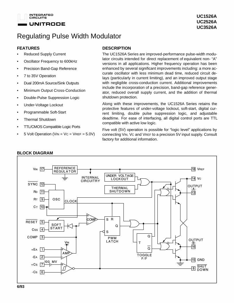
BLOCK DIAGRAM
UC1526AUC2526AUC3526A
Regulating Pulse Width Modulator
FEATURES• Reduced Supply Current
• Oscillator Frequency to 600kHz
• Precision Band-Gap Reference
• 7 to 35V Operation
• Dual 200mA Source/Sink Outputs
• Minimum Output Cross-Conduction
• Double-Pulse Suppression Logic
• Under-Voltage Lockout
• Programmable Soft-Start
• Thermal Shutdown
• TTL/CMOS Compatible Logic Ports
• 5 Volt Operation (VIN = VC = VREF = 5.0V)
DESCRIPTIONThe UC1526A Series are improved-performance pulse-width modu-lator circuits intended for direct replacement of equivalent non- “A”versions in all applications. Higher frequency operation has beenenhanced by several significant improvements including: a more ac-curate oscillator with less minimum dead time, reduced circuit de-lays (particularly in current limiting), and an improved output stagewith negligible cross-conduction current. Additional improvementsinclude the incorporation of a precision, band-gap reference gener-ator, reduced overall supply current, and the addition of thermalshutdown protection.
Along with these improvements, the UC1526A Series retains theprotective features of under-voltage lockout, soft-start, digital cur-rent limiting, double pulse suppression logic, and adjustabledeadtime. For ease of interfacing, all digital control ports are TTLcompatible with active low logic.
Five volt (5V) operation is possible for “logic level” applications byconnecting VIN, VC and VREF to a precision 5V input supply. Consultfactory for additional information.
6/93
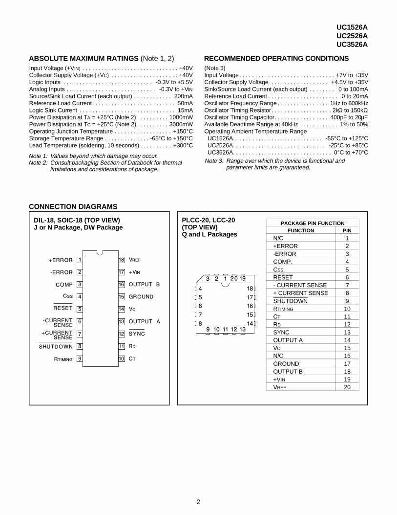
RECOMMENDED OPERATING CONDITIONS (Note 3)Input Voltage. . . . . . . . . . . . . . . . . . . . . . . . . . . . . . +7V to +35VCollector Supply Voltage . . . . . . . . . . . . . . . . . . +4.5V to +35VSink/Source Load Current (each output) . . . . . . . . 0 to 100mAReference Load Current . . . . . . . . . . . . . . . . . . . . . . 0 to 20mAOscillator Frequency Range . . . . . . . . . . . . . . . . 1Hz to 600kHzOscillator Timing Resistor. . . . . . . . . . . . . . . . . . . 2kΩ to 150kΩOscillator Timing Capacitor. . . . . . . . . . . . . . . . . 400pF to 20µFAvailable Deadtime Range at 40kHz . . . . . . . . . . . . 1% to 50%Operating Ambient Temperature Range UC1526A. . . . . . . . . . . . . . . . . . . . . . . . . . . . -55°C to +125°C UC2526A. . . . . . . . . . . . . . . . . . . . . . . . . . . . . -25°C to +85°C UC3526A. . . . . . . . . . . . . . . . . . . . . . . . . . . . . . . 0°C to +70°C
ABSOLUTE MAXIMUM RATINGS (Note 1, 2)Input Voltage (+VIN) . . . . . . . . . . . . . . . . . . . . . . . . . . . . . . +40VCollector Supply Voltage (+VC) . . . . . . . . . . . . . . . . . . . . . +40VLogic Inputs . . . . . . . . . . . . . . . . . . . . . . . . . . . . -0.3V to +5.5VAnalog Inputs . . . . . . . . . . . . . . . . . . . . . . . . . . . . -0.3V to +VIN
Source/Sink Load Current (each output) . . . . . . . . . . . . 200mAReference Load Current . . . . . . . . . . . . . . . . . . . . . . . . . . 50mALogic Sink Current . . . . . . . . . . . . . . . . . . . . . . . . . . . . . . 15mAPower Dissipation at TA = +25°C (Note 2) . . . . . . . . . 1000mWPower Dissipation at TC = +25°C (Note 2) . . . . . . . . . . 3000mWOperating Junction Temperature . . . . . . . . . . . . . . . . . . +150°CStorage Temperature Range . . . . . . . . . . . . . . -65°C to +150°CLead Temperature (soldering, 10 seconds) . . . . . . . . . . +300°C
CONNECTION DIAGRAMS
PACKAGE PIN FUNCTIONFUNCTION PIN
N/C 1+ERROR 2-ERROR 3COMP. 4CSS 5RESET 6- CURRENT SENSE 7+ CURRENT SENSE 8SHUTDOWN 9RTIMING 10CT 11RD 12SYNC 13OUTPUT A 14VC 15N/C 16GROUND 17OUTPUT B 18+VIN 19VREF 20
PLCC-20, LCC-20 (TOP VIEW) Q and L Packages
DIL-18, SOIC-18 (TOP VIEW)J or N Package, DW Package
Note 1: Values beyond which damage may occur.Note 2: Consult packaging Section of Databook for thermal
limitations and considerations of package.Note 3: Range over which the device is functional and
parameter limits are guaranteed.
UC1526AUC2526AUC3526A
2
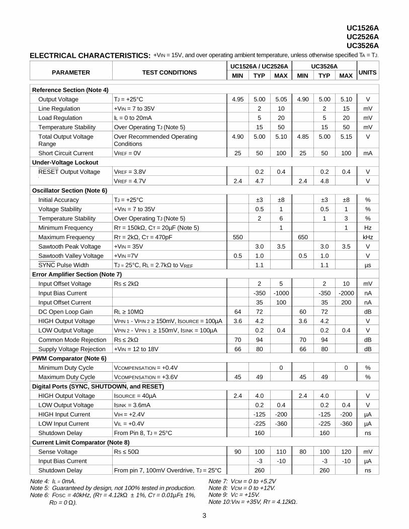
PARAMETER TEST CONDITIONSUC1526A / UC2526A UC3526A
UNITSMIN TYP MAX MIN TYP MAX
Reference Section (Note 4)
Output Voltage TJ = +25°C 4.95 5.00 5.05 4.90 5.00 5.10 V
Line Regulation +VIN = 7 to 35V 2 10 2 15 mV
Load Regulation IL = 0 to 20mA 5 20 5 20 mV
Temperature Stability Over Operating TJ (Note 5) 15 50 15 50 mV
Total Output VoltageRange
Over Recommended OperatingConditions
4.90 5.00 5.10 4.85 5.00 5.15 V
Short Circuit Current VREF = 0V 25 50 100 25 50 100 mA
Under-Voltage Lockout
RESET Output Voltage VREF = 3.8V 0.2 0.4 0.2 0.4 V
VREF = 4.7V 2.4 4.7 2.4 4.8 V
Oscillator Section (Note 6)
Initial Accuracy TJ = +25°C ±3 ±8 ±3 ±8 %
Voltage Stability +VIN = 7 to 35V 0.5 1 0.5 1 %
Temperature Stability Over Operating TJ (Note 5) 2 6 1 3 %
Minimum Frequency RT = 150kΩ, CT = 20µF (Note 5) 1 1 Hz
Maximum Frequency RT = 2kΩ, CT = 470pF 550 650 kHz
Sawtooth Peak Voltage +VIN = 35V 3.0 3.5 3.0 3.5 V
Sawtooth Valley Voltage +VIN =7V 0.5 1.0 0.5 1.0 V
SYNC Pulse Width TJ = 25°C, RL = 2.7kΩ to VREF 1.1 1.1 µs
Error Amplifier Section (Note 7)
Input Offset Voltage RS ≤ 2kΩ 2 5 2 10 mV
Input Bias Current -350 -1000 -350 -2000 nA
Input Offset Current 35 100 35 200 nA
DC Open Loop Gain RL ≥ 10MΩ 64 72 60 72 dB
HIGH Output Voltage VPIN 1 - VPIN 2 ≥ 150mV, ISOURCE = 100µA 3.6 4.2 3.6 4.2 V
LOW Output Voltage VPIN 2 - VPIN 1 ≥ 150mV, ISINK = 100µA 0.2 0.4 0.2 0.4 V
Common Mode Rejection RS ≤ 2kΩ 70 94 70 94 dB
Supply Voltage Rejection +VIN = 12 to 18V 66 80 66 80 dB
PWM Comparator (Note 6)
Minimum Duty Cycle VCOMPENSATION = +0.4V 0 0 %
Maximum Duty Cycle VCOMPENSATION = +3.6V 45 49 45 49 %
Digital Ports ( SYNC, SHUTDOWN, and RESET)
HIGH Output Voltage ISOURCE = 40µA 2.4 4.0 2.4 4.0 V
LOW Output Voltage ISINK = 3.6mA 0.2 0.4 0.2 0.4 V
HIGH Input Current VIH = +2.4V -125 -200 -125 -200 µA
LOW Input Current VIL = +0.4V -225 -360 -225 -360 µA
Shutdown Delay From Pin 8, TJ = 25°C 160 160 ns
Current Limit Comparator (Note 8)
Sense Voltage RS ≤ 50Ω 90 100 110 80 100 120 mV
Input Bias Current -3 -10 -3 -10 µA
Shutdown Delay From pin 7, 100mV Overdrive, TJ = 25°C 260 260 ns
+VIN = 15V, and over operating ambient temperature, unless otherwise specified TA = TJ.ELECTRICAL CHARACTERISTICS:
Note 4: IL = 0mA.Note 5: Guaranteed by design, not 100% tested in production.Note 6: FOSC = 40kHz, (RT = 4.12kΩ ± 1%, CT = 0.01µF± 1%,
RD = 0 Ω).
Note 7: VCM = 0 to +5.2VNote 8: VCM = 0 to +12V.Note 9: VC = +15V.Note 10:VIN = +35V, RT = 4.12kΩ.
UC1526AUC2526AUC3526A
3
ELECTRICAL CHARACTERISTICS:
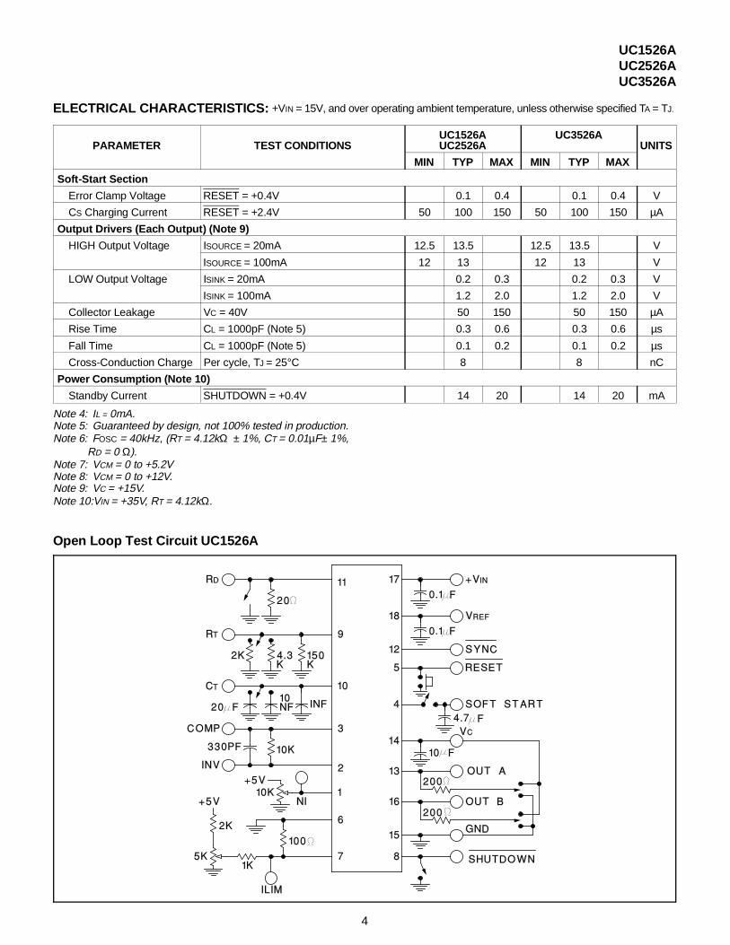
PARAMETER TEST CONDITIONSUC1526AUC2526A
UC3526AUNITS
MIN TYP MAX MIN TYP MAX
Soft-Start Section
Error Clamp Voltage RESET = +0.4V 0.1 0.4 0.1 0.4 V
CS Charging Current RESET = +2.4V 50 100 150 50 100 150 µA
Output Drivers (Each Output) (Note 9)
HIGH Output Voltage ISOURCE = 20mA 12.5 13.5 12.5 13.5 V
ISOURCE = 100mA 12 13 12 13 V
LOW Output Voltage ISINK = 20mA 0.2 0.3 0.2 0.3 V
ISINK = 100mA 1.2 2.0 1.2 2.0 V
Collector Leakage VC = 40V 50 150 50 150 µA
Rise Time CL = 1000pF (Note 5) 0.3 0.6 0.3 0.6 µs
Fall Time CL = 1000pF (Note 5) 0.1 0.2 0.1 0.2 µs
Cross-Conduction Charge Per cycle, TJ = 25°C 8 8 nC
Power Consumption (Note 10)
Standby Current SHUTDOWN = +0.4V 14 20 14 20 mA
Note 4: IL = 0mA.Note 5: Guaranteed by design, not 100% tested in production.Note 6: FOSC = 40kHz, (RT = 4.12kΩ ± 1%, CT = 0.01µF± 1%,
RD = 0 Ω).Note 7: VCM = 0 to +5.2VNote 8: VCM = 0 to +12V.Note 9: VC = +15V.Note 10:VIN = +35V, RT = 4.12kΩ.
Open Loop Test Circuit UC1526A
+VIN = 15V, and over operating ambient temperature, unless otherwise specified TA = TJ.
UC1526AUC2526AUC3526A
4
APPLICATIONS INFORMATION
Voltage ReferenceThe reference regulator of the UC1526A is based on aprecision band-gap reference, internally trimmed to ±1%accuracy. The circuitry is fully active at supply voltagesabove +7V, and provides up to 20mA of load current toexternal circuitry at +5.0V. In systems where additionalcurrent is required, an external PNP transistor can beused to boost the available current. A rugged low fre-quency audio-type transistor should be used, and leadlengths between the PWM and transistor should be asshort as possible to minimize the risk of oscillations.Even so, some types of transistors may require collec-tor-base capacitance for stability. Up to 1 amp of loadcurrent can be obtained with excellent regulation if thedevice selected maintains high current gain.
Soft-Start Circuit
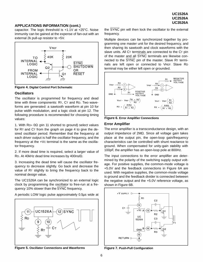
The soft-start circuit protects the power transistors andrectifier diodes from high current surges during powersupply turn-on. When supply voltage is first applied tothe UC1526A, the under-voltage lockout circuit holdsRESET LOW with Q3. Q1 is turned on, which holds thesoft-start capacitor voltage at zero. The second collectorof Q1 clamps the output of the error amplifier to ground,guaranteeing zero duty cycle at the driver outputs.When the supply voltage reaches normal operatingrange, RESET will go HIGH. Q1 turns off, allowing theinternal 100µA current source to charge CS. Q2 clampsthe error amplifier output to 1VBE above the voltage onCS. As the soft-start voltage ramps up to +5V, the dutycycle of the PWM linearly increases to whatever valuethe voltage regulation loop requires for an error null.
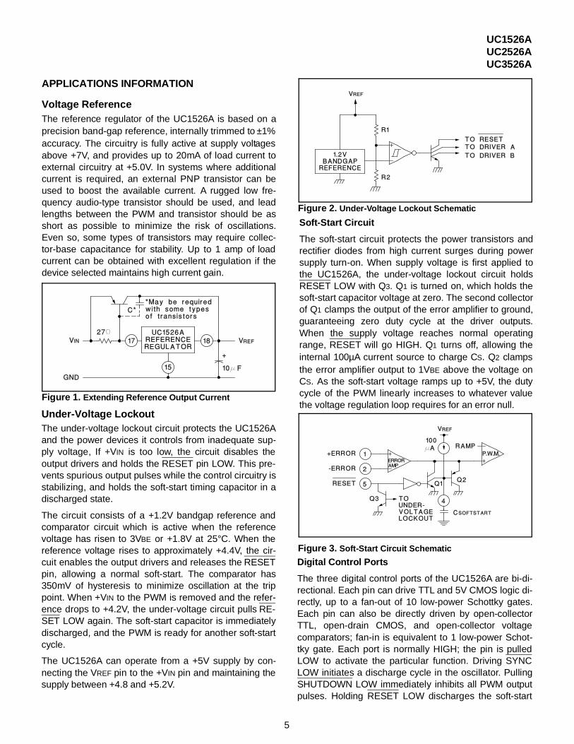
Under-Voltage LockoutThe under-voltage lockout circuit protects the UC1526Aand the power devices it controls from inadequate sup-ply voltage, If +VIN is too low, the circuit disables theoutput drivers and holds the RESET pin LOW. This pre-vents spurious output pulses while the control circuitry isstabilizing, and holds the soft-start timing capacitor in adischarged state.
The circuit consists of a +1.2V bandgap reference andcomparator circuit which is active when the referencevoltage has risen to 3VBE or +1.8V at 25°C. When thereference voltage rises to approximately +4.4V, the cir-cuit enables the output drivers and releases the RESETpin, allowing a normal soft-start. The comparator has350mV of hysteresis to minimize oscillation at the trippoint. When +VIN to the PWM is removed and the refer-ence drops to +4.2V, the under-voltage circuit pulls RE-SET LOW again. The soft-start capacitor is immediatelydischarged, and the PWM is ready for another soft-startcycle.
The UC1526A can operate from a +5V supply by con-necting the VREF pin to the +VIN pin and maintaining thesupply between +4.8 and +5.2V.
Digital Control Ports
The three digital control ports of the UC1526A are bi-di-rectional. Each pin can drive TTL and 5V CMOS logic di-rectly, up to a fan-out of 10 low-power Schottky gates.Each pin can also be directly driven by open-collectorTTL, open-drain CMOS, and open-collector voltagecomparators; fan-in is equivalent to 1 low-power Schot-tky gate. Each port is normally HIGH; the pin is pulledLOW to activate the particular function. Driving SYNCLOW initiates a discharge cycle in the oscillator. PullingSHUTDOWN LOW immediately inhibits all PWM outputpulses. Holding RESET LOW discharges the soft-start
Figure 1. Extending Reference Output Current
Figure 2. Under-Voltage Lockout Schematic
Figure 3. Soft-Start Circuit Schematic
UC1526AUC2526AUC3526A
5
capacitor. The logic threshold is +1.1V at +25°C. Noiseimmunity can be gained at the expense of fan-out with anexternal 2k pull-up resistor to +5V.
OscillatorsThe oscillator is programmed for frequency and deadtime with three components: RT, CT and RD. Two wave-forms are generated: a sawtooth waveform at pin 10 forpulse width modulation, and a logic clock at pin 12. Thefollowing procedure is recommended for choosing timingvalues:
1. With RD= 0Ω (pin 11 shorted to ground) select valuesfor RT and CT from the graph on page 4 to give the de-sired oscillator period. Remember that the frequency ateach driver output is half the oscillator frequency, and thefrequency at the +VC terminal is the same as the oscilla-tor frequency.
2. If more dead time is required, select a larger value ofRD. At 40kHz dead time increases by 400ns/Ω.
3. Increasing the dead time will cause the oscillator fre-quency to decrease slightly. Go back and decrease thevalue of RT slightly to bring the frequency back to thenominal design value.
The UC1526A can be synchronized to an external logicclock by programming the oscillator to free-run at a fre-quency 10% slower than the SYNC frequency.
A periodic LOW logic pulse approximately 0.5µs wide at
Error AmplifierThe error amplifier is a transconductance design, with anoutput impedance of 2MΩ. Since all voltage gain takesplace at the output pin, the open-loop gain/frequencycharacteristics can be controlled with shunt reactance toground. When compensated for unity-gain stability with100pF, the amplifier has an open-loop pole at 800Hz.
The input connections to the error amplifier are deter-mined by the polarity of the switching supply output volt-age. For positive supplies, the common-mode voltage is+5.0V and the feedback connections in Figure 6A areused. With negative supplies, the common-mode voltageis ground and the feedback divider is connected betweenthe negative output and the +5.0V reference voltage, asshown in Figure 6B.
the SYNC pin will then lock the oscillator to the externalfrequency.
Multiple devices can be synchronized together by pro-gramming one master unit for the desired frequency, andthen sharing its sawtooth and clock waveforms with theslave units. All CT terminals are connected to the CT pinof the master and all SYNC terminals are likewise con-nected to the SYNC pin of the master. Slave RT termi-nals are left open or connected to VREF. Slave RD
terminal may be either left open or grounded.
Figure 4. Digital Control Port Schematic
Figure 5. Oscillator Connections and Waveforms Figure 7. Push-Pull Configuration
Figure 6. Error Amplifier Connections
APPLICATIONS INFORMATION (cont.)
UC1526AUC2526AUC3526A
6

TYPICAL CHARACTERISTICS
OSCILLATOR PERIOD vs R T and CT OUTPUT BLANKING
Figure 8. Single-Ended Configuration Figure 9. Driving N-Channel Power MOSFETs
Output Drivers
The totem pole output drivers of the UC1526A are de-signed to source and sink 100mA continuously and200mA peak. Loads can be driven either from the outputpins 13 and 16, or from the +VC, as required.
Since the bottom transistor of the totem-pole is allowed tosaturate, there is a momentary conduction path from the
+VC terminal to ground during switching; however, im-proved design has limited this cross-conduction period toless than 50ns. Capacitor decoupling at VC is recom-mended and careful grounding of Pin 15 is needed to in-sure that high peak sink currents from a capacitive loaddo not cause ground transients.
APPLICATIONS INFORMATION (cont.)
UC1526AUC2526AUC3526A
7
UNITRODE INTEGRATED CIRCUITS 7 CONTINENTAL BLVD. • MERRIMACK, NH 03054TEL. (603) 424-2410 • FAX (603) 424-3460
TYPICAL CHARACTERISTICS (Cont.)
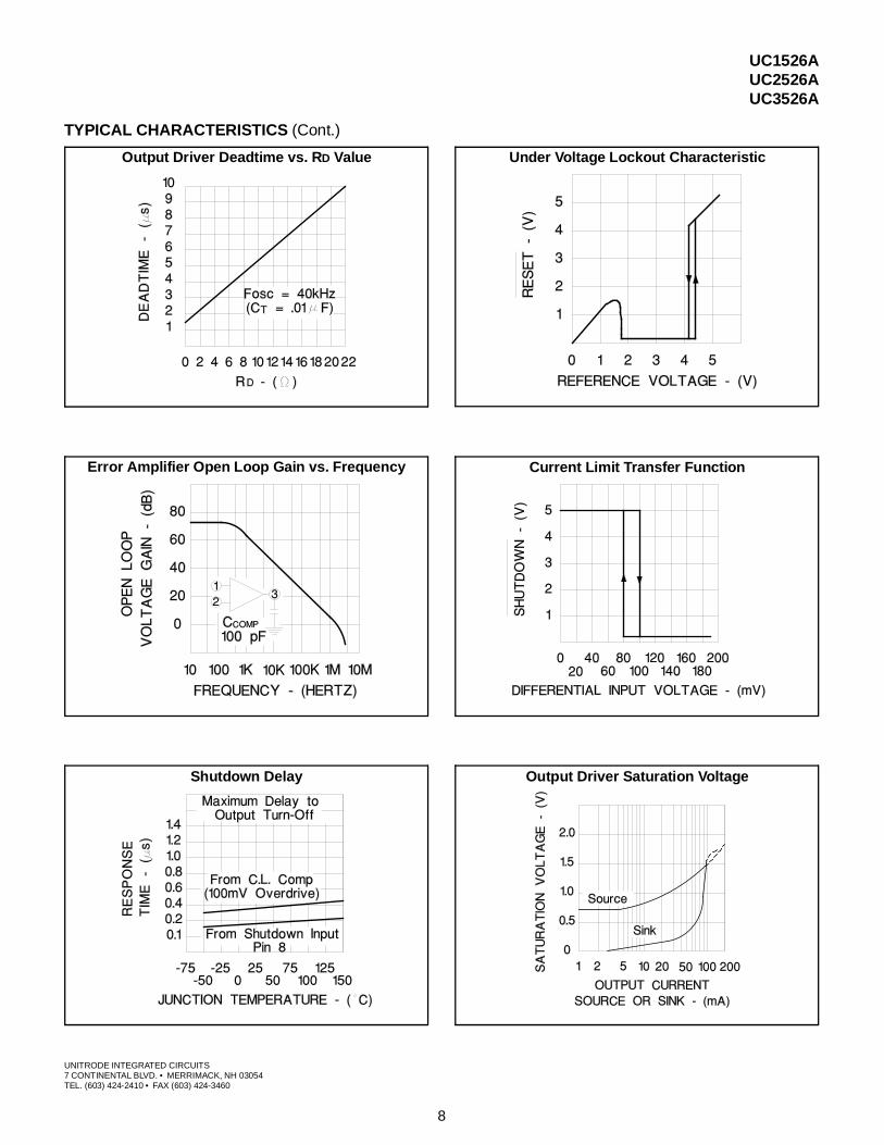
Output Driver Deadtime vs. R D Value Under Voltage Lockout Characteristic
Current Limit Transfer FunctionError Amplifier Open Loop Gain vs. Frequency
Shutdown Delay Output Driver Saturation Voltage
UC1526AUC2526AUC3526A
8
PACKAGE OPTION ADDENDUM
www.ti.com 27-Jul-2018
Addendum-Page 1
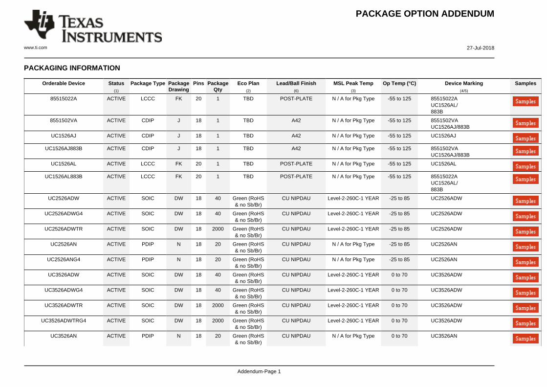
PACKAGING INFORMATION
Orderable Device Status(1)
Package Type PackageDrawing
Pins PackageQty
Eco Plan(2)
Lead/Ball Finish(6)
MSL Peak Temp(3)
Op Temp (°C) Device Marking(4/5)
Samples
85515022A ACTIVE LCCC FK 20 1 TBD POST-PLATE N / A for Pkg Type -55 to 125 85515022AUC1526AL/883B
8551502VA ACTIVE CDIP J 18 1 TBD A42 N / A for Pkg Type -55 to 125 8551502VAUC1526AJ/883B
UC1526AJ ACTIVE CDIP J 18 1 TBD A42 N / A for Pkg Type -55 to 125 UC1526AJ
UC1526AJ883B ACTIVE CDIP J 18 1 TBD A42 N / A for Pkg Type -55 to 125 8551502VAUC1526AJ/883B
UC1526AL ACTIVE LCCC FK 20 1 TBD POST-PLATE N / A for Pkg Type -55 to 125 UC1526AL
UC1526AL883B ACTIVE LCCC FK 20 1 TBD POST-PLATE N / A for Pkg Type -55 to 125 85515022AUC1526AL/883B
UC2526ADW ACTIVE SOIC DW 18 40 Green (RoHS& no Sb/Br)
CU NIPDAU Level-2-260C-1 YEAR -25 to 85 UC2526ADW
UC2526ADWG4 ACTIVE SOIC DW 18 40 Green (RoHS& no Sb/Br)
CU NIPDAU Level-2-260C-1 YEAR -25 to 85 UC2526ADW
UC2526ADWTR ACTIVE SOIC DW 18 2000 Green (RoHS& no Sb/Br)
CU NIPDAU Level-2-260C-1 YEAR -25 to 85 UC2526ADW
UC2526AN ACTIVE PDIP N 18 20 Green (RoHS& no Sb/Br)
CU NIPDAU N / A for Pkg Type -25 to 85 UC2526AN
UC2526ANG4 ACTIVE PDIP N 18 20 Green (RoHS& no Sb/Br)
CU NIPDAU N / A for Pkg Type -25 to 85 UC2526AN
UC3526ADW ACTIVE SOIC DW 18 40 Green (RoHS& no Sb/Br)
CU NIPDAU Level-2-260C-1 YEAR 0 to 70 UC3526ADW
UC3526ADWG4 ACTIVE SOIC DW 18 40 Green (RoHS& no Sb/Br)
CU NIPDAU Level-2-260C-1 YEAR 0 to 70 UC3526ADW
UC3526ADWTR ACTIVE SOIC DW 18 2000 Green (RoHS& no Sb/Br)
CU NIPDAU Level-2-260C-1 YEAR 0 to 70 UC3526ADW
UC3526ADWTRG4 ACTIVE SOIC DW 18 2000 Green (RoHS& no Sb/Br)
CU NIPDAU Level-2-260C-1 YEAR 0 to 70 UC3526ADW
UC3526AN ACTIVE PDIP N 18 20 Green (RoHS& no Sb/Br)
CU NIPDAU N / A for Pkg Type 0 to 70 UC3526AN
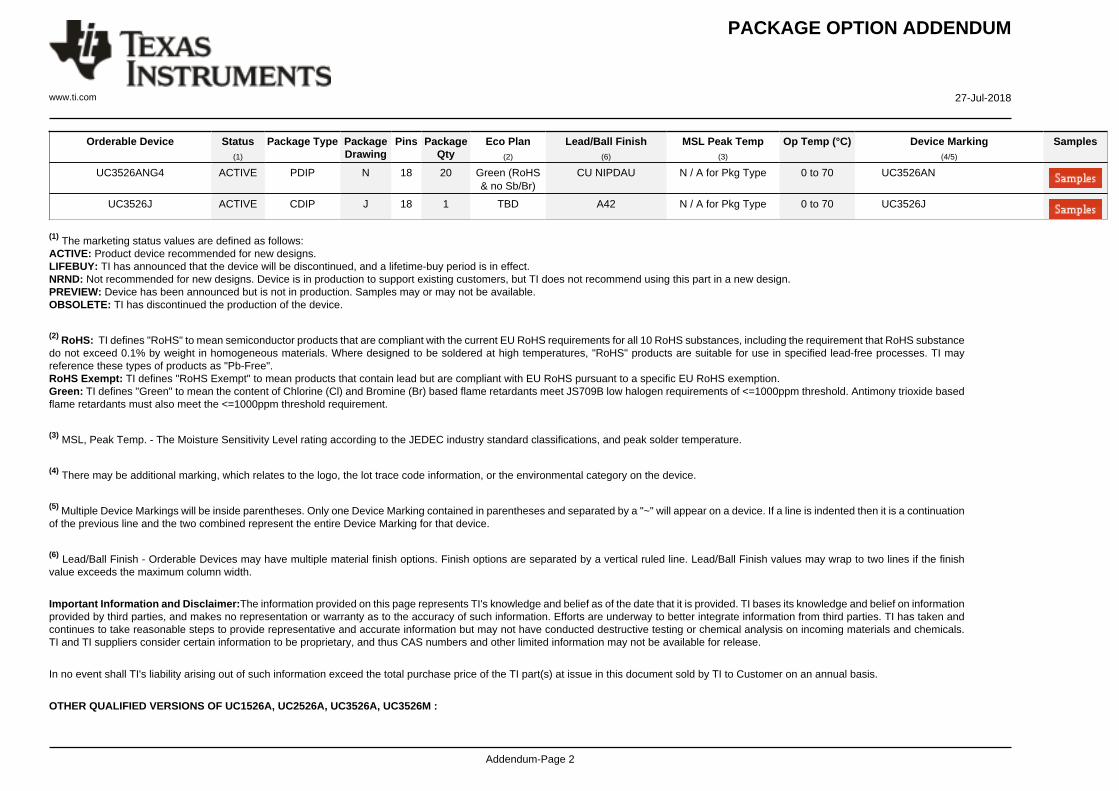
PACKAGE OPTION ADDENDUM
www.ti.com 27-Jul-2018
Addendum-Page 2
Orderable Device Status(1)
Package Type PackageDrawing
Pins PackageQty
Eco Plan(2)
Lead/Ball Finish(6)
MSL Peak Temp(3)
Op Temp (°C) Device Marking(4/5)
Samples
UC3526ANG4 ACTIVE PDIP N 18 20 Green (RoHS& no Sb/Br)
CU NIPDAU N / A for Pkg Type 0 to 70 UC3526AN
UC3526J ACTIVE CDIP J 18 1 TBD A42 N / A for Pkg Type 0 to 70 UC3526J
(1) The marketing status values are defined as follows:ACTIVE: Product device recommended for new designs.LIFEBUY: TI has announced that the device will be discontinued, and a lifetime-buy period is in effect.NRND: Not recommended for new designs. Device is in production to support existing customers, but TI does not recommend using this part in a new design.PREVIEW: Device has been announced but is not in production. Samples may or may not be available.OBSOLETE: TI has discontinued the production of the device.
(2) RoHS: TI defines "RoHS" to mean semiconductor products that are compliant with the current EU RoHS requirements for all 10 RoHS substances, including the requirement that RoHS substancedo not exceed 0.1% by weight in homogeneous materials. Where designed to be soldered at high temperatures, "RoHS" products are suitable for use in specified lead-free processes. TI mayreference these types of products as "Pb-Free".RoHS Exempt: TI defines "RoHS Exempt" to mean products that contain lead but are compliant with EU RoHS pursuant to a specific EU RoHS exemption.Green: TI defines "Green" to mean the content of Chlorine (Cl) and Bromine (Br) based flame retardants meet JS709B low halogen requirements of <=1000ppm threshold. Antimony trioxide basedflame retardants must also meet the <=1000ppm threshold requirement.
(3) MSL, Peak Temp. - The Moisture Sensitivity Level rating according to the JEDEC industry standard classifications, and peak solder temperature.
(4) There may be additional marking, which relates to the logo, the lot trace code information, or the environmental category on the device.
(5) Multiple Device Markings will be inside parentheses. Only one Device Marking contained in parentheses and separated by a "~" will appear on a device. If a line is indented then it is a continuationof the previous line and the two combined represent the entire Device Marking for that device.
(6) Lead/Ball Finish - Orderable Devices may have multiple material finish options. Finish options are separated by a vertical ruled line. Lead/Ball Finish values may wrap to two lines if the finishvalue exceeds the maximum column width.
Important Information and Disclaimer:The information provided on this page represents TI's knowledge and belief as of the date that it is provided. TI bases its knowledge and belief on informationprovided by third parties, and makes no representation or warranty as to the accuracy of such information. Efforts are underway to better integrate information from third parties. TI has taken andcontinues to take reasonable steps to provide representative and accurate information but may not have conducted destructive testing or chemical analysis on incoming materials and chemicals.TI and TI suppliers consider certain information to be proprietary, and thus CAS numbers and other limited information may not be available for release.
In no event shall TI's liability arising out of such information exceed the total purchase price of the TI part(s) at issue in this document sold by TI to Customer on an annual basis.
OTHER QUALIFIED VERSIONS OF UC1526A, UC2526A, UC3526A, UC3526M :
PACKAGE OPTION ADDENDUM
www.ti.com 27-Jul-2018
Addendum-Page 3
• Catalog: UC3526A, UC3526AM, UC3526
• Military: UC2526AM, UC1526A, UC1526
NOTE: Qualified Version Definitions:
• Catalog - TI's standard catalog product
• Military - QML certified for Military and Defense Applications
IMPORTANT NOTICE
Texas Instruments Incorporated (TI) reserves the right to make corrections, enhancements, improvements and other changes to itssemiconductor products and services per JESD46, latest issue, and to discontinue any product or service per JESD48, latest issue. Buyersshould obtain the latest relevant information before placing orders and should verify that such information is current and complete.TI’s published terms of sale for semiconductor products (http://www.ti.com/sc/docs/stdterms.htm) apply to the sale of packaged integratedcircuit products that TI has qualified and released to market. Additional terms may apply to the use or sale of other types of TI products andservices.Reproduction of significant portions of TI information in TI data sheets is permissible only if reproduction is without alteration and isaccompanied by all associated warranties, conditions, limitations, and notices. TI is not responsible or liable for such reproduceddocumentation. Information of third parties may be subject to additional restrictions. Resale of TI products or services with statementsdifferent from or beyond the parameters stated by TI for that product or service voids all express and any implied warranties for theassociated TI product or service and is an unfair and deceptive business practice. TI is not responsible or liable for any such statements.Buyers and others who are developing systems that incorporate TI products (collectively, “Designers”) understand and agree that Designersremain responsible for using their independent analysis, evaluation and judgment in designing their applications and that Designers havefull and exclusive responsibility to assure the safety of Designers' applications and compliance of their applications (and of all TI productsused in or for Designers’ applications) with all applicable regulations, laws and other applicable requirements. Designer represents that, withrespect to their applications, Designer has all the necessary expertise to create and implement safeguards that (1) anticipate dangerousconsequences of failures, (2) monitor failures and their consequences, and (3) lessen the likelihood of failures that might cause harm andtake appropriate actions. Designer agrees that prior to using or distributing any applications that include TI products, Designer willthoroughly test such applications and the functionality of such TI products as used in such applications.TI’s provision of technical, application or other design advice, quality characterization, reliability data or other services or information,including, but not limited to, reference designs and materials relating to evaluation modules, (collectively, “TI Resources”) are intended toassist designers who are developing applications that incorporate TI products; by downloading, accessing or using TI Resources in anyway, Designer (individually or, if Designer is acting on behalf of a company, Designer’s company) agrees to use any particular TI Resourcesolely for this purpose and subject to the terms of this Notice.TI’s provision of TI Resources does not expand or otherwise alter TI’s applicable published warranties or warranty disclaimers for TIproducts, and no additional obligations or liabilities arise from TI providing such TI Resources. TI reserves the right to make corrections,enhancements, improvements and other changes to its TI Resources. TI has not conducted any testing other than that specificallydescribed in the published documentation for a particular TI Resource.Designer is authorized to use, copy and modify any individual TI Resource only in connection with the development of applications thatinclude the TI product(s) identified in such TI Resource. NO OTHER LICENSE, EXPRESS OR IMPLIED, BY ESTOPPEL OR OTHERWISETO ANY OTHER TI INTELLECTUAL PROPERTY RIGHT, AND NO LICENSE TO ANY TECHNOLOGY OR INTELLECTUAL PROPERTYRIGHT OF TI OR ANY THIRD PARTY IS GRANTED HEREIN, including but not limited to any patent right, copyright, mask work right, orother intellectual property right relating to any combination, machine, or process in which TI products or services are used. Informationregarding or referencing third-party products or services does not constitute a license to use such products or services, or a warranty orendorsement thereof. Use of TI Resources may require a license from a third party under the patents or other intellectual property of thethird party, or a license from TI under the patents or other intellectual property of TI.TI RESOURCES ARE PROVIDED “AS IS” AND WITH ALL FAULTS. TI DISCLAIMS ALL OTHER WARRANTIES ORREPRESENTATIONS, EXPRESS OR IMPLIED, REGARDING RESOURCES OR USE THEREOF, INCLUDING BUT NOT LIMITED TOACCURACY OR COMPLETENESS, TITLE, ANY EPIDEMIC FAILURE WARRANTY AND ANY IMPLIED WARRANTIES OFMERCHANTABILITY, FITNESS FOR A PARTICULAR PURPOSE, AND NON-INFRINGEMENT OF ANY THIRD PARTY INTELLECTUALPROPERTY RIGHTS. TI SHALL NOT BE LIABLE FOR AND SHALL NOT DEFEND OR INDEMNIFY DESIGNER AGAINST ANY CLAIM,INCLUDING BUT NOT LIMITED TO ANY INFRINGEMENT CLAIM THAT RELATES TO OR IS BASED ON ANY COMBINATION OFPRODUCTS EVEN IF DESCRIBED IN TI RESOURCES OR OTHERWISE. IN NO EVENT SHALL TI BE LIABLE FOR ANY ACTUAL,DIRECT, SPECIAL, COLLATERAL, INDIRECT, PUNITIVE, INCIDENTAL, CONSEQUENTIAL OR EXEMPLARY DAMAGES INCONNECTION WITH OR ARISING OUT OF TI RESOURCES OR USE THEREOF, AND REGARDLESS OF WHETHER TI HAS BEENADVISED OF THE POSSIBILITY OF SUCH DAMAGES.Unless TI has explicitly designated an individual product as meeting the requirements of a particular industry standard (e.g., ISO/TS 16949and ISO 26262), TI is not responsible for any failure to meet such industry standard requirements.Where TI specifically promotes products as facilitating functional safety or as compliant with industry functional safety standards, suchproducts are intended to help enable customers to design and create their own applications that meet applicable functional safety standardsand requirements. Using products in an application does not by itself establish any safety features in the application. Designers mustensure compliance with safety-related requirements and standards applicable to their applications. Designer may not use any TI products inlife-critical medical equipment unless authorized officers of the parties have executed a special contract specifically governing such use.Life-critical medical equipment is medical equipment where failure of such equipment would cause serious bodily injury or death (e.g., lifesupport, pacemakers, defibrillators, heart pumps, neurostimulators, and implantables). Such equipment includes, without limitation, allmedical devices identified by the U.S. Food and Drug Administration as Class III devices and equivalent classifications outside the U.S.TI may expressly designate certain products as completing a particular qualification (e.g., Q100, Military Grade, or Enhanced Product).Designers agree that it has the necessary expertise to select the product with the appropriate qualification designation for their applicationsand that proper product selection is at Designers’ own risk. Designers are solely responsible for compliance with all legal and regulatoryrequirements in connection with such selection.Designer will fully indemnify TI and its representatives against any damages, costs, losses, and/or liabilities arising out of Designer’s non-compliance with the terms and provisions of this Notice.
Mailing Address: Texas Instruments, Post Office Box 655303, Dallas, Texas 75265Copyright © 2018, Texas Instruments Incorporated