5. puwma pulse width modulator
TRANSCRIPT

5. PUWMA PULSE WIDTH MODULATOR The PUWMA pulse width modulator is the latest addition to the FAT5 range of modules. It is a more complex modulator than the analogue designs, but the high efficiency of pulse width modulation gives a considerable reduction in heat generation and power consumption making this method of modulation tempting for higher power transmitters, for battery powered builds, or compact designs where heat dissipation can be a problem.
Fig 5.1 PUWMA size illustration Fig 5.2 assembled PCB What is Pulse width Modulation? PWM as the name suggests is a circuit that varies the width of a square wave pulse. There are several methods of achieving pulse width modulation. PUWMA uses a comparator circuit to compare the input signal with a 150 kHz sawtooth waveform. The output from the comparator is a 150kHz square wave of variable symmetry, depending on whether the input signal is larger or smaller than the sawtooth waveform at any instant. See figure 5.3 below. The percentage of time the square wave is at maximum volts is called the duty cycle. The duty cycle varies with the amplitude of the audio applied to the circuit. With no audio input, or as the amplitude momentarily crosses zero volts (level 2 in figure 5.3), the duty cycle is 50%. This level would be the resting carrier position.
Figure 5.3 Generating a square wave by comparing audio to a sawtooth waveform
As the audio input becomes more positive (level 3 in figure 3) the duty cycle increases towards 100% (where there is effectively no pulse at all, just a maximum output voltage at that moment) . When the audio input goes negative (level 1 in figure 3) the duty cycle reduces from 50% to a point where it is 0% (where there is effectively no pulse at all, just a minimum output voltage at that moment). In a perfect system an audio signal applied to the PWM will produce a square wave output pulse of constant amplitude and constant frequency, but with the duty cycle varying between 0% and 100%, with 50% being the resting carrier point. The audio input signal has modulated the 150 kHz frequency square wave by means of varying its duty cycle. The sampling rate of 150 kHz is chosen to be many times greater than the highest audio input frequency. The reasons for this will be explained later. Why use PWM? Why the complexity? Why not just use a more conventional series modulator? A simple answer, efficiency. An analogue series modulator dissipates at least as much power in heat as the RF PA consumes in total because it forms the top half of a potential divider, with the RF PA forming the bottom half.. e.g. A 100W RF PA that is 80% efficient is consuming 125W, so the modulator must also dissipate 125W to keep the PA voltage at half HT (allowing the modulation to vary the HT from zero to maximum). So, 125W of heat for 100W RF. A pulse width modulator achieves the same thing as a conventional series modulator but with much less dissipation. Efficiency is 95% or greater. So, in the above example a pulse width modulator supplying 125W of power to the RF PA at 95% efficiency is using 131.5W, losing only 6.5W as heat as opposed to 125W. Why is PWM so efficient? PWM is a digital system. That is, the output is either zero (0) or maximum (1). This switching action is done by a pair of MOSFETS which can change state very quickly. When they are off they consume no power. When they are fully on they present a resistance of only 0.18 ohms each. Power is wasted as heat during the 0-1 or 1-0 transition but this is only a very small percentage of the total time. In a standard series modulator, the series transistors are behaving like variable resistors all the time and are thus constantly dissipating energy.

Circuit Basics Figure 5.4 below is a much simplified PUWMA circuit showing the sawtooth generator and comparator mentioned earlier. The logic-level PWM output signal from the comparator is referenced to earth, but we need to control a transistor connected to HT with the load connected to the emitter. This is called high-side drive. There are many ways of managing the level conversion, but one of the easiest methods in digital systems is to use an opto-isolator. The PWM waveform is thus transferred to the switching transistor (shown here inside the opto isolator module) where it is now a low impedance signal that can supply real power to the RF PA. It is the fact this transistor is always fully on or fully off that makes the circuit so efficient.
Fig 5.4 Simplified diagram of PWM system
Filtering There is just one more thing that needs to be addressed before we connect the PWM signal to the PA. Applying a 150kHz square wave as a modulating signal to an RF PA will produce sidebands every 150kHz up and down the band and not a lot in the way of recognisable audio. So first we pass the signal through a low pass filter (LPF) to recover the audio energy from the waveform and attenuate the 150kHz (and odd harmonics) signal. The filter used with PUWMA is a 4-pole filter with a roll-off starting just outside the audio passband. At 150 kHz the attenuation is very high (-80dB). What appears out of the filter is an average DC level based on the width of the PWM pulses. This is one reason we use a high switching frequency - it is easy to filter out a frequency that is so much higher than the audio we need to recover. Aliasing There is another more technical reason for the high sampling frequency, to do with a fact of life in sampled systems called aliasing. The sawtooth audio sampling frequency needs to be at least twice the highest frequency we expect to sample otherwise the output is not a correct representation of the input. This frequency is called the Nyquist frequency, named after Harry Nyquist of sampling theory fame. So with 150 kHz sampling we'd only hit problems if the audio reached 75 kHz. Theoretically, any input frequency above 75kHz would appear as an alias of itself in the output. For instance a 76kHz signal would also appear as 74kHz. If the sampling rate was so low that aliasing could occur an anti-aliasing filter could be applied to the input signal to restrict bandwidth to below the Nyquist frequency. This is not needed here although the bandwidth of the audio should nonetheless be tightly controlled to produce tightly controlled sidebands in the modulated RF envelope. The FAT-MAX audio processor (described in section 1 of this document) uses an 8 pole switched capacitor filter to control bandwidth and is very effective. Before going on to describe the actual PUWMA circuit in detail, let's first return to the circuitry around the opto-isolator shown in figure 5.4 above. In practice a little more circuitry is needed to change the opto-isolator output into a suitable signal for high-side driving a power MOSFET. This is where another concept comes in: the floating earth.

Floating Earth The floating earth concept can be confusing at first, and as it is a core part of the PUWMA circuit it's worth spending a little time on an explanation using a simple illustration. Consider Figure 5.5 (A) below. This shows a 9V transistor radio powered from a 9V battery, where the 0V side is connected to earth. Now look at 5.5(B). Here we have the same radio powered by the same battery, but this time we have added another battery in series. The radio's 0V line is now at 9V with respect to real earth, but as far as the radio is concerned, nothing has changed. The radio's 0V is now a floating earth. Figure 5.5(C) takes the same concept and applies it to a representation of what is happening in PUWMA. Instead of the radio we now have a FET driver, with its own LT supply. The FET driver rapidly switches the FET on and off, rather like a simple toggle switch. When the switch is open, LT- is at earth potential (HT-) because there is no voltage drop across the load as no current flows. When the switch is closed, HT+ is applied to the load, raising the level of the floating earth LT- and also LT+. The FET driver knows nothing of this because the LT voltage i.e. the potential difference between LT- and LT+ doesn't change. (The output pulse width is determined by the time during which the switch is closed, and the frequency by the number of open/close operations per second).
Figure 5.5. The floating earth concept
Taking this a little further by adding in some more detail, figure 5.6 below is pretty close to the actual PUWMA circuitry, and the component numberings are the same.
. Figure 5.6 simplified floating earth drive system
U4 is powered from a floating supply, but the HT supply that actually supplies the PWM output signal is referenced to real earth. When U4 output goes high, Q3 and Q4 are turned on, effectively performing a switching action and connecting the full HT to the output, in this case the LPF. (D5 is a clamp diode to prevent the output going negative and damp any ringing from the LPF). Hopefully the actual PUWMA circuit diagram (figure 5.8 below) should now be a little clearer.
Circuit Description
U1 is an SMPSU PWM chip that is well suited for use as a pulse width modulator as it has a fast response allowing it to work at audio frequencies. It is a complex chip, but for our purposes it is little more than a sawtooth generator and comparator as shown in figure 5.4. The sawtooth frequency is nominally 150 kHz. Line level audio (e.g. from the FAT-MAX processor) is applied via RV2, then through C3 where it is combined with a DC level from RV1. With no audio input, the DC level alone determines the mark/space ratio of the output pulse, and hence, after smoothing in the LPF, the output voltage (which controls the carrier level in the RF section). RV1 is set to produce a 40% duty cycle pulse under no-mod conditions. This will be covered later as part of the set-up description. The components around U1 are in accordance with the data sheet recommendations for the IC. A down-side of the IC is the need to provide a working voltage above 13V in order to disable the low-voltage close-down circuitry it contains. Above 14V the IC draws substantially more current but within the 13V to 14V range things work reliably, and a typical 13.8V supply will work fine. The PWM pulses appearing at U1 pin 4 are fed to the opto-isolator U2, with the output side (U2 pin 6 ) referenced to the floating earth. Floating Power supply To avoid the need for a separate external floating supply, this is produced locally. The current requirements are very modest (about 35mA). U1 is running all the time, and the pulses at pin 4, as well as being fed to U1, are also fed to U3 which is an identical FET driver to U4. (U3 can actually be an inverting or non-inverting type, but usually the inverting type will be supplied to keep U3 and U4 the same) . The output from U4 passes through C9 and T1 after which it is full-wave rectified by diodes D1-D4. Full wave rectification makes use of both peaks and troughs of the PWM pulse regardless of the duty cycle. The transformer isolates the secondary so that the level can float. The regulated floating supply is permanently present ensuring a clean start-up on each transmit period. Primary side components are shown within the dotted box. The output from D1-D4 is regulated by VR1 to provide 8V to power U4 (8V gives a better FET drive level than 5V). The floating 8V line is further regulated down to 5V by VR2 to power the secondary side of U2. PWM switching The open collector output of U2 pin 6 is connected to 5V via R1, which also supplies 5V to the input of the FET driver U4, unless pin 6 of U2 is pulled low by the PWM drive. With no drive U4 pin 2 is at 5V, and being an inverting driver, the output at pins 6 and 7 are at floating earth potential, thus Q3 and Q4 are not cut-on and no power is supplied to the RF PA. This is a fail-safe circuit ensuring RF stops if the PWM drive fails. With drive present, the power switching FETs Q3 and Q4 apply a pulsed version of the main HT to the output at TB2/3 after which the pulses are passed through the low pass filter (LPF) to remove the 150kHz sampling signal and recover the DC component. Low Pass Filter The filter components are contained on a separate PCB or chassis mounted. Because the filter is vital to ensuring a spectrally pure signal we have decided to only supply components

with the LPF parts included. The LPF PCB need not be purchased if direct chassis mounting is planned. See the purchasing options on the kits page at s9plus.com. L1,L2 and C18-C23 form a 4-pole low pass filter with a -3dB point around 15kHz and an attenuation at 150 kHz of some 80dB. This level of attenuation is more than sufficient to ensure no unwanted sidebands appear on the carrier every 150 kHz.
Figure 5.7 LPF board (prototype shown, not actual PCB)
PTT A way is needed to control the transmitter keying. Removing PWM drive removes HT from the RF PA as described earlier, and a rather crude but effective method is used to achieve this. Drive from U1 feeds U2 via R11, a limiting resistor for the LED inside U2. When Q1 is cut on, R11 is shorted to earth and the drive is removed. Q1 is cut on because its base is biased on via R16 and R10. This is the standby condition. Earthing TB1/5 removes the Q1 base bias, Q1 is cut off, and drive is applied to U2. A second PTT option is provided for interfacing to systems where it is more convenient to apply a voltage to transmit rather than an earth. Q2 collector sits across Q1 base but with no voltage applied to TB1/7 it is inactive. Applying nominally 5V to TB1/7 cuts Q2 on thus removing bias from Q1 base and applying drive.

Figure 5.8 PUWMA circuit diagram
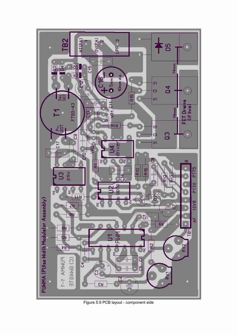
Figure 5.9 PCB layout - component side

Figure 5.10 LPF PCB layout.

PUWMA PARTS LIST MAIN PCB
Component Value / Description
R1 1k All ¼ W carbon film, 5% or better
R2 18k
R3 10k
R4 2k2
R5 2k2
R6 2k2
R7 18k
R8 56k
R9 1k
R10 4k7
R11 1k
R12 2k2
R13 4k7
R14 47R
R15 47R
R16 4k7
RV1 5K lin. 5mm pitch
RV2 5k lin. 5mm pitch
C1 0.1uF, 100n, 104 polyester
C2 47uF electrolytic, >16VW
C3 47uF electrolytic, >16VW
C4 1n, 102 polyester
C5 220pF ceramic
C6 0.47uF, 470n, 474
C7 47uF electrolytic, >16VW
C8 1000pF, 102 polyester
C9 0.47uF, 470n, 474
C10 0.1uF, 100n, 104 polyester
C11 0.1uF, 100n, 104 polyester
C12 47uF electrolytic, >16VW
C13 0.1uF, 100n, 104 polyester
C14 0.1uF, 100n, 104 polyester
C15 0.1uF, 100n, 104 >63VW
C16 100uF low ESR electrolytic, 63V 105deg
C17 0.1uF, 100n, 104 polyester
Q1, Q2 2N3904 TO-92
Q3, Q4 IRF640 + mica mounting kits / screws
D1-4 BAT85
D5 BYW80-200 + mica mounting kit / screw
U1 UCC25701 14pin DIP inc skt
U2 6N137 8pin DIP inc skt
U3, U4 TC4421 8 pin DIP inc skts

PUWMA PARTS LIST MAIN PCB Cont'd
Component Value / Description
VR1 78L08 TO-92
VR2 78L05 TO-92
T1 core FT50-43 pri. 20T sec. 30T over-wound
TB1 8 pin header strip with mating conn.
TB2 3 terminal connector block
PUWMA PARTS LIST LPF PCB
Component Value / Description
C18-23 1uF 100VW
L1 36uH 20 turns # - see photo
L2 88uH 32 turns # -see photo
# wire use live or neutral from 5A twin/earth solid mains cable
Construction Notes - main PCB Refer to the PCB layout and the component list. It will help if you print out a copy of those pages to refer to as you proceed. On the list, tick the components off as they are installed. Construction is straightforward as there are no surface mounted or otherwise tricky components to solder. Make sure you are confident that your soldering skills are up to the task. At S9-kits we have had very few returns, but they have all been due to bad soldering. We suggest you start by soldering the IC sockets in place to act as landmarks. Make sure you fit them the right way round. Just solder a couple of diagonal pins to hold the socket in place then re-check orientation and alignment before soldering the remaining pins. After that it's your choice, but it makes sense to add the smallest parts first, in which case start with the resistors, then the small capacitors, then the transistors and regulators. finish off by adding the terminals and the larger capacitors. Double-check that the electrolytics are inserted the correct way round. Winding T1 T1 isolates the driver U3 from the floating supply so the wire insulation must be able to cope with several tens of volts between primary and secondary depending on the main HT being used. We have had no trouble when using normal enamelled wire, and something around 28 - 32 swg is fine. As long as the turns fit in the core it should work ok. Just wind the 30 turn secondary on the core, then over-wind with the 20 turn primary, spacing it out to cover the same amount of core as the secondary. It's not critical, and we'll check the circuit is working properly later. (There's probably a better number of turns and a better core that could be used, but this works fine. If anyone has suggestions here please let us know). Don't glue the core onto the PCB until the circuit has been checked, but when all is ok, glue the core to the PCB with superglue, glue-gun glue, or whatever is preferred. What heatsink? As a guide, the heatsink shown in figure 5.1 is way larger than needed. After running a 100W carrier for one hour the heatsink was barely warm. (No fan cooling used). As we discussed earlier, there is not much heat generated so requirements here are modest. In fact for most applications if the board is mounted in say a die-cast box, itself attached to a metal chassis, that is more than adequate.

Mounting D5,Q3,Q4 Note the mounting tabs aren't isolated from the pins. D5 tab is connected to the cathode pin. Q3 and Q4 tabs are connected to the drain pins. Mounting these parts pretty much depends on how you have chosen to dissipate heat (see above). Using a piece of right angle aluminium between the devices and the heatsink is ideal. A little metalwork and some dexterity is needed here. If the heatsink is not floating you will need to isolate the devices using the mica insulation kits supplied. You can use the black plastic collars in two ways depending on whether or not you want to isolate the fixing screws from the heatsink or from the devices. PWM output is via screw terminal TB2/3 but you could take a feed from the screw on D5 if more convenient. Figure 5.11 below shows how a piece of right angle aluminium was used as a heatsink coupler (PCB is a prototype). The heatsink coupler is also used as the main PCB mounting method.
Figure 5.11 Coupling to heatsink example
When you do attach the heatsink use a test meter to ensure there are no shorts. If more convenient you could attach the power devices to an entirely separate heatsink away from the main PCB. (We haven't tried this)
Construction Notes - LPF If you have chosen not to use the PCB, use short leads on the capacitors to minimise inductance, and position the inductors so as to minimise mutual coupling e.g. mount 'pancake' style side-by-side as on the PCB, or make sure the cores are at right angles to each other. Add the capacitors and terminal blocks first then you can see the clearance needed for the two inductors. The capacitors are non-polarised. The dust-iron cores are identical for L1 and L2. The only difference is the number of turns used. Make sure after winding that you place the 36uH inductor at the input and the 88uH inductor with more turns at the output. Wire In the UK a suitable wire is the solid live or neutral wire from 5A twin/earth mains cable. You will need approx 1m for L1 (20 turns) and 1.5m for L2 (32 turns) So, use both live and neutral from 1.5m of cable. Winding L1 and L2 Winding the cores is easier if you follow these guidelines: - practice this method with some more flexible wire first. - hold the empty core in your right hand so that you are looking down through the hole and your thumb is on the top surface of the core - thread the wire through the hole from underneath, and clamp it between your right thumb and the core, halfway along the wire.

- with your left hand bend the wire that's under the core around the outside of the core and continue bending so that it lays over the top surface of the core, across middle of the hole - now push the wire down through the hole using your left thumb until the loop of wire formed is accessible from the underside - insert your left forefinger through the loop of wire under the core and pull the wire through making sure you still keep the wire clamped with your right thumb. - repeat for each turn, then use the same method for the other half of the wire. That's all there is to it. This method makes sure there is tension in the windings. It is easier to pull the wire though than push it through. Space the wire roughly as shown in figure 5.7 Note: One turn is one pass through the hole, so what may be regarded as the first turn is actually two turns as there are two passes through the core. Attaching L1 and L2 to the PCB or chassis The cores are reasonably heavy so some means of securing should be used. PCB holes are provided for clamping the cores using a screw (not supplied) through the centre, and a circular or oblong piece of wood, plastic or perspex (or similar). Ensure that the clamping method doesn't create a shorted turn through the core.