reduction of threading dislocation density in top-down
TRANSCRIPT

Reduction of threading dislocation density in top-down fabricated GaNnanocolumns via their lateral overgrowth by MOCVD
Zubialevich, V., McLaren, M., Pampili, P., Shen, J., Arredondo-Arechavala, M., & Parbrook, P. J. (2020).Reduction of threading dislocation density in top-down fabricated GaN nanocolumns via their lateral overgrowthby MOCVD. Journal of Applied Physics, 127(2), [025306]. https://doi.org/10.1063/1.5110602
Published in:Journal of Applied Physics
Document Version:Peer reviewed version
Queen's University Belfast - Research Portal:Link to publication record in Queen's University Belfast Research Portal
Publisher rights© 2019 The Authors. This work is made available online in accordance with the publisher’s policies. Please refer to any applicable terms ofuse of the publisher.
General rightsCopyright for the publications made accessible via the Queen's University Belfast Research Portal is retained by the author(s) and / or othercopyright owners and it is a condition of accessing these publications that users recognise and abide by the legal requirements associatedwith these rights.
Take down policyThe Research Portal is Queen's institutional repository that provides access to Queen's research output. Every effort has been made toensure that content in the Research Portal does not infringe any person's rights, or applicable UK laws. If you discover content in theResearch Portal that you believe breaches copyright or violates any law, please contact [email protected].
Download date:13. Mar. 2022

1
Reduction of threading dislocation density in top-down fabricated GaN
nanocolumns via their lateral overgrowth by MOCVD
Vitaly Z. Zubialevich a, Mathew McLaren b, Pietro Pampili a, John Shen c,
Miryam Arredondo-Arechavala b, *, Peter J. Parbrook a, d, †
a Tyndall National Institute, University College Cork, Cork, T12 R5CP, Ireland.
b Centre for Nanostructured Media, School of Mathematics and Physics, Queen’s University,
Belfast, BT7 1NN, N. Ireland; * E-mail: [email protected]
c Electrical and Computer Engineering Department, Illinois Institute of Technology, Chicago,
IL 60616, Illinois, USA
d School of Engineering, University College Cork, Cork, Ireland; †E-mail: [email protected]
1 Abstract
Reduction of threading dislocation density in top-down fabricated GaN nanocolumns
(NCs) via their successive lateral shrinkage by anisotropic wet etch and lateral
overgrowth by MOCVD is studied by transmission electron microscopy (TEM). The
fabrication process involves a combination of dry and wet etches to produce NC
arrays of low fill factor (<5%) which are then annealed and laterally overgrown to
increase the array fill factor to around 20-30%. The resulting NC arrays show a
reduction in treading dislocation density of at least 25 times, allowing for the
reduction in material volume due to the array fill factor, with dislocations being
observed to bend into the voids between NCs during the overgrowth process.
2 Introduction
Gallium nitride and other wide bandgap semiconductors have received much
attention in recent years for a variety of applications in optoelectronics and high
temperature, high power devices [1-4]. Film growth on substrates such as silicon and
sapphire is the most common device preparation method [5, 6], with the aim of
producing transistors with high electron mobility. However, a key issue with the
growth of these films is the presence of threading dislocations (TDs), a concern when
fabricating GaN-based semiconductor devices due to the negative effects they may
have on device quality such as increased current leakage [7, 8], decreased efficiency
and lifetime [9], disrupted electric field distribution and a premature breakdown due
to microplasmas [10, 11]. Dislocation densities in the range of 108 cm−2 to 1010 cm−2
are often recorded for few-to-several micrometer-thick heteroepitaxially grown GaN
films [12, 13]. While light emitting diodes, which only need to operate in forward bias,
may be fabricated from material with such high TD densities (TDDs) [10, 14], for high

2
power or high temperature applications it is imperative that TDD should be
considerably reduced to produce quality devices.
One such method of TDD reduction, for example, is the annealing of nanostructured
GaN to temperatures of 900°C [15]. Nanostructuring of GaN is a proven method for
TD reduction. This can include the extra growth steps such as the creation of
interlayers of SiNx or ScN which act to stop dislocations from propagating [16, 17].
Another approach for dislocation reduction involves epitaxial lateral overgrowth [18,
19], which is a second stage of GaN growth after the initial GaN formation and
patterning (typically on the microscale). The latter has been very successful for
reducing TDDs by several orders of magnitude, closer to values of 106-107 cm−2.
Finally, nanostructured GaN in the form of nanocolumn (NC) arrays is found to be an
effective method of dislocation reduction [20]. Due to the higher surface-to-volume
area it is potentially easier to achieve dislocation reduction in nanostructured
materials. Notably, when prepared by a bottom-up approach, GaN NCs with a small
enough diameter are observed to be dislocation free due to dislocation bending
towards NC sidewalls at early stages of growth [21]. In general this method is less
suitable for mass-production of potential devices due to (a) unavoidable variability in
individual NCs dimensions, particularly, height, (b) apex tops of grown NCs (when
grown Ga-polar), (c) limited achievable fill factor of their arrays, and finally (d) issues
with controlling doping levels. In contrast, many of these issues may be avoided by
fabricating NC arrays using ”top-down” fabrication approaches [22].
Here we discuss effects on TDD within GaN NC arrays caused by the implementation
of a hybrid top-down–regrowth fabrication approach: using a dry/wet etching
process on a grown by metalorganic chemical vapor deposition (MOCVD) film to
produce NC arrays followed by its lateral annealing/overgrowth. The main result is
that majority of TDs successfully bend away from the NC region into the gaps in-
between ultimately significantly reducing the TDD in the array.
3 Experiment
Initial GaN/sapphire templates were prepared by MOCVD in a showerhead type 3x2”
AIXTRON reactor using trimethylgallium and ammonia as Ga and N precursors,
disilane as a silicon dopant source and hydrogen as the carrier gas. After a short AlN
connecting layer on AlN/sapphire wafers (Kyma Technologies), a straightforward
GaN growth at 1060°C, 150 mbar and V/III ratio of 1000 was undertaken where no
disilane was supplied for the first 200 nm i.e. material was nominally undoped
(u-GaN). This was followed by 1.8 µm of n+-GaN with a nominal [Si] ~5×1018 cm-3, and
finally an n–-GaN drift region was 3 µm with [Si]~1×1017 cm-3. The growth was
monitored optically using a LayTec EpiCurve® TT tool containing reflectometer,
pyrometer and wafer bowing detection system.

3
A colloid monolayer of silica nanospheres (SNSs) self-assembled on the water surface
in the form of locally ordered (in a hexagonal lattice) closely packed array was
transferred onto GaN wafer using a scooping approach [23, 24]. The SNS diameter
was 750±40 nm. This SNS monolayer was used as a hard mask for dry inductively
coupled plasma (ICP) etching to form GaN NCs. A KOH-based (using AZ 400K
developer) wet etch was then applied to improve the as dry etched NC sidewall
surface morphology (requiring an etch time of around 4-8 hours at room
temperature) and laterally shrink the columns to a final diameter of around 150 nm
(necessitating an additional 12-20 hours etching). This step allows removal of any
surface damage introduced by the dry etch as well as a significant fraction of material
volume with its built-in dislocations. The exact fabrication procedure has recently
been briefly reported in Ref. [25], and further details will be published elsewhere [26].
The arrays of GaN NCs were finally brought back to the reactor for annealing and
regrowth at 950°C in nitrogen to form six vertical m-plane sidewall facets and
laterally expand the NCs. The optimization strategy for the regrowth conditions and
details of NC array regrowth process will be presented separately [27].
The epitaxial structures, and NC arrays fabricated from them, were characterized by
X-ray diffraction (XRD) using a PANalytical X'pert PRO XRD system. Symmetric 0004
2Θ-ω scans and the corresponding symmetric 0004 reciprocal space maps were
measured to determine the strain status of the prepared samples.
Prior to transmission electron microscopy (TEM) analysis, studied samples were pre-
screened using Thermo Scientific™ Quanta™ 650 and JEOL JSM6500F scanning
electron microscopes (SEM). The selected samples were prepared into cross-sections
for TEM characterization using conventional mechanical dimpling polishing process
followed by argon ion polishing at 3.5 kV and a final low energy polish at 0.5 kV to
final thickness, tf ≈200 nm. Samples were characterized using a FEI Tecnai F20 at
200 kV and a FEI CM20 at 200 kV.
To determine TDD we apply a direct approach from TEM images, based on the method
of Martin et al. [28] which is commonly used. This method relies on specimen
thickness, tf and number of dislocations crossing an arbitrary line across the sample
image, in our case perpendicular to the growth direction.
There are other methods to determine TDD in epitaxial films, as reviewed by Pandey
et al. [29], such as from XRD or using the density of pits induced by chemical etching
(EPD). However, both of these are ill-suited for application to nanocolumn arrays. For
XRD the rocking curve width typically used is influenced by the mutual tilts of the NCs
rendering the approach invalid. EPD, which tends to underestimate TDD at higher
densities in any case, cannot be applied as KOH based etchants normally used are
those that are used to modify NC diameter and shape, and would destroy our NCs
completely using conditions necessary to induce pit on a c-plane surface.
The array fill factor was calculated as the ratio between area of an average NC cross
section (circular for as wet etched NCs and hexagonal for overgrown ones) and area

4
of NC array cell. The latter in our case is the area of hexagon circumscribed to a
circle of diameter equal to array pitch (or the average diameter of SNSs used to
produce the array). The necessary values for the calculations were determined from
SEM images of the corresponding NC arrays.
4 Results and Analysis
Figure 1 shows a high angle annular dark field (HAADF) image demonstrating a
typical overview of a GaN film grown onto a sapphire substrate (with an AlN seed
layer) using MOVPE. The target film thickness was 5 µm with a measured thickness
of 4.95 µm. The interfaces between u-, n+- and n−-doped GaN are highlighted by the
dotted lines. The interfaces cannot be determined quantitatively due to the extremely
subtle content of silicon doping concentrations. However, the aforementioned
measurement of the total film thickness shows that the GaN is growing as expected
with minor variation suggesting that the position of the interfaces is approximately
correct.
Fig. 1. – HAADF-STEM image of a typical GaN film prior to etching. Dotted lines
indicate the expected interfaces between the u-, n+- and n−-doped regions.
The position of the second interface (between n+- and n–-GaN) roughly correlates with
a change in the TD’s behavior, as clearly observed in the top layer, labeled n–-GaN. In
contrast to the TDs in the n+-GaN, those in n–-GaN region appear to remain straight
until they terminate at the top of the film. This fits with the reports of Dadgar et al.
[30] where dislocations in Si-doped GaN tend to bend due to climb before becoming
more vertical in an undoped GaN overlayer. Such dislocation inclination with Si
doping has been observed by other authors including, for example, Forghani et al. [31]
who explained it by Ga vacancy assisted dislocation “climb”. Due to Si doping, Ga
vacancy energy formation decreases with increase of Fermi level [32], which

5
increases Ga vacancy concentration in n-GaN generally, while locally their formation
is promoted by preferential incorporation of Si adatoms at the compressive side of
the strain dipole at edge/mixed type dislocation core [31].
As is seen in Figure 1, the dislocation density decreases with layer thickness, as
expected. There is a strong decrease in TDD with thickness within the first ~2 µm
from the substrate, which then stabilizes with a small decrease beyond this point. At
the film top, a TDD of ~2×109 cm−2 was determined which follows closely to literature
values of 108-1010 cm−2 for similar films.
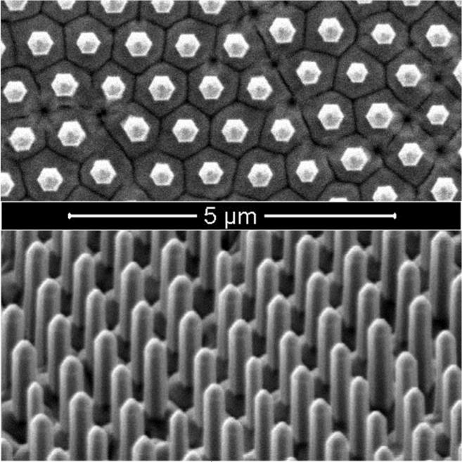
A general overview of the GaN NC arrays is presented in Fig. 2. Figures 2, a and 2, b
show the consistency of the ~1.6 μm tall nanocolumns pre- and post-overgrowth,
respectively. There is some variation in lateral NC size which may result from a
variety of effects including variations in initial nanosphere diameter, inhomogeneities
of the dry ICP and wet KOH-based etches prior to the overgrowth stage (Fig. 2, a) as
well as local growth rate effects due to any array inhomogeneities and initial NC
dimensions. There is some variation in the etch depth of the NCs, of the order of 100
nm, which relates primarily to deeper etching around defects in the NC hexagonal
array. The NC tops are primarily defined by the initial layer growth, which has a
typical root-mean-square roughness, from atomic force microscopy, of less than 1 nm
[33]. The final NC top height variation is not expected to substantially increase as the
wet etch is highly anisotropic (NCs shrink laterally but no c-plane etch happens [34])
and the regrowth conditions (950°C, N2 ambient, high V/III ratio) are chosen to
minimize c-plane growth. Full details on the regrowth procedure will be published
elsewhere [27]; however, the key feature is that the slow c-plane growth is
determined by the fact that if no TMGa is supplied at the applied conditions, there is
a strong decomposition of GaN from c-plane facets of GaN NCs [15]. Supplying of
TMGa during the overgrowth step here simply slows down the decomposition, so that
zero, or even a slightly negative, growth rate is expected for NC c-plane facets.
(a)
(b)
Fig. 2. – SEM micrographs of GaN NC (a) after ~20 hour long KOH-based wet etching
and (b) after an overgrowth at 950°C in nitrogen ambient (upper parts: top view;
bottom parts: 45° tilted view).

6
To investigate the strain state of the different layers of initial GaN templates and GaN
NCs, a separate structure was grown, processed and characterized by XRD. The only
difference from the structure discussed above was an increase in the initial u-GaN
thickness from 200 nm to 500 nm, accompanied by an equivalent decrease in the
thickness of n+-GaN (1500 nm vs. 1800 nm). In Fig. 3, a, a typical symmetric (0004)
2θ–ω XRD reflection curve of the u-GaN/n+-GaN/n–-GaN initial template (curve 1) is
compared to that for the same sample after NC array formation (curve 2).
For the initial template, two peaks are visible, both corresponding to compressively
strained GaN. The lower intensity peak at 2θ = 72.82° can be attributed to the
undoped u-GaN grown directly on the AlN nucleation layer. At the growth
temperature, this layer is expected to be under slight compressive strain due to the
larger a lattice parameter of GaN (3.189 nm), compared to AlN (3.111 nm) [35, 36].
Due to the larger thermal expansion coefficient of sapphire (7.5·10–6 K–1) as compared
to GaN (5.6·10–6 K–1) [37], the u-GaN layer experiences strong compressive strain
upon cooling to room temperature.
The dominant peak at 2θ = 72.89° corresponds to the doped n+ and n– GaN layers.
These layers are under tensile strain at the growth temperature due to doping with
silicon [30, 31, 38] but become slightly compressive on cooldown due to the
GaN/sapphire thermal expansion coefficient difference. Although with reduction of
disilane flow at the n+/n– interface one would also intuitively predict a decrease of
tensile strain in n–-GaN compared to n+-GaN, we do not see splitting of this peak into
two separate ones. Furthermore, no such strain decrease was visible from the in-situ
curvature measurement as the n–-GaN layer was grown.
Upon NC formation (curve 2 in Fig. 3, a), a third peak appears that matches perfectly
with the theoretical value for unstrained GaN. It should be noted that to be able to see
some XRD signal from the nanopatterned material, these data have been obtained for
a sample that was only dry etched (hence the NC array fill factor was significantly
larger than that for the array presented in Fig. 2, a for example). Through removal of
material to form a NC with ICP etching, the pre-existing strain within the NC body is
free to relax, and therefore it is quite reasonable to assign this peak to GaN NCs.
Additionally, the latter is strongly supported from the comparison of 0004 reciprocal
space maps measured before and after formation of NC array (Fig. 3, b and 3, c,
respectively), one can see that the new peak is visibly broader in the horizontal
coordinate corresponding in this case to pure ω angle. By appropriately analyzing
selected linescans from the reciprocal space maps, the rocking curve half-widths for
the dominant peak and additional shoulder have been estimated to be ~80 and ~140
arcsec, respectively. We attribute the broadening of the relaxed GaN peak to small
mutual tilts of the NCs induced by random distribution of the pre-existing dislocations
in and between the NCs, as will be shown in the TEM data.

7
While generation of dislocations at the edges of extra half-planes in materials grown
on non-lattice-matched substrates is an energetically costly process (there is a line
energy associated with a dislocation [39]), it nevertheless occurs as the formation of
the extra half-planes reduces biaxial stress in the structure and thus system total
energy. Upon formation of NCs from dislocated bulk GaN, however, biaxial strain is
free to relax (as seen from the XRD in Fig. 3), and thus the energy associated with
those dislocations still in the NC bodies becomes a non-compensated/excess energy.
The system should be willing to get rid of this energy by reducing the dislocation
lengths. Annealing during the overgrowth step of our fabrication technique can
provide suitable conditions for this process.
72.75 72.80 72.85 72.90 72.95
0.0
0.1
0.2
0.3
0.4
0.5
1
n+/n–-GaN
GaN NCs
I XR
D (
Mcps)
2 (°)
unstrained
GaN(0004) 2 –
u-GaN
2
Fig. 3. – (0004) XRD 2θ–ω scans of a GaN before (curve 1) and after (curve 2) NC array
formation (a) and the corresponding reciprocal space maps (b, c).
The above statement is corroborated by the absence of observable TDs within bodies
of these ‘extremely’ shrunk and then overgrown NCs (see Fig. 4 for a typical example).
Instead of propagating into the NC bodies, TDs tend to bend in the gaps in between
them; as highlighted by arrows in Fig. 4. Although it should be mentioned that the the
number of examined NCs does not allow a statistically meaningful quantitative
estimation regarding the effective TDD for this sample, we conclude that most
dislocations have been removed together with material during the dry etch and
subsequent ‘extreme’ NC shrinkage (as shown in Fig. 2, a). Any residual dislocations
are then bent out of the NCs by the regrowth step, which was carried out at an
elevated temperature (950°C).
To be able to do a more quantitative analysis, another array of NCs was fabricated
where the lateral NC shrinkage prior to overgrowth was somewhat reduced, giving
seed NC diameters of ~200 nm, as opposed to 50-150 nm in the previous case. TEM
analysis on TDs was carried out using the invisibility criterion (gb = 0) with reflective
plane vectors g = ⟨112̅0⟩ and g = ⟨0002⟩. Analysis of Burgers vectors b shows the
majority of dislocations are edge or mixed type, and as expected only a few pure
epi
NC
(b)
(c)
(a)

8
screw-type dislocations were identified. This is consistent with sample data based on
XRD rocking curves.
Fig. 4. – HAADF-STEM image of the GaN NC array upon ‘extreme’ wet etch and lateral
overgrowth. Note the absence of dislocations propagating into the NCs at their base.
Measurements of the dislocation density in the overgrown NCs find a value of
~2.4×107 cm−2 which, taking into account resulting fill-factor of ~30% corresponds to
effective TDD of ~8×107 cm−2. This is both a significant reduction compared to the
aforementioned value of 2×109 cm−2 for an unetched film and the typical reported
literature values. The observed TDD reduction by a factor of about 25 is considerably
higher than the value simply estimated from amount of material removed by
formation and lateral shrinkage of NCs. The latter figure is the ratio of areas of
hexagonal footprint of a NC and its section after wet etch shrinkage. Taking into
account array pitch defined by the initial diameter of SNSs used (≈750 nm) and the
average diameter of GaN NC after their lateral shrinkage by wet etch (≈200 nm), the
proportion of original material in our NCs is estimated to be about 6.5% of total. This
accounts for a factor of about 15.5 improvement in TDD and thus the rest can be
attributed to dislocation bending out of NC bodies into the gaps between the NCs as
shown below.
Various examples of the bending of TDs around the depth corresponding to the NC
bases are shown more detailed in Fig. 5. Unlike in the ‘extremely’ wet etched sample
of Fig. 4, some rare TDs are seen to propagate through to the end of the NC (Fig. 5, a
and 5, e). As already demonstrated in Fig. 1, many TDs will travel to the top of the GaN
film. While the etching stage of NC fabrication will remove a large amount of material
containing TDs; thus, it is expected that some of them will remain within the NCs. Due

9
to the high energy associated with dislocations [40] and vicinity of voids in between
NCs, one could expect that if a dislocation can move it can also bend out of a NC to
reduce the overall system energy. We, however, consider such bending to be possible
only for TDs terminating at NC sidewalls upon their lateral shrinkage. This is further
supported by the absence of dislocations terminating on the sidewalls of all examined
NCs (over ~80 NCs characterized). We believe that all such TDs actually have either
bent out during the wet etch or during the annealing/overgrowth stage. From this
point of view, it is also clear to understand why TDs terminating at the top c-plane
facets of NCs do not seem to bend. First of all, to finally shorten their length by bending
out and migrating with its termination point down to the NC foot, such dislocations
have to increase their length first to reach c-plane/m-plane intersection, for which,
the thermal energy at regrowth conditions may not be sufficient. Secondly
termination points of TDs are often decorated with V-pits [41] and thus can be
strongly pinned to these surface defects.
Aside from the TDs within the NC bodies, it appears that many TDs bend near the top
of the ‘layer’ region just below the start of the NC region. This is clear in Fig. 5, b where
four TDs, two of which appear to be propagating directly into the NCs, bend into the
same region in the middle, in-between the NCs. Analysis of these TDs shows that such
bending occurs in a region 3.0−3.2 µm above the base of the GaN layer which
corresponds to a region ∼ 300 nm below the bottom of the troughs between the NCs.
Fig. 5. – Dark field TEM micrographs of laterally overgrown GaN, demonstrating the
bending of the TDs away from the NCs in the nominally overgrown regions.
The observed dislocation bending differs from that in bottom-up fabricated (grown)
GaN NCs. While completely dislocation-free NCs are claimed only in the case of quite
small diameters (typically ≲100 nm), dislocation filtering is also happening for larger
NCs. However, in this case, dislocation bending happens already within the NC body,

10
typically in its lower part [21, 42] with the propagation height of the dislocations
increasing with NC diameter [21]. Generally, the bending of dislocations is well-
documented in GaN [13, 21], particularly as a result of post-growth thermal annealing
[15] or lateral epitaxial overgrowth [13] where so called image forces are considered
to be the main mechanism for such dislocation movements [43]. From comparison of
the two NC samples here, one can conclude that a dislocation in a GaN NC needs to be
closer than at least 50-70 nm from the surface for image forces to be able to push it
away from NC body. Our estimation matches pretty well with theoretical figure of
about 200 Burgers vectors (~62 nm for edge dislocations in GaN) from the free
surface in a nanocrystal where image forces become essentially non-zero [44]. This
perhaps can explain why no TDs could be observed in our ‘extremely’ wet etched and
overgrown NCs, but a small number of them managed to remain in the sample that
was not so strongly shrunk before overgrowth. This actually might be also the reason
why dislocations simply do not form in bottom-up grown GaN NCs of small enough
diameters [21].
From the TEM analysis it can be then inferred that the rough surface in the areas in-
between NCs (Fig. 2, a) upon annealing/growth stage converts into
thermodynamically stable semipolar {11̅01} facets. These form pedestals at the base
of each NC and valleys, with the deepest regions of no material where adjacent
pedestals intersect. These valleys act as attractors for dislocations (bent out from NC
bodies and those etched away from them) as they minimize TD lengths, compared to
those in the underlying GaN films, and thus the overall system energy. That is the main
reason why most of our NCs are free of dislocations all the way to the NC base.
5 Conclusions
By using a novel hybrid top-down–regrowth method combining MOVPE, ICP etching
with silica nanosphere monolayer as a hard mask, lateral shrinkage with a KOH-based
wet etch and a further lateral overgrowth step, gallium nitride nanocolumns can be
fabricated with a very low dislocation density relative to other current top-down
methods. Transmission electron microscope dark field imaging and analysis of the
threading dislocations shows a directional change as they approach the NCs, bending
into the gaps between them. The analysis confirms that this novel fabrication method
allows for a significant reduction in dislocation density compared to as-grown GaN
films. By implementing an ‘extreme’ lateral shrinkage of NCs (down to diameters of
about 50-150 nm, i.e. just before some initially thinnest NCs may start to disappear)
before overgrowth, it was possible to eliminate dislocations practically completely. In
the other studied case on not so ‘extremely’ shrunk NCs, TDD values of about
2 × 109 cm−2 in bulk layer as compared to 2.4 × 107 cm−2 (8 × 107 cm−2 taking into
account array fill factor) in the overgrown GaN NC arrays have been estimated, giving
improvement factor of about 25. Those NCs with remained dislocations are
nevertheless characterized by sidewall surfaces free of them (the only dislocations
remaining are those completely “buried” in the middle of NC bodies). Taking into

11
account this feature, one can predict that besides using these NCs for applications of
power electronics (the intended use of the present NC arrays was Schottky diodes
[45]), they might be especially promising for optoelectronic devices based on
heterostructures with a core–shell architecture.
6 Acknowledgements
This study was carried out with financial support from Irish Higher Education
Authority Programme for Research in Third Level Institutions Cycles 4 and 5 via the
INSPIRE and TYFFANI projects, Science Foundation Ireland (Grants no. SFI-
13/US/I2860, SFI-18/TIDA/6066), from the Department for the Economy Northern
Ireland under the US-Ireland R&D Partnership Programme (Grant no. USI-058), and
from U.S. National Science Foundation under Grant EECS-1407540. One author (PJP)
acknowledges funding from SFI Engineering Professorship scheme
(SFI/07/EN/E001A). Many thanks to Dr. Martina Luysberg of the Ernst-Ruska Centre,
Forschungszentrum Jülich for access to the CM20 TEM.
References
[1] E. Calleja, M.A. Sánchez-García, F.J. Sánchez, F. Calle, F.B. Naranjo, E. Muñoz, U. Jahn, K. Ploog, Luminescence properties and defects in GaN nanocolumns grown by molecular beam epitaxy, Physical Review B, 62 (2000) 16826-16834. [2] R. Birkhahn, A.J. Steckl, Green emission from Er-doped GaN grown by molecular beam epitaxy on Si substrates, Applied Physics Letters, 73 (1998) 2143-2145. [3] Y. Huang, X. Duan, Y. Cui, C.M. Lieber, Gallium Nitride Nanowire Nanodevices, Nano Letters, 2 (2002) 101-104. [4] Z. Zhong, F. Qian, D. Wang, C.M. Lieber, Synthesis of p-Type Gallium Nitride Nanowires for Electronic and Photonic Nanodevices, Nano Letters, 3 (2003) 343-346. [5] T. Lei, M. Fanciulli, R.J. Molnar, T.D. Moustakas, R.J. Graham, J. Scanlon, Epitaxial growth of zinc blende and wurtzitic gallium nitride thin films on (001) silicon, Applied Physics Letters, 59 (1991) 944-946. [6] D. Doppalapudi, E. Iliopoulos, S.N. Basu, T.D. Moustakas, Epitaxial growth of gallium nitride thin films on A-Plane sapphire by molecular beam epitaxy, Journal of Applied Physics, 85 (1999) 3582-3589. [7] S.W. Lee, D.C. Oh, H. Goto, J.S. Ha, H.J. Lee, T. Hanada, M.W. Cho, T. Yao, S.K. Hong, H.Y. Lee, S.R. Cho, J.W. Choi, J.H. Choi, J.H. Jang, J.E. Shin, J.S. Lee, Origin of forward leakage current in GaN-based light-emitting devices, Applied Physics Letters, 89 (2006) 132117. [8] M.F. Schubert, S. Chhajed, J.K. Kim, E.F. Schubert, D.D. Koleske, M.H. Crawford, S.R. Lee, A.J. Fischer, G. Thaler, M.A. Banas, Effect of dislocation density on efficiency droop in GaInN∕GaN light-emitting diodes, Applied Physics Letters, 91 (2007) 231114. [9] M. Ťapajna, S.W. Kaun, M.H. Wong, F. Gao, T. Palacios, U.K. Mishra, J.S. Speck, M. Kuball, Influence of threading dislocation density on early degradation in AlGaN/GaN high electron mobility transistors, Applied Physics Letters, 99 (2011) 223501. [10] E. Cicek, Z. Vashaei, C. Bayram, R. McClintock, M. Razeghi, M.P. Ulmer, Comparison of ultraviolet APDs grown on free-standing GaN and sapphire substrates, SPIE, 2010. [11] C. Gupta, Y. Enatsu, G. Gupta, S. Keller, U.K. Mishra, High breakdown voltage p–n diodes on GaN on sapphire by MOCVD, physica status solidi (a), 213 (2016) 878-882.
12
[12] D.S. Peng, Y.C. Feng, W.X. Wang, X.F. Liu, W. Shi, H.B. Niu, High-quality GaN films grown on surface treated sapphire substrate, Journal of Physics D: Applied Physics, 40 (2007) 1108-1112. [13] S.E. Bennett, Dislocations and their reduction in GaN, Materials Science and Technology, 26 (2010) 1017-1028. [14] S.D. Lester, F.A. Ponce, M.G. Craford, D.A. Steigerwald, High dislocation densities in high efficiency GaN‐based light‐emitting diodes, Applied Physics Letters, 66 (1995) 1249-1251. [15] M. Conroy, H.N. Li, V.Z. Zubialevich, G. Kusch, M. Schmidt, T. Collins, C. Glynn, R.W. Martin, C. O'Dwyer, M.D. Morris, J.D. Holmes, P.J. Parbrook, Self-Healing Thermal Annealing: Surface Morphological Restructuring Control of GaN Nanorods, Crystal Growth & Design, 16 (2016) 6769-6775. [16] M.J. Kappers, M.A. Moram, Y. Zhang, M.E. Vickers, Z.H. Barber, C.J. Humphreys, Interlayer methods for reducing the dislocation density in gallium nitride, Physica B: Condensed Matter, 401-402 (2007) 296-301. [17] M.A. Moram, Y. Zhang, M.J. Kappers, Z.H. Barber, C.J. Humphreys, Dislocation reduction in gallium nitride films using scandium nitride interlayers, Applied Physics Letters, 91 (2007) 152101. [18] B.A. Haskell, F. Wu, M.D. Craven, S. Matsuda, P.T. Fini, T. Fujii, K. Fujito, S.P. DenBaars, J.S. Speck, S. Nakamura, Defect reduction in (112̄0) a-plane gallium nitride via lateral epitaxial overgrowth by hydride vapor-phase epitaxy, Applied Physics Letters, 83 (2003) 644-646. [19] B.M. Imer, F. Wu, S.P. DenBaars, J.S. Speck, Improved quality (112¯0)a-plane GaN with sidewall lateral epitaxial overgrowth, Applied Physics Letters, 88 (2006) 061908. [20] F. Qian, Y. Li, S. Gradečak, D. Wang, C.J. Barrelet, C.M. Lieber, Gallium Nitride-Based Nanowire Radial Heterostructures for Nanophotonics, Nano Letters, 4 (2004) 1975-1979. [21] K. Kishino, S. Ishizawa, Selective-area growth of GaN nanocolumns on Si(111) substrates for application to nanocolumn emitters with systematic analysis of dislocation filtering effect of nanocolumns, Nanotechnology, 26 (2015) 225602. [22] P.R. Narangari, S.K. Karuturi, M. Lysevych, H.H. Tan, C. Jagadish, Improved photoelectrochemical performance of GaN nanopillar photoanodes, Nanotechnology, 28 (2017) 154001. [23] M. Conroy, V.Z. Zubialevich, H. Li, N. Petkov, J.D. Holmes, P.J. Parbrook, Epitaxial lateral overgrowth of AlN on self-assembled patterned nanorods, Journal of Materials Chemistry C, 3 (2016) 431-437. [24] M. Conroy, V.Z. Zubialevich, H. Li, N. Petkov, S. O'Donoghue, J.D. Holmes, P.J. Parbrook, Ultra-High-Density Arrays of Defect-Free AlN Nanorods: A "Space-Filling" Approach, ACS Nano, 10 (2016) 1988-1994. [25] V.Z. Zubialevich, P. Pampili, M. McLaren, M. Arredondo-Arechavala, G. Sabui, Z. Shen, P.J. Parbrook, Dense GaN nanocolumn arrays by hybrid top-down-regrow approach using nanosphere lithography, in: 2018 IEEE 18th International Conference on Nanotechnology (IEEE-NANO), IEEE, 2018. [26] V.Z. Zubialevich, P. Pampili, M. Akhter, I. Izadi, M. McLaren, M.A. Arechavala, P.J. Parbrook, Dense arrays of GaN nanocolumns fabricated by a hybrid top-down–regrowth method, In preparation, (2020).

13
[27] V.Z. Zubialevich, P. Pampili, P.J. Parbrook, Thermal Stability of Crystallographic Planes of GaN Nanocolumns and Their Lateral Overgrowth by MOVPE, Submitted to Crystal Growth & Design, (2019). [28] U. Martin, U. Mühle, H. Oettel, The Quantitative Measurement of Dislocation Density in the Transmission Electron Microscope, Practical metallography, (1995). [29] A. Pandey, B.S. Yadav, D.V.S. Rao, D. Kaur, A.K. Kapoor, Dislocation density investigation on MOCVD-grown GaN epitaxial layers using wet and dry defect selective etching, Applied Physics A, 122 (2016) 614. [30] A. Dadgar, P. Veit, F. Schulze, J. Bläsing, A. Krtschil, H. Witte, A. Diez, T. Hempel, J. Christen, R. Clos, A. Krost, MOVPE growth of GaN on Si – Substrates and strain, Thin Solid Films, 515 (2007) 4356-4361. [31] K. Forghani, L. Schade, U.T. Schwarz, F. Lipski, O. Klein, U. Kaiser, F. Scholz, Strain and defects in Si-doped (Al)GaN epitaxial layers, Journal of Applied Physics, 112 (2012) 093102. [32] C.G.V.d. Walle, J. Neugebauer, First-principles calculations for defects and impurities: Applications to III-nitrides, Journal of Applied Physics, 95 (2004) 3851-3879. [33] P. Visconti, M.A. Reshchikov, F. Yun, K.M. Jones, H. Morkoç, A. Passaseo, E. Piscopiello, A. Pomarico, R. Cingolani, M. Lomascolo, M. Catalano, Structural, optical and electrical properties of GaN films grown by metalorganic chemical vapor deposition on sapphire, MRS Proceedings, 680 (2011) E3.8. [34] Q. Li, J.B. Wright, W.W. Chow, T.S. Luk, I. Brener, L.F. Lester, G.T. Wang, Single-mode GaN nanowire lasers, Opt. Express, 20 (2012) 17873-17879. [35] V. Darakchieva, B. Monemar, A. Usui, On the lattice parameters of GaN, Applied Physics Letters, 91 (2007) 031911. [36] D. Nilsson, E. Janzén, A. Kakanakova-Georgieva, Lattice parameters of AlN bulk, homoepitaxial and heteroepitaxial material, Journal of Physics D: Applied Physics, 49 (2016) 175108. [37] H. Shin, K. Jeon, Y. Jang, M. Gang, M. Choi, W. Park, K. Park, Comparison of the microstructural characterizations of GaN layers grown on Si (111) and on sapphire, Journal of the Korean Physical Society, 63 (2013) 1621-1624. [38] M.A. Moram, M.J. Kappers, F. Massabuau, R.A. Oliver, C.J. Humphreys, The effects of Si doping on dislocation movement and tensile stress in GaN films, Journal of Applied Physics, 109 (2011) 073509. [39] J. Elsner, R. Jones, P.K. Sitch, V.D. Porezag, M. Elstner, T. Frauenheim, M.I. Heggie, S. Öberg, P.R. Briddon, Theory of Threading Edge and Screw Dislocations in GaN, Physical Review Letters, 79 (1997) 3672-3675. [40] G. Schoeck, The Peierls dislocation: Line energy, line tension, dissociation and deviation, Acta Materialia, 45 (1997) 2597-2605. [41] Z. Chen, L.W. Su, J.Y. Shi, X.L. Wang, C.L. Tang, P. Gao, AFM Application in III-Nitride Materials and Devices, in: V. Bellitto (Ed.) Atomic Force Microscopy, IntechOpen, Rijeka, 2012, pp. 189-208. [42] A. Roshko, M. Brubaker, P. Blanchard, T. Harvey, K.A. Bertness, Selective Area Growth and Structural Characterization of GaN Nanostructures on Si(111) Substrates, Crystals, 8 (2018) 366. [43] W. Ye, A. Ougazzaden, M. Cherkaoui, Analytical formulations of image forces on dislocations with surface stress in nanowires and nanorods, International Journal of Solids and Structures, 50 (2013) 4341-4348.

14
[44] P. Khanikar, A. Kumar, A. Subramaniam, Image forces on edge dislocations: a revisit of the fundamental concept with special regard to nanocrystals, Philosophical Magazine, 91 (2011) 730-750. [45] G. Sabui, V.Z. Zubialevich, M. White, P. Pampili, P.J. Parbrook, M. McLaren, M. Arredondo-Arechavala, Z.J. Shen, GaN Nanowire Schottky Barrier Diodes, IEEE Transactions on Electron Devices, 64 (2017) 2283-2290.