reconfigurable antenna structure for rfid system
TRANSCRIPT
Turk J Elec Eng & Comp Sci, Vol.20, No.4, 2012, c© TUBITAK
doi:10.3906/elk-1004-519
Reconfigurable antenna structure for RFID system
applications using varactor-loading technique
Yusuf SEVINC1, Adnan KAYA2,∗1Department of Electrical and Electronics Engineering, Middle East Technical University,
Ankara-TURKEYe-mail: [email protected]
2Department of Electronics and Communication Engineering, Suleyman Demirel University,32260 Isparta-TURKEY
e-mail: [email protected]
Received: 27.04.2010
Abstract
A novel method is presented for electrically tuning the frequency of a compact radio-frequency iden-
tification (RFID) tag antenna. A tuning circuit, comprising a radio frequency (RF) switch and discrete
passive components, was completely integrated into the antenna element, which is thus free of DC wires. The
low-profile printed antennas were fabricated together with the layouts of the DC control circuits and other
RF/baseband circuit footprints. A surface-mounted varactor was applied as a frequency-tuning element at
the proper places of the meandered slots in the compact antenna. Prototype designs showed that the in-band
frequency (return loss < 10 dB) was tunable from 2.4 GHz to 2.8 GHz when the bias voltage varied from
4 V to 7 V. The impact of the tuning circuit on the antenna’s return loss and radiation pattern were ex-
perimentally studied through comparison with the performance of a reference antenna not incorporating the
tuning circuit. The proposed frequency tuning concept can be extended to more complex compact structures
as well as other types of antennas to give enhanced electrical performance.
Key Words: RFID, Active antenna, frequency tuning, reconfigurable dipole antenna
1. Introduction
In recent years, wireless communication and personal area network technology has grown quickly, especiallyradio-frequency identification (RFID). RFID technology consists of a variety of technologies including theintegrated circuit technique, computer technique, identification technique, and communication technique. Thisworking band of RFID technology covers 100-500 KHz in the low band range, 13.56 MHz in the high band range,and a microwave band range including 860-960 MHz and 2.45 GHz [1]. RFID is a rapidly developing technology
that uses radio frequency (RF) signals for automatic identification of objects. RFID finds many applications invarious areas such as asset identification and retail item management. In RFID systems, the most important
∗Corresponding author: Department of Electrical and Electronics Engineering, Suleyman Demirel University, Isparta-TURKEY
453
Turk J Elec Eng & Comp Sci, Vol.20, No.4, 2012
performance is the maximum read range at which the RFID reader can detect the backscattered signal fromthe tag. The read range is sensitive to the tag orientation, the material on which the tag is placed, and thepropagation environment [2]. It is the antenna that determines the performance of a tag stuck to a specificobject. Therefore, the antenna must be designed and optimized for materials to be attached to it and for arange of locations for these materials. The tag antenna should be small in size, low in profile, and inexpensiveto manufacture. The tag antenna with broadband is also needed to minimize the effect of frequency shift onthe read range, depending on the materials to which it is attached. Compact dipoles or folded dipoles printedon film are being widely studied to comply with these requirements.
A RFID tag is an antenna combined with a microchip in a compact package. Selection of the designedtag antenna with good characteristics for the ultra-high frequency (UHF) and microwave RFID system is a veryimportant project. Dipole-type and patch-type designed antennas allow for RFID tag antenna main use anda modified flexible shape for personal customization. The compact dipole antenna for the RFID tag is a goodcandidate owing to its omnidirectional radiation pattern, simple structure, low cost, and ease of construction.Conventionally, the design shape of the compact antenna from printed microstrip lines, such as folded shapes,meander shapes, and slot-coupled shapes, have attracted increasing attention due to their low profile, reducedsize, and resonance frequency for operating bands [3,4]. However, a fractal shape of technology has beenused to create wide-band or multiband antennas. Several fractal geometries have been introduced for antennaapplication with varying degrees of success in improving antenna characteristics [5]. Some of these geometrieshave been particularly useful in reducing the size of the antenna. These are low-profile antennas with moderategains and they can be operative at multiple frequency bands. The proposed antenna of this study is presentedand explored in 4 stages with the rectangular fractal self-similar rule of shape and metal meander patch, and itcould be applied to the dipole antenna. A wide band characteristic with the fractal improves the narrow bandof the printed compact antenna for RFID application.
In the present study, a model is proposed to analyze the radiation and return loss characteristics of avaractor-loaded compact RFID antenna. Three identical varactor diodes are integrated on the proper placesand edges of a compact antenna. The fringing capacitance introduced at the radiating edge is changed withthe change in the bias voltage, resulting in a change in the electrical length of the patch and thus its resonantfrequency. The resonance of the compact antenna is therefore electronically controlled by the reverse bias ofthe varactor diode.
The analysis of the varactor-loaded compact RFID antenna and radiating-edge gap-coupled parasiticelements is based on circuit theory. The details of the entire investigation are given in the following sections.
2. RFID system overview with theoretical considerations
2.1. Antenna equations
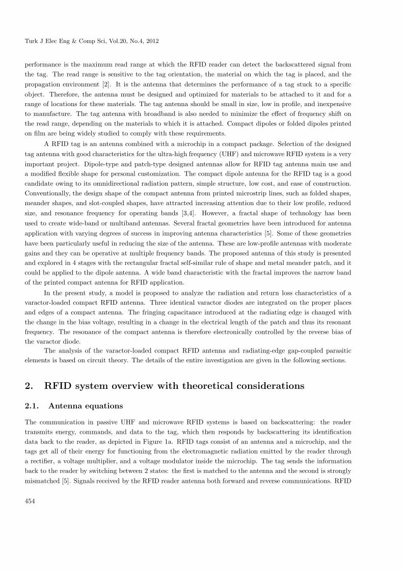
The communication in passive UHF and microwave RFID systems is based on backscattering: the readertransmits energy, commands, and data to the tag, which then responds by backscattering its identificationdata back to the reader, as depicted in Figure 1a. RFID tags consist of an antenna and a microchip, and thetags get all of their energy for functioning from the electromagnetic radiation emitted by the reader througha rectifier, a voltage multiplier, and a voltage modulator inside the microchip. The tag sends the informationback to the reader by switching between 2 states: the first is matched to the antenna and the second is stronglymismatched [5]. Signals received by the RFID reader antenna both forward and reverse communications. RFID
454

SEVINC, KAYA: econfigurable antenna structure for RFID system...,
also normally uses simple modulations such as amplitude-shift keying, phase-shift keying, and frequency-shiftkeying.
Data (Command)
Data (Tag ID)
ReceivingTag AntennaTransmitting
Reader Antenna
R1
ReaderTag/
Transponder
HostComputer
Lf
R L C
Lp
Rs
CT
Cp
PATCH VARACTOR(a) (b)
Figure 1. a. Generic backscattered RFID system. b. Equivalent circuit of varactor-loaded microstrip antenna.
The RF forward communication can be represented as shown in Figure 1a, a block diagram of a typicalRFID system.
The power density at distance R1 from the transmitting antenna in the direction (θ trans , φ trans) is:
Wtrans =PtransGtrans(θtrans, φtrans)
4πR21
(1)
where Ptrans is the input power of the transmitting antenna and Gtrans is the gain of the transmitting readerantenna. PtransGtrans is called the reader-transmitted equivalent isotropic radiated power (EIRP). The power
received by the RFID tag antenna is expressed by the following antenna formula [5]:
Ptag = WtransGtag(θtag , φtag)λ2
4π
∣∣ρ′trans.ρ
′tag
∣∣2
. (2)
The surface waves that flow on the antenna get excited and travel along the dielectric substrate. When thesewaves reach the edges of the substrate, they are reflected, scattered, and diffracted, causing a reduction in gainand an increase in end-fire radiation and cross-polar levels. This also increases the cross-coupling between thearray elements. The excitation of surface waves is a function of εr and h. The power loss in the surface wavesincreases with an increase in the normalized thickness, h/λ0 , of the substrate. The loss due to surface waves
can be neglected when h satisfies the below criterion [6].
h
λ0≤ 0.3
2π√
εr(3)
2.2. Varactor-loaded active compact antenna
The equivalent circuit of a rectangular microstrip antenna is a parallel combination of resistance R , inductanceL , and capacitor C . According to the modal expansion cavity model, the values of R , L , and C are given asbelow [7].
C =ε0εelω
2hcos−2(πd/l) (4)
L =1
ω2C(5)
455
Turk J Elec Eng & Comp Sci, Vol.20, No.4, 2012
R =Qr
ωC(6)
Qr =C√
εr
4fh(7)
Here, c is velocity of light, d is the feed-point location,ω = 2πfr , f r is the design frequency, Qr is the radiationquality factor, and εe is the effective permittivity of the medium. The varactor diode when reverse-biased isshown in Figure 1b, in which Lp and Cp represent the parasitic inductance and capacitance associated withthe mounting and packaging of the device. Rs is the spreading resistance associated with the finite thickness ofthe epitaxial layer as well as the ohmic contact of the diode, and CT is the bias-dependent capacitance, whichis used to obtain the tunable resonance frequency in the microstrip antenna [8,9].
3. Tag antenna structure
This study was simulated on an FR4 substrate with relative permittivity of 4.6, width of 1.6 mm, and dimensions
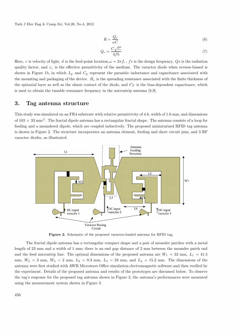
of 103 × 33 mm2 . The fractal dipole antenna has a rectangular fractal shape. The antenna consists of a loop forfeeding and a meandered dipole, which are coupled inductively. The proposed miniaturized RFID tag antennais shown in Figure 2. The structure incorporates an antenna element, feeding and short circuit pins, and 3 RFvaractor diodes, as illustrated.
Figure 2. Schematic of the proposed varactor-loaded antenna for RFID tag.
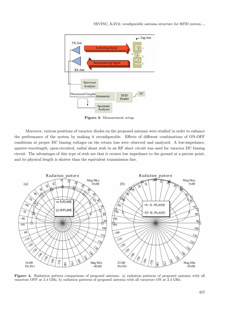
The fractal dipole antenna has a rectangular compact shape and a pair of meander patches with a metallength of 23 mm and a width of 1 mm; there is an end gap distance of 2 mm between the meander patch endand the feed microstrip line. The optimal dimensions of the proposed antenna are W1 = 33 mm, L1 = 41.5mm, W2 = 3 mm, W3 = 2 mm, L2 = 9.3 mm, L3 = 23 mm, and L4 = 15.2 mm. The dimensions of theantenna were first studied with AWR Microwave Office simulation electromagnetic software and then verified bythe experiment. Details of the proposed antenna and results of the prototypes are discussed below. To observethe tag’s response for the proposed tag antenna shown in Figure 2, the antenna’s performances were measuredusing the measurement system shown in Figure 3.
456
SEVINC, KAYA: econfigurable antenna structure for RFID system...,
Figure 3. Measurement setup.
Moreover, various positions of varactor diodes on the proposed antenna were studied in order to enhancethe performance of the system by making it reconfigurable. Effects of different combinations of ON-OFFconditions at proper DC biasing voltages on the return loss were observed and analyzed. A low-impedance,quarter-wavelength, open-circuited, radial shunt stub to an RF short circuit was used for varactor DC biasingcircuit. The advantages of this type of stub are that it creates low impedance to the ground at a precise point,and its physical length is shorter than the equivalent transmission line.
Radia tion_patt er nMag Ma x
10 dB
Mag Min- 40 dB
10 dBPer Di v
E-PLANE
H-PLANE
0-10- 20- 30
- 40
-50- 60
- 70
- 80
-90
- 100
- 110
-120
-130
-140
-150
-160
-170 180
170
160150
140
130
120
110
100
90
80
70
6050
40
30
2010
0-10- 20
30
- 40-50
- 60
- 70
- 80
-90
- 00
- 110
-120
-130
-140
-150
-160
-170 180
170
160150
140
130
120
110
100
90
80
70
6050
40
30
2010
Radia tion_patt er nMag Max
0 dB
Mag Min-50 dB
25 dBPer Div
E -PLANE
H -PLANE
(a) (b)
Figure 4. Radiation pattern comparisons of proposed antenna: a) radiation patterns of proposed antenna with allvaractors OFF at 2.4 GHz, b) radiation patterns of proposed antenna with all varactors ON at 2.4 GHz.
457
Turk J Elec Eng & Comp Sci, Vol.20, No.4, 2012
The performance was measured in terms of the tag antenna’s response, impedance bandwidth, andradiation pattern. Based on the backscattering method, the measurement of the tag antenna was carried out ina clean room. The total measurement system included a transmitting and receiving system. The transmittingsystem consists of a RFID reader (MR3002A) [10] and reader antenna, and it transmits a wake-up signal to thetag antenna. The receiving system consists of a receiving antenna and a spectrum analyzer, and it detects abackscattering signal power from the tag antenna.
4. Experimental results
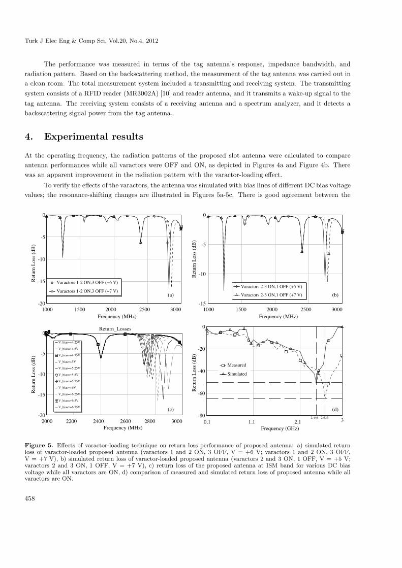
At the operating frequency, the radiation patterns of the proposed slot antenna were calculated to compareantenna performances while all varactors were OFF and ON, as depicted in Figures 4a and Figure 4b. Therewas an apparent improvement in the radiation pattern with the varactor-loading effect.
To verify the effects of the varactors, the antenna was simulated with bias lines of different DC bias voltagevalues; the resonance-shifting changes are illustrated in Figures 5a-5c. There is good agreement between the
1000 1500 2000 2500 3000Frequency (MHz)
-20
-15
-10
-5
0
Ret
urn
Los
s (d
B)
p2p1
Varactors 1-2 ON,3 OFF (+6 V)
Varactors 1-2 ON,3 OFF (+7 V)
1000 1500 2000 2500 3000Frequency (MHz)
-15
-10
-5
0
Ret
urn
Los
s (d
B)
p2p1
Varactors 2-3 ON,1 OFF (+5 V)
Varactors 2-3 ON,1 OFF (+7 V)(a) (b)
2000 2200 2400 2600 2800 3000
(c) (d)
Return_Losses
-20
-15
-10
-5
0p11p10p9p8p7p6p5p4p3p2p1
V_bias=+4.25V
V_bias=+4.5V
V_bias=+4.75V
V_bias=+5V
V_bias=+5.25V
V_bias=+5.5V
V_bias=+5.75V
V_bias=+6V
V_bias=+6.25V
V_bias=+6.5V
V_bias=+6.75V
0.1 1.1 2.1 3
Frequency (GHz)Frequency (MHz)
-80
-60
-40
-20
0
Ret
urn
Los
s (d
B)
Ret
urn
Los
s (d
B)
2.446 2.633
Measured
Simulated
Figure 5. Effects of varactor-loading technique on return loss performance of proposed antenna: a) simulated returnloss of varactor-loaded proposed antenna (varactors 1 and 2 ON, 3 OFF, V = +6 V; varactors 1 and 2 ON, 3 OFF,V = +7 V), b) simulated return loss of varactor-loaded proposed antenna (varactors 2 and 3 ON, 1 OFF, V = +5 V;varactors 2 and 3 ON, 1 OFF, V = +7 V), c) return loss of the proposed antenna at ISM band for various DC biasvoltage while all varactors are ON, d) comparison of measured and simulated return loss of proposed antenna while allvaractors are ON.
458
SEVINC, KAYA: econfigurable antenna structure for RFID system...,
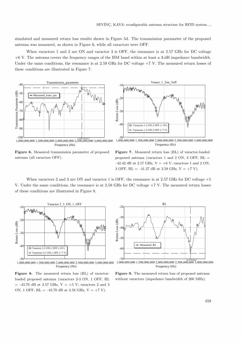
simulated and measured return loss results shown in Figure 5d. The transmission parameter of the proposedantenna was measured, as shown in Figure 6, while all varactors were OFF.
When varactors 1 and 2 are ON and varactor 3 is OFF, the resonance is at 2.57 GHz for DC voltage+6 V. The antenna covers the frequency ranges of the ISM band within at least a 3-dB impedance bandwidth.Under the same conditions, the resonance is at 2.59 GHz for DC voltage +7 V. The measured return losses ofthese conditions are illustrated in Figure 7.
1,000,000,000 1,500,000,000 2,000,000,000 2,500,000,000 3,000,000,000Frequency (Hz)
Transmission_parameter
-100
-90
-80
-70
-60
-50
-40
Tran
smis
sion
Par
amet
er (d
B)
2,438,793,613
Measured_trans. par.
1,000,000,000 1,500,000,000 2,000,000,000 2,500,000,000 3,000,000,000Frequency (Hz)
Varact_1_2on_3off
-50
-40
-30
-20
-10
Ret
urn
Loss
(dB
)
Varactors 1-2 ON,3 OFF (+ 6V)
Varactors 1-2 ON,3 OFF (+7 V)
Figure 6. Measured transmission parameter of proposed
antenna (all varactors OFF).
Figure 7. Measured return loss (RL) of varactor-loaded
proposed antenna (varactors 1 and 2 ON, 3 OFF, RL =
–42.42 dB at 2.57 GHz, V = +6 V; varactors 1 and 2 ON,
3 OFF, RL = –41.27 dB at 2.59 GHz, V = +7 V).
When varactors 2 and 3 are ON and varactor 1 is OFF, the resonance is at 2.57 GHz for DC voltage +5V. Under the same conditions, the resonance is at 2.58 GHz for DC voltage +7 V. The measured return lossesof these conditions are illustrated in Figure 8.
1,000,000,000 1,500,000,000 2,000,000,000 2,500,000,000 3,000,000,000Frequency (Hz)
Varactor 2_3_ON_1_OFF
-50
-40
-30
-20
-10
Ret
urn
Loss
(dB
)
Varactor 2-3 ON,1 OFF (+6V)
Varactors 2-3 ON,1 OFF (+7 V)
1,000,000,000 1,500,000,000 2,000,000,000 2,500,000,000 3,000,000,000Frequency (Hz)
RL
-70
-60
-50
-40
-30
-20
Ret
urn
Loss
(dB
)
2633703920
Measured_RL
Figure 8. The measured return loss (RL) of varactor-
loaded proposed antenna (varactors 2-3 ON, 1 OFF, RL
= –43.70 dB at 2.57 GHz, V = +5 V; varactors 2 and 3
ON, 1 OFF, RL = –43.70 dB at 2.58 GHz, V = +7 V).
Figure 9. The measured return loss of proposed antenna
without varactors (impedance bandwidth of 260 MHz).
459
Turk J Elec Eng & Comp Sci, Vol.20, No.4, 2012
Figure 9 shows the measured return loss of the proposed dipole tag antenna with a gap-coupled-shapedradiator without using varactors. The results of the measurement show that the proposed dipole tag antennaprovides an operation frequency bandwidth of approximately 260 MHz, ranging from 2.48 GHz to 2.74 GHz.Obviously, the proposed design has sufficient bandwidth to meet the requirement of the ISM band’s RFIDapplications.
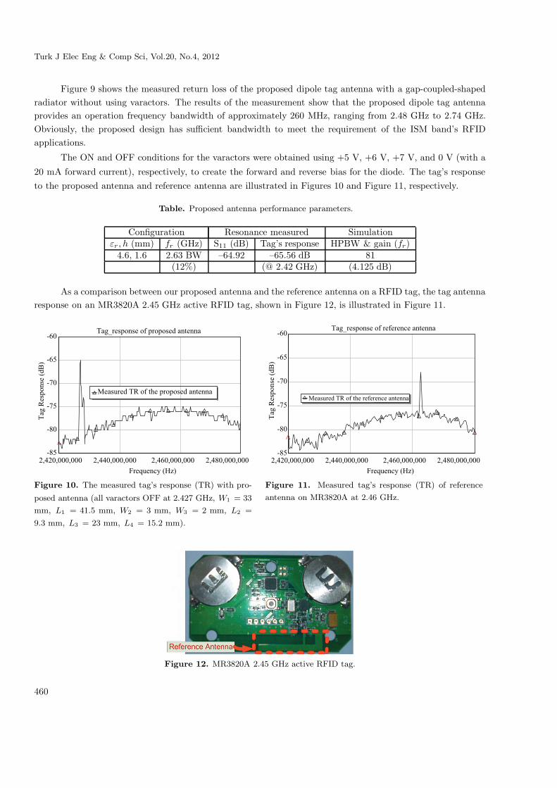
The ON and OFF conditions for the varactors were obtained using +5 V, +6 V, +7 V, and 0 V (with a
20 mA forward current), respectively, to create the forward and reverse bias for the diode. The tag’s responseto the proposed antenna and reference antenna are illustrated in Figures 10 and Figure 11, respectively.
Table. Proposed antenna performance parameters.
Configuration Resonance measured Simulationεr , h (mm) fr (GHz) S11 (dB) Tag’s response HPBW & gain (fr)
4.6, 1.6 2.63 BW –64.92 –65.56 dB 81(12%) (@ 2.42 GHz) (4.125 dB)
As a comparison between our proposed antenna and the reference antenna on a RFID tag, the tag antennaresponse on an MR3820A 2.45 GHz active RFID tag, shown in Figure 12, is illustrated in Figure 11.
2,420,000,000 2,440,000,000 2,460,000,000 2,480,000,000Frequency (Hz)
Tag_response of proposed antenna
-85
-80
-75
-70
-65
-60
Tag
Res
pons
e (d
B)
Measured TR of the proposed antenna
Tag_response of reference antenna
-85
-80
-75
-70
-65
-60
Tag
Res
pons
e (d
B)
Measured TR of the reference antenna
2,420,000,000 2,440,000,000 2,460,000,000 2,480,000,000Frequency (Hz)
Figure 10. The measured tag’s response (TR) with pro-
posed antenna (all varactors OFF at 2.427 GHz, W1 = 33
mm, L1 = 41.5 mm, W2 = 3 mm, W3 = 2 mm, L2 =
9.3 mm, L3 = 23 mm, L4 = 15.2 mm).
Figure 11. Measured tag’s response (TR) of reference
antenna on MR3820A at 2.46 GHz.
Figure 12. MR3820A 2.45 GHz active RFID tag.
460
SEVINC, KAYA: econfigurable antenna structure for RFID system...,
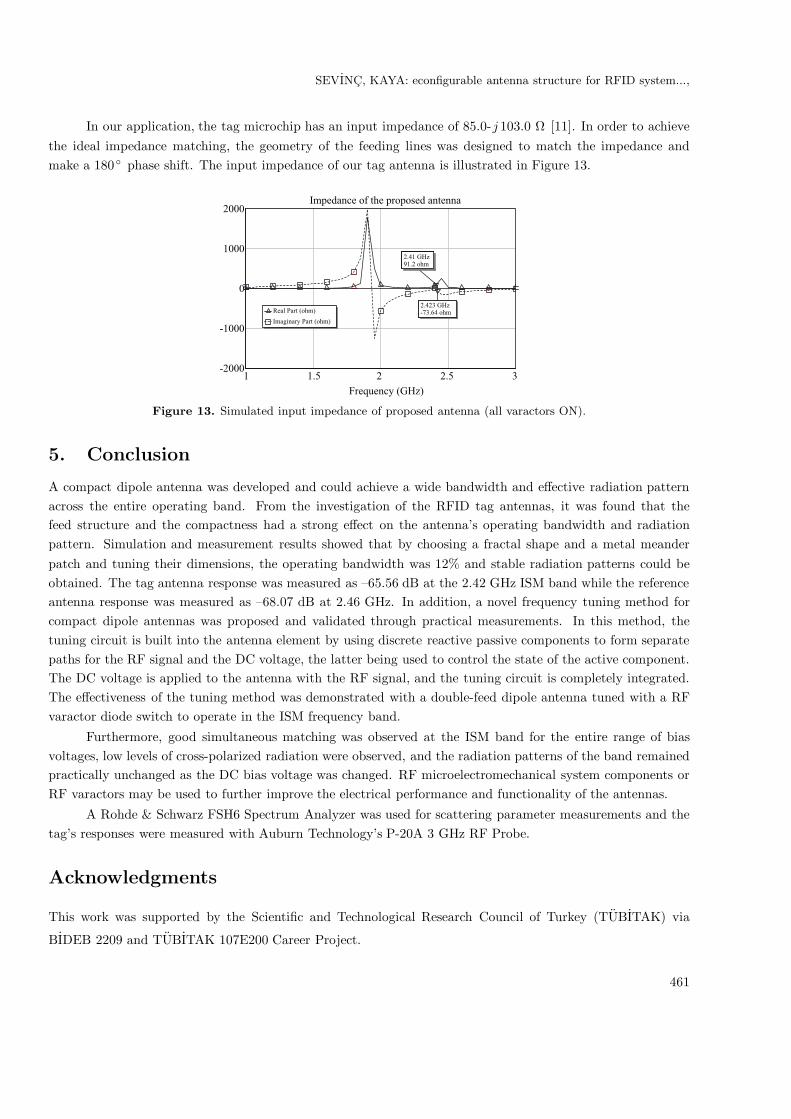
In our application, the tag microchip has an input impedance of 85.0-j 103.0 Ω [11]. In order to achievethe ideal impedance matching, the geometry of the feeding lines was designed to match the impedance andmake a 180◦ phase shift. The input impedance of our tag antenna is illustrated in Figure 13.
1 1.5 2 2.5 3Frequency (GHz)
Impedance of the proposed antenna
-2000
-1000
0
1000
2000
2.423 GHz-73.64 ohm
2.41 GHz91.2 ohm
Real Part (ohm)Imaginary Part (ohm)
Figure 13. Simulated input impedance of proposed antenna (all varactors ON).
5. Conclusion
A compact dipole antenna was developed and could achieve a wide bandwidth and effective radiation patternacross the entire operating band. From the investigation of the RFID tag antennas, it was found that thefeed structure and the compactness had a strong effect on the antenna’s operating bandwidth and radiationpattern. Simulation and measurement results showed that by choosing a fractal shape and a metal meanderpatch and tuning their dimensions, the operating bandwidth was 12% and stable radiation patterns could beobtained. The tag antenna response was measured as –65.56 dB at the 2.42 GHz ISM band while the referenceantenna response was measured as –68.07 dB at 2.46 GHz. In addition, a novel frequency tuning method forcompact dipole antennas was proposed and validated through practical measurements. In this method, thetuning circuit is built into the antenna element by using discrete reactive passive components to form separatepaths for the RF signal and the DC voltage, the latter being used to control the state of the active component.The DC voltage is applied to the antenna with the RF signal, and the tuning circuit is completely integrated.The effectiveness of the tuning method was demonstrated with a double-feed dipole antenna tuned with a RFvaractor diode switch to operate in the ISM frequency band.
Furthermore, good simultaneous matching was observed at the ISM band for the entire range of biasvoltages, low levels of cross-polarized radiation were observed, and the radiation patterns of the band remainedpractically unchanged as the DC bias voltage was changed. RF microelectromechanical system components orRF varactors may be used to further improve the electrical performance and functionality of the antennas.
A Rohde & Schwarz FSH6 Spectrum Analyzer was used for scattering parameter measurements and thetag’s responses were measured with Auburn Technology’s P-20A 3 GHz RF Probe.
Acknowledgments
This work was supported by the Scientific and Technological Research Council of Turkey (TUBITAK) via
BIDEB 2209 and TUBITAK 107E200 Career Project.
461

Turk J Elec Eng & Comp Sci, Vol.20, No.4, 2012
References
[1] K. Finkenzeller, RFID Handbook, 2nd ed., Chichester, Wiley, 2003.
[2] K.V.S. Rao, P.V. Nikitin, S.F. Lam, “Antenna design for UHF RFID tags: A review and a practical application”,
IEEE Transactions on Antennas and Propagation, Vol. 53, pp. 3870-3876, 2005.
[3] A. Ibrahiem, T.P. Vuong, A. Ghiotto, S. Tedjini, “New design antenna for RFID UHF tags”, Proceedings of IEEE
Antennas Propagation Society International Symposium, Albuquerque, pp. 1355-1358, 2006.
[4] S. Jeon, Y. Yu, J. Choi, “Dual-band slot-coupled dipole antenna for 900 MHz and 2.45 GHz RFID tag application”,
Electronics Letters, Vol. 42, pp. 1259-1260, 2006.
[5] Z. Fan, S. Qiao, J.T. Huangfu, L.X. Ran, “Signal descriptions and formulations for long range UHF RFID readers,”
Progress In Electromagnetics Research, Vol. 71, pp. 109-127, 2007.
[6] R. Garg, P. Bhartia, I. Bahl, A. Ittipiboon, Microstrip Antenna Design Handbook, Norwood, Massachusetts, Artech
House, 2001.
[7] I.J. Bahl, P. Bhartia, Microstrip Antennas, Norwood, MA, Artech House, 1980.
[8] M. Komulainen, M. Berg, H. Jantunen, E.T. Salonen, C. Free, “A frequency tuning method for a planar inverted-F
antenna,” IEEE Transactions on Antennas and Propagation, Vol. 56, pp. 944-950, 2008.
[9] R. Boylestad, L. Nashelsky, Electronics Devices and Circuit Theory, 4th ed., New Delhi, Prentice Hall of India,
1989.
[10] Marktrace Technology, “RFID tags”, 2010. Available at http://www.marktrace.com/en/product-default-5.html.
[11] Z. Fan, S. Qiao, J. Huangfu, L. Ran, “A miniaturized 2.45 GHz RFID tag antenna using planar impedance
transformer,” PIERS Online, Vol. 3, pp. 951-954, 2007.
462