recent progress in understanding the electrical ... slides.pdf · recent progress in understanding...
TRANSCRIPT

Recent Progress in Understanding the Electrical Reliability of
GaN High-Electron Mobility Transistors
J. A. del AlamoMicrosystems Technology LaboratoriesMassachusetts Institute of Technology
2015 MRS Spring MeetingSymposium AA: Materials for Beyond the Roadmap Devices in Logic, Power and MemorySan Francisco, CA, April 6-10, 2015
Acknowledgements: C. Y. Chen, F. Gao, J. Jimenez, D. Jin, J. Joh, T. Palacios, C. V. Thompson, Y. WuARL (DARPA-WBGS program), NRO, ONR (DRIFT-MURI program),
Outline
1. A few “universal” observations 2. Hypotheses for degradation mechanisms3. Many questions…
2

Counter-IED Systems (CREW)
200 W GaN HEMT for cellular base station Kawano, APMC 2005
100 mm GaN-on-SiC volume manufacturingPalmour, MTT-S 2010
GaN HEMT: breakthrough RF power technology
Sumitomo Remote Radio Head for
Japanese Base Station3

GaN HEMT: Electrical reliability concerns
High-voltage OFF and semi-ON:– Degradation of IDmax, RD, IGoff
– VT shift– Electron trapping– Trap creation
High-power:– Not accessible to DC stress experiments– Device blows up instantly
ON:– Mostly benign
4
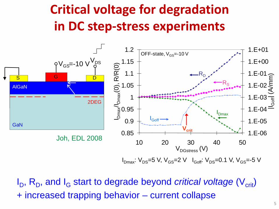
ID, RD, and IG start to degrade beyond critical voltage (Vcrit)+ increased trapping behavior – current collapse
IDmax: VDS=5 V, VGS=2 V IGoff: VDS=0.1 V, VGS=-5 V
Critical voltage for degradation in DC step-stress experiments
Joh, EDL 2008
GS D
AlGaN
GaN
2DEG
VGSVDS
1.E-06
1.E-05
1.E-04
1.E-03
1.E-02
1.E-01
1.E+00
1.E+01
0.85
0.9
0.95
1
1.05
1.1
1.15
1.2
10 20 30 40 50
|I Gof
f| (A
/mm
)
I Dm
ax/I D
max
(0),
R/R
(0)
VDGstress (V)
IDmax
RS
RD
IGoff
Vcrit
OFF-state, VGS=-10 V
=-10 V
5
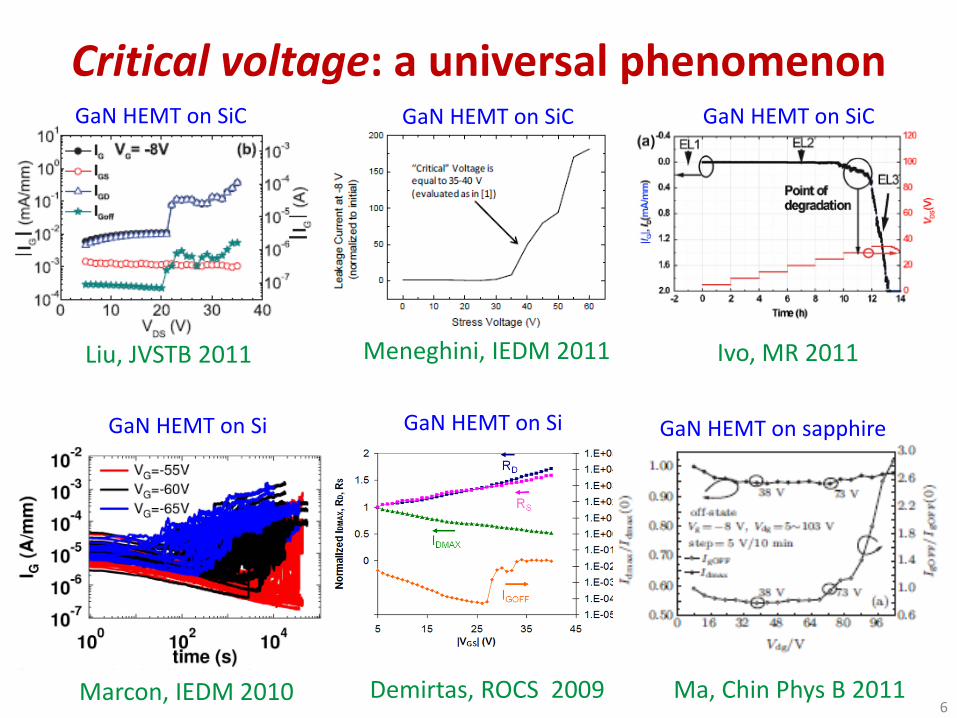
Critical voltage: a universal phenomenon
Meneghini, IEDM 2011 Ivo, MR 2011
GaN HEMT on SiC GaN HEMT on SiC
Demirtas, ROCS 2009
GaN HEMT on Si
Liu, JVSTB 2011
GaN HEMT on SiC
Ma, Chin Phys B 2011
GaN HEMT on sapphire GaN HEMT on Si
Marcon, IEDM 20106

Structural degradation; correlation with electrical degradation
0
10
20
30
40
50
0 2 4 6 8
Perm
anen
t IDm
axDe
grad
atio
n (%
)
Pit depth (nm)
• Pit at edge of gate• Pit depth and IDmax degradation correlate
Pit depth
Joh, MR 2010
Chowdhury, EDL 20087
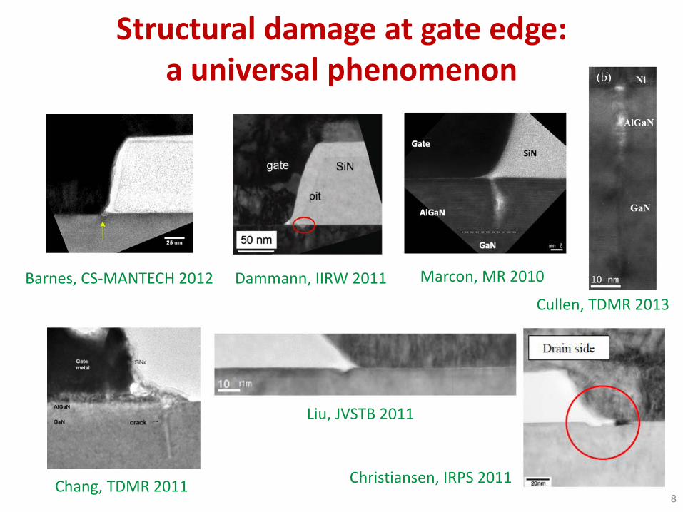
Structural damage at gate edge: a universal phenomenon
Barnes, CS-MANTECH 2012 Dammann, IIRW 2011 Marcon, MR 2010
Chang, TDMR 2011
Liu, JVSTB 2011
Christiansen, IRPS 2011
Cullen, TDMR 2013
8

0
2
4
6
8
10
12
0 50 100 150
Perm
anen
t ID
max
Degr
adat
ion
(%)
Average Defect Area (nm2)
Structural degradation: planar view
200 nm
200 nm
Unstressed
• Vstress>Vcrit: pits along gate edge • Pit cross-sectional area correlates
with ID degradation
OFF-state stress:VDG=57 V, Tbase=150 °C
Makaram, APL 2010
averaged over 1 µm
9
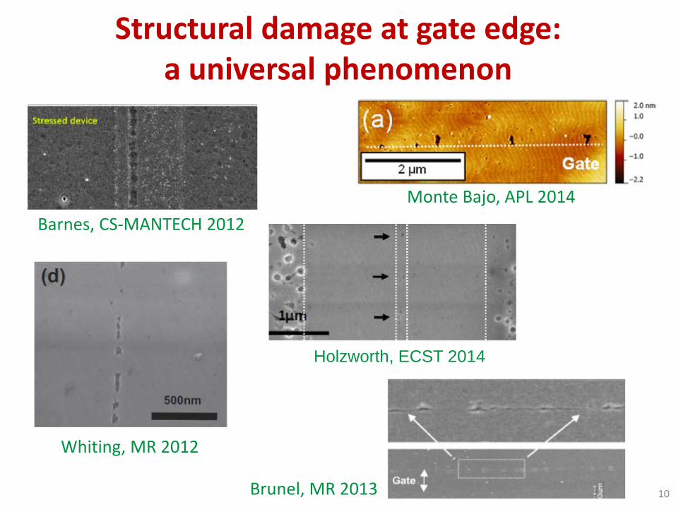
Holzworth, ECST 2014
Structural damage at gate edge: a universal phenomenon
Barnes, CS-MANTECH 2012
Whiting, MR 2012
Brunel, MR 2013
Monte Bajo, APL 2014
10

Time evolution of degradation for constant Vstress > Vcrit
IGoff and VT degradation:• fast (<10 ms)• saturate after 104 s
Permanent IDmax degradation:• much slower• does not saturate with time
10-4 10-2 100 102 104 1060
0.05
0.1
0.15
0.2
0.25
Stress time (s)
|∆V T| (
V)
10-8
10-7
10-6
10-5
10-4
|I Gof
f| (A)
IGoff
|ΔVT|
Initial
Stress: VGS=-7 V and VDS=40 V125 °C
10-4 10-2 100 102 104 1060
0.05
0.1
0.15
0.2
0.25
Stress time (s)
|∆V T| (
V)
10-8
10-7
10-6
10-5
10-4
|I Gof
f| (A)
IGoff
|ΔVT|
Initial
Stress: VGS=-7 V and VDS=40 V125 °C
Joh, IRPS 201111

The role of temperature in time evolution
Different degradation physics:• IG: weak T dependence• IDmax: T activated, Ea similar
to life-test data*
Incubation time
28 30 32 34 36-5
0
5
10
15
1/kT (eV-1)
ln(τ in
c) (s)
Permanent IDmax degradationEa=1.12 eV
Current collapseEa=0.59 eV
IGoff, Ea=0.17 eV
* Saunier, DRC 2007; Meneghesso, IJMWT 2010
Joh, IRPS 2011
Incubation time
12

DC semi-ON stress experiments
• Pits and trenches under gate edge on drain side
• Trench/pit depth and width correlate with IDmax degradation
Stress: ID=100 mA/mm, VDS=40 or 50 V Step-T experiments: 50<Ta<230oC
(Tj~110-330oC)
SEM
AFM
Drain
Wu, JAP 2015
0 5 10 15 20 25 300
10
20
30
40
50
60
70
80
90
Tren
ch/p
it w
idth
, dep
th (n
m)
Permanent IDmax degradation (%)
Trench/pit width
Trench/pit depth
Average of 5 1 µm x1 µm scans at finger center
13

20.0 20.5 21.0 21.5 22.0 22.5 23.0 23.5
4.0
4.5
5.0
5.5
6.0
6.5
7.0
7.5
Ea=1.04 eV
ln(1
/|slo
pe|)
1/kTchannel (eV-1)
• Pit/trench depth increase towards center of gate finger self heating + thermally activated process
• Permanent IDmax degradation thermally activated with Ea~1.0 eV
Wu, MR 2014ΔID=21.6%
Thermally activated degradation
DrainSource
Source
Distance from center of gate finger
Gate fingers
0 20 40 60 80 100 120 140 160 1800.0
0.5
1.0
1.5
2.0
2.5
3.0
3.5
4.0
Dep
th o
f dam
age
(nm
)
Distance from center of gate finger (µm)
ID degradation rate
14
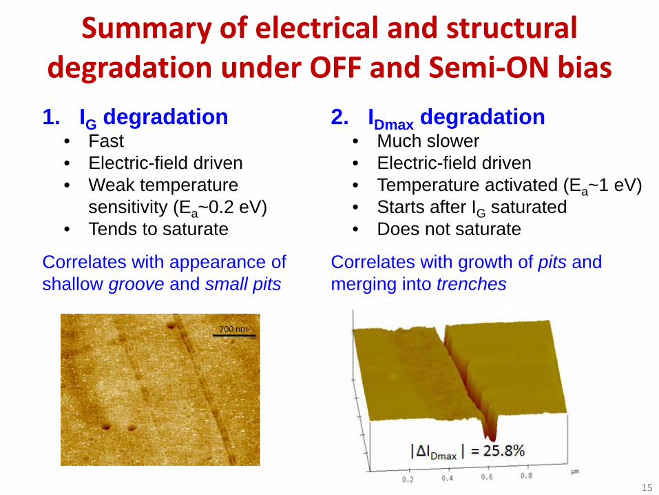
1. IG degradation• Fast• Electric-field driven• Weak temperature
sensitivity (Ea~0.2 eV)• Tends to saturate
Correlates with appearance of shallow groove and small pits
Summary of electrical and structural degradation under OFF and Semi-ON bias
2. IDmax degradation• Much slower• Electric-field driven• Temperature activated (Ea~1 eV)• Starts after IG saturated• Does not saturate
Correlates with growth of pits andmerging into trenches
15
defectstate
ΔΦbi
EC
EF
GS D
AlGaN
GaN2DEG
AlGaN GaN
defectstate
ΔΦbi
EC
EF
GS D
AlGaN
GaN2DEG
AlGaN GaN
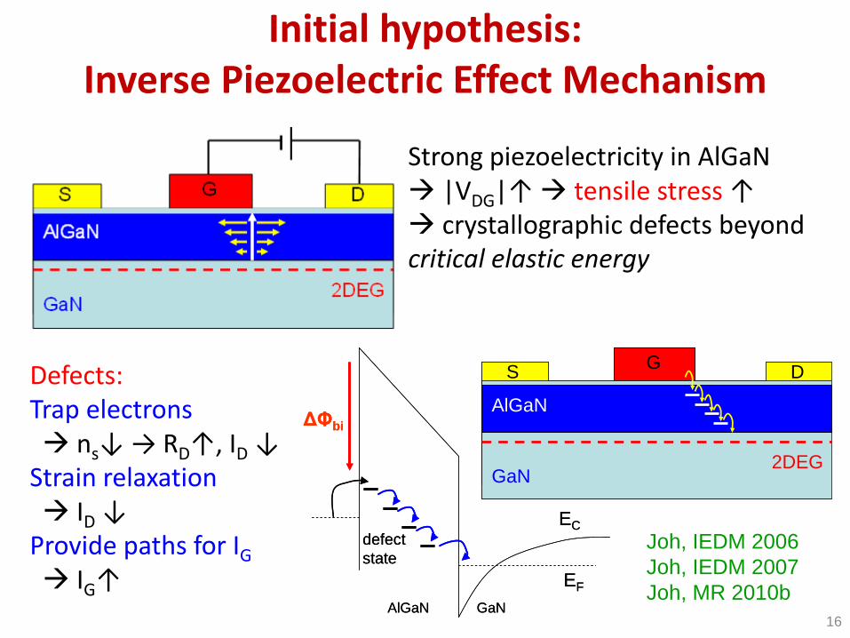
Initial hypothesis: Inverse Piezoelectric Effect Mechanism
Strong piezoelectricity in AlGaN |VDG|↑ tensile stress ↑ crystallographic defects beyond critical elastic energy
Defects:Trap electrons ns↓ → RD↑, ID ↓
Strain relaxation ID ↓
Provide paths for IG IG↑
Joh, IEDM 2006Joh, IEDM 2007Joh, MR 2010b
16
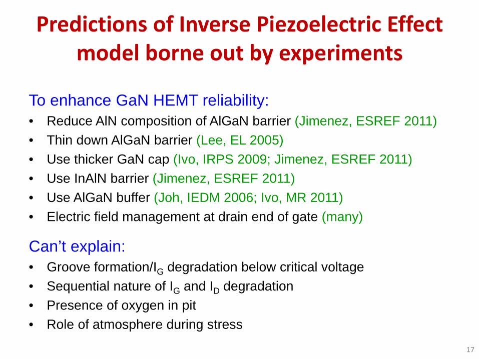
Predictions of Inverse Piezoelectric Effect model borne out by experiments
To enhance GaN HEMT reliability:• Reduce AlN composition of AlGaN barrier (Jimenez, ESREF 2011)• Thin down AlGaN barrier (Lee, EL 2005)• Use thicker GaN cap (Ivo, IRPS 2009; Jimenez, ESREF 2011)• Use InAlN barrier (Jimenez, ESREF 2011)• Use AlGaN buffer (Joh, IEDM 2006; Ivo, MR 2011)• Electric field management at drain end of gate (many)
Can’t explain:• Groove formation/IG degradation below critical voltage • Sequential nature of IG and ID degradation• Presence of oxygen in pit• Role of atmosphere during stress
17

IG degradation not critical; TDDB*-like
Meneghini, IEDM 2011Marcon, IEDM 2010
Vcrit=75 V
• IG starts increasing for Vstress<Vcrit• Onset enhanced by Vstress
• Weibull distribution• Preceded by onset of IG noise
* TDDB = Time-Dependent Dielectric Breakdown18
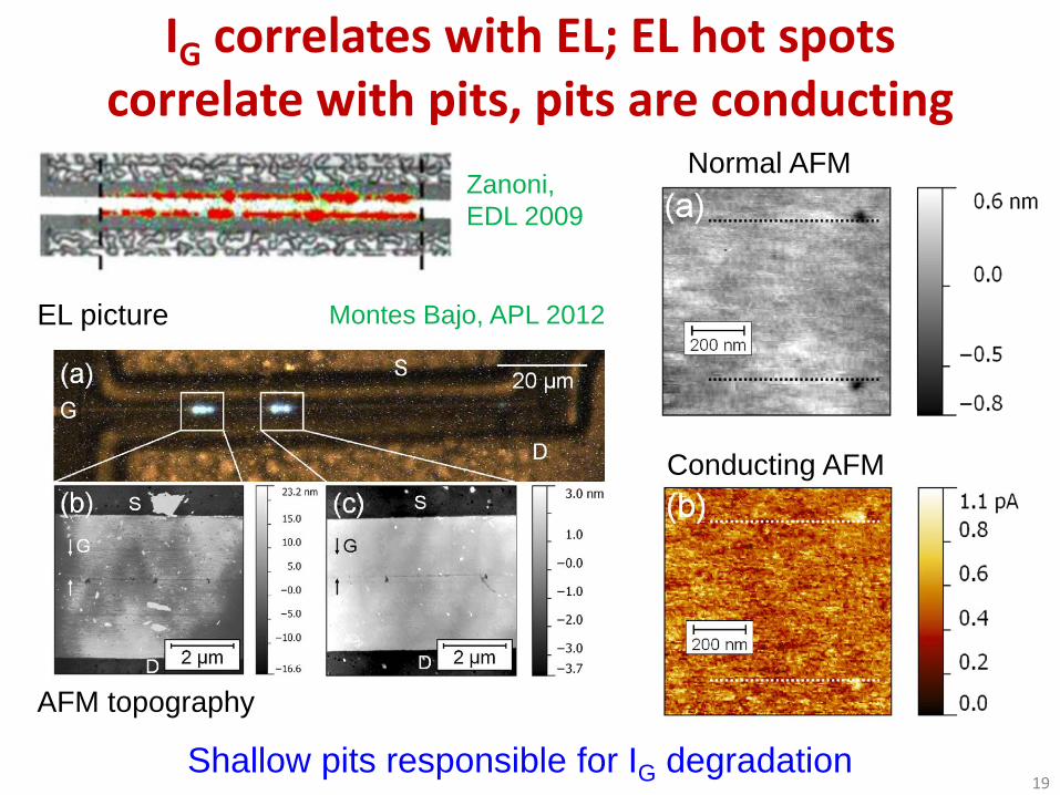
IG correlates with EL; EL hot spots correlate with pits, pits are conducting
Montes Bajo, APL 2012
Shallow pits responsible for IG degradation
Normal AFM
Conducting AFM
EL picture
AFM topography
Zanoni, EDL 2009
19

1E-4 1E-3 0.01 0.1 1 10
0.3
0.4
0.5
0.6
0.7
0.8
0.9
1.0
1.1
I Dm
ax/I D
max
(0)
|IGoff| (mA/mm)
evolution ofstress experiment
“Universal” degradation pattern:• IG degradation first without ID degradation• ID degradation next without further IG degradation• “Corner” of IG and ID same for all samples
Wu, MR 2014
Sequential IG and ID degradation
Semi-ON stress: ID=100 mA/mm, VDS=40 or 50 V Step-Temperature: 50<Ta<230oC
START
Wu, ROCS 2014
20

Oxygen inside pit
• O, Si, C found inside pit• Anodization mechanism for pit
formation? (Smith, ECST 2009)
Park, MR 2009
Conway, Mantech 2007
EDXLEES
21
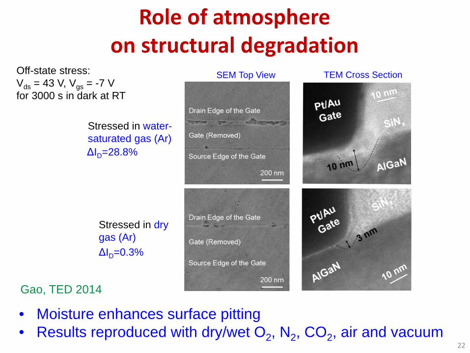
Stressed in water-saturated gas (Ar)
SEM Top View TEM Cross Section
Stressed in dry gas (Ar)
• Moisture enhances surface pitting• Results reproduced with dry/wet O2, N2, CO2, air and vacuum
Gao, TED 2014
ΔID=0.3%
ΔID=28.8%
Off-state stress: Vds = 43 V, Vgs = -7 V for 3000 s in dark at RT
Role of atmosphere on structural degradation
22

New phenomenon: AlGaN corrosion
2AlxGa1-xN + 3H2O ↔ xAl2O3 + (1-x)Ga2O3 + N2 + H2
Electrochemical cell formed at drain edge of gate
Electrochemical reaction (requires holes):
Source of holes: trap-assisted BTBT
Gao, TED 2014
Source of water: diffusion through SiN
23

Tentative complete model? Step 1: formation of shallow pits/continuous groove in cap• TDDB-like formation of small conducting
paths: IG↑
Step 2: growth of pits through anodic oxidation of AlGaN• IDmax↓ as electron concentration under gate
edge reduced
Exponential dependence of tunneling current on electric field origin of “critical voltage” behavior?
200 nmVDG=19 V (Vcrit)
Makaram, APL 2010
200 nmVDG=57 V
24
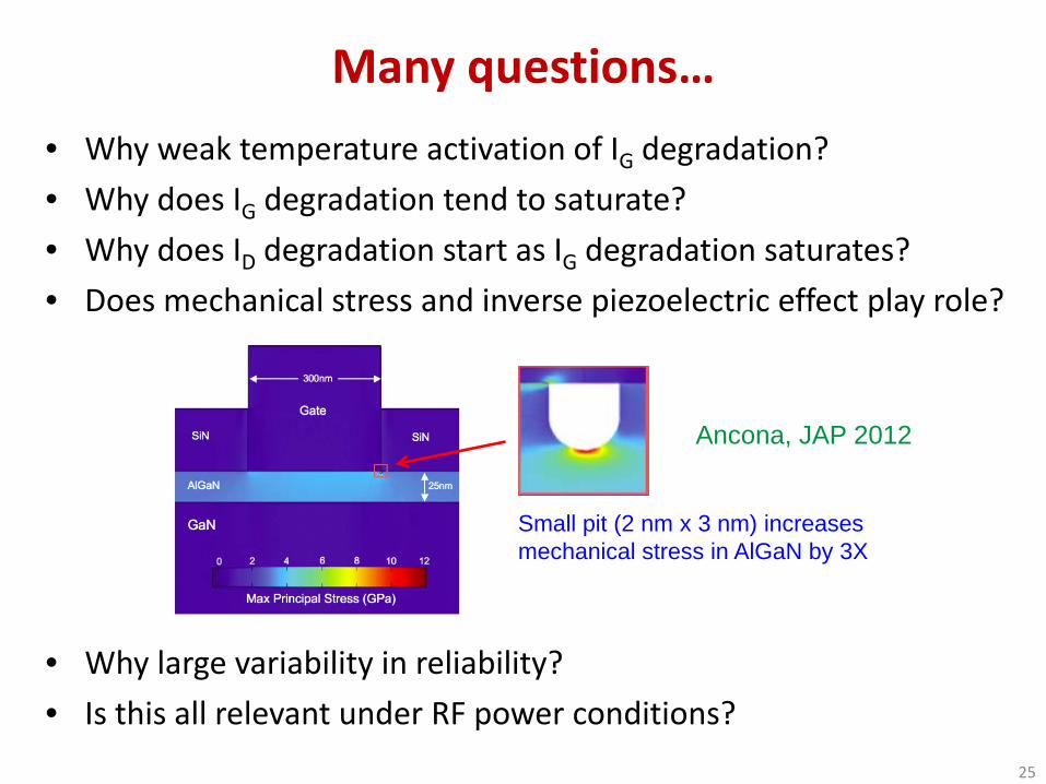
Many questions…• Why weak temperature activation of IG degradation?• Why does IG degradation tend to saturate?• Why does ID degradation start as IG degradation saturates?• Does mechanical stress and inverse piezoelectric effect play role?
• Why large variability in reliability? • Is this all relevant under RF power conditions?
Small pit (2 nm x 3 nm) increases mechanical stress in AlGaN by 3X
Ancona, JAP 2012
25