recent advances in materials and device technologies for
TRANSCRIPT

Recent advances in materials and device technologies for soft active matrix electronics
Journal: Journal of Materials Chemistry C
Manuscript ID TC-REV-05-2020-002160.R2
Article Type: Review Article
Date Submitted by the Author: 23-Jun-2020
Complete List of Authors: Shim, Hyunseok; University of HoustonSim, Kyoseung; University of Houston, Mechanical EngineeringErshad, Faheem; University of Houston, Biomedical EngineeringJang, Seonmin; University of HoustonYu, Cunjiang; University of Houston, Mechanical Engineering
Journal of Materials Chemistry C

1
Recent advances in materials and device technologies for soft active matrix
electronics
Hyunseok Shima, Kyoseung Simb,c, Faheem Ershadd, Seonmin Janga, and Cunjiang Yu*,a,b,d,e
aMaterials Science and Engineering Program, University of Houston, Houston, TX, 77204,
USA
bDepartment of Mechanical Engineering, University of Houston, Houston, TX, 77204 USA
cDepartment of Chemistry, Ulsan National Institute of Science and Technology (UNIST),
Ulsan 44919, Republic of Korea
dDepartment of Biomedical Engineering, University of Houston, Houston, TX, 77204, USA
eDepartment of Electrical and Computer Engineering, Texas Center for Superconductivity,
University of Houston, Houston, TX, 77204, USA
E-mail: [email protected]
Keywords: active matrix, flexible electronics, stretchable electronics, transistors
Page 1 of 35 Journal of Materials Chemistry C

2
Biographies and Pictures:
Hyunseok Shim received his BS in Electronics and Radio Engineering
in 2011 from the Kyung Hee University, and a MS in Physical
Chemistry in 2014 from the Konkuk University, Korea. He was a
researcher in Daegu Gyeongbuk Institute of Science and Technology
(South Korea) from 2014 to 2017. He is currently pursuing Ph.D. degree in Materials Science
and Engineering at University of Houston. His current research focuses on soft electronics.
Dr. Cunjiang Yu is the Bill D. Cook Associate Professor in the
Department of Mechanical Engineering at University of Houston. He
received his Ph.D. degree in Mechanical Engineering from Arizona
State University in 2010. He was a post-doctoral fellow in the
Department of Materials Science and Engineering at University of Illinois at Urbana-
Champaign between 2010 and 2013. He is a recipient of NSF CAREER Award, ONR Young
Investigator Award, MIT Technology Review Top Innovator, AVS Young Investigator Award,
etc. His current research focuses on soft electronics and bioelectronics.
Page 2 of 35Journal of Materials Chemistry C

3
Abstract:
Multiplexed active matrix addressing is critical to extract and process signals from a
large number of channels. Recently, the soft active matrix has attracted a great deal of attention
due to its potential for a variety of applications such as electronic skins, sensors, and
bioelectronics. To realize their use in these various applications, flexible and stretchable
formats of the active matrix technologies have emerged. In this review, a variety of reports on
the soft active matrix are presented and discussed. The technologies of electronic devices
implemented in the modern active matrix are introduced. Strategies to achieve flexible and
stretchable active matrix technologies, their advantages and disadvantages, and their
applications are briefly described. The review closes with a summary, the associated
challenges, and future directions on the development of soft active matrix electronics.
Page 3 of 35 Journal of Materials Chemistry C
4
1. Introduction
Along with the display industry, matrix addressing with both passive and active matrix
technologies have been steadily developed. Early on, passive matrix technologies could be
found in products with liquid crystal displays (LCDs), such as digital clocks and calculators1.
In a passive matrix, each pixel in a grid is defined by the intersecting electrode of the top and
bottom substrates, and a voltage waveform is applied to each pixel to turn the pixels on.
Typically, this requires controlling voltages at the electrical junctions of the grid to turn on a
single pixel, making the response times of the passive matrix slow, and thus, unable to correctly
show rapid motions on a display. Active matrix addressing overcame that limitation through
the attachment of active devices, which serve as switches, to each pixel. Driving the active
devices allows for individual control of pixels2. The concept of active matrix addressing was
first introduced into the literature in 19753. Generally, diodes or transistors serve as the two-
terminal or three-terminal based active devices, respectively4-7. The advancements in active
matrix addressing have allowed the technology utilization to increase beyond the display
industry into various other medical applications such as electronic skins (e-skins), sensors, and
bioelectronics. However, these applications require that the active matrix technologies be made
in compliant formats, that is soft and stretchable, in order to adequately conform to the soft,
curvilinear, and dynamic target surfaces of the human body.
Due to the immense need for wearable and implantable electronic devices in healthcare,
soft electronics, which have been shown to produce conformal contact, accurate measurements,
and enhanced biocompatibility, have been extensively investigated8-11. Examples of soft
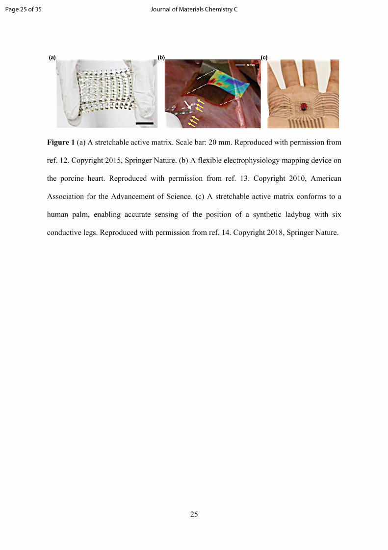
electronics with active matrix technologies are shown in Figure 1. The devices are stretchable
(Figure 1 (a)) and make conformal contact with the moving organs of a mammal (Figure 1
(b)) and a human palm (Figure 1 (c)) to accurately sense the signals12-14.
Approaches to develop conventionally rigid electronics into flexible and stretchable
Page 4 of 35Journal of Materials Chemistry C

5
formats involve reducing the thickness of the electronics and arranging the materials into
structures that can accommodate strain. To make the deformable counterparts to rigid
electronics, strategies of structural engineering of rigid materials, such as pre-straining, in-
plane serpentine, and kirigami has been widely adopted15-17. Furthermore, employing
intrinsically stretchable or rubbery materials has been an alternative strategy to structural
engineering to achieve device stretchability. For instance, electronics in both flexible and
stretchable formats even based on one type of material, such as poly(3,4-
ethylenedioxythiophene)-poly(styrene sulfonate) (PEDOT:PSS), have been developed using
the aforementioned strategies18-27. Alongside the need for wearable and implantable devices is
the requirement for higher spatial resolution to detect signals and resolve features for improved
diagnosis and treatment of health conditions28. A higher density and number of electrodes can
more effectively map tissues/organs of the human body and ultimately improve healthcare
decisions and outcomes29. For these reasons, there has been an emphasis on developing active
matrix technologies using soft electronics.
This review presents an overview of the recent progress in flexible and stretchable
active matrix technologies and discusses their material/device constructions, performances in
the presence of mechanical deformation, and various applications. Specifically, the first section
of this review highlights the advantages/disadvantages of the active matrix, emphasizes the
importance of transistor technologies, and explains the active matrix operation principles. In
the following section, we introduce flexible active matrix electronics that have been
constructed based on arrayed inorganic and organic transistors. Stretchable active matrix
electronics developed with different strategies to achieve stretchability are discussed in the
third section. We conclude with a summary and remarks on the associated challenges in soft
active matrix electronics and possible future directions.
Page 5 of 35 Journal of Materials Chemistry C

6
2. Active matrix
Matrix addressing has been the immediate successor to direct addressing. The
schematic circuit diagram in Figure 2 shows the difference between the two types30-32. Direct
addressing is a method of transmitting signals by connecting all the individual output terminals
of the driver integrated circuit (IC) and to each pixel, as shown in Figure 2 (a). Figure 2 (b)
presents that matrix addressing, including both active and passive matrix addressing, is a
method of transmitting signals to a plurality of pixels using one set of wiring. In terms of the
connection complexity, the number of wires required for direct addressing in an m × n pixel
array is m × n. However, in matrix addressing, only m wires are needed when the data lines are
formed vertically. As a result, matrix addressing has the advantage of significantly reducing
the number of wires compared to direct addressing, which is crucial for minimizing the overall
size of the device and simultaneously allows for higher density and higher resolution arrays.
Furthermore, it is important to consider the differences between the modes of matrix addressing,
namely, passive and active matrix addressing.
In the case of the passive matrix addressing, the signal voltage can affect neighboring
pixels, otherwise known as crosstalk. Therefore, as the number of electrodes increases, the
contrast sharply decreases and the image quality deteriorates. On the other hand, in the case of
active matrix addressing, crosstalk between the pixels can be eliminated since the pixels can
be adjusted by using the active devices. This method guarantees excellent image quality and
displays with high aspect ratios, making the active matrix suitable for high-resolution displays.
Therefore, active matrix addressing is a more advanced method compared to passive matrix
addressing. The slight disadvantage is that the cost to produce this technology is increased
because an active device is used for each pixel, but the tradeoff has been shown to be more
beneficial33.
Figure 3 shows the typical transistor array for active matrix addressing. Active matrix
Page 6 of 35Journal of Materials Chemistry C

7
addressing relies on the stable performance of each pixel. Typically, each pixel consists of
transistors, which are the basic building blocks of electronic circuitry. By ensuring uniform
characteristics of the transistors and rationally arranging them, a reliable active matrix can be
made. The operation principle of an m × n active matrix, particularly in the context of displays,
is described in the following. When the scan line is selected sequentially, it emits light
continuously according to the signal of the data line until the next frame is inputted. For
example, if a circuit operates with passive matrix addressing, n pixels are turned on when the
first gate line is activated. After those n pixels turned off, the second gate line will operate34.
However, if the circuit is operated with active matrix addressing, selected pixels will be turned
on when the first gate line is activated, and the second gate line will be activated before pixels
from the first line are turned off. This occurs because capacitors are connected to the pixels,
allowing for stored information to be kept until the end of one frame so that the image can be
shown correctly6. Again, compared to direct addressing, only m wires are needed when the
data lines are formed vertically, as mentioned above. However, in order to perform the ON/OFF
operation of the switches, wires for controlling the switches are required. This wire is formed
in a direction intersecting the data wiring and simultaneously controls several switches
connected to the wire. Therefore, the number of wires required for driving the active matrix is
the sum of m data lines and n gate lines, which reduces the number of wires that would be
required by direct addressing. It is important to note that gate and data lines are sometimes
referred to as word and bit lines, respectively. In addition, active matrix addressing is suitable
for various applications because the active matrix can be driven at a low voltage and the driving
circuit is inside the matrix, allowing for miniaturization. In the following sections, we have
detailed the flexible and stretchable active matrix technologies and their applications.
Specifically, the associated materials and their applications are summarized in Table 1.
Page 7 of 35 Journal of Materials Chemistry C

8
3. Flexible active matrix
3.1. Flexible active matrix based on inorganic electronics
Recently, active matrix electronics have been developed into flexible formats so that
they can deform or conformally lay on the surfaces of organs and biological tissues. Flexible
active matrix constructed from electronic devices, including diodes and transistors, based on
inorganic semiconductor materials has offered advantages such as higher carrier mobility,
lower operation voltage and improved flexibility, as discussed in the following studies5, 35-53.
Multiple approaches to achieve flexible active matrix devices have been reported, such as
transfer printing inorganic materials (e.g. ultra-thin films and nanowires) on flexible substrates
have been achieved through various process schemes54-59.
Yu et al. developed a flexible multiplexed adaptive optoelectronic camouflage skin
based on ultrathin silicon (Si) diode active matrix5. The camouflage skin pursued a multilayer
configuration with two layers of active matrix electronics: one layer for active matrix based
light sensing and another layer for active matrix based, thermally induced color modulation.
Figure 4 (a) presents a schematic illustration of a 16 × 16 array of interconnected unit cells in
a full, adaptive camouflage skin, where the two layers of the Si diode based active matrix are
employed for light sensing and for thermal actuation. Figure 4 (b) is the schematic illustration
of the sensing part in this system. Distributed active matrix sensing of background patterns was
achieved through arrays of thin Si photodiodes. The photodiodes were positioned at the notches
to allow exposure to the light incident on the system (from above or below) and the
multiplexing blocking diode incorporated an opaque coating to eliminate its sensitivity to light.
A circuit diagram for the sensing part is shown in Figure 4 (c). The voltage pattern that was
obtained from light sensing was used to trigger the thermal actuator pixels accordingly, which
is schematically illustrated in Figure 4 (d). Specifically, an array of ultrathin Si diodes provided
local Joule heating, also with the capability of multiplexed addressing automatically. The active
Page 8 of 35Journal of Materials Chemistry C

9
matrix Si diode based thermal actuator induced changes in the thermochromic materials’ color
in a reflective manner. The circuit diagram for the flexible, diode based active matrix thermal
actuator is presented in Figure 4 (e). The actuation and sensing layers showed excellent
flexibility due to their thin construction. No delamination occurred when the device was bent
to a radius of 2 mm. The maximum strain in silicon depending on the bending radius is shown
in Figure 4 (f). An image of the bent camouflage system is illustrated in Figure 4 (g).
Takei et al. investigated a flexible active matrix based artificial skin using Ge/Si
nanowires (NW) as the active material on a polyimide substrate due to its advantages such as
low operation voltage, superb mechanical robustness, and reliability37. Ge/Si core/shell NW
parallel arrays were transferred to lithographically predefined active regions by a contact-
printing method, as described in detail in elsewhere58, 60. Afterward, a Ni thin film was
deposited to serve as the source and drain electrodes. A schematic exploded view and optical
image of the flexible active matrix based e-skin is presented in Figure 5 (a), which shows
outstanding mechanical flexibility of all integrated components. A single pixel of the active
matrix employed a Ge/Si NW based field effect transistor (FET) that was connected to
pressure-sensitive rubber (PSR) in a 19 × 18 array as shown in Figure 5 (b). The gate and drain
bias of Ge/Si NW FETs were used as the word and bit lines of the active matrix, respectively.
A mapping of the applied pressure was obtained by measuring the conductance of each pixel
in the active matrix. In order to confirm the performance of the flexible active matrix based e-
skin, a ‘C’ shaped PDMS mold was placed on top of e-skin. Figure 5 (c) shows both the design
layout of the active matrix and the corresponding mapping results. Despite a few defective
pixels, the active matrix could clearly map applied pressures.
A flexible inorganic transistor based active matrix can be used not only for e-skin, but
also as a tool for acquiring biological signals. Fang et al. reported a capacitively coupled silicon
array using a silicon nanomembrane based transistor for long-term cardiac electrophysiology46.
Page 9 of 35 Journal of Materials Chemistry C

10
Silicon nanomembranes enable high performance and are compatible with capacitively coupled
systems which are formed by depositing an ultrathin thermal SiO2 layer on top of a Si NMOS
array. Figure 5 (d) shows an exploded view of a completed capacitively coupled flexible
sensing system with an active matrix. The matrix consisted of 18 × 22 capacitive sensors. The
thermally grown SiO2 layer functioned as the dielectric for capacitive coupling between
biological tissue and the semiconducting channels, as well as a barrier layer that hinders the
penetration of bio-fluids. The inset of Figure 5 (d) shows a photograph of the capacitively
coupled sensor array, which shows good flexibility. A circuit diagram for the individual sensor
is shown in Figure 5 (e). Each sensor consisted of an amplifier and a multiplexer with a
capacitive input pad. The signal obtained through the capacitive input pad was transmitted
through an amplifier and was controlled by a multiplexer. A circuit diagram of a common drain
amplifier (source follower) is presented in Figure 5 (f). This circuit provided an optimal
voltage gain of 1 as a result of the large capacitive coupling. The response to the sine wave
input before and after the bending and soaking experiment is shown in Figure 5 (g). The
characterization results from those experimental conditions demonstrated that the device is
suitable for the conditions of the in vivo cardiac environment. Figure 5 (h) shows
electrophysiological signal mapping from a rabbit heart during the sinus rhythm. The results
show that the proposed system can map the electrical signals of the heart with high resolution
while maintaining conformal contact with the heart as shown in the inset of Figure 5 (h).
3.2. Flexible active matrix based on organic electronics
An inorganic material such as Si must be made thin to ensure mechanical flexibility,
which typically involves dedicated microfabrication processes61-64. However, organic materials
which have lower moduli are well suited to be used for flexible electronics. In addition, the
fabrication can be based on relatively simple and low-cost processes as compared to those
Page 10 of 35Journal of Materials Chemistry C

11
utilized with inorganic materials65-67. Many studies have been also reported on the flexible
organic transistor based active matrix4, 68-91. However, the literature has been mainly limited to
displays and there are few reports on other applications92-95. Someya et al. proposed an artificial
skin using an organic semiconductor based flexible pressure sensor matrix in 200468. In this
work, a flexible active matrix was for the first time developed for a pressure sensor array, which
shows many advantages such as low power consumption and less crosstalk. Since then, the
flexible organic semiconductor active matrix has been actively developed for a variety of
applications such as e-skin, sensors, actuators, and memory71, 74, 80, 86-91.
Ren. et al. reported a flexible active matrix for temperature mapping using a
Dinaphthothienothiophene (DNTT) based organic transistor87. A thin ( ~12 μm) poly(ethylene
naphthalate) (PEN) film was used for the substrate which offers high flexibility and bending
stability. Figure 6 (a) shows a schematic illustration of the 16 × 16 array, single pixel, and
circuit diagram. The pentacene/silver nanoparticles (NPs) based thermistor was directly
connected to the drain electrode of an organic transistor for sensing the temperature. Because
the resistance of the thermistor varies depending on temperature, differences in the drain
current could be detected as the temperature changed. To demonstrate its potential for use in
biomedical applications, the active matrix based temperature sensor array was placed on a
human subject's forehead as shown in Figure 6 (b). An advantage of the PEN substrate was
that Vaseline could be added for better contact between the flexible active matrix and the skin.
Figure 6 (c) presents the measured temperature distribution after placing the flexible active
matrix on the forehead which suggests that the device can be used for human body temperature
sensing applications.
Similarly, Sekitani et al. demonstrated the flexible organic transistor based active
matrix for in vivo biological signal mapping (Figure 6 (d))96. To capture weak signals, a small
signal amplifier was constructed using four DNTT-based organic transistors, a resistor, and a
Page 11 of 35 Journal of Materials Chemistry C

12
capacitor connected to the sensing part of the active matrix. Figure 6 (e) shows a circuit
diagram of the flexible active matrix amplifier array. The amplifiers were connected to the
source electrodes of the organic transistor. The active matrix was adhered to skin using
conductive gel. The small signals obtained through the gel were amplified by the amplifier.
Each transistor was controlled by the word line, which enabled the selectively amplified signal
to be received from the bit line. Figure 6 (f, left) shows the photograph of the organic pseudo-
CMOS inverter that was used as the amplifier. To operate the organic pseudo-CMOS inverter,
separate voltages including VDD, VSS, and GND were applied to a circuit of the inverter. The
voltage transfer curve (VTC) and gain of the organic pseudo-CMOS inverter are shown in
Figure 6 (f, right), which shows no obvious degradation before and after being used to contact
a rat heart. The obtained gain from the characterization allows for predicting the degree of
amplification of the small biological signal. Figure 6 (g) presents clear amplification of the
signal attained from the in vivo rat heart.
4. Stretchable active matrix
4.1. Stretchable active matrix based on stretchable interconnects
Although the flexible active matrix has been extensively reported, the stretchable
active matrix has been of great interest as it can accommodate large strain when adhered to
curvy, irregular surfaces and their associated motions12, 14, 97-103. Gray et al. proposed the
island/bridge interconnection approach for inorganic materials based stretchable electronics,
making it possible to construct an active matrix in stretchable formats and enabling a variety
of applications104. Choi et al. reported a Si transistor based stretchable active matrix for a
display based on a similar approach 97. Figure 7 (a) schematically shows a micro-light emitting
diode (µLED) directly connected to a Si transistor in a typical pixel based display. An
intrinsically non-stretchable Au film was patterned in a serpentine shape to ensure stretchability
Page 12 of 35Journal of Materials Chemistry C

13
and was utilized as the interconnects between the rigid island pixels and circuitry in the active
matrix. The circuit diagram of the active matrix is shown in Figure 7 (b). As discussed earlier
in Figure 2, the circuit structure is a typical transistor array for multiplexed active matrix
addressing. When the gate signal was sequentially selected, the µLED emitted light according
to a data signal. Figure 7 (c) shows the dynamic operation of the active matrix on a
polydimethylsiloxane (PDMS) substrate. The active matrix display was used to depict the word
“YONSEI” by changing the gate and data lines in real time. The active matrix display
functioned normally with no cracks or line disconnection under a mechanical strain of 40% as
shown in Figure 7 (d). The shape of the letter “N” remained discernable under mechanical
strain and the light emission was uniform (no degradation) because of the strain
accommodation by the mechanically deformed serpentine shaped stretchable interconnects
(Figure 7 (e)).
Architectural engineering of stretchable interconnects involves sophisticated
fabrication processes and low integration density, which limits the applications of electronics
developed using those strategies. An alternative strategy for the stretchable active matrix
involves using intrinsically stretchable interconnects with rigid islands based active
electronics12, 98-102.
Sekitani et al. reported a stretchable active matrix using a single wall carbon nanotube
(SWNT) elastic conductor and paste based stretchable interconnects98. Pentacene was used as
the organic semiconductor for transistors fabricated on a polyimide substrate, which is not
stretchable, as shown in Figure 8 (a). Taking advantage of the SWNT elastic conductor and
paste, 19 × 37 organic transistors based stretchable active matrix with stretchable SWNT
interconnection was fabricated. Each transistor was placed on silicone rubber and the elastic
conductor and paste were implemented for the interconnects, word lines, and bit lines. A
schematic illustration of the stretchable active matrix is shown in Figure 8 (b). The active
Page 13 of 35 Journal of Materials Chemistry C

14
matrix shows no cracks or damages at 70% biaxial stretching, as pictured in Figure 8 (c). In
addition, no significant degradation of the device performance was observed (Figure 8 (d))
which implies that the active matrix using rigid islands and intrinsically stretchable
interconnection is mechanically and electrically stable under biaxial strain.
Liquid metal is another potential promising candidate for interconnects of stretchable
electronics because it remains conductive even under a mechanical strain of ~ 300%105, 106.
Park et al. reported a stretchable active matrix using liquid metal for interconnects and IGZO
as the semiconductor for the rigid island transistor on a polyimide substrate101. Here, the liquid
metal was patterned by a photolithography-based technique compatible with conventional
flexible circuit technology to form the interconnects. Figure 8 (e) shows the optical microscope
image and schematic cross-sectional view of the IGZO based transistor. To demonstrate the
benefit of using liquid metal, a 4 × 4 active matrix array based on IGZO transistors was
fabricated and mechanically and electrically characterized. The circuit diagram of the active
matrix is shown in Figure 8 (f, left). Liquid metal was used for the interconnects, including the
bit, data, and GND lines. The combination of rigid transistors and liquid metal interconnects
functioned stably under a mechanical deformation of 40% as shown in Figure 8 (f, right). In
addition, the transfer characteristics of the oxide transistor showed no change under a
mechanical strain of 40%, as shown in Figure 8 (g).
4.2. Stretchable active matrix all based on intrinsically stretchable, rubbery electronics
The approach of using rigid islands and stretchable interconnects to create the
stretchable active matrix is promising, but some disadvantages remain. Since stretchable
interconnects are required between transistor units, there is a trade-off between device density
and stretchability. Also, the manufacturing process is complicated and not compatible with
fully solution processable fabrication methods. Recently, another strategy for implementing a
Page 14 of 35Journal of Materials Chemistry C

15
stretchable active matrix has been enabled by the use of all rubber-like intrinsically stretchable
materials (e.g. rubbery semiconductor, conductor, and gate dielectric) for fabricating
stretchable transistors14, 103, 107-109. This approach has excellent advantages such as high
mechanical stability, simple device structure for the active matrix, and easy fabrication in a
solution processable manner14, 103. Thus, efforts have been made to develop the intrinsically
stretchable active matrix based on such stretchable transistors.
Wang et al. produced a tactile sensing skin based on an intrinsically stretchable active
matrix. The transistors in the 10 × 10 active matrix were constructed using all stretchable
materials, including a polymeric semiconductor/elastomer composite (29-DPP-
SVS/polystyrene-block-poly(ethylene-ran-butylene)-block-polystyrene (SEBS)), SEBS, and
CNT as the stretchable semiconductor, gate dielectric, and conductor, respectively. The
transistors showed stable operation under a mechanical strain of 100%14. The intrinsically
stretchable active matrix for tactile sensing was constructed by connecting the drain electrode
of the transistor to the resistive tactile sensor for each pixel. In addition, a scan line and a data
line were connected to the gate electrode and the source electrode, respectively, as shown in
Figure 9 (a). When the resistance of the tactile sensor was altered by physical touching, a
voltage was applied to the drain electrode and current flowed accordingly, depending on the
gate voltage. One of the primary advantages of the intrinsically stretchable active matrix is that
a separate structural design is not required to fabricate a stretchable active matrix because all
the materials that compose the active matrix are intrinsically stretchable. Figure 9 (b) shows
the image of the stretchable active matrix and the inset shows the transfer characteristics of a
single transistor. The high stretchability of the active matrix allows it to be attached
conformally to the human palm. Figure 9 (c) shows an optical image of an artificial ladybug
that was placed on the tactile sensing active matrix and the corresponding tactile mapping,
which indicates the detected pressure from the six legs of the ladybug. The results showed the
Page 15 of 35 Journal of Materials Chemistry C

16
feasibility of a stretchable active matrix as a backplane for high-resolution tactile sensing.
Sim et al. recently reported a fully rubbery active matrix for tactile sensing skin using
high performance rubbery transistors based on a multi-wall carbon nanotube (CNT) doped
poly(3-hexylthiophene) nanofibril (P3HT-NF)/PDMS composite as the semiconducting
material103. Figure 9 (d) shows the circuit diagram of a single pixel of the stretchable active
matrix based tactile sensing skin, which was constructed by connecting the rubbery transistors
and PSR based tactile sensors. The tactile sensors had a very low resistance under applied
pressure, but without pressure, the sensors had high resistance, and thus the drain voltage could
be applied to the rubbery transistor. By selectively controlling the word line, current flowed
accordingly through the bit line. This current was then detected as a voltage across a resistor
which was appropriately chosen. When the drain voltage of -1 V was applied to the transistor,
an output of -1 V was measured once the tactile sensor was pressed. Figure 9 (e) shows the
deformed fully rubbery active matrix under mechanical stretching. In order to confirm that the
proposed fully rubbery active matrix functioned as a tactile sensing skin, an arbitrarily shaped
object was placed on top of the active matrix. Figure 9 (f) shows the voltage mapping results
before and after applying mechanical strain of 30% along the channel length direction and no
significant difference in mapping results before and after stretching was observed.
5. Summary, Challenges, and Outlook
5.1. Summary
Multiplexed active matrix addressing has been successfully implemented for a variety
of applications, however, numerous challenges still need to be overcome. For example, there
are many reports on rigid and flexible active matrix technologies, but there are limited reports
on stretchable active matrix technologies partially because they are more difficult to realize.
Of course, the results for existing flexible active matrix demonstrate that they can serve as
Page 16 of 35Journal of Materials Chemistry C

17
electronic skins, sensors, and bioelectronics, but further research on stretchable active matrix
technologies is urgently required to match the increasing needs in wearable, portable,
stretchable and implantable electronics.
5.2. Challenges
Some representative challenges to develop soft active matrix technologies are as
follows. For instance, even though there are a few existing reports on stretchable active matrix
technologies, typically the driving voltages are fairly high98, 101, which poses biosafety issues
for biomedical applications14, 110. In other words, low operation voltages for stretchable active
matrix technologies are needed103, 109. In addition, the next generation of wearable and
implantable devices urgently requires high spatiotemporal resolution. Therefore, further
studies on intrinsically stretchable, rubbery electronics are required to enable high spatial
resolution (high density). In addition, the operation speed of the transistors also needs to
increase to enable high temporal resolution. As mentioned before, the stretchable active matrix
all based on intrinsically stretchable, rubbery transistors does not require a separate structural
design (which requires large areas for interconnects) and thus, it can be used to implement a
higher density of devices14. Simultaneously, issues such as poor stability and relatively low
carrier mobility which are generally associated with the use of organic electronic materials
need to be resolved111, 112. Manufacturing technologies to pattern intrinsically stretchable
semiconductors, conductors, and dielectrics must be improved for precise patterning at the
micro/nanoscale113-117. To simultaneously realize high mechanical strain tolerance and
electrical performances is also essential, which requires a deep understanding of the structure-
property relationships between electronic materials and their mechanical and electrical
properties118. Furthermore, the rational integration of the soft active matrix with sensors of high
sensitivity, conformability, and biocompatibility is another consideration for accurate and
Page 17 of 35 Journal of Materials Chemistry C

18
precise biological signal acquisition from tissues such as the heart, muscle, and brain tissues.
5.3. Outlook
Although many challenges remain, future research and development in active matrix
addressing technology and its applications are promising. Due to its soft mechanical attributes,
the soft active matrix can be investigated and employed for further applications where a large
number of signals are extracted from soft objects such as human and animal bodies, organs,
tissues, and machine interfaces devices among others13, 38, 46, 88, 96.
Page 18 of 35Journal of Materials Chemistry C

19
Conflicts of interest
The authors declare no competing financial interests.
Acknowledgements
C.Y. would like to thank the National Science Foundation CAREER grant (CMMI-1554499),
the Doctoral New Investigator grant from American Chemical Society Petroleum Research
Fund (56840-DNI7), and the Office of Naval Research grant (N00014-18-1-2338) under
Young Investigator Program.
Page 19 of 35 Journal of Materials Chemistry C

20
Notes and references
1. L. Goodman, IEEE Transactions on Consumer Electronics, 1975, 247-259.2. W. F. Aerts, S. Verlaak and P. Heremans, IEEE Trans. Electron Devices, 2002, 49,
2124-2130.3. T. Brody, F. C. Luo, Z. P. Szepesi and D. H. Davies, IEEE Trans. Electron Devices,
1975, 22, 739-748.4. N. Matsuhisa, H. Sakamoto, T. Yokota, P. Zalar, A. Reuveny, S. Lee and T. Someya,
Advanced Electronic Materials, 2016, 2, 1600259.5. C. Yu, Y. Li, X. Zhang, X. Huang, V. Malyarchuk, S. Wang, Y. Shi, L. Gao, Y. Su
and Y. Zhang, Proceedings of the National Academy of Sciences, 2014, 111, 12998-13003.
6. M. L. Chabinyc and A. Salleo, Chem. Mater., 2004, 16, 4509-4521.7. G. Gelinck, P. Heremans, K. Nomoto and T. D. Anthopoulos, Adv. Mater., 2010, 22,
3778-3798.8. D.-H. Kim, Y.-S. Kim, J. Amsden, B. Panilaitis, D. L. Kaplan, F. G. Omenetto, M. R.
Zakin and J. A. Rogers, Applied physics letters, 2009, 95, 133701.9. J. Reeder, M. Kaltenbrunner, T. Ware, D. Arreaga‐Salas, A. Avendano‐Bolivar, T.
Yokota, Y. Inoue, M. Sekino, W. Voit and T. Sekitani, Adv. Mater., 2014, 26, 4967-4973.
10. K. Fukuda, Y. Takeda, Y. Yoshimura, R. Shiwaku, L. T. Tran, T. Sekine, M. Mizukami, D. Kumaki and S. Tokito, Nat. Commun., 2014, 5, 4147.
11. D. Son, J. Lee, S. Qiao, R. Ghaffari, J. Kim, J. E. Lee, C. Song, S. J. Kim, D. J. Lee and S. W. Jun, Nat. Nanotechnol., 2014, 9, 397.
12. N. Matsuhisa, M. Kaltenbrunner, T. Yokota, H. Jinno, K. Kuribara, T. Sekitani and T. Someya, Nature communications, 2015, 6, 7461.
13. J. Viventi, D.-H. Kim, J. D. Moss, Y.-S. Kim, J. A. Blanco, N. Annetta, A. Hicks, J. Xiao, Y. Huang and D. J. Callans, Science translational medicine, 2010, 2, 24ra22-24ra22.
14. S. Wang, J. Xu, W. Wang, G.-J. N. Wang, R. Rastak, F. Molina-Lopez, J. W. Chung, S. Niu, V. R. Feig and J. Lopez, Nature, 2018, 555, 83-88.
15. X. Feng, B. D. Yang, Y. Liu, Y. Wang, C. Dagdeviren, Z. Liu, A. Carlson, J. Li, Y. Huang and J. A. Rogers, Acs Nano, 2011, 5, 3326-3332.
16. C. Dagdeviren, Y. Shi, P. Joe, R. Ghaffari, G. Balooch, K. Usgaonkar, O. Gur, P. L. Tran, J. R. Crosby and M. Meyer, Nat. Mater., 2015, 14, 728.
17. M. Isobe and K. Okumura, Scientific reports, 2016, 6, 24758.18. W. Lee and T. Someya, Chemistry of Materials, 2019, 31, 6347-6358.19. X. Fan, W. Nie, H. Tsai, N. Wang, H. Huang, Y. Cheng, R. Wen, L. Ma, F. Yan and
Y. Xia, Advanced Science, 2019, 6, 1900813.20. L. V. Kayser and D. J. Lipomi, Advanced Materials, 2019, 31, 1806133.21. H. Yuk, B. Lu, S. Lin, K. Qu, J. Xu, J. Luo and X. Zhao, Nature communications,
2020, 11, 1-8.22. D. J. Lipomi and Z. Bao, Energy & Environmental Science, 2011, 4, 3314-3328.23. R. Zhou, P. Li, Z. Fan, D. Du and J. Ouyang, Journal of Materials Chemistry C, 2017,
5, 1544-1551.24. M. Y. Teo, N. Kim, S. Kee, B. S. Kim, G. Kim, S. Hong, S. Jung and K. Lee, ACS
applied materials & interfaces, 2017, 9, 819-826.25. W. Lee, D. Kim, N. Matsuhisa, M. Nagase, M. Sekino, G. G. Malliaras, T. Yokota
and T. Someya, Proceedings of the National Academy of Sciences, 2017, 114, 10554-
Page 20 of 35Journal of Materials Chemistry C

21
10559.26. J. H. Lee, Y. R. Jeong, G. Lee, S. W. Jin, Y. H. Lee, S. Y. Hong, H. Park, J. W. Kim,
S.-S. Lee and J. S. Ha, ACS applied materials & interfaces, 2018, 10, 28027-28035.27. K. Yamagishi, T. Nakanishi, S. Mihara, M. Azuma, S. Takeoka, K. Kanosue, T.
Nagami and T. Fujie, NPG Asia Materials, 2019, 11, 1-13.28. F. Ershad, K. Sim, A. Thukral, Y. S. Zhang and C. Yu, APL Materials, 2019, 7,
031301.29. A. M. Taplin, A. de Pesters, P. Brunner, D. Hermes, J. C. Dalfino, M. A. Adamo, A.
L. Ritaccio and G. Schalk, Epilepsy & behavior case reports, 2016, 5, 46-51.30. P. A. Ersman, J. Kawahara and M. Berggren, Org. Electron., 2013, 14, 3371-3378.31. X. Zhang, P. Li, X. Zou, J. Jiang, S. H. Yuen, C. W. Tang and K. M. Lau, IEEE
Photonics Technology Letters, 2019, 31, 865-868.32. T. N. Ruckmongathan, Addressing techniques of liquid crystal displays, John Wiley
& Sons, 2014.33. T. Sekitani and T. Someya, Adv. Mater., 2010, 22, 2228-2246.34. H. Kubota, S. Miyaguchi, S. Ishizuka, T. Wakimoto, J. Funaki, Y. Fukuda, T.
Watanabe, H. Ochi, T. Sakamoto and T. Miyake, J. Lumin., 2000, 87, 56-60.35. J.-S. Park, T.-W. Kim, D. Stryakhilev, J.-S. Lee, S.-G. An, Y.-S. Pyo, D.-B. Lee, Y.
G. Mo, D.-U. Jin and H. K. Chung, Applied Physics Letters, 2009, 95, 013503.36. J.-S. Yoo, S.-H. Jung, Y.-C. Kim, S.-C. Byun, J.-M. Kim, N.-B. Choi, S.-Y. Yoon,
C.-D. Kim, Y.-K. Hwang and I.-J. Chung, Journal of display technology, 2010, 6, 565-570.
37. K. Takei, T. Takahashi, J. C. Ho, H. Ko, A. G. Gillies, P. W. Leu, R. S. Fearing and A. Javey, Nat. Mater., 2010, 9, 821.
38. J. Viventi, D.-H. Kim, L. Vigeland, E. S. Frechette, J. A. Blanco, Y.-S. Kim, A. E. Avrin, V. R. Tiruvadi, S.-W. Hwang and A. C. Vanleer, Nat. Neurosci., 2011, 14, 1599.
39. T. Takahashi, K. Takei, A. G. Gillies, R. S. Fearing and A. Javey, Nano Lett., 2011, 11, 5408-5413.
40. C. Wang, D. Hwang, Z. Yu, K. Takei, J. Park, T. Chen, B. Ma and A. Javey, Nat. Mater., 2013, 12, 899.
41. T. Takahashi, Z. Yu, K. Chen, D. Kiriya, C. Wang, K. Takei, H. Shiraki, T. Chen, B. Ma and A. Javey, Nano Lett., 2013, 13, 5425-5430.
42. J. T. Smith, B. O'Brien, Y.-K. Lee, E. J. Bawolek and J. B. Christen, Journal of Display Technology, 2014, 10, 514-520.
43. Q. Sun, W. Seung, B. J. Kim, S. Seo, S. W. Kim and J. H. Cho, Adv. Mater., 2015, 27, 3411-3417.
44. C. Yeom, K. Chen, D. Kiriya, Z. Yu, G. Cho and A. Javey, Adv. Mater., 2015, 27, 1561-1566.
45. X. Cao, C. Lau, Y. Liu, F. Wu, H. Gui, Q. Liu, Y. Ma, H. Wan, M. R. Amer and C. Zhou, ACS nano, 2016, 10, 9816-9822.
46. H. Fang, K. J. Yu, C. Gloschat, Z. Yang, E. Song, C.-H. Chiang, J. Zhao, S. M. Won, S. Xu and M. Trumpis, Nature biomedical engineering, 2017, 1, 0038.
47. J. Li, E. Song, C.-H. Chiang, K. J. Yu, J. Koo, H. Du, Y. Zhong, M. Hill, C. Wang and J. Zhang, Proceedings of the National Academy of Sciences, 2018, 115, E9542-E9549.
48. M. Choi, Y. J. Park, B. K. Sharma, S.-R. Bae, S. Y. Kim and J.-H. Ahn, Sci. Adv., 2018, 4, eaas8721.
49. L. Nela, J. Tang, Q. Cao, G. Tulevski and S.-J. Han, Nano Lett., 2018, 18, 2054-2059.
Page 21 of 35 Journal of Materials Chemistry C

22
50. T.-Y. Zhao, D. Zhang, T.-Y. Qu, L.-L. Fang, Q.-B. Zhu, Y. Sun, T.-H. Cai, M. Chen, B.-W. Wang and J. Du, ACS. Appl. Mater. Interfaces., 2019, 11, 11699.
51. Y. J. Park, B. K. Sharma, S. M. Shinde, M.-S. Kim, B. Jang, J.-H. Kim and J.-H. Ahn, ACS nano, 2019, 13, 3023-3030.
52. J. Jang, B. Oh, S. Jo, S. Park, H. S. An, S. Lee, W. H. Cheong, S. Yoo and J. U. Park, Advanced Materials Technologies, 2019, 4, 1900082.
53. R. Yao, Z. Zheng, M. Xiong, X. Zhang, X. Li, H. Ning, Z. Fang, W. Xie, X. Lu and J. Peng, Applied Physics Letters, 2018, 112, 103503.
54. M. C. McAlpine, H. Ahmad, D. Wang and J. R. Heath, Nature materials, 2007, 6, 379-384.
55. J. A. Rogers and Y. Huang, Proceedings of the National Academy of Sciences, 2009, 106, 10875-10876.
56. J. Yoon, A. J. Baca, S.-I. Park, P. Elvikis, J. B. GEDDES III, L. Li, R. H. Kim, J. Xiao, S. Wang and T.-H. Kim, in Materials for Sustainable Energy: A Collection of Peer-Reviewed Research and Review Articles from Nature Publishing Group, World Scientific, 2011, pp. 38-46.
57. A. Javey, S. Nam, R. S. Friedman, H. Yan and C. M. Lieber, Nano letters, 2007, 7, 773-777.
58. Z. Fan, J. C. Ho, Z. A. Jacobson, R. Yerushalmi, R. L. Alley, H. Razavi and A. Javey, Nano letters, 2008, 8, 20-25.
59. H. Ning, Y. Zeng, Y. Kuang, Z. Zheng, P. Zhou, R. Yao, H. Zhang, W. Bao, G. Chen and Z. Fang, ACS Applied Materials & Interfaces, 2017, 9, 27792-27800.
60. Z. Fan, J. C. Ho, Z. A. Jacobson, H. Razavi and A. Javey, Proceedings of the National Academy of Sciences, 2008, 105, 11066-11070.
61. D. Shahrjerdi and S. W. Bedell, Nano Lett., 2012, 13, 315-320.62. F. Giacomozzi, V. Mulloni, S. Colpo, J. Iannacci, B. Margesin and A. Faes,
Romanian Journal of Information Science and Technology (ROMJIST), 2011, 14, 259-268.
63. H. Qu, Micromachines, 2016, 7, 14.64. J.-H. Seo, K. Zhang, M. Kim, W. Zhou and Z. Ma, npj Flexible Electronics, 2017, 1,
1.65. S. Logothetidis, Materials Science and Engineering: B, 2008, 152, 96-104.66. B. C.-K. Tee, A. Chortos, A. Berndt, A. K. Nguyen, A. Tom, A. McGuire, Z. C. Lin,
K. Tien, W.-G. Bae and H. Wang, Science, 2015, 350, 313-316.67. T. W. Kelley, P. F. Baude, C. Gerlach, D. E. Ender, D. Muyres, M. A. Haase, D. E.
Vogel and S. D. Theiss, Chemistry of Materials, 2004, 16, 4413-4422.68. T. Someya, T. Sekitani, S. Iba, Y. Kato, H. Kawaguchi and T. Sakurai, Proceedings
of the National Academy of Sciences, 2004, 101, 9966-9970.69. S. Burns, K. Reynolds, W. Reeves, M. Banach, T. Brown, K. Chalmers, N. Cousins,
M. Etchells, C. Hayton and K. Jacobs, Journal of the Society for Information Display, 2005, 13, 583-586.
70. H. Kawaguchi, T. Someya, T. Sekitani and T. Sakurai, IEEE Journal of Solid-State Circuits, 2005, 40, 177-185.
71. T. Someya, Y. Kato, T. Sekitani, S. Iba, Y. Noguchi, Y. Murase, H. Kawaguchi and T. Sakurai, Proceedings of the National Academy of Sciences, 2005, 102, 12321-12325.
72. L. Zhou, A. Wanga, S.-C. Wu, J. Sun, S. Park and T. N. Jackson, Applied Physics Letters, 2006, 88, 083502.
73. M. Mizukami, N. Hirohata, T. Iseki, K. Ohtawara, T. Tada, S. Yagyu, T. Abe, T.
Page 22 of 35Journal of Materials Chemistry C

23
Suzuki, Y. Fujisaki and Y. Inoue, IEEE Electron Device Lett., 2006, 27, 249-251.74. Y. Noguchi, T. Sekitani and T. Someya, Applied physics letters, 2006, 89, 253507.75. Y. Kato, T. Sekitani, M. Takamiya, M. Doi, K. Asaka, T. Sakurai and T. Someya,
IEEE Trans. Electron Devices, 2007, 54, 202-209.76. P. Andersson, R. Forchheimer, P. Tehrani and M. Berggren, Adv. Funct. Mater.,
2007, 17, 3074-3082.77. I. Yagi, N. Hirai, Y. Miyamoto, M. Noda, A. Imaoka, N. Yoneya, K. Nomoto, J.
Kasahara, A. Yumoto and T. Urabe, Journal of the Society for Information Display, 2008, 16, 15-20.
78. T. Sekitani, T. Yokota, U. Zschieschang, H. Klauk, S. Bauer, K. Takeuchi, M. Takamiya, T. Sakurai and T. Someya, Science, 2009, 326, 1516-1519.
79. T. Sekitani, U. Zschieschang, H. Klauk and T. Someya, Nat. Mater., 2010, 9, 1015.80. K. Fukuda, T. Sekitani, U. Zschieschang, H. Klauk, K. Kuribara, T. Yokota, T.
Sugino, K. Asaka, M. Ikeda and H. Kuwabara, Adv. Funct. Mater., 2011, 21, 4019-4027.
81. M. Zirkl, A. Sawatdee, U. Helbig, M. Krause, G. Scheipl, E. Kraker, P. A. Ersman, D. Nilsson, D. Platt and P. Bodö, Adv. Mater., 2011, 23, 2069-2074.
82. T. Yokota, T. Sekitani, T. Tokuhara, N. Take, U. Zschieschang, H. Klauk, K. Takimiya, T.-C. Huang, M. Takamiya and T. Sakurai, IEEE Trans. Electron Devices, 2012, 59, 3434-3441.
83. J. Kawahara, P. Andersson Ersman, D. Nilsson, K. Katoh, Y. Nakata, M. Sandberg, M. Nilsson, G. Gustafsson and M. Berggren, J. Polym. Sci., Part B: Polym. Phys., 2013, 51, 265-271.
84. M. Kaltenbrunner, T. Sekitani, J. Reeder, T. Yokota, K. Kuribara, T. Tokuhara, M. Drack, R. Schwödiauer, I. Graz and S. Bauer-Gogonea, Nature, 2013, 499, 458.
85. B. Peng, X. Ren, Z. Wang, X. Wang, R. C. Roberts and P. K. Chan, Scientific reports, 2014, 4, 6430.
86. T. Yokota, Y. Inoue, Y. Terakawa, J. Reeder, M. Kaltenbrunner, T. Ware, K. Yang, K. Mabuchi, T. Murakawa and M. Sekino, Proceedings of the National Academy of Sciences, 2015, 112, 14533-14538.
87. X. Ren, K. Pei, B. Peng, Z. Zhang, Z. Wang, X. Wang and P. K. Chan, Adv. Mater., 2016, 28, 4832-4838.
88. W. Lee, D. Kim, J. Rivnay, N. Matsuhisa, T. Lonjaret, T. Yokota, H. Yawo, M. Sekino, G. G. Malliaras and T. Someya, Adv. Mater., 2016, 28, 9722-9728.
89. S. Lee, A. Reuveny, J. Reeder, S. Lee, H. Jin, Q. Liu, T. Yokota, T. Sekitani, T. Isoyama and Y. Abe, Nat. Nanotechnol., 2016, 11, 472.
90. K. Pei, X. Ren, Z. Zhou, Z. Zhang, X. Ji and P. K. L. Chan, Adv. Mater., 2018, 30, 1706647.
91. M. Kondo, M. Melzer, D. Karnaushenko, T. Uemura, S. Yoshimoto, M. Akiyama, Y. Noda, T. Araki, O. Schmidt and T. Sekitani, Science advances, 2020, 6, eaay6094.
92. G. H. Gelinck, H. E. A. Huitema, E. Van Veenendaal, E. Cantatore, L. Schrijnemakers, J. B. Van Der Putten, T. C. Geuns, M. Beenhakkers, J. B. Giesbers and B.-H. Huisman, Nat. Mater., 2004, 3, 106.
93. C. Sheraw, L. Zhou, J. Huang, D. Gundlach, T. Jackson, M. Kane, I. Hill, M. Hammond, J. Campi and B. Greening, Applied physics letters, 2002, 80, 1088-1090.
94. Y.-H. Kim, S.-K. Park, D.-G. Moon, W.-K. Kim and J.-I. Han, Displays, 2004, 25, 167-170.
95. P. Mach, S. Rodriguez, R. Nortrup, P. Wiltzius and J. A. Rogers, Applied Physics Letters, 2001, 78, 3592-3594.
Page 23 of 35 Journal of Materials Chemistry C

24
96. T. Sekitani, T. Yokota, K. Kuribara, M. Kaltenbrunner, T. Fukushima, Y. Inoue, M. Sekino, T. Isoyama, Y. Abe and H. Onodera, Nat. Commun., 2016, 7, 11425.
97. M. Choi, B. Jang, W. Lee, S. Lee, T. W. Kim, H. J. Lee, J. H. Kim and J. H. Ahn, Adv. Funct. Mater., 2017, 27, 1606005.
98. T. Sekitani, Y. Noguchi, K. Hata, T. Fukushima, T. Aida and T. Someya, Science, 2008, 321, 1468-1472.
99. T. Sekitani, H. Nakajima, H. Maeda, T. Fukushima, T. Aida, K. Hata and T. Someya, Nat. Mater., 2009, 8, 494.
100. S. Y. Hong, Y. H. Lee, H. Park, S. W. Jin, Y. R. Jeong, J. Yun, I. You, G. Zi and J. S. Ha, Adv. Mater., 2016, 28, 930-935.
101. C. W. Park, J. B. Koo, C.-S. Hwang, H. Park, S. G. Im and S.-Y. Lee, Applied Physics Express, 2018, 11, 126501.
102. D. S. Kim, H. Park, S. Y. Hong, J. Yun, G. Lee, J. H. Lee, L. Sun, G. Zi and J. S. Ha, Appl. Surf. Sci., 2019, 471, 300-308.
103. K. Sim, Z. Rao, H.-J. Kim, A. Thukral, H. Shim and C. Yu, Science advances, 2019, 5, eaav5749.
104. D. S. Gray, J. Tien and C. S. Chen, Adv. Mater., 2004, 16, 393-397.105. Q. Gao, H. Li, J. Zhang, Z. Xie, J. Zhang and L. Wang, Scientific reports, 2019, 9,
5908.106. Y. Yang, N. Sun, Z. Wen, P. Cheng, H. Zheng, H. Shao, Y. Xia, C. Chen, H. Lan and
X. Xie, ACS nano, 2018, 12, 2027-2034.107. J. Y. Oh, S. Rondeau-Gagné, Y.-C. Chiu, A. Chortos, F. Lissel, G.-J. N. Wang, B. C.
Schroeder, T. Kurosawa, J. Lopez and T. Katsumata, Nature, 2016, 539, 411.108. H.-J. Kim, K. Sim, A. Thukral and C. Yu, Sci. Adv., 2017, 3, e1701114.109. H. Shim, K. Sim, F. Ershad, P. Yang, A. Thukral, Z. Rao, H.-J. Kim, Y. Liu, X. Wang
and G. Gu, Science advances, 2019, 5, eaax4961.110. J. Xu, S. Wang, G.-J. N. Wang, C. Zhu, S. Luo, L. Jin, X. Gu, S. Chen, V. R. Feig and
J. W. To, Science, 2017, 355, 59-64.111. A. F. Paterson, S. Singh, K. J. Fallon, T. Hodsden, Y. Han, B. C. Schroeder, H.
Bronstein, M. Heeney, I. McCulloch and T. D. Anthopoulos, Advanced Materials, 2018, 30, 1801079.
112. X. Jia, C. Fuentes-Hernandez, C.-Y. Wang, Y. Park and B. Kippelen, Science advances, 2018, 4, eaao1705.
113. M. J. Kim, M. Lee, H. Min, S. Kim, J. Yang, H. Kweon, W. Lee, D. H. Kim, J.-H. Choi and D. Y. Ryu, Nature communications, 2020, 11, 1-11.
114. E. K. Lee, C. H. Park, J. Lee, H. R. Lee, C. Yang and J. H. Oh, Advanced Materials, 2017, 29, 1605282.
115. J. A. DeFranco, B. S. Schmidt, M. Lipson and G. G. Malliaras, Organic Electronics, 2006, 7, 22-28.
116. H. Minemawari, T. Yamada, H. Matsui, J. y. Tsutsumi, S. Haas, R. Chiba, R. Kumai and T. Hasegawa, Nature, 2011, 475, 364-367.
117. H. Sirringhaus, T. Kawase, R. Friend, T. Shimoda, M. Inbasekaran, W. Wu and E. Woo, Science, 2000, 290, 2123-2126.
118. Z. Bao and X. Chen, Advanced Materials, 2016, 28, 4177-4179.
Page 24 of 35Journal of Materials Chemistry C
25
Figure 1 (a) A stretchable active matrix. Scale bar: 20 mm. Reproduced with permission from
ref. 12. Copyright 2015, Springer Nature. (b) A flexible electrophysiology mapping device on
the porcine heart. Reproduced with permission from ref. 13. Copyright 2010, American
Association for the Advancement of Science. (c) A stretchable active matrix conforms to a
human palm, enabling accurate sensing of the position of a synthetic ladybug with six
conductive legs. Reproduced with permission from ref. 14. Copyright 2018, Springer Nature.
Page 25 of 35 Journal of Materials Chemistry C

26
Figure 2 Schematic diagram of (a) direct addressing and (b) matrix addressing.
Page 26 of 35Journal of Materials Chemistry C

27
Figure 3 Typical transistor array for active matrix addressing.
Page 27 of 35 Journal of Materials Chemistry C

28
Figure 4 (a) Exploded view of illustration of a 16×16 array of interconnected unit cells in a
full, adaptive camouflage skin. (b) The schematic exploded view of sensing part includes a
photodiode and a multiplexing (blocking) diode connected in a back-to-back fashion. (c) A
circuit diagram for sensing part. (d) The schematic exploded view of heating part with
multiplexed addressing. (e) A circuit diagram for heating part. (f) Maximum strain in silicon
depending on the bending radius. (g) Image of a device in operation while bent, while showing
the text pattern “U o I”. Reproduced with permission from ref. 5. Copyright 2014, National
Academy of Sciences.
Page 28 of 35Journal of Materials Chemistry C

29
Figure 5 (a) An exploded view of a flexible active matrix based e-skin. (b) Optical microscope
image of a single sensor pixel in the array (left) and circuitry of active matrix (right). (c) Design
layout of the active matrix (left) and the corresponding mapping results from pixel signals
(right). Reproduced with permission from ref. 37. Copyright 2010, Springer Nature. (d) An
exploded view of a completed capacitively coupled flexible sensing system. (e) A circuit
diagram for each sensor. (f) A circuit of a common drain amplifier (source follower). (g) The
response of a representative node to a sine wave input at 10 Hz before and after 10000 cycles
of bending and after saline immersion (for 120 days). (h) Electrical mapping results from a
rabbit heart during the sinus rhythm. Reproduced with permission from ref. 46. Copyright 2017,
Page 29 of 35 Journal of Materials Chemistry C

30
Springer Nature.
Figure 6 (a) The schematic structure of the 16 × 16 temperature sensor array and schematic
diagram of a single temperature sensor. (b) Schematic cross-sectional image of the
experimental setup. (c) Temperature distribution measured from active matrix based
temperature sensor array on the forehead. Reproduced with permission from ref. 87. Copyright
2016, Wiley-VCH. (d) A schematic cross-sectional diagram of the transistor (top) and a
schematic illustration of the flexible active matrix based amplifier array (bottom). (e) A circuit
diagram of the flexible active matrix amplifier array. (f) The photograph (left) and voltage
transfer curve (right) of the organic pseudo-CMOS inverter. (g) ECG before and after
amplifying (left) and the photograph of the ultra-flexible active matrix applied to the rat's heart
(right). Reproduced with permission from ref. 96. Copyright 2016, Springer Nature.
Page 30 of 35Journal of Materials Chemistry C

31
Figure 7 (a) Schematic of the single pixel structure. (b) Equivalent circuit diagram of the active
matrix display. (c) Dynamic operation of the active matrix display on a PDMS substrate. (d) A
stretchable active matrix display, showing emission characteristics under mechanical strain. (e)
The magnified image of the stretched active matrix display under mechanical strain.
Reproduced with permission from ref. 97. Copyright 2017, Wiley-VCH.
Page 31 of 35 Journal of Materials Chemistry C

32
Figure 8 (a) The structure of the organic transistor. (b) Top (left) and cross-sectional view
(right) of a stretchable active matrix. (c) Images of the stretchable active matrix before
stretching and under biaxial stretching. (d) Transfer curve of the transistor under mechanical
strain. Reproduced with permission from ref. 98. Copyright 2008, American Association for
the Advancement of Science. (e) Optical microscope image (left) and schematic cross-sectional
view of a transistor (right). (f) The circuitry and photograph of a deformed 4 × 4 oxide transistor
based active matrix. (g) The transfer curve of the oxide transistor under mechanical strain.
Reproduced with permission from ref. 101. Copyright 2018, IOPscience.
Page 32 of 35Journal of Materials Chemistry C

33
Figure 9 (a) Schematic of the single pixel structure from the stretchable active matrix. (b) The
photograph of the stretchable active matrix (left) and individual transfer curve of the transistor
(right) (c) Current mapping depending on the position of the ladybug. Reproduced with
permission from ref. 14. Copyright 2018, Springer Nature. (d) A circuit for a single pixel. (e)
The deformed fully rubbery active matrix under stretching. (f) Voltage mapping results before
and after mechanical strain of 30 % along the channel length direction. Reproduced with
permission from ref. 103. Copyright 2019, American Association for the Advancement of
Science.
Page 33 of 35 Journal of Materials Chemistry C

34
Deformation mode Substrate Semiconductor Bending radius (mm)/
Strain range (%) Applications Ref. #
PI p, n-doped Si 2 mm Camouflage system 5
PI Ge/Si core/shell nanowire 2.5 mm Pressure sensor 37
PI CNT 4 mm Display 40
PI p, n-doped Si 5 mm Bioelectronics 46
PET MoS2 0.7 mm Display 48
PI DNTT 0.7 mm Temperature sensor 86
PEN DNTT 3.2 mm Temperature sensor 87
Parylene DNTT 2 mm Amplifier 91
Flexible
PEN DNTT 0.05 mm Amplifier 96
Epoxy/PDMS p, n-doped Si 15 mm / 40 % Display 97
PI/PDMS Pentacene 120% OTFT array 98
PET/Ecoflex SWCNT 14 mm / 30 % Temperature sensor 100
PI/PDMS IGZO 40 % TFT array 101
SEBS 29-DPP-SVS/SEBS 100% Tactile sensor 14
PDMS P3HT NFs/PDMS 50% Tactile sensor 103
Stretchable
SEBS DPP-polymer 25~100% OTFT array 107
Table 1 Summary of the materials and applications of soft active matrix devices.
Page 34 of 35Journal of Materials Chemistry C

Table of Content Entry
The review paper provides an overview of the recent development in flexible and stretchable active matrix electronics for various applications.
Page 35 of 35 Journal of Materials Chemistry C