real-time implementation of digital coherent detection
TRANSCRIPT

R. Noé 1
Real-time Implementation of Digital Coherent Detection
R. Noé, U. Rückert, S. Hoffmann, R. Peveling, T. Pfau, M. El-Darawy, A. Al-Bermani
University of Paderborn, Electrical EngineeringOptical Communications and High-Frequency Engineering

R. Noé 2
IntroductionReal-time constraints for coherent receiver algorithms Angle-based phase estimation for QPSKCombination with polarization multiplexIntegrated DSPU for a PDM-QPSK receiverReal-time measurement resultsConclusion and outlook
Outline

R. Noé 3
QPSK transports 2 bits per transmitted optical symbol compared to OOKLower symbol rate enhances chromatic and polarization mode dispersion tolerance (10 Gbaud Polarization multiplex QPSK ≡ 40 Gbit/s)Feedforward receiver concepts can easily be implemented using digital signal processing compared to classical OPLL approach.Off-the-shelf, low-cost, small-sized DFB lasers suffice in spite of phase noise.
Coherent QPSK transmission
R. Noé 4
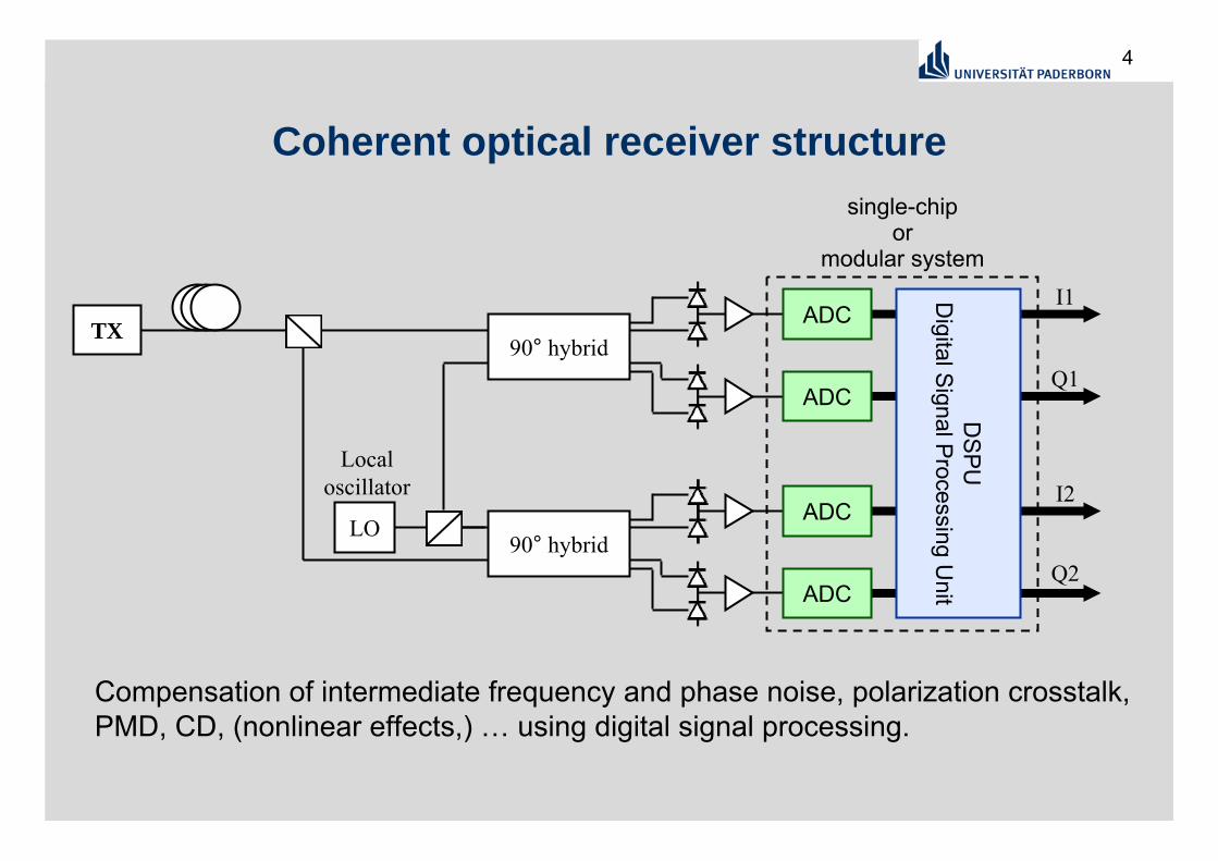
Coherent optical receiver structure
Compensation of intermediate frequency and phase noise, polarization crosstalk, PMD, CD, (nonlinear effects,) … using digital signal processing.
LO
ADC
ADC
ADC
ADC
DSPU
Digital Signal Processing U
nit
Localoscillator
90° hybrid
90° hybrid
I1
Q1
I2
Q2
TX
single-chipor
modular system

R. Noé 5
Internal structure of the DSPU
……… …
1:m demux
ADC
1:m demux
ADC
1:m demux
ADC
1:m demux
ADC
……… …
I1 Q1 I2 Q2
T-spaced sampling:fIN = 1/TS
T/2-spaced sampling:fIN = 2/TS
fDIV = fIN/m
feedback path
m:1 mux
m:1 mux
m:1 mux
m:1 mux fOUT = 1/TS
Algorithmsmust be compatible to
the receiver structure!

R. Noé 6
Demultiplexing and parallelization allows to use standard logic elements with relaxed clock speed requirements.
Delay robustness of control algorithms for all the cases when feedback loops cannot be avoided at all.
Efficient hardware is required to enable a high degree of parallelization with moderate area and power consumption.
Real-time constraints for receiver DSP algorithms
R. Noé 7
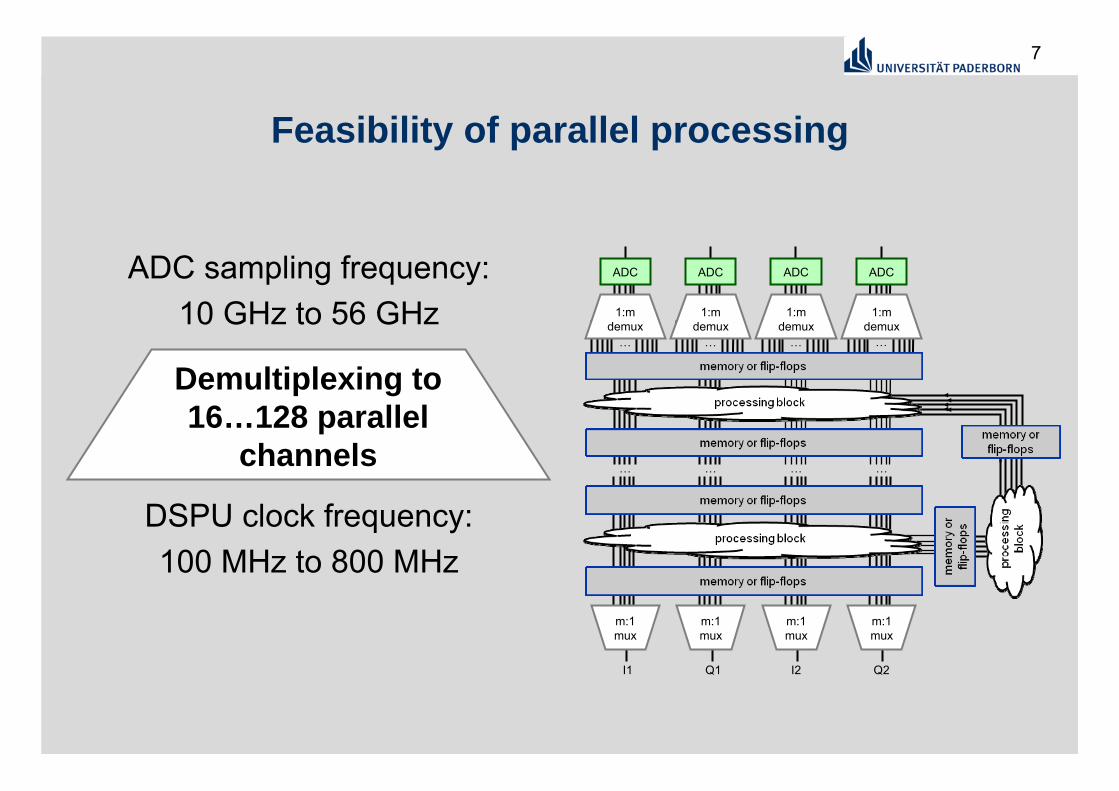
Feasibility of parallel processing
ADC sampling frequency: 10 GHz to 56 GHz
DSPU clock frequency:100 MHz to 800 MHz
Demultiplexing to16…128 parallel
channels……… …
1:m demux
ADC
1:m demux
ADC
1:m demux
ADC
1:m demux
ADC
……… …
I1 Q1 I2 Q2
m:1 mux
m:1 mux
m:1 mux
m:1 mux

R. Noé 8
++++
Comparison of FIR and IIR filters
xk T T
+ yk
α0 α1 α2
xk-1 xk-2 yk
TT
+
xk
β1β2
yk-1yk-2
++++
serial
parallel
data not instantly available

R. Noé 9
Real-time constraint: Hardware efficiency
Computationally complex algorithms increase the required chip area, power consumption and cost.
• Signal transformations, example: FFT/ IFFTWays to increase hardware efficiency:
Convolution MultiplicationFFT/IFFT• Use of look-up tables
• Optimization of the required precision

R. Noé 10
Real-time constraint: Tolerance against feedback delays
Digital signal processing for coherent optical receivers requires massive
• parallel processing,• pipelining.
……… …
1:m demux
ADC
1:m demux
ADC
1:m demux
ADC
1:m demux
ADC
……… …
I1 Q1 I2 Q2
m:1 mux
m:1 mux
m:1 mux
m:1 mux

R. Noé 11
ψk
Decision-directed carrier recovery
decision circuit +
-
exp{-j( )}
arg( )
arg( )
W(z)
Yk
^FF
Xk^
filter function
1ˆ −− kje ψ
…
W(z)
exp{-j( )}FF
Decision circuit +
-arg( )
arg( )
FF
FF
FFFFDecision circuit +
-arg( )
arg( )
FF
FF
FFFFDecision circuit +
-arg( )
arg( )
FF
FF
FFFFdecision circuit +
-arg( )
arg( )
FF
FF
FFFF
FF
FF
Yk
Yk-m+1
…
Xk-2m^
Xk-3m+1^
ψk-4m^mkje 5ˆ −− ψ
Feedback delay of 1 symbol
Linewidth tolerance is significantly reduced!

R. Noé 12
Feedforward carrier recovery
(·)4 ∑2NCR+1
arg(−(·)) (·)/4Yk kϕ̂
Viterbi & Viterbi Algorithm [1]:
Barycenter-Algorithm [2]:(·)modπ
2arg(·)Yk kϕ̂
-1.5 -1 -0.5 0 0.5 1 1.5-1.5
-1
-0.5
0
0.5
1
1.5
+2. Polarisation
2nd Polarization
[1] R. Noé, IEEE J. Lightwave Technology, Vol. 23, No. 2, Feb. 2005, pp. 802-808[2] S. Hoffmann et al., IEEE Photon. Technol. Lett., Vol. 21, No. 3, Feb. 2009, pp. 137-139
kϕ

R. Noé 13
Barycenter algorithm
(·)modπ2arg(·)Yk kϕ̂
Inherent weighting due to multiple use
of inputs
Re
Im
Each filter cell averages pairwise along shortest path.

R. Noé 14
Digital synchronous QPSK receiver scheme
X(i)
LPF
(⋅)4 (X(i))4
(X(i−1))4
(X(i−2))4
(X(i−2N))4
Y(i)(1/4)arg(− (⋅))
X(i−N) arg(⋅)
ϕ(i)
ψ(i) nr(i)
nr(i−1)
nj(i)
no(i)
o1(i), o2(i)ϕ(i−1)
Im X
Re Xdemulti-plexed output data bits o1, o2
ETX
ELO
l21l12
l11
l22LO
TXfiber
A/D
and
1:MDEMUX
Mod. 1
Mod. 2
Mod. M
Frequency quadrupling
Lowpass filtering
Signal phase
Carrier phase angle
Quadrant phase number (0, 1, 2, 3)
Differential decoding of quadrant phase number, taking carrier phase jumps into account
Module (i mod M)All signals it needs from neighbor modules are already available.
X ~ ETX ELO*
Differential encoding of data quadrant number nd in TX
Functionally identical with analog scheme

R. Noé 15
d1, Re c, o1 d2, Im c, o2 nd, nc, no
1 1 0-1 1 1-1 -1 21 -1 3
Detection and correction of quadrant phase jump
physical course
nj(i0)⋅π/2
π/4
−π/4
0i0i0−1
chosen course
ϕ
i0
1
2
3nj
no(i) = nd(i−N)
nr(i)
i0i0−1 i
nc(i−N)
0
1
2
3
nr(i)−nr(i−1)0
1
2
3
nj(i)
Data bits d1, d2 ⇔ quadrant number nd
Differential encoding of quadrant number in transmitter:Differential decoding of quadrant number in receiver, taking phase jumps into account !
( ) ( ) ( )( ) 4mod1−+= ininin cdc

R. Noé 16
Electronic polarization controlX1(i)
X2(i)
data recovery 1
data recovery 2
M
ϕ(i)
nj(i)
ϕ(i−1)
Z(i)
(X1(i))4
(X2(i))4
Z(i−1) Z(i−2) Z(i−2N)
LPF (1/4)arg(− (⋅))Y(i)
R1(i)
R2(i)
ϕ(l)cos(⋅), sin(⋅) e
−jϕ(l)
X1(l−N), X2(l−N)
nr,1(l), nr,2(l)
Q(l) M(l)
Xp(i)
(⋅)4 (Xp(i))4
Xp(i−N) arg(⋅)ϕ(i)
ψp(i)
nj(i)no,p(i)
op1(i), op2(i)
nr,p(i)
nr,p(i−1)
MQM 1: −=
Q
1Q →( ) += ANAN
( ) ( ) ( ) ( ) ( )+− ⋅⋅−⋅= ieNii ij rXQ ϕ21
( )( )MQ11M −+= g:
be a perfect estimate of MJ
⇒A be a data vector ⇒
results in well sufficient accuracy of matrix elements and control time constant on the order of ≤ 103 cycles. At 10 Gbaud control time constants down to ≤ 100 ns are possible.
( ) 11 −− == JMMJ( )( ) 11 −− −−= Q11Q ( )Q11 −+≈
310−≥g

R. Noé 17
Carrier & data recovery
CorrelationMatrix-update
Decision-directed polarization control
⎥⎦
⎤⎢⎣
⎡
yk
xk
YY
,
,⎥⎦
⎤⎢⎣
⎡
yk
xk
ZZ
,
,
⎥⎦
⎤⎢⎣
⎡
yk
xk
cc
,
,
ˆˆ
-1.5 -1 -0.5 0 0.5 1 1.5
-1.5
-1
-0.5
0
0.5
1
1.5
Mk
-1.5 -1 -0.5 0 0.5 1 1.5
-1.5
-1
-0.5
0
0.5
1
1.5
Qk
kϕ̂
+−
⎥⎥⎦
⎤
⎢⎢⎣
⎡
⎥⎥⎦
⎤
⎢⎢⎣
⎡=
yk
xkj
yk
xkk c
ce
YY
k
,
,ˆ
,
,ˆˆϕQ
R. Noé, IEEE Photon. Technol. Lett., Vol. 17, No. 4, April 2005, pp. 887-889
Control target is to force the correlation to the unity matrix.
( ) kkkk g MQ1MM −+=+ :1
Phase offsetsare compensated!

R. Noé 18
DSP components for real-time synchronous QPSK transmission
ADCDE
MUX
DSPUADC
DEMU
X
ADC
DEMU
X
ADC
DEMU
XADC
DEMUX
DSPUADC
DEMU
X
ADC DEMU
X
ADC
DEMUX
Single-chip system Multi-chip system
☺ Highest integration → small footprint
☺ Simple interfacingCommon technology for ADCs and DSPU→ suboptimal performance
☺ Optimum performance☺ Possibility to use commercial ADCs
Complex interfaceIncreased footprint
R. Noé 19
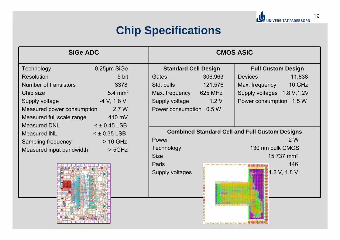
SiGe ADC CMOS ASIC
Technology 0.25µm SiGeResolution 5 bitNumber of transistors 3378Chip size 5.4 mm2
Supply voltage -4 V, 1.8 VMeasured power consumption 2.7 WMeasured full scale range 410 mVMeasured DNL < ± 0.45 LSBMeasured INL < ± 0.35 LSBSampling frequency > 10 GHzMeasured input bandwidth > 5GHz
Standard Cell DesignGates 306,963Std. cells 121,576Max. frequency 625 MHzSupply voltage 1.2 VPower consumption 0.5 W
Full Custom DesignDevices 11,838Max. frequency 10 GHzSupply voltages 1.8 V,1.2VPower consumption 1.5 W
Combined Standard Cell and Full Custom DesignsPower 2 WTechnology 130 nm bulk CMOSSize 15.737 mm2
Pads 146Supply voltages 1.2 V, 1.8 V
Chip Specifications

R. Noé 20
5-bit 10-GS/s analog-to-digital converter
O. Adamczyk et al., Electron. Lett., Vol. 44, No. 15, July 2008, pp. 895-896
technology 0.25 μm SiGe:C BiCMOS
resolution 5 bit
number of transistors 3378
chip size 5.4 mm2
supply voltages -4 V+1.8 V
measured power consumption 2.7 W
measured full scale range (VFSR) 410 mV
measured DNL < ± 0.45 LSB
measured INL < ± 0.35 LSB
sampling frequency > 10 GHz
measured input bandwidth > 5 GHz (10 GSymbol/s)
measured SNR up to 30 dB

R. Noé 21
Digital signal processing unit
Full-custom Standard-cell ASIC
Complexity [transistors] 11,838 1,216,000 1,227,838
Area [mm²] 5.952 5.34 15.737
Frequency [MHz] 5,000 half-rate 625 5,000 half-rate
Power Supply [V] 1.8 1.2 1.8, 1.2

R. Noé 22
Digital signal processing unit
Full-custom Standard-cell ASIC
Complexity [transistors] 11,838 1,216,000 1,227,838
Area [mm²] 5.952 5.34 15.737
Frequency [MHz] 5,000 half-rate 625 5,000 half-rate
Power Supply [V] 1.8 1.2 1.8, 1.2

R. Noé 23
Components
5-bit 10 Gsample/s flash A/D converter chip Size: 2.1 mm×2.55 mm 0.25µm SiGe
CMOS ASIC4.1 mm×4.1 mm 130 nm bulk CMOS
Co-packaged module Ceramic substrate 8.5 cm×6.0 cm
R. Noé 24
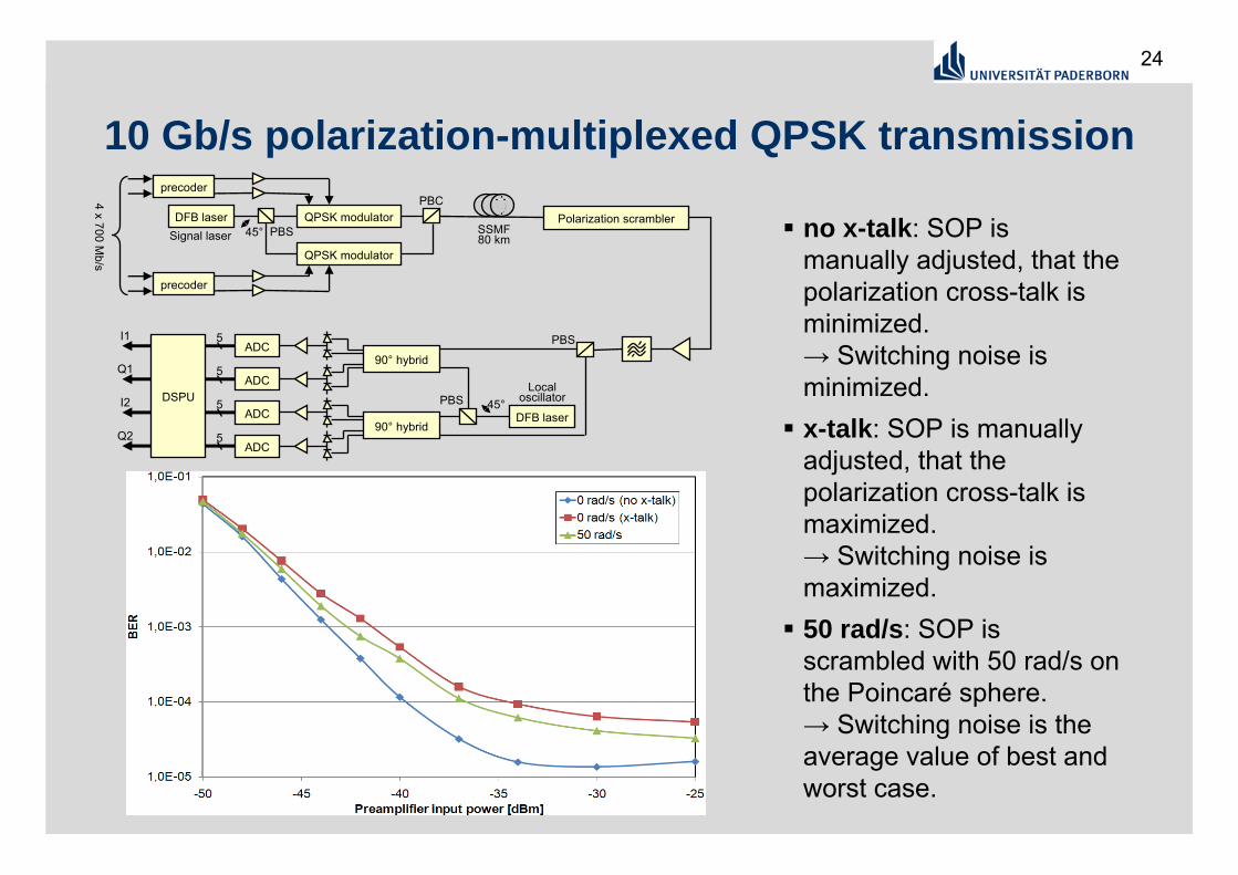
10 Gb/s polarization-multiplexed QPSK transmission
no x-talk: SOP is manually adjusted, that the polarization cross-talk is minimized.→ Switching noise is minimized.x-talk: SOP is manually adjusted, that the polarization cross-talk is maximized.→ Switching noise is maximized.50 rad/s: SOP is scrambled with 50 rad/s on the Poincaré sphere.→ Switching noise is the average value of best and worst case.
DFB laser QPSK modulator
QPSK modulator
4x 700 M
b/s
PBS
PBC
Signal laser 45° SSMF80 km
Polarization scrambler
precoder
precoder
DFB laser
ADC
ADC
ADC
ADC5
5
5
5
DSPU
PBS
PBSLocal
oscillator45°
90° hybrid
90° hybrid
I1
Q1
I2
Q2

R. Noé 25
25
Experimental transmission setup
4x 700 M
b/s
I1
Q1
I2
Q2
DFB laser QPSK modulator
QPSK modulator
PBS
PBC
Signal laser 45° SSMF80 km
12 motorized quarterwave plates
HWP
precoder
precoder
motorizedhalf-wave plate
(bulk optic)
DFB laser
ADC
ADC
ADC
ADC5
5
5
5
Xilinx Virtex 4 FPGA
PBS
PBSLocal
oscillator 45°
90° hybrid
90° hybrid
polarization scrambler
PDLvariable
PDL element(0…6 dB)
VOA
CeLight Israel
Photline
Poincaré sphere traces measured with polarized signal:

R. Noé 26
Measurement results – fast polarization changes & receiver sensitivity penalty
0 krad/s20 krad/s40 krad/s
c=0.75μsc=3.00 μs+
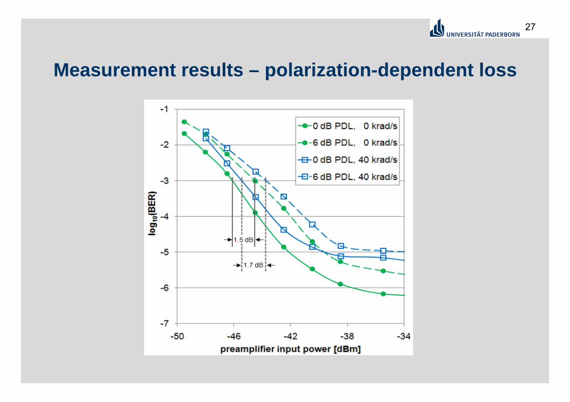
R. Noé 27
Measurement results – polarization-dependent loss

R. Noé 28
Generation of fast endless polarization changes by mechanical halfwave plate, inserted between fiberoptic quarterwave plates

R. Noé 29
Conclusion
General real-time requirements for the DSPU: Parallelization Delay tolerance Hardware EfficiencyAngle-based phase recovery concept (barycenter): simple, linewidth-tolerantPolarization diversity with automatic polarization demultiplexRealtime coherent receiver implementation: SiGe ADC, CMOS DSPUTest results: 10 Gb/s, 40 krad/s

R. Noé 30
Acknowledgement
European CommissionFP6 contract 004631http://ont.upb.de/synQPSK
synQPSKUniv. Paderborn, GermanyCeLight IsraelPhotline, FranceIPAG, GermanyUniv. Duisburg-Essen, Germany
Thank you for your attention!