smart pavement monitoring system - home | … · smart pavement monitoring system ... structural...
TRANSCRIPT

Research, Development, and TechnologyTurner-Fairbank Highway Research Center6300 Georgetown PikeMcLean, VA 22101-2296
Smart Pavement Monitoring System
Publication no. FHWa-HRt-12-072 MaY 2013

FOREWORD
This report documents the development of a novel self-powered sensor system for continuous structural health monitoring of new/reconstruction or resurfacing of asphalt and concrete pavements. The system consists of a wireless integrated circuit sensor that consumes less than 1 microwatt of power and interfaces directly with and draws its operational power from a piezoelectric transducer. Each sensor node is self-powered and capable of continuously monitoring and storing the dynamic strain levels in pavement structure. The data from all the sensors are periodically uploaded wirelessly through radio frequency (RF) transmission using a RF reader either manually operated or mounted on a moving vehicle. The integrated wireless sensor can provide many benefits to highway agencies by helping facilitate more effective pavement maintenance and rehabilitation/preservation decision making by detecting possible damage, monitoring mechanical load history, and predicting the fatigue life of the monitored pavements.
Jorge E. Pagán-Ortiz Director, Office of Infrastructure Research and Development
Notice This document is disseminated under the sponsorship of the U.S. Department of Transportation in the interest of information exchange. The U.S. Government assumes no liability for the use of the information contained in this document. This report does not constitute a standard, specification, or regulation.
The U.S. Government does not endorse products or manufacturers. Trademarks or manufacturers’ names appear in this report only because they are considered essential to the objective of the document.
Quality Assurance Statement The Federal Highway Administration (FHWA) provides high-quality information to serve Government, industry, and the public in a manner that promotes public understanding. Standards and policies are used to ensure and maximize the quality, objectivity, utility, and integrity of its information. FHWA periodically reviews quality issues and adjusts its programs and processes to ensure continuous quality improvement.

TECHNICAL REPORT DOCUMENTATION PAGE 1. Report No. FHWA-HRT-12-072
2. Government Accession No. 3. Recipient’s Catalog No.
4. Title and Subtitle Smart Pavement Monitoring System
5. Report Date May 2013 6. Performing Organization Code
7. Author(s) Nizar Lajnef, Karim Chatti, Shantanu Chakrabartty, Mohamed Rhimi, and Pikul Sarkar
8. Performing Organization Report No.
9. Performing Organization Name and Address Michigan State University 426 Auditorium Road East Lansing, MI 48824
10. Work Unit No. (TRAIS)
11. Contract or Grant No. DTFH61-08-C-00015
12. Sponsoring Agency Name and Address Federal Highway Administration Office of Acquisition Management 1200 New Jersey Avenue SE Washington, DC 20590
13. Type of Report and Period Covered Final Report, September 2008–July 2012 14. Sponsoring Agency Code
15. Supplementary Notes The Contracting Officer’s Representative (COR) was Fred Faridazar, HRDI-20. 16. Abstract This report describes the efforts undertaken to develop a novel self-powered strain sensor for continuous structural health monitoring of pavement systems under the Federal Highway Administration. Efforts focused on designing and testing a sensing system that consists of a novel self-powered wireless sensor capable of detecting damage and loading history for pavement structures. The developed system is based on the integration of a piezoelectric transducer with an array of ultra-low power floating gate computational circuits. A miniaturized sensor was developed and tested. The sensor is capable of continuous battery-less monitoring of strain events integrated over the occurrence duration time. The work conducted under this project resulted in the following: • The development of a sensor that has the following attributes: (1) Self-powered, continuous, and autonomous
sensing; (2) autonomous computation and non-volatile storage of sensing variables; (3) small size such that it can be installed using existing installation procedures that are accepted by State highway agencies and will not constitute a major disruption to current practices; (4) wireless communication to eliminate the need for embedding wires in the pavement structure and the use of fixed data acquisition systems on the side of the road; (5) robustness to withstand harsh loading and environmental conditions during initial construction and throughout the life of the pavement; and (6) the ability of integration in large-scale sensor networks.
• The manufacturing of the sensor electronics and the characterization of their basic functionalities in a laboratory setting.
• The design and characterization of the self-powering scheme based on piezoelectric transduction. • The design and testing of a robust packaging system to withstand loading and environmental conditions for
field implementation. • The development of a sensor-specific data interpretation algorithm for predicting remaining fatigue life of a
pavement structure using cumulative limited compressed strain data stored in the sensor memory. 17. Key Words Pavement management, Structural health monitoring, Smart self-powered sensors, Remaining fatigue life prediction
18. Distribution Statement No restrictions. This document is available through the National Technical Information Service, Springfield, VA 22161.
19. Security Classification (of this report) Unclassified
20.Security Classification (of this page) Unclassified
21. No. of Pages 146
22. Price N/A
Form DOT F 1700.7 (8-72) Reproduction of completed page authorized

ii

iii
TABLE OF CONTENTS
CHAPTER 1. INTRODUCTION .................................................................................................1 1.1 BACKGROUND ............................................................................................................... 1 1.2 PROJECT SCOPE............................................................................................................ 2 1.3 PROJECT OBJECTIVES................................................................................................ 2 1.4 REPORT STRUCTURE .................................................................................................. 3
CHAPTER 2. SMART SENSING SYSTEM DEVELOPMENT ..............................................5 2.1 SELF-POWERED SENSOR DESIGN ........................................................................... 5 2.2 PRELIMINARY LABORATORY EVALUATION ...................................................... 9 2.3 SENSOR ELECTRONICS REFINEMENT ................................................................ 14
2.3.1 Voltage Regulators................................................................................................... 17 2.3.2 Additional Changes .................................................................................................. 22 2.3.3 Linear FG Sensor ..................................................................................................... 23 2.3.4 Over-Voltage Protection Circuit .............................................................................. 25
2.4 CONCLUSION ............................................................................................................... 26
CHAPTER 3. DEVELOPMENT OF WIRELESS COMMUNICATION AND DATA UPLOAD PROTOCOL ...............................................................................................................27
3.1 SYSTEM DESIGN .......................................................................................................... 27 3.2 CIRCUIT IMPLEMENTATION .................................................................................. 28
3.2.1 Envelope Recovery Circuit ...................................................................................... 30 3.2.2 ADC ......................................................................................................................... 33 3.2.3 Voltage Multiplier .................................................................................................... 34 3.2.4 Demodulator and Backscatter Modulator ................................................................ 35 3.2.5 High-Voltage Generator........................................................................................... 36 3.2.6 DBM ........................................................................................................................ 37
3.3 TESTING PROCEDURES AND MEASURED RESULTS ....................................... 38 3.3.1 Testing RF Signal Propagation through Concrete and Asphalt ............................... 42
3.4 CHALLENGES AND IMPLEMENTED SOLUTIONS ............................................. 45 3.4.1 RF Matching Network ............................................................................................. 45 3.4.2 RF Matching Network—Voltage-Boosting Method ............................................... 47
3.5 CONCLUSION ............................................................................................................... 51
CHAPTER 4. LABORATORY MECHANICAL TESTING OF THE PIEZOELECTRIC TRANSDUCER .........................................................................................53
4.1 PIEZOELECTRIC TRANSDUCER DESIGN AND TESTING ................................ 53 4.2 PIEZOELECTRIC TRANSDUCER CALIBRATION ............................................... 55 4.3 LABORATORY TESTING OF EMBEDDED SYSTEM ........................................... 61
4.3.1 AC Beam Testing ..................................................................................................... 62 4.3.2 Concrete Beam Testing ............................................................................................ 64
4.4 CONCLUSION ............................................................................................................... 68
CHAPTER 5. DESIGN OF ROBUST PACKAGING SYSTEM AND INITIAL FIELD TRIALS ...........................................................................................................................69
5.1 CURRENT STATE OF THE PARCTICE FOR STRAIN GAUGE INSTALLATION TECHNIQUES ...................................................................................... 69

iv
5.2 SYSTEM DESIGN .......................................................................................................... 74 5.2.1 Thermal Insulation ................................................................................................... 74 5.2.2 Mechanical Protection ............................................................................................. 75 5.2.3 Package Design for Implementation in HMA ......................................................... 77 5.2.4 Laboratory Testing and Results ............................................................................... 81
5.3 PRELIMINARY LARGE-SCALE TESTING ............................................................. 83 5.4 CONCLUSION ............................................................................................................... 93
CHAPTER 6. LABORATORY FATIGUE TESTING AND DEVELOPMENT OF SENSOR-SPECIFIC DAMAGE PROGNOSIS ALGORITHMS ....................................95
6.1 DATA INTERPRETATION ALGORITHMS ............................................................. 95 6.2 ALGORITHM EVALUATION USING CONCRETE BEAM FLEXURAL BENDING FATIGUE TESTS ............................................................................................. 99 6.3 ESTIMATION OF REMAINING LIFE—PRELIMINARY RESULTS ................ 104
6.3.1 Mechanistic-Empirical Approach .......................................................................... 105 6.3.2 Probabilistic Approach........................................................................................... 106
6.4 DATA IMPUTATION—MISSING FULL-FIELD DATA GENERATION........... 109 6.5 CONCLUSION ............................................................................................................. 115
CHAPTER 7. CONCLUSION ..................................................................................................117 7.1 RECOMMENDATIONS FOR FUTURE RESEARCH AND DEVELOPMENT.. 119
APPENDIX A. DEVELOPMENT AND LABORATORY TESTING OF A PASSIVE TEMPERATURE GAUGE .....................................................................................121
A.1 SENSOR DESIGN AND TESTING ........................................................................... 121
APPENDIX B. INTEGRATION AND LABORATORY TESTING OF WIRELESS PROTOCOL WITH OTHER EXISTING INSTRUMENTATION .....................................123
B.1 TESTING ...................................................................................................................... 123
APPENDIX C. DATASHEET AND CALIBRATION CERTIFICATE FOR USED COD GAUGE .................................................................................................................127
APPENDIX D. DATASHEET FOR USED LVDTS ...............................................................129
REFERENCES ...........................................................................................................................131

v
LIST OF FIGURES
Figure 1. Illustration. Array of self-powered sensors capable of monitoring cumulative strain history of the host pavement structure .............................................................................................2 Figure 2. Illustration. Complete circuit implementation of self-powered event counter .................5 Figure 3. Illustration. IIHEI process in a PMOS FG transistor .......................................................6 Figure 4. Illustration. IIHEI using an energy band diagram ............................................................6 Figure 5. Illustration. Concept of piezoelectricity-driven IIHEI .....................................................7 Figure 6. Illustration. Electrical model of an analog FG memory cell ............................................7 Figure 7. Equation. IIHEI current ....................................................................................................8 Figure 8. Equation. Source current ..................................................................................................8 Figure 9. Equation. FG voltage ........................................................................................................8 Figure 10. Equation. Injection current as a function of the FG voltage...........................................8 Figure 11. Equation. Differential equation for the source voltage ..................................................9 Figure 12. Equation. System variables ............................................................................................9 Figure 13. Equation. Source voltage as a function of the cumulative duration of the injection process, t ..........................................................................................................................................9 Figure 14. Photo. Sensor prototype manufactured on a DIP40 packaging system ..........................9 Figure 15. Photo. Prototype mounted on a testing board and connected to a computer using a parallel port for data upload ..............................................................................................10 Figure 16. Graph. Theoretical and measured results for source voltage response ........................10 Figure 17. Equation. Source voltage for short-term monitoring ....................................................10 Figure 18. Equation. Source voltage for long-term monitoring .....................................................11 Figure 19. Equation. Change in source voltage .............................................................................11 Figure 20. Graph. Injector response measured at various source currents ....................................12 Figure 21. Graph. Injector response measured by using eight prototypes fabricated in different runs ..................................................................................................................................12 Figure 22. Graph. Injector response measured under different temperature conditions ................13 Figure 23. Illustration. Sensor connection package .......................................................................14 Figure 24. Photo. Sensor interface board .......................................................................................14 Figure 25. Illustration. System architecture of the entire sensor ...................................................17 Figure 26. Illustration. Conventional OPAMP-based regulator ....................................................18 Figure 27. Illustration. Diodic current conveyer regulator ............................................................18 Figure 28. Graph. Simulated response for the OPAMP-based regulator .......................................19 Figure 29. Graph. Simulated response for the diodic regulator .....................................................19 Figure 30. Illustration. Measured results from an OPAMP-based LDO showing potential stability problems ...........................................................................................................................20 Figure 31. Graph. Measured responses for a fabricated diodic regulator ......................................21 Figure 32. Graph. Measured responses for a fabricated diodic regulator with a longer diodic chain ....................................................................................................................................21 Figure 33. Illustration. Piezo-sensor module .................................................................................23 Figure 34. Illustration. RF interrogation module on separate silicon substrates/ICs .....................23 Figure 35. Illustration. Ultra-linear FG injector circuit .................................................................24 Figure 36. Graph. Measured response of the linear injector circuit showing a dynamic range greater than 4 V and resolution greater than 13 bits ............................................................25 Figure 37. Graph. Measured resolution over a dynamic range of 4 V output ...............................25

vi
Figure 38. Graph. Measured response from over-voltage protection circuit showing the output clamped to 9 V ....................................................................................................................26 Figure 39. Illustration. Principle of HF RFID used in the sensing system ....................................27 Figure 40. Illustration. Equivalent circuit model for the RFID system and the load modulation scheme for wireless communication ...........................................................................28 Figure 41. Equation. Input voltage ................................................................................................28 Figure 42. Illustration. System-level architecture of the wireless communication system for the sensor ..................................................................................................................................29 Figure 43. Illustration. Architecture of the sensor .........................................................................29 Figure 44. Photo. Micrograph of the sensor prototyped in a 0.02-mil (0.5-µm ) CMOS process............................................................................................................................................30 Figure 45. Illustration. Envelope recovery module .......................................................................30 Figure 46. Illustration. Output of the envelope recovery module using hysteretic and non-hysteretic comparators when a noisy RF signal is applied .....................................................31 Figure 47. Illustration. Hysteretic comparator used in the improved envelope recovery circuit .............................................................................................................................................31 Figure 48. Graph. Output of the envelope recovery module using hysteretic and non-hysteretic comparators when a valid ASK modulated RF signal is applied ...........................32 Figure 49. Illustration. Measured output of the envelope recovery module using hysteretic and non-hysteretic comparators when a valid ASK modulated RF signal is applied ....................33 Figure 50. Illustration. Functional architecture of the single-slope ADC......................................33 Figure 51. Equation. Residential value in the counter ...................................................................34 Figure 52. Graph. Digital output stream produced by the ADC when the input voltage is varied ..........................................................................................................................................34 Figure 53. Illustration. Structure of the Dickson voltage multiplier ..............................................35 Figure 54. Equation. Output voltage ..............................................................................................35 Figure 55. Illustration. Function blocks of the modulator and demodulator .................................36 Figure 56. Illustration. Charge pump used for implementing the high-voltage generator ............36 Figure 57. Illustration. Timing diagram of the non-overlapping clock generator .........................37 Figure 58. Graph. Sample results from fabricated prototype.........................................................37 Figure 59. Illustration. State machine implemented by DBM .......................................................38 Figure 60. Photo. Manufactured external reader and internal interface board ..............................39 Figure 61. Photo. Second prototype antenna adapted to the H-shaped gauge ...............................39 Figure 62. Illustration. Measured results for ASK modulation .....................................................40 Figure 63. Illustration. Close-up view of measured results for ASK modulation .........................40 Figure 64. Illustration. Measured results showing the sensor entering an injection state .............41 Figure 65. Illustration. Measured results showing the sensor entering a tunneling state ..............41 Figure 66. Illustration. Measured results showing the sensor data received by the reader when it sends an acquire command ...............................................................................................42 Figure 67. Illustration. Measured results showing multi-channel sensor data received by the reader when the sensor is in a continuous sampling state ..............................................................42 Figure 68. Photo. Sensor placed under a concrete specimen .........................................................43 Figure 69. Photo. Receiver placed on top of the concrete specimen .............................................43 Figure 70. Photo. Concrete specimen placed between a reader and receiver ................................43 Figure 71. Photo. Test setup with an asphalt concrete (AC) specimen introduced between the reader and the receiver ...............................................................................................43
vii
Figure 72. Photo. Oscilloscope showing the voltage measured at the receiver .............................44 Figure 73. Illustration. Communication signals transmitted through concrete ..............................44 Figure 74. Illustration. Communication signals transmitted through asphalt ................................44 Figure 75. Flowchart. Design flow to optimize the matching network that can maximize the powering and reading distance between the sensor and the reader .........................46 Figure 76. Graph. Simulation results showing the power received at the sensor when the sensor-reader distance is varied ...............................................................................................47 Figure 77. Graph. Simulation results showing the voltage induced at the sensor when the sensor-reader distance is varied .....................................................................................................47 Figure 78. Photo. Experimental setup used to validate the proposed reactive voltage-boosting method ................................................................................................................48 Figure 79. Illustration. Equivalent circuit model for the setup ......................................................49 Figure 80. Graph. Non-linear resistive model for the voltage multiplier on the sensor IC ...........49 Figure 81. Graph. Comparison of the voltage generated by an 18-stage voltage multiplier for the new and the previously used matching network ................................................................50 Figure 82. Graph. Comparison of the voltage generated by a 12-stage voltage multiplier for the new and previously used matching network ......................................................................50 Figure 83. Photo. Experimental setup for the indirect tensile test .................................................54 Figure 84. Photo. Command unit for the indirect tensile test setup ...............................................54 Figure 85. Photo. Piezoelectric disk transducer attached to the tested asphalt specimen ..............54 Figure 86. Graph. Correlation between measured strains and voltage output of the transducer at varying temperatures ................................................................................................55 Figure 87. Illustration. Piezoelectric strain scavenger ................................................................55 Figure 88. Equation. Varitional indicator ......................................................................................56 Figure 89. Equation. Kinetic energy ..............................................................................................56 Figure 90. Equation. External work ...............................................................................................56 Figure 91. Equation. Potential energy............................................................................................56 Figure 92. Equation. Variational indicator ....................................................................................57 Figure 93. Equation. Longitudinal displacement ...........................................................................57 Figure 94. Equation. Electric field .................................................................................................57 Figure 95. Equation. Piezoelectric constitutive equation ...............................................................57 Figure 96. Equation. Stiffness ........................................................................................................57 Figure 97. Equation. Applied load induced by strain ....................................................................57 Figure 98. Equation. Electromechanical coupling and capacitance matrices ................................58 Figure 99. Graph. Voltage transfer function of PVDF film and PZT piezo under 400 microstrain loading across 10 megaohm load resistance ........................................................58 Figure 100. Graph. Output voltage amplitude of PVDF film and PZT piezo under 400 microstrain versus load resistance ..........................................................................................59 Figure 101. Photo. PVDF piezo film bounded to Plexiglas® beam ...............................................59 Figure 102. Photo. PVDF embedded in epoxy and bounded to Plexiglas® beam .........................60 Figure 103. Photo. PVDF piezo film embedded in epoxy and bounded to concrete .....................60 Figure 104. Photo. Bending test setup to check the activation strain loss from a configuration to another .................................................................................................................60 Figure 105. Photo. Setup of sensor calibration and fatigue tests ...................................................61 Figure 106. Photo. Slab compactor ................................................................................................62 Figure 107. Photo. Compacted slab with embedded transducers ..................................................62

viii
Figure 108. Photo. Cut asphalt specimen with embedded piezoelectric generator .......................63 Figure 109. Graph. Sample of voltage response of PZT with time under applied sinusoidal strain ...............................................................................................................................................63 Figure 110. Photo. Piezoelectric transducer embedded in concrete ..............................................64 Figure 111. Photo. Piezoelectric transducer covered with a layer of rubber .................................64 Figure 112. Photo. Concrete specimen with embedded piezoelectric generator ...........................65 Figure 113. Photo. Concrete specimen loaded in a temperature-controlled environment .............65 Figure 114. Graph. Sample voltage response of embedded PZT at 14 °F (-10 °C) under applied 177 and 441 microstrain load ............................................................................................66 Figure 115. Graph. Sample voltage response of embedded PZT under 278 microstrain at 32 and 86 °F (0 and 30 °C) ............................................................................................................66 Figure 116. Graph. Correlation between measured strains and voltage output of the transducer at varying temperatures ................................................................................................67 Figure 117. Graph. Effect of temperature on the output voltage at different levels of fluctuating strains ...........................................................................................................................68 Figure 118. Photo. Example of commercially available asphalt strain gauge ...............................69 Figure 119. Photo. Second example of commercially available asphalt strain gauge ...................69 Figure 120. Photo. Marking the proposed locations of the gauges ................................................71 Figure 121. Photo. Placing sand/binder pad and fitting gauges .....................................................71 Figure 122. Photo. Placing screened asphalt on top of gauges and carefully compacting ............71 Figure 123. Photo. Compacting the unscreened asphalt over the gauge arrays .............................72 Figure 124. Photo. Laying instrument wiring and piping in aggregate base .................................72 Figure 125. Photo. Cutting grooves in cement-treated base for instrument leads .........................72 Figure 126. Photo. Collecting a concrete strain gauge using steel frames ....................................73 Figure 127. Illustration. Cross section of commercialized strain gauges ......................................73 Figure 128. Photo. Thermocouple covered with a layer of polyurethane foam ............................74 Figure 129. Graph. Measured output from protected and unprotected thermocouples .................75 Figure 130. Photo. Testing of the selected protective materials under compaction condition ......76 Figure 131. Photo. Material prototype placed in a compactor .......................................................76 Figure 132. Photo. Compacted asphalt material ............................................................................77 Figure 133. Photo. Material specimen recovered from the asphalt beam after compaction ..........77 Figure 134. Illustration. Finite element model of the H-shaped package ......................................78 Figure 135. Illustration. Simulated stress distributions .................................................................78 Figure 136. Illustration. Simulated nodal deflections ....................................................................78 Figure 137. Photo. Manufacturing process of the used molds .......................................................79 Figure 138. Photo. Molds forming .................................................................................................79 Figure 139. Photo. Finished molds ................................................................................................79 Figure 140. Photo. Piezoelectric transducer embedded in Araldite® GY-6010 epoxy ..................80 Figure 141. Photo. Polyurethane thermal insulator coat deposited on top of the epoxy core .......80 Figure 142. Photo. Tested prototypes of piezoelectric transducer embedded in epoxy and coated with a polyurethane thermal insulator ................................................................................81 Figure 143. Photo. Specimens placed in the compactor ................................................................81 Figure 144. Graph. Measured compaction curves .........................................................................82 Figure 145. Photo. Recovered sample 1 after compaction ............................................................82 Figure 146. Photo. Recovered sample 2 after compaction ............................................................82 Figure 147. Photo. Final version of the prototype with an external resin layer .............................83
ix
Figure 148. Photo. Recovered specimen........................................................................................83 Figure 149. Illustration. Layout of ASGs ......................................................................................84 Figure 150. Graph. Simulated longitudinal strain using Viscoroute .............................................85 Figure 151. Graph. Measured longitudinal strain using thin H-shape and bone shape made of conathane ...................................................................................................................................86 Figure 152. Graph. Measured longitudinal strain using thin H-shape and bone shape made of araldite .......................................................................................................................................86 Figure 153. Graph. Measured longitudinal strain using thick H-shape and bone shape made of conathane .........................................................................................................................86 Figure 154. Graph. Measured longitudinal strain using thick H-shape and bone shape made of araldite..............................................................................................................................87 Figure 155. Graph. Measured longitudinal strain with bone-shaped conathane strain gauges using two different thicknesses ..........................................................................................87 Figure 156. Photo. Prototype installation at TFHRC’s ALF .........................................................88 Figure 157. Photo. Grinding the existing pavement before bonding gauges to the surface ..........88 Figure 158. Photo. Placed sensor prototype...................................................................................88 Figure 159. Photo. Testing the wireless reading functions for the installed prototype .................89 Figure 160. Photo. Different tested types of package prototypes ..................................................89 Figure 161. Photo. Prepared grooves for prototype installation ....................................................89 Figure 162. Photo. Special epoxy used to bond gauges to surface ................................................90 Figure 163. Photo. Installed prototypes .........................................................................................90 Figure 164. Photo. Installation of the prototype packaging system installed during a construction project near Lansing, MI ...........................................................................................91 Figure 165. Photo. Specimen preparation and placement..............................................................91 Figure 166. Photo. Manual compaction of HMA patches .............................................................92 Figure 167. Photo. Installed prototypes ahead of the compactor ...................................................92 Figure 168. Graph. Strain amplitude variation of a concrete beam under cyclic load with constant amplitude .................................................................................................................95 Figure 169. Equation. Strain cumulative density ...........................................................................96 Figure 170. Graph. Cumulative distribution of strain expressed in voltage ..................................96 Figure 171. Graph. Normalized density distribution expressed as normalized voltage ................97 Figure 172. Graph. Relative error of fitting per gate for specimens at different life stages versus number of gates per sensor .................................................................................................97 Figure 173. Equation. Cumulative distribution..............................................................................98 Figure 174. Equation. Cumulative loading time ............................................................................98 Figure 175. Equation. Mean of the cumulative strain ....................................................................98 Figure 176. Equation. Standard deviation......................................................................................98 Figure 177. Equation. Mean of the applied strain amplitude at time t...........................................98 Figure 178. Equation. Standard deviation of the applied strain amplitude at time t......................98 Figure 179. Equation. Mean of the damage coefficient .................................................................98 Figure 180. Equation. Variance of the damage coefficient ...........................................................99 Figure 181. Equation. Reliability index .........................................................................................99 Figure 182. Equation. Probability of failure ..................................................................................99 Figure 183. Graph. Strain distribution histogram at different life stages of the beam at 100 cycles.....................................................................................................................................100

x
Figure 184. Graph. Strain distribution histogram at different life stages of the beam at 25,000 cycles................................................................................................................................100 Figure 185. Graph. Strain distribution histogram at different life stages of the beam at 40,500 cycles................................................................................................................................101 Figure 186. Graph. Fitting the sensor’s output at different life stages of the specimen at 100 cycles.....................................................................................................................................101 Figure 187. Graph. Fitting the sensor’s output at different life stages of the specimen at 25,000 cycles................................................................................................................................102 Figure 188. Graph. Fitting the sensor’s output at different life stages of the specimen at 40,500 cycles................................................................................................................................102 Figure 189. Graph. Probability distribution of the damage coefficient versus the number of cycles of loading ..........................................................................................................................103 Figure 190. Graph. Variance damage coefficient distribution .....................................................103 Figure 191. Graph. Variation of the mean ...................................................................................104 Figure 192. Graph. Probability of failure of one of the samples versus the number of load cycles ....................................................................................................................................104 Figure 193. Graph. Reliability index of one of the samples versus the number of load cycles............................................................................................................................................104 Figure 194. Equation. Linear damage accumulation rule ............................................................105 Figure 195. Equation. Remaining life ..........................................................................................105 Figure 196. Equation. Cumulative distribution function .............................................................106 Figure 197. Graph. Probability density function of the damage index at failure.........................106 Figure 198. Equation. Remaining life CDF .................................................................................107 Figure 199. Equation. Survival probability function of the beam ...............................................107 Figure 200. Equation. Expectation of the survival probability function ......................................107 Figure 201. Equation. Function of the damage index ..................................................................107 Figure 202. Graph. Normalized estimated remaining life versus the normalized specimen’s lifetime using three fitting shape functions ..................................................................................108 Figure 203. Graph. Remaining life probability versus normalized specimen’s lifetime using three fitting shape functions ...............................................................................................108 Figure 204. Graph. Example of data from distributed sensors on a simply supported beam under random loading.........................................................................................................110 Figure 205. Equation. Estimate of X as a function of mu ............................................................110 Figure 206. Equation. System of equations to solve for the case of an OK formulation ............110 Figure 207. Graph. Theoretical and estimated strain probability distributions at 3.74 inches (94.99 mm) using data from groups of three sensors at different locations .............112 Figure 208. Illustration. Example of a class 9 truck used for strain response data generation ....113 Figure 209. Graph. Example of longitudinal strain profile evaluated at the bottom of the HMA layer for a moving load induced by a class 9 truck .....................................................113 Figure 210. Graph. Theoretical and estimated strain probability distributions at a selected transverse location using data from two sensors at different spacing distances ..........................114 Figure 211. Graph. Maximum observed relative error and average relative error from generated data at all field points using known nodes at different spacing distances ...................114 Figure 212. Illustration. Circuit implementation of a temperature-dependent measuring system ..........................................................................................................................................121

xi
Figure 213. Graph. Variations of measured output current (figure 212) with respect to temperature ..................................................................................................................................122 Figure 214. Graph. Variations of measured output voltage with respect to temperature ............122 Figure 215. Photo. Overhead view of Dynamax SM200 moisture gauge ...................................123 Figure 216. Photo. Dynamax SM200 moisture gauge .................................................................124 Figure 217. Graph. Measured output voltage of the moisture cell powered by a 9-V battery ....124 Figure 218. Photo. Testing setup for the moisture cell ................................................................125

xii
LIST OF TABLES
Table 1. Hardware changes that were incorporated in different versions of the sensor IC ...........15 Table 2. Summary of performance metrics of fabricated prototypes ............................................22 Table 3. Piezoelectric sensor properties .........................................................................................56 Table 4. Activation strain at different piezo configurations ..........................................................61 Table 5. Reliability index, probability of failure, and damage coefficient at failure for different specimens ................................................................................................................105 Table 6. Predicted remaining life cycles using M-E calibrated coefficients and using the updated sensor output.............................................................................................................106 Table 7. Estimated remaining life using the different fitting shape function ..............................109

xiii
ABBREVIATIONS
AC Asphalt concrete
ADC Analog-to-digital converter
ALF Accelerated loading facility
ASG Asphalt strain gauge
ASK Amplitude shift key
Caltrans California Department of Transportation
CDF Cumulative density function
CMOS Complementary metal oxide semiconductor
COD Crack-opening displacement
CRC Cyclic redundancy check
DBM Digital base-band module
DIP Dual in-line package
FG Floating gate
FHWA Federal Highway Administration
FPGA Field-programmable gate array
FWD Falling weight deflectometer
HF High frequency
HMA Hot mix asphalt
IC Integrated circuit
IIHEI Impact-ionized hot electron injection
LDO Low dropout voltage
LVDT Linear variable differential transformer
M-E Mechanistic-empirical
MOSFET Metal oxide semiconductor field effect transistor
NMOS N-type metal oxide semiconductor
OK Ordinary Kriging
OPAMP Operational amplifier
PCB Printed circuit board
PCC Portland cement concrete

xiv
PMOS P-type metal oxide semiconductor
PMS Pavement Management System
PSRR Power supply rejection ratio
PVC Polyvinyl chloride
PVDF Polyvinylidene fluoride
PWM Pulse width modulation
PZT Lead zirconate titanate
RF Radio frequency
RFID Radio frequency identification
SHA State highway agency
SiO2 Silicon dioxide
SM Sensor model
SPI Serial peripheral interface
SPS Specific Pavement Studies
TFHRC Turner-Fairbank Highway Research Center
TI Texas Instruments
TSD Traffic speed deflectometer

1
CHAPTER 1. INTRODUCTION
This report describes the efforts undertaken to develop a novel self-powered strain sensor for continuous structural health monitoring of pavement systems, which was conducted under the Federal Highway Administration (FHWA).
1.1 BACKGROUND
State highway agencies (SHAs) typically spend several million dollars per year to monitor the condition of pavement structures as part of developing their Pavement Management System (PMS) databases. Two approaches are typically taken: (1) conducting manual distress surveys or (2) conducting automated condition surveys using specially equipped vehicles. However, these monitoring approaches are reactive instead of proactive in terms of detecting damage since they merely record the distresses that have already appeared. In addition, for thicker pavements, surface cracks may not be indicative of structural damage if they exhibit top-down cracking. The true pavement structural condition and rate of deterioration are needed to plan optimal structural rehabilitation activities and future budget needs. Therefore, with effective pavement preservation activities that intervene early to preserve and extend the life of pavements, surface cracks cannot be used as a reliable indicator of structural condition or health of the pavement structure.
Another approach used to monitor the structural health of the pavement network is deflection testing. The most popular method is using a falling weight deflectometer (FWD), although it has been largely implemented for project-level evaluations as opposed to network-level evaluations mainly because of significant personnel time and costs as well as safety concerns. The latest development of the traffic speed deflectometer (TSD) technology promises to address some of these concerns. However, the current technology is only capable of measuring peak deflection, which is not suitable for predicting remaining fatigue life. Furthermore, TSDs can only be used cost effectively on a periodic basis (e.g., annually or bi-annually). As a result, there is a continuing need for low-cost technologies that facilitate early damage detection and future condition evaluation for pavement network management.
Currently, pavement instrumentation for condition monitoring is done on a localized and short-term basis, mainly for research purposes. The currently used technology does not allow for continuous long-term monitoring because of the limitations caused by the use of batteries (i.e., it is impractical to replace batteries for embedded sensors). Also, the deployment of existing systems on a network level remain unfeasible due to cost, unease of installation and data collection techniques (need for fixed and rather massive data acquisition systems), and low durability (due to required wiring).
Although recently there has been significant research performed on distributed wireless sensors for monitoring industrial process parameters and environmental conditions, all of the commercially viable sensors developed to date require either solar or battery power. It is unlikely that such powering means would be practical for monitoring pavement structures because periodic replacement of batteries or the expense of solar power technology would be cost prohibitive and in some cases impractical (e.g., due to safety on highly trafficked or inaccessible roads). It is believed that energy harvesting could constitute a viable alternative. Energy

2
harvesting (often referred to as “energy scavenging”) is the process of converting ambient energy (i.e., the kinetic energy from structural vibration or mechanical strain) into electrical energy that can be used to power the sensor.
1.2 PROJECT SCOPE
This research focused on designing and testing a sensor system for pavement monitoring. The system consists of a novel self-powered wireless sensor capable of detecting damage and loading history for pavement structures. The developed system is based on the integration of a piezoelectric transducer with an array of ultra-low power floating gate (FG) computational circuits. A miniaturized sensor was developed and tested. It was shown that it is capable of continuous battery-less monitoring of strain events integrated over the occurrence duration time.
Successful development of the proposed strain sensor could dramatically transform the economics of pavement preservation/management and ultimately improve the serviceability of pavements. The developed system consists of a network of low-cost sensors distributed along the pavement. Each sensor node is self-powered and capable of continuously monitoring and storing the dynamic strain levels in the host pavement structure. The strain data are stored onboard the sensor, which consists of the self-powered sensor strip and the small scale electronics. The data from all the sensors are periodically uploaded wirelessly to a central database. The sensor is read through standard radio frequency (RF) transmission using a RF reader that is either manually operated or mounted on a moving vehicle. By directly outfitting service vehicles with low-cost RF transponders, the roads can be frequently monitored to detect changes in structural integrity that may not only foreshadow a future crack/distress manifestation but also allow for more accurate scheduling of preservation actions. It should be noted that only a single RF reader is needed to inspect the sensor network. Given the annual costs of infrastructure inspection, this sensor cost could rapidly pay for itself. Figure 1 shows a schematic of the envisioned system.
Sensors
RF signals
Pavement structure Figure 1. Illustration. Array of self-powered sensors capable of monitoring cumulative
strain history of the host pavement structure.
1.3 PROJECT OBJECTIVES
The objectives of the project are as follows:
• Develop a sensor that has the following attributes: (1) self-powered, continuous, and autonomous sensing; (2) autonomous computation and non-volatile storage of sensing variables; (3) small size such that it can be installed using existing installation procedures

3
that are accepted by SHAs and will not constitute a major disruption to current practices; (4) wireless communication to eliminate the need for embedding wires in the pavement structure and the use of fixed data acquisition systems on the side of the road; (5) robustness to withstand harsh loading and environmental conditions during initial construction and throughout the life of the pavement; and (6) ability of integration in large-scale sensor networks.
• Manufacture sensor electronics and characterize their basic functionalities in a laboratory setting.
• Design and characterize the self-powering scheme based on piezoelectric transduction.
• Design and test a robust packaging system to withstand loading and environmental conditions for field implementation.
• Develop a sensor-specific data interpretation algorithm for predicting remaining fatigue life of a pavement structure using cumulative limited compressed strain data stored in the sensor memory chip.
1.4 REPORT STRUCTURE
The remaining chapters of this report are organized as follows:
• Chapter 2 describes the electronics design for the fatigue sensor as well as the manufacturing and testing of the small-scale electronics in a standard 0.02-mil (0.5-µm ) complementary metal oxide semiconductor (CMOS) process. The self-powered FG array sub-system sensor is capable of computing and storing the applied cumulative strain history. The manufactured prototypes show robustness with respect to temperature variations and manufacturing mismatches.
• Chapter 3 outlines the development details of an efficient wireless communication protocol between a moveable external reader and the embedded sensors.
• Chapter 4 describes the mechanical testing for the survivability of the unprotected piezoelectric ceramic transducers embedded in asphalt under compaction conditions, as well as in fresh mix concrete. The observed performance variations are used to determine the initial design parameters for the packaging system. Furthermore, the generation of electrical energy, a critical aspect for the performance of the entire system, is investigated under simulated stress/strain conditions. Theoretical models of the piezoelectric power generation transducers are presented.
• Chapter 5 describes the designing and testing of an implementable version of the sensing module that includes protective packaging against moisture, temperature, and stress. The shape, size, and conformity with the current installation procedures are important factors in the design.

4
• Chapter 6 evaluates the performance of the sensor for fatigue testing. The main goal is to develop a robust data interpretation algorithm that is capable of using the diminished data provided by the sensor to achieve reasonable predictive capabilities comparable to what is obtained using conventional measuring techniques (conventional strain gauges). The time-compressed cumulative data provided by the sensor result in a loss of information. A set of laboratory tests were designed to quantify and characterize the effect of these losses. The objective is to recreate the damage index variation curves using only the cumulative information tracked by the sensor.
• Chapter 7 summarizes the work performed under this project, outlines the main research products developed, and presents the main findings of the study.
• Appendix A describes a temperature probe that can be integrated on the same chip as the strain sensor (or manufactured on a separate chip); it was developed and tested in the laboratory. The designed system does not allow for continuous temperature monitoring. Instead, the temperature data can be uploaded for the condition during the interrogation time only. For example, data could be gathered during non-destructive (FWD/TSD) tests as part of a pavement management program.
• Appendix B describes wireless load cell and a moisture gauge. Off-the-shelf instruments were tested. A soil moisture sensor (sensor model (SM) 200) was tested using a 9-V battery as a power source, and calibration curves were obtained. Using the current technology, it was not possible to completely powering these sensors remotely using RF energy harvesting.

5
CHAPTER 2. SMART SENSING SYSTEM DEVELOPMENT
This chapter describes the electronics design for the fatigue sensor as well as the manufacturing and testing of the small scale electronics in a standard 0.02-mil (0.5-µm ) CMOS process. The self-powered FG array sub-system sensor is capable of computing and storing the applied cumulative strain history. The manufactured prototypes show robustness with respect to temperature variations and manufacturing mismatches.
2.1 SELF-POWERED SENSOR DESIGN
A complete circuit implementation of the developed system is shown in figure 2. It consists of a cascaded current reference, a startup circuit, and an array of seven injector channels. Each channel consists of an FG injector (F1–F7) whose source is connected to the current reference through multiple diode-connected P-type metal oxide semiconductor (PMOS) transistors. For purposes of clarity, the tunneling node for each injector is not shown in the schematic. Transistors M1–M8 and resistor R form a standard current reference circuit biased in the weak-inversion region, which produces a constant current reference. The reference current is copied by mirrors P1–P14, which provide source currents to all seven injector channels. A detailed description of the sensor’s functionalities and the measured results are presented in figure 2.
M1
M2
M3
M4
P1
M6
M7
M8
R
C1 C2 C3 C4 C5 C6 C7
F1 F2 F3 F4 F5 F6 F7
D1 D2 D3 D4 D5 D6
P2 P4
P3 P5
P6
P7
P8
P9
P10
P11
P12
P13
P14
M5V
V
C0
S1
Startup Reference
S2
O1 O2 O4O3 O5 O6 O7
Figure 2. Illustration. Complete circuit implementation of self-powered event counter.
An FG transistor is a metal oxide semiconductor field effect transistor (MOSFET) whose polysilicon gate is completely surrounded by an insulator, which in a standard CMOS fabrication process is silicon dioxide (SiO2). Because the gate is surrounded by high-quality insulation, any electrical charges injected onto this gate are retained for a long time (greater than 8 years). This makes FG transistors attractive for designing non-volatile memories. A P-channel FG MOSFET was used instead of its N-channel counterpart due to limitations imposed by the 0.02-mil (0.5-µm ) CMOS process that was chosen for fabrication. Figure 3 shows a cross section of a P-channel FG metal oxide semiconductor transistor, which is used to illustrate the mechanism of impact-ionized hot electron injection (IIHEI). IIHEI in the PMOS transistor occurs when a high electric field is formed at the drain-to-channel depletion region. Due to this high electric field, the holes, which are the primary carriers in PMOS transistors, gain significant energy to dislodge electrons by impact ionization (see figure 3). The released hot electrons accelerate toward the

6
channel region and gain kinetic energy in the process. When the kinetic energy exceeds the Si-SiO2 (> 3.2 eV) barrier and if the momentum vector is correctly oriented toward the Si-SiO2 barrier, the electrons are successfully injected into the oxide. The injection process is also shown using an energy band diagram in figure 4. As electrons are injected into the oxide and the FG, its potential decreases. One of the disadvantages of using IIHEI as a computational medium is that it requires a large voltage for operation. For example, in a 0.02-mil (0.5-µm ) CMOS process, a drain-to-source voltage greater than 4.1 V is required to start IIHEI in a PMOS transistor. Fortunately, commonly available piezoelectric materials are capable of generating large voltages (> 10 V) although with limited current driving capability (< 1μ A). The limited current driving capability is not a problem for IIHEI since it has been shown that when the PMOS transistor is biased in weak inversion, the injection efficiency (ratio of injection current and source/drain current) is practically constant for different values of source current. The principle of operation of the piezo-driven usage monitor is shown in figure 5 where a piezoelectric sensor converts mechanical energy into electrical energy, which is then used to inject electrons on the FG. The total number of electrons on the FG is therefore indicative of the count of mechanical events. However, IIHEI is a positive feedback process. As more electrons are injected into the FG, its potential decreases, which in turn increases the drain current through the PMOS transistor. An increase in the drain current increases the probability of impact ionization, thus increasing the hot electron injection current. If left uncontrolled, IIHEI leads to the breakdown of the transistor. Therefore, the current through the transistor is required to be carefully controlled in order to perform any useful and long-term computation.
Figure 3. Illustration. IIHEI process in a PMOS FG transistor.
Figure 4. Illustration. IIHEI using an energy band diagram.
7
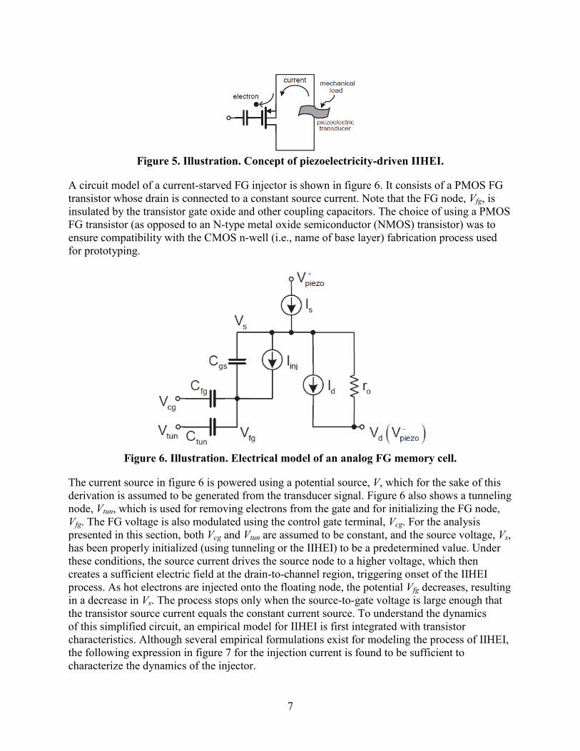
Figure 5. Illustration. Concept of piezoelectricity-driven IIHEI.
A circuit model of a current-starved FG injector is shown in figure 6. It consists of a PMOS FG transistor whose drain is connected to a constant source current. Note that the FG node, Vfg, is insulated by the transistor gate oxide and other coupling capacitors. The choice of using a PMOS FG transistor (as opposed to an N-type metal oxide semiconductor (NMOS) transistor) was to ensure compatibility with the CMOS n-well (i.e., name of base layer) fabrication process used for prototyping.
Figure 6. Illustration. Electrical model of an analog FG memory cell.
The current source in figure 6 is powered using a potential source, V, which for the sake of this derivation is assumed to be generated from the transducer signal. Figure 6 also shows a tunneling node, Vtun, which is used for removing electrons from the gate and for initializing the FG node, Vfg. The FG voltage is also modulated using the control gate terminal, Vcg. For the analysis presented in this section, both Vcg and Vtun are assumed to be constant, and the source voltage, Vs, has been properly initialized (using tunneling or the IIHEI) to be a predetermined value. Under these conditions, the source current drives the source node to a higher voltage, which then creates a sufficient electric field at the drain-to-channel region, triggering onset of the IIHEI process. As hot electrons are injected onto the floating node, the potential Vfg decreases, resulting in a decrease in Vs. The process stops only when the source-to-gate voltage is large enough that the transistor source current equals the constant current source. To understand the dynamics of this simplified circuit, an empirical model for IIHEI is first integrated with transistor characteristics. Although several empirical formulations exist for modeling the process of IIHEI, the following expression in figure 7 for the injection current is found to be sufficient to characterize the dynamics of the injector.

8
sd injV Vinj sI I eβ=
Figure 7. Equation. IIHEI current.
Where:
β and Vinj = Functions of transistor size and process parameters. Is = Source current. Vsd = Source-to-drain voltage.
By controlling the constant current source (also the source current) in figure 6, the FG transistor can be biased in the weak inversion regime. The reason for biasing the transistor in weak inversion is to reduce the power dissipation and obtain a log-linear response (shown in this derivation). In weak inversion, the source current, Is, through the transistor, Mp, can also be expressed as shown in figure 8.
0
fg s
T T
V VU U
sI I e eκ−
= Figure 8. Equation. Source current.
Where:
I0 = Pre-exponential component. Vfg = FG voltage. Vs = Source voltage. κ = FG efficiency. UT = Thermal voltage (26 mV at 300 K).
For the constant source current Is, the relationship between the source voltage and the FG voltage can be obtained from figure 9.
0
ln .s sTfg
V IUVIκ κ
= −
Figure 9. Equation. FG voltage.
Applying figure 9 into figure 7 and expressing the injection current as the change of the FG voltage with respective to time, the equation in figure 10 was created.
0
lns
inj
s sTVVfg
inj t t s
V IUIV
I C C I et t
κ κβ
∂ − ∂ = − = − =
∂ ∂ Figure 10. Equation. Injection current as a function of the FG voltage.
Where:
Ct = Total capacitance of the floating node Vfg.

9
From figure 10, the differential equation for Vs can be expressed using figure 11 and figure 12.
21
sK VsV K et
∂= −
∂ Figure 11. Equation. Differential equation for the source voltage.
1 21, .s
t inj
IK KC Vκβ
= =
Figure 12. Equation. System variables.
Where:
K1 and K2 = Constants.
The general solution of figure 11 can be expressed using the equation in figure 13.
( ) ( )2 01 2
2
1 ln sK VsV t K K t e
K−= − +
Figure 13. Equation. Source voltage as a function of the cumulative duration of the
injection process, t.
Where:
Vs0 = Initial source voltage. t = Cumulative duration of the injection process.
2.2 PRELIMINARY LABORATORY EVALUATION
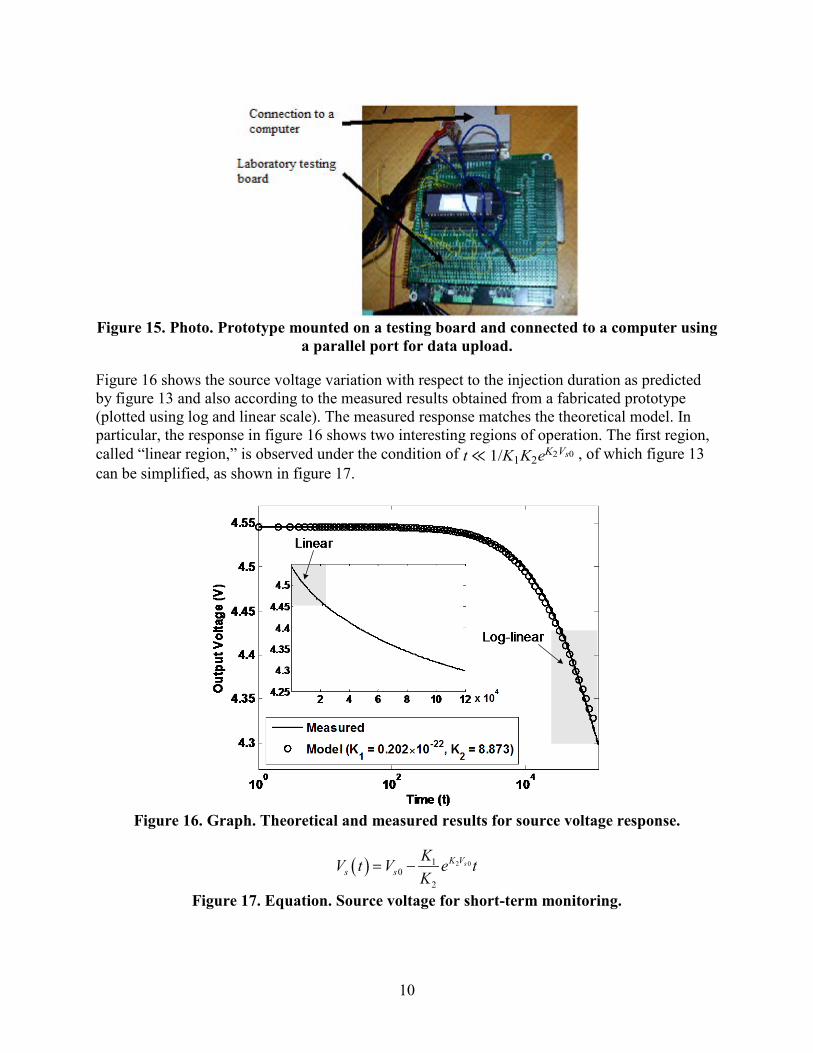
The self-powered sensor design (described in section 2.1) was submitted and manufactured in a standard 0.02-mil (0.5-µm ) CMOS process. Figure 14 shows a prototype chip on a dual in-line package (DIP)40. The actual electronics are included on 0.0015-inch2 (0.9678-mm2) area with silicon at the center. The selected packaging is suitable for laboratory testing and can be easily integrated on a testing board as shown in figure 15. The board was designed and interfaced with a computer. Data are uploaded from the sensor to the database using a MATLAB® program. The wireless interface, designed and integrated on a chip, alleviates the need for a test board. Data can be uploaded directly using a wireless protocol. The test board was used throughout the project as an easy way to manipulate testing support for the developed prototypes. These tests allow for the identification of possible manufacturing mismatches and the verification of all expected basic functionalities of the circuits.
Figure 14. Photo. Sensor prototype manufactured on a DIP40 packaging system.
10
Figure 15. Photo. Prototype mounted on a testing board and connected to a computer using
a parallel port for data upload.
Figure 16 shows the source voltage variation with respect to the injection duration as predicted by figure 13 and also according to the measured results obtained from a fabricated prototype (plotted using log and linear scale). The measured response matches the theoretical model. In particular, the response in figure 16 shows two interesting regions of operation. The first region, called “linear region,” is observed under the condition of t ≪ 1/K1K2eK2Vs0 , of which figure 13 can be simplified, as shown in figure 17.
Figure 16. Graph. Theoretical and measured results for source voltage response.
( ) 2 010
2
sK Vs s
KV t V e tK
= −
Figure 17. Equation. Source voltage for short-term monitoring.

11
Where the approximation ln(1 + x) ≈ x. Figure 17 demonstrates a linear response of the source voltage with respect to the injection duration (see figure 16 inset) and is useful for monitoring short-term events (typically less than a cumulative event duration of 100 s). However, for long-term monitoring, the second region of operation called the “log-linear” region is important and is observed under the condition t ≫ 1 K1K2eK2Vs0⁄ . For log-linear conditions, figure 13 can be simplified to figure 18.
( ) ( ) ( )1 22 2
1 1ln ln .sV t K K tK K
= − −
Figure 18. Equation. Source voltage for long-term monitoring.
Thus, the source voltage is a logarithmic function of injection duration. The response is illustrated in figure 16 using both measured and empirical models where it is shown to be valid for time (t > 1,000 s), and it is the fundamental behavior used for designing event monitoring processors in this research. In fact, the log-linear model is valid beyond 100,000 s, where the injection currents become as small as a single electron per second. This can be readily verified from the measured response in figure 16, where the FG capacitance is 50 fF and the change in voltage observed is 20 mV over duration of 10,000 s. Another interesting result that can be seen from figure 18 is that Vs is independent of its initial value and is only dependent on the two constants, K1 and K2. The slope of the log-linear response is completely determined by 1/K2, while K1 only introduces an offset capturing artifacts arising due to biasing condition, ambient temperature, and CMOS process parameters. Thus, figure 18 also provides a model for compensating these systematic errors using a simple differential offset cancellation technique. Figure 18 can be written in its differential form as figure 19.
( ) 0
2 0
1 lnstV t
K t t
∆ ∆ = + ∆ Figure 19. Equation. Change in source voltage.
Where t0 denotes a reference time with respect to which the differential time intervalΔt is measured.
From figure 19, it is apparent that the differential operation is independent of the parameter K1. Thus, the robustness of sensor performance is directly related to K2. Several experiments were conducted to quantify the robustness of the parameter K2 to different environmental and manufacturing mismatch conditions. Figure 20 shows the responses obtained from multiple memory cells on the same sensor that were biased with different current sources (Is). The mismatch in the parameter (K2) was calculated to be less than 10 percent for a bias current variation greater than 100 percent. The result is encouraging since it implies that the precision of the current source is not critical for the operation of the FG injector.
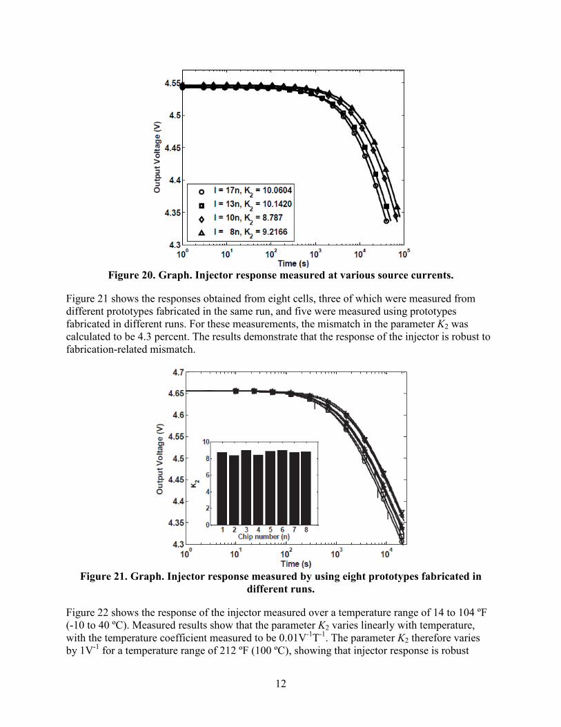
12
Figure 20. Graph. Injector response measured at various source currents.
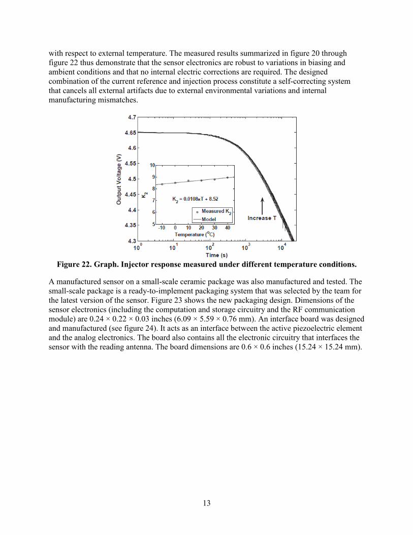
Figure 21 shows the responses obtained from eight cells, three of which were measured from different prototypes fabricated in the same run, and five were measured using prototypes fabricated in different runs. For these measurements, the mismatch in the parameter K2 was calculated to be 4.3 percent. The results demonstrate that the response of the injector is robust to fabrication-related mismatch.
Figure 21. Graph. Injector response measured by using eight prototypes fabricated in
different runs.
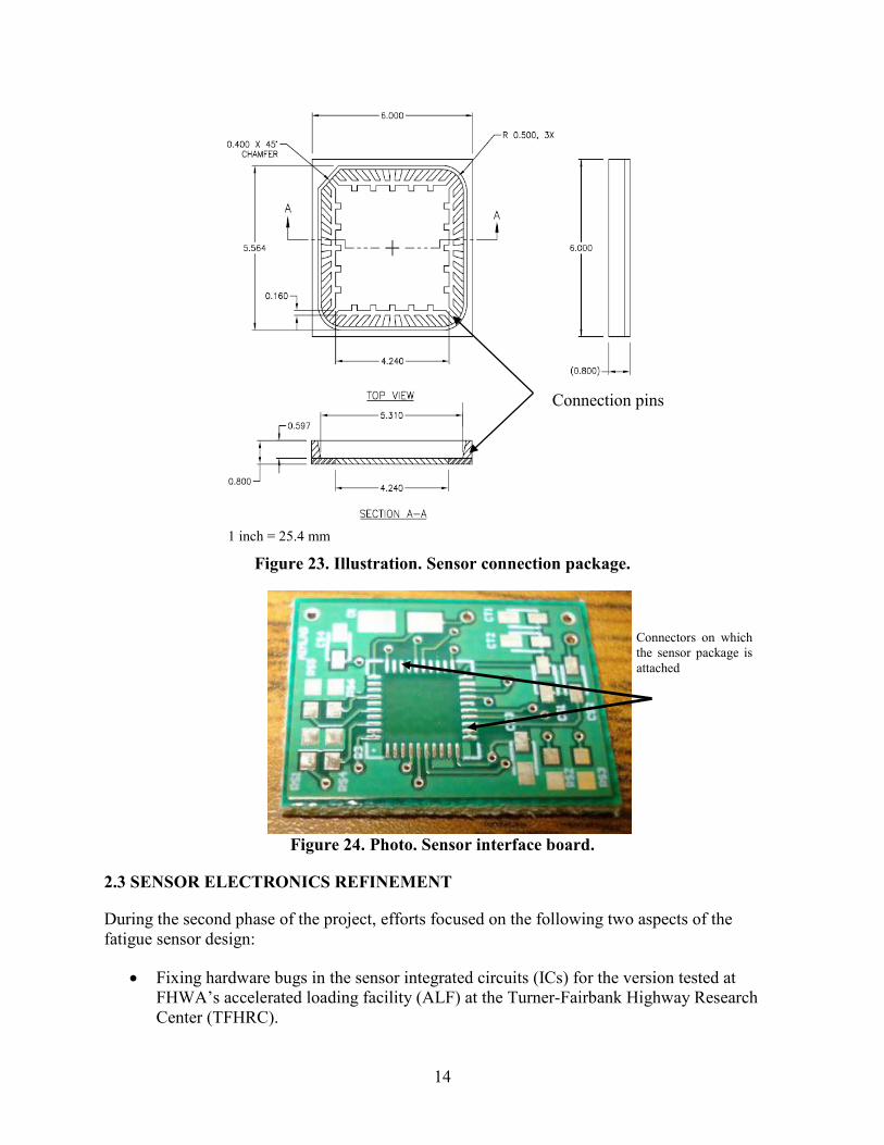
Figure 22 shows the response of the injector measured over a temperature range of 14 to 104 ºF (-10 to 40 ºC). Measured results show that the parameter K2 varies linearly with temperature, with the temperature coefficient measured to be 0.01V-1T-1. The parameter K2 therefore varies by 1V-1 for a temperature range of 212 ºF (100 ºC), showing that injector response is robust
13
with respect to external temperature. The measured results summarized in figure 20 through figure 22 thus demonstrate that the sensor electronics are robust to variations in biasing and ambient conditions and that no internal electric corrections are required. The designed combination of the current reference and injection process constitute a self-correcting system that cancels all external artifacts due to external environmental variations and internal manufacturing mismatches.
Figure 22. Graph. Injector response measured under different temperature conditions.
A manufactured sensor on a small-scale ceramic package was also manufactured and tested. The small-scale package is a ready-to-implement packaging system that was selected by the team for the latest version of the sensor. Figure 23 shows the new packaging design. Dimensions of the sensor electronics (including the computation and storage circuitry and the RF communication module) are 0.24 × 0.22 × 0.03 inches (6.09 × 5.59 × 0.76 mm). An interface board was designed and manufactured (see figure 24). It acts as an interface between the active piezoelectric element and the analog electronics. The board also contains all the electronic circuitry that interfaces the sensor with the reading antenna. The board dimensions are 0.6 × 0.6 inches (15.24 × 15.24 mm).
14
Connection pins
1 inch = 25.4 mm
Figure 23. Illustration. Sensor connection package.
Connectors on which the sensor package is attached
Figure 24. Photo. Sensor interface board.
2.3 SENSOR ELECTRONICS REFINEMENT
During the second phase of the project, efforts focused on the following two aspects of the fatigue sensor design:
• Fixing hardware bugs in the sensor integrated circuits (ICs) for the version tested at FHWA’s accelerated loading facility (ALF) at the Turner-Fairbank Highway Research Center (TFHRC).

15
• Investigating passive matching techniques, which can maximize the powering and reading distance of the sensor given the size constraints.
Table 1 compares the list of hardware changes that were incorporated in different versions of the sensor IC. Version 5.0 refers to the IC that was used in the FHWA field study at the ALF at TFHRC. Version 7.0 refers to the final version of the sensor IC, which incorporates all the major changes from the previous version.
Table 1. Hardware changes that were incorporated in different versions of the sensor IC. Hardware
Change Sensor Version
Version 5 Version 6 Version 7 Version 7(2) FG array Seven-channel
level detection with injection control
Four-channel level and three-channel rate detection with linear injector
Four-channel level and three-channel rate detection with linear injector
Four-channel level and three-channel rate detection with linear injector
RF voltage rectifier
Digital, analog, and FG array
Digital, analog, and FG array
Digital and analog Digital and analog
Ring oscillator With regulator With regulator With regulator With regulator Analog-to-digital converter (ADC)
Fully differential Single-end Single-end, feedback
Single-end, feedback
Switching diode Bulk switching PMOS
Bulk switching PMOS
NMOS NMOS
Protection Not working No RF, piezoelectric RF, piezoelectric Tunneling control No bulk control All bulks short to
ground All bulks short to ground
All bulks short to ground
Pull-down resistor 155 megaohm 188 megaohm Resistor bank Resistor bank Channel reset No With command 01 With command 01 With command 01 Pin number 40 40 40 40 Packaging DIP40 DIP40 DIP40 Quad-flat no-
leads package Load modulation capacitor
Tunable Tunable Tunable Tunable
Status Tested Tested Tested Tested
The important features incorporated in version 7.0 include the following:
• Over-voltage protection for piezoelectric transducer interface—Limits the input voltage to the chip to 9 V.
• On-chip full bridge rectifier—Eliminates the off-chip diodes and reduces the overall power dissipation and sensitivity of the IC.
• Voltage regulation for RF powering—Reduces the variability in the sensor response when powering distance between the reader and the sensor changes.

16
• Eliminating command 06—Eliminates the condition when the sensor state-machine can get stuck in an infinite loop.
• Improving RF clock recovery—Reduces the effect of jitter and improves the performance of the ADCs.
The task of refining the sensor electronics was primarily based on debugging the prototype sensor that was extracted from the field study at TFHRC’s ALF. Even though most of the individual modules on the sensor were found functional post-extraction, the testing revealed the following problems, which were addressed in the subsequent revisions of the sensor:
• After start up, the sensor boots into an undefined state where it continuously transmits invalid data and does not respond to any commands sent by the reader.
• The command received by the sensor and the data transmitted to the reader was found to vary significantly with the distance between the reader and the sensor.
• Many of the received commands were incorrectly decoded by the sensor.
• The resolution of the sensor data received by the reader was found to be less than 5 bits when the ADC resolution was designed to be 8 bits.
The approach used to address these problems included providing worst-case scenario models (e.g., the effect of reader-to-sensor distance) directly into the sensor simulation framework and then verifying if each of the modules are functional. Through this simulation study, significant changes were made to the modules, which are highlighted in red in figure 25. Each of these individual changes is summarized in the following section.
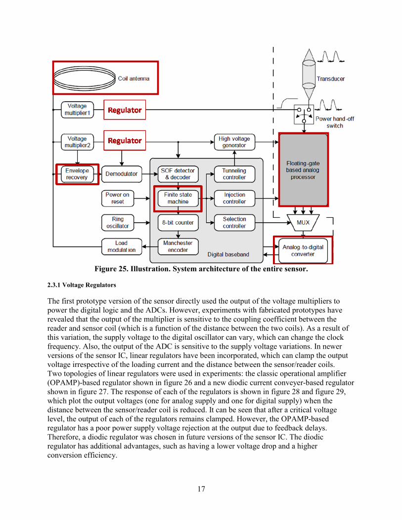
17
Figure 25. Illustration. System architecture of the entire sensor.
2.3.1 Voltage Regulators
The first prototype version of the sensor directly used the output of the voltage multipliers to power the digital logic and the ADCs. However, experiments with fabricated prototypes have revealed that the output of the multiplier is sensitive to the coupling coefficient between the reader and sensor coil (which is a function of the distance between the two coils). As a result of this variation, the supply voltage to the digital oscillator can vary, which can change the clock frequency. Also, the output of the ADC is sensitive to the supply voltage variations. In newer versions of the sensor IC, linear regulators have been incorporated, which can clamp the output voltage irrespective of the loading current and the distance between the sensor/reader coils. Two topologies of linear regulators were used in experiments: the classic operational amplifier (OPAMP)-based regulator shown in figure 26 and a new diodic current conveyer-based regulator shown in figure 27. The response of each of the regulators is shown in figure 28 and figure 29, which plot the output voltages (one for analog supply and one for digital supply) when the distance between the sensor/reader coil is reduced. It can be seen that after a critical voltage level, the output of each of the regulators remains clamped. However, the OPAMP-based regulator has a poor power supply voltage rejection at the output due to feedback delays. Therefore, a diodic regulator was chosen in future versions of the sensor IC. The diodic regulator has additional advantages, such as having a lower voltage drop and a higher conversion efficiency.
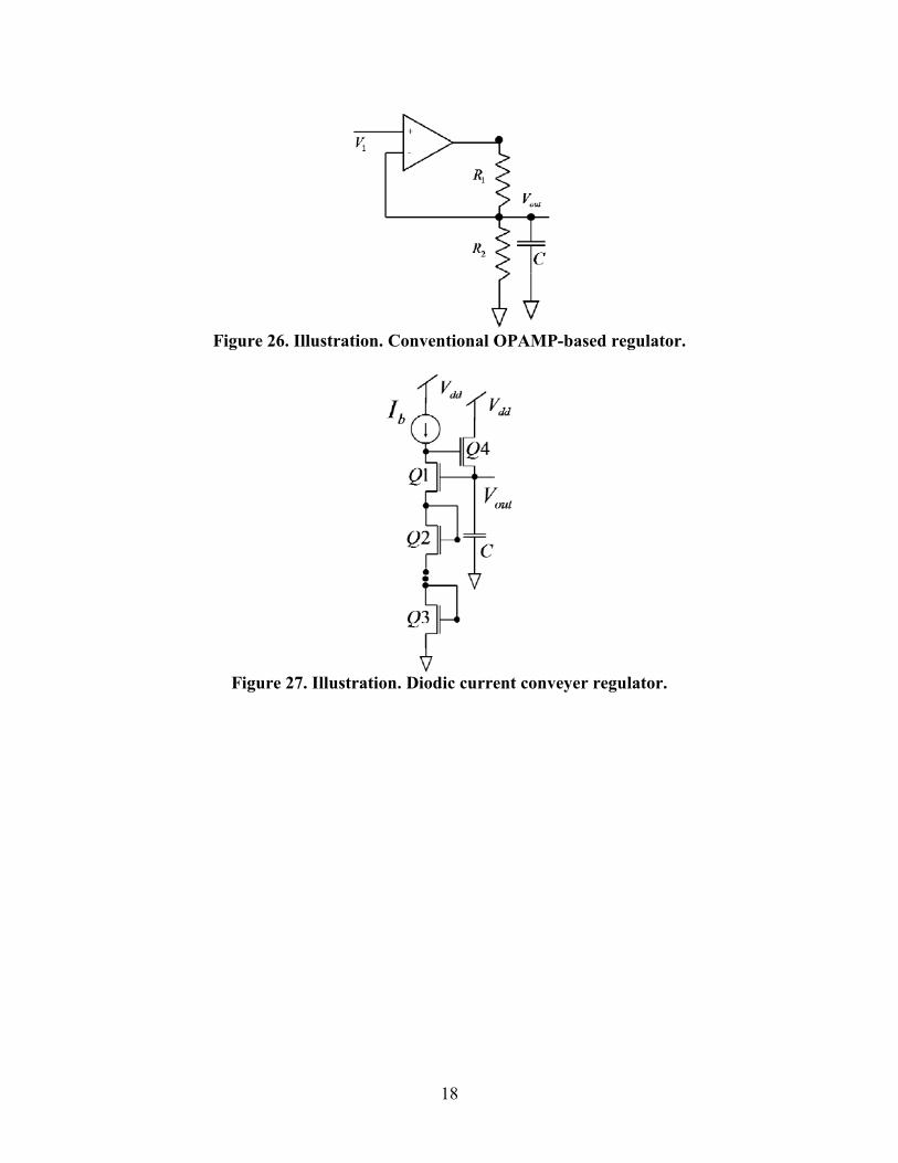
18
Figure 26. Illustration. Conventional OPAMP-based regulator.
Figure 27. Illustration. Diodic current conveyer regulator.
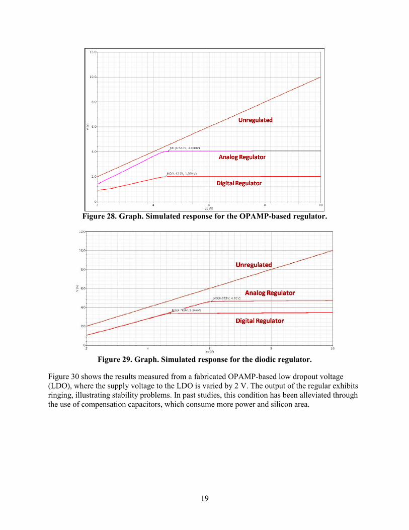
19
Figure 28. Graph. Simulated response for the OPAMP-based regulator.
Figure 29. Graph. Simulated response for the diodic regulator.
Figure 30 shows the results measured from a fabricated OPAMP-based low dropout voltage (LDO), where the supply voltage to the LDO is varied by 2 V. The output of the regular exhibits ringing, illustrating stability problems. In past studies, this condition has been alleviated through the use of compensation capacitors, which consume more power and silicon area.
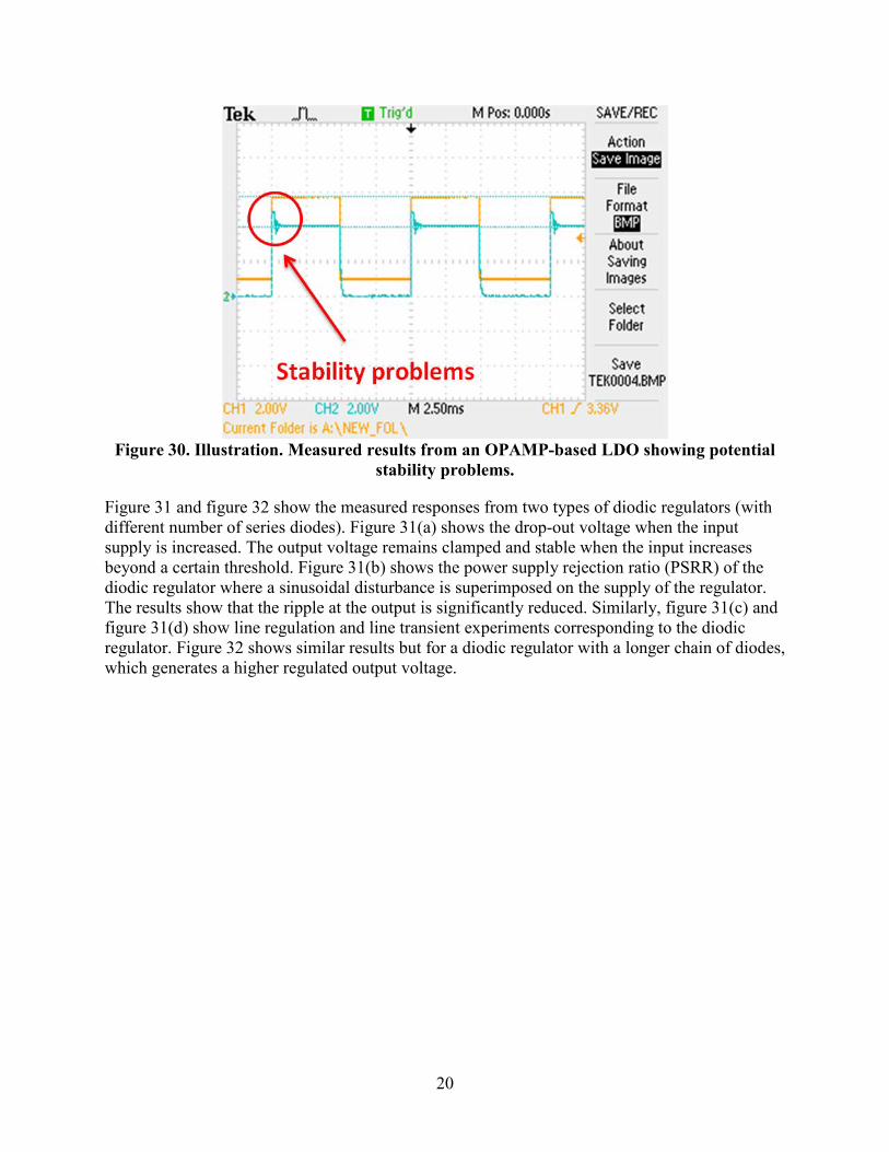
20
Figure 30. Illustration. Measured results from an OPAMP-based LDO showing potential
stability problems.
Figure 31 and figure 32 show the measured responses from two types of diodic regulators (with different number of series diodes). Figure 31(a) shows the drop-out voltage when the input supply is increased. The output voltage remains clamped and stable when the input increases beyond a certain threshold. Figure 31(b) shows the power supply rejection ratio (PSRR) of the diodic regulator where a sinusoidal disturbance is superimposed on the supply of the regulator. The results show that the ripple at the output is significantly reduced. Similarly, figure 31(c) and figure 31(d) show line regulation and line transient experiments corresponding to the diodic regulator. Figure 32 shows similar results but for a diodic regulator with a longer chain of diodes, which generates a higher regulated output voltage.
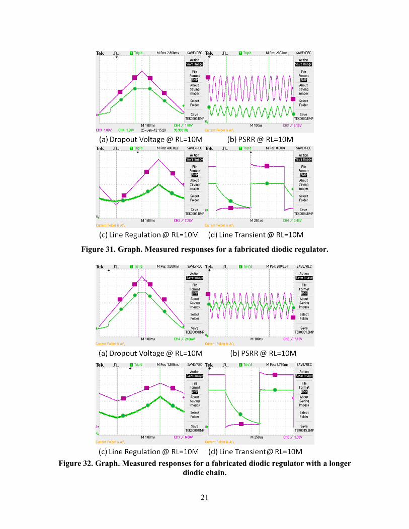
21
Figure 31. Graph. Measured responses for a fabricated diodic regulator.
Figure 32. Graph. Measured responses for a fabricated diodic regulator with a longer
diodic chain.

22
Table 2 summarizes the performance metrics measured from fabricated prototypes of the diodic regulator (with different regulator configuration).
Table 2. Summary of performance metrics of fabricated prototypes.
Version
Input Range (Volts)
Output Range (Volts)
Discharging Time
PSRR at 13.56 MHz
SPS_v008 regulator 1
4.3–10 3.1–3.3 1 ms at RL = 10M 0.3 ms at RL = 1M
-24dB at RL = 10M
SPS_v008 regulator 2
5.7–10 4.2–4.5 1 ms at RL = 10M 0.3 ms at RL = 1M
-28dB at RL = 10M
RFID201107 Reg_Digital
2.7–10 1.96–2.08 2 ms at RL = 10M 0.36 ms at RL = 1M 40 ms at RL = 100K 4.2 ms at RL = 10K
-26dB at RL = 10M -36dB at RL = 1M -29dB at RL = 100K -24dB at RL = 10K
RFID201111 Reg_Ana
4.8–10 3.9–4.0 0.5 ms at RL = 10M -14dB at RL = 10M
RFID201111 Reg_Dig
2.7–10 1.9–2.0 0.5 ms at RL = 10M -16dB at RL = 10M
RL = Remaining life. M = Mega (106). K = Kilo (103).
2.3.2 Additional Changes
Improvements have been made to the ADC by using large-size integrating capacitors and introducing an improved topology of a sample-and-hold circuit, which reduces the effect of channel charge injection and clock feed-through.
One of the primary sources of the data read-out problem was the substrate coupling of 13.56 MHz RF signal to the sensor and in particular to the FGs. One of the solutions to mitigate this problem is to implement an on-chip RF shield, which is difficult because current and ground loops cannot be completely avoided. Therefore, researchers decided to decouple the RF identification (RFID) module from the piezo-powered sensing module and implement the RF powering circuits on a separate silicon substrate. Figure 33 and figure 34 show the layout of two separated modules. Because they do not share a common substrate, the effect of signal coupling is significantly reduced. The RF module is responsible for generating a regulated 2 V supply voltage, which is used by the sensor module for all programming tasks. The communication interface between the two modules is a serial peripheral interface (SPI), which ensures compatibility with the previous sensor versions. An additional benefit of this decoupling is that the sensor module could be interfaced with third party RFID interrogators like an Intel® wireless identification and sensing platform, which hosts a programmable Texas Instruments (TI) MSP430TM microcontroller. This controller could be programmed to generate the SPI command and control required by the sensor module.
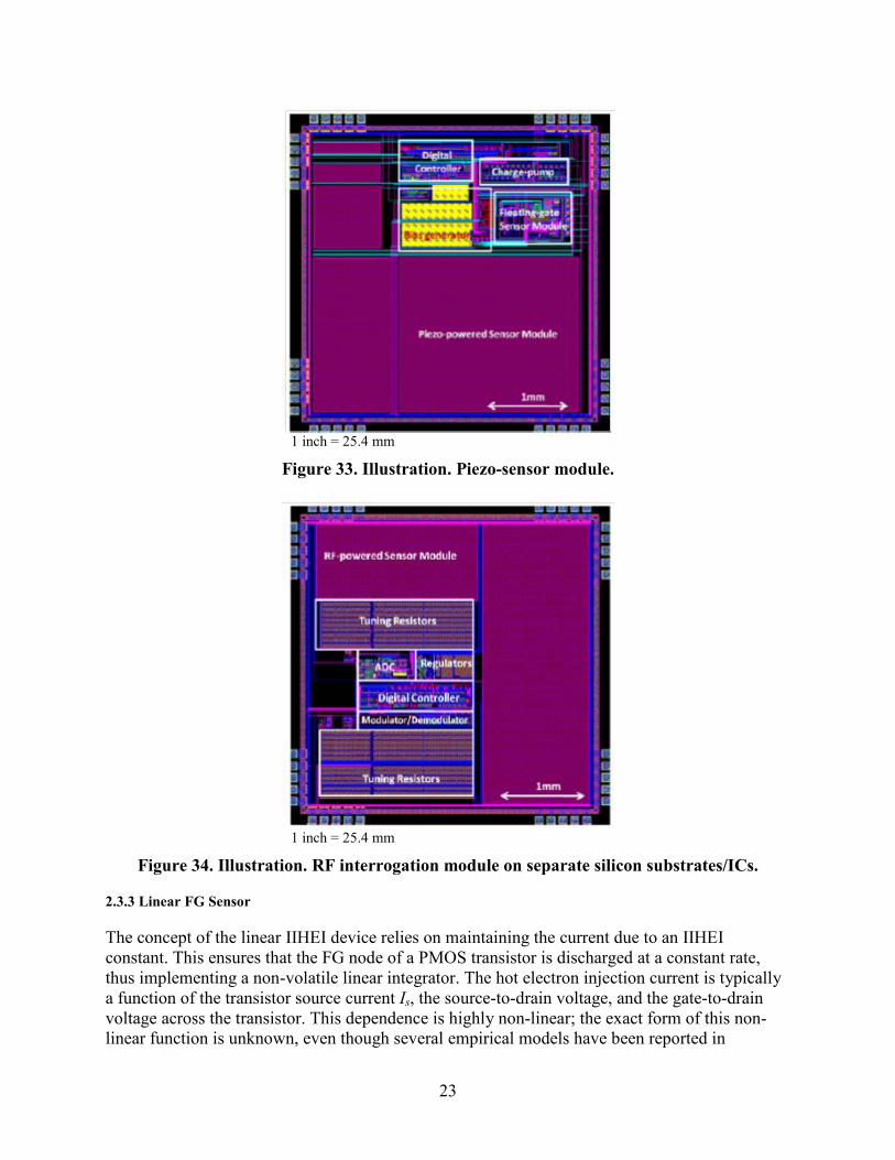
23
1 inch = 25.4 mm
Figure 33. Illustration. Piezo-sensor module.
1 inch = 25.4 mm
Figure 34. Illustration. RF interrogation module on separate silicon substrates/ICs.
2.3.3 Linear FG Sensor
The concept of the linear IIHEI device relies on maintaining the current due to an IIHEI constant. This ensures that the FG node of a PMOS transistor is discharged at a constant rate, thus implementing a non-volatile linear integrator. The hot electron injection current is typically a function of the transistor source current Is, the source-to-drain voltage, and the gate-to-drain voltage across the transistor. This dependence is highly non-linear; the exact form of this non-linear function is unknown, even though several empirical models have been reported in
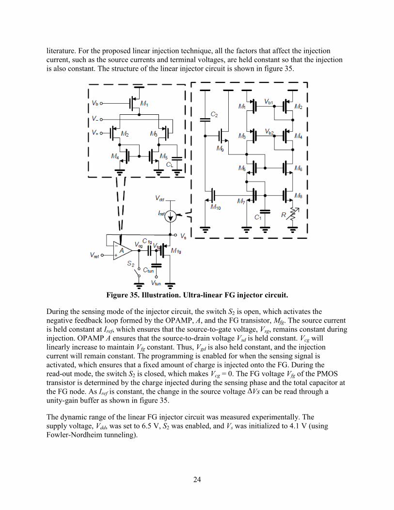
24
literature. For the proposed linear injection technique, all the factors that affect the injection current, such as the source currents and terminal voltages, are held constant so that the injection is also constant. The structure of the linear injector circuit is shown in figure 35.
Figure 35. Illustration. Ultra-linear FG injector circuit.
During the sensing mode of the injector circuit, the switch S2 is open, which activates the negative feedback loop formed by the OPAMP, A, and the FG transistor, Mfg. The source current is held constant at Iref, which ensures that the source-to-gate voltage, Vsg, remains constant during injection. OPAMP A ensures that the source-to-drain voltage Vsd is held constant. Vcg will linearly increase to maintain Vfg constant. Thus, Vgd is also held constant, and the injection current will remain constant. The programming is enabled for when the sensing signal is activated, which ensures that a fixed amount of charge is injected onto the FG. During the read-out mode, the switch S2 is closed, which makes Vcg = 0. The FG voltage Vfg of the PMOS transistor is determined by the charge injected during the sensing phase and the total capacitor at the FG node. As Iref is constant, the change in the source voltage Δ Vs can be read through a unity-gain buffer as shown in figure 35.
The dynamic range of the linear FG injector circuit was measured experimentally. The supply voltage, Vdd, was set to 6.5 V, S2 was enabled, and Vs was initialized to 4.1 V (using Fowler-Nordheim tunneling).
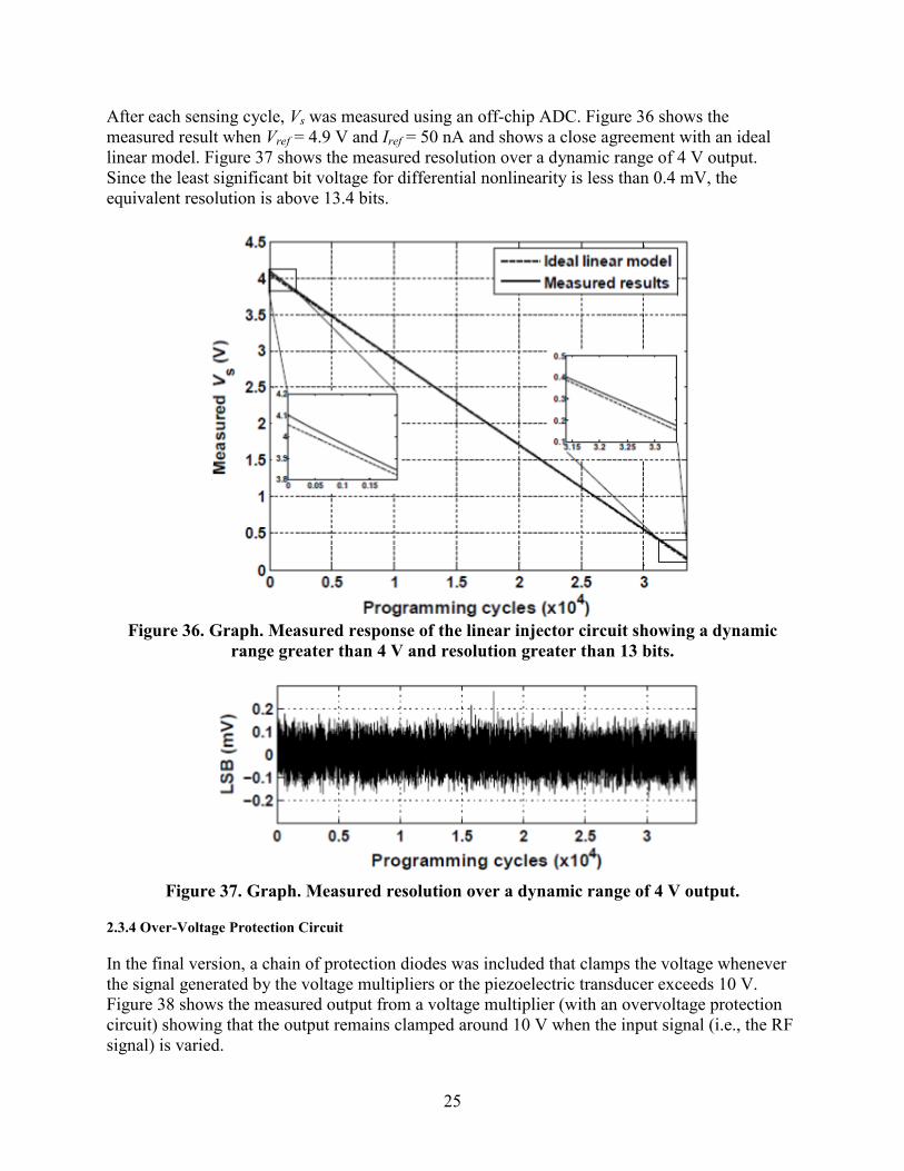
25
After each sensing cycle, Vs was measured using an off-chip ADC. Figure 36 shows the measured result when Vref = 4.9 V and Iref = 50 nA and shows a close agreement with an ideal linear model. Figure 37 shows the measured resolution over a dynamic range of 4 V output. Since the least significant bit voltage for differential nonlinearity is less than 0.4 mV, the equivalent resolution is above 13.4 bits.
Figure 36. Graph. Measured response of the linear injector circuit showing a dynamic
range greater than 4 V and resolution greater than 13 bits.
Figure 37. Graph. Measured resolution over a dynamic range of 4 V output.
2.3.4 Over-Voltage Protection Circuit
In the final version, a chain of protection diodes was included that clamps the voltage whenever the signal generated by the voltage multipliers or the piezoelectric transducer exceeds 10 V. Figure 38 shows the measured output from a voltage multiplier (with an overvoltage protection circuit) showing that the output remains clamped around 10 V when the input signal (i.e., the RF signal) is varied.
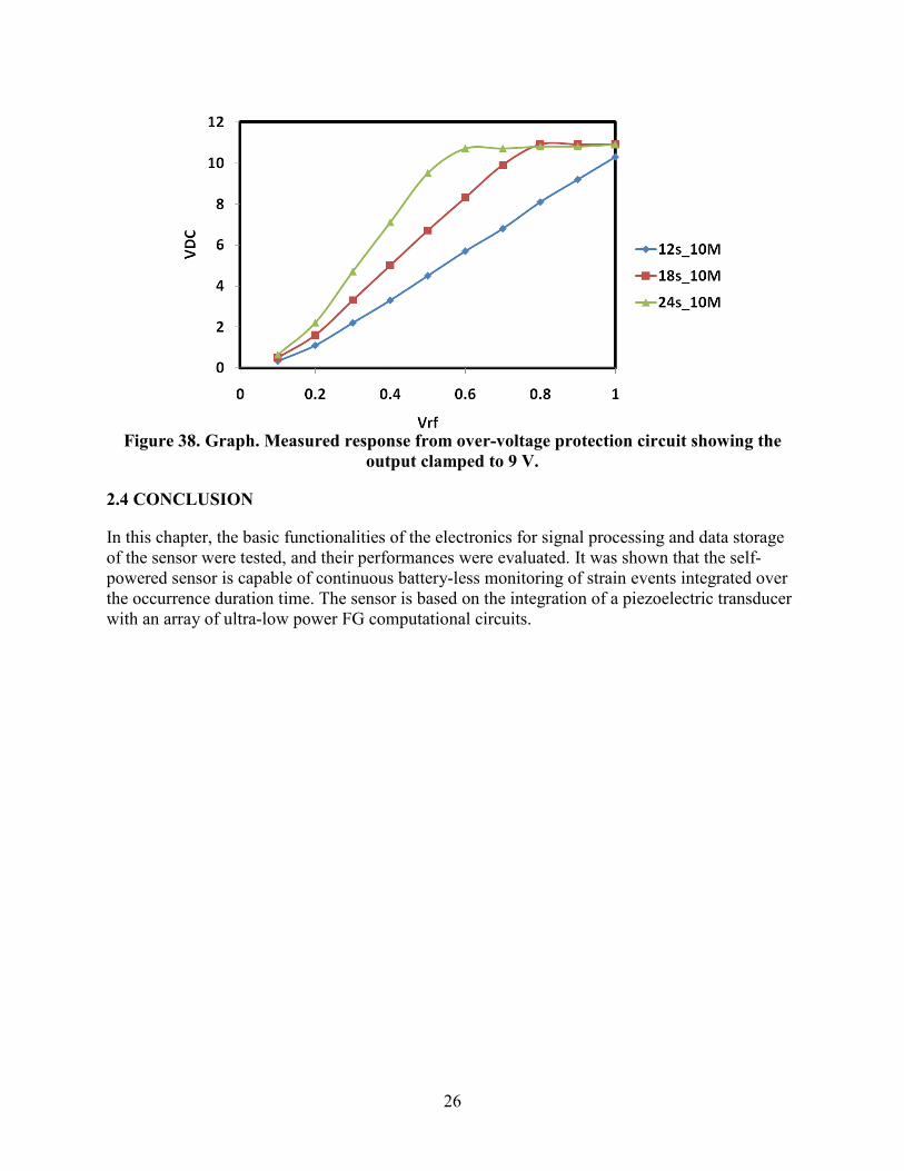
26
Figure 38. Graph. Measured response from over-voltage protection circuit showing the
output clamped to 9 V.
2.4 CONCLUSION
In this chapter, the basic functionalities of the electronics for signal processing and data storage of the sensor were tested, and their performances were evaluated. It was shown that the self-powered sensor is capable of continuous battery-less monitoring of strain events integrated over the occurrence duration time. The sensor is based on the integration of a piezoelectric transducer with an array of ultra-low power FG computational circuits.

27
CHAPTER 3. DEVELOPMENT OF WIRELESS COMMUNICATION AND DATA UPLOAD PROTOCOL
This chapter outlines the development details of an efficient wireless communication protocol between a moveable external reader and the embedded sensors.
3.1 SYSTEM DESIGN
For this project, researchers used an inductive coupling technique for remote RF powering and wireless communication with the sensor. Inductive coupling has been widely used for high-frequency (HF) RFID systems that operate below 30 MHz. The basic principle of inductive coupling is shown in figure 39 and figure 40 where inductor coil L1 is located on the reader and inductor coil L2 is located on the sensor. For this project, the operating frequency was chosen to be 13.56 MHz, which conforms to an existing HF RFID standard. When a 13.56-MHz signal is applied to antenna U1, a time varying magnetic flux is induced across inductor L2, and a voltage U2 is then established at the sensor due to mutual inductance M between the two coils. The mutual inductance M depends on the distance between the two inductors and their dimensions.
Figure 40 shows the equivalent circuit model for the RFID system and the load modulation scheme for wireless communication. R1 and R2 represent the coil resistances. R1, C1, and L1 form a serial resonance circuit for the reader, and R2, C2, and L2 form a parallel resonance circuit for the sensor. The resonance frequency of both circuits is set to be 13.56 MHz, thus maximizing the energy efficiency. The sensor impedance affects the observed voltage U0 at the reader. This voltage can be expressed as the equation in figure 41.
Antennas
Figure 39. Illustration. Principle of HF RFID used in the sensing system.

28
Figure 40. Illustration. Equivalent circuit model for the RFID system and the load
modulation scheme for wireless communication.
U0 = R1i1 + ω2M2
R2+jωL2 + C2RZi1
Figure 41. Equation. Input voltage.
Where:
i1 = Current in the reader resonance circuit. ω = Resonance frequency. RZ = Load resistance.
In the case of ohmic load modulation, a switch, S, is used to change the load resistance of the sensor. Two possible resistance values can be attached to the load, resistor RL (see figure 40), and resistors RL||RM (see figure 40). These two states are used for amplitude shift key (ASK) modulation between the reader and sensor for wireless communication.
3.2 CIRCUIT IMPLEMENTATION
The ASK modulation is achieved with a single NMOS transistor whose gate is connected to the data output of the sensor. In the design, the data are in a serial pattern from the ADC, which samples the source voltage of each FG channel. When data = 0, the NMOS transistor is turned off, and the resistor seen by the reader is Rsensor. When data = 1, the NMOS is turned on and the load resistor becomes 0. The different values of the resistor will change the amplitude of the RF signal. The design of the reader, shown in figure 42, is based on the TRF7960 chip from TI. TRF7960 is a fully integrated 13.56-MHz RFID front-end and data framing reader system. The 13.56-MHz crystal generates the local clock signal for the RF front end. The reader system can transmit the RF signal through the coil to the sensor and sense the variation of the envelope from the sensor part. The reader system is controlled by the field-programmable gate array (FPGA) for setting commands or receiving data.
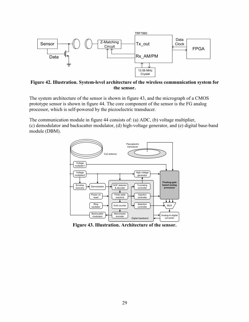
29
Z-Matching Circuit
13.56 MHz Crystal
Tx_out
Rx_AM/PM
FPGA
Data Clock
TRF7960
Sensor
Data
Figure 42. Illustration. System-level architecture of the wireless communication system for
the sensor.
The system architecture of the sensor is shown in figure 43, and the micrograph of a CMOS prototype sensor is shown in figure 44. The core component of the sensor is the FG analog processor, which is self-powered by the piezoelectric transducer.
The communication module in figure 44 consists of: (a) ADC, (b) voltage multiplier, (c) demodulator and backscatter modulator, (d) high-voltage generator, and (e) digital base-band module (DBM).
Voltage multiplier2
Voltage multiplier1
Envelop recovery Demodulator
Power on reset
Ring oscillator
Digital baseband
Floating-gate based analog
processor
Analog-to-digital converter
Manchester encoder
SOF detector & decoder
Finite state machine
8-bit counter
Injection controller
Tunneling controller
Selection controller
High voltage generator
Backscatter modulator
MUX
Coil antenna
Piezoelectric transducer
Figure 43. Illustration. Architecture of the sensor.
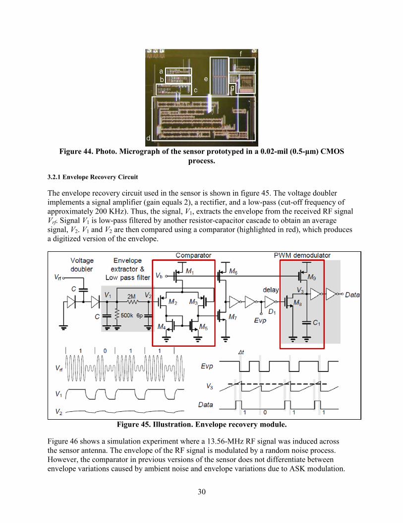
30
Figure 44. Photo. Micrograph of the sensor prototyped in a 0.02-mil (0.5-μm ) CMOS
process.
3.2.1 Envelope Recovery Circuit
The envelope recovery circuit used in the sensor is shown in figure 45. The voltage doubler implements a signal amplifier (gain equals 2), a rectifier, and a low-pass (cut-off frequency of approximately 200 KHz). Thus, the signal, V1, extracts the envelope from the received RF signal Vrf. Signal V1 is low-pass filtered by another resistor-capacitor cascade to obtain an average signal, V2. V1 and V2 are then compared using a comparator (highlighted in red), which produces a digitized version of the envelope.
Figure 45. Illustration. Envelope recovery module.
Figure 46 shows a simulation experiment where a 13.56-MHz RF signal was induced across the sensor antenna. The envelope of the RF signal is modulated by a random noise process. However, the comparator in previous versions of the sensor does not differentiate between envelope variations caused by ambient noise and envelope variations due to ASK modulation.
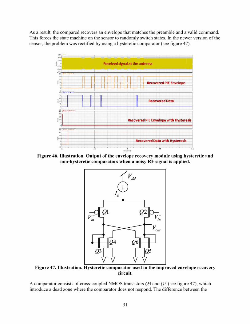
31
As a result, the compared recovers an envelope that matches the preamble and a valid command. This forces the state machine on the sensor to randomly switch states. In the newer version of the sensor, the problem was rectified by using a hysteretic comparator (see figure 47).
Figure 46. Illustration. Output of the envelope recovery module using hysteretic and
non-hysteretic comparators when a noisy RF signal is applied.
Figure 47. Illustration. Hysteretic comparator used in the improved envelope recovery
circuit.
A comparator consists of cross-coupled NMOS transistors Q4 and Q5 (see figure 47), which introduce a dead zone where the comparator does not respond. The difference between the
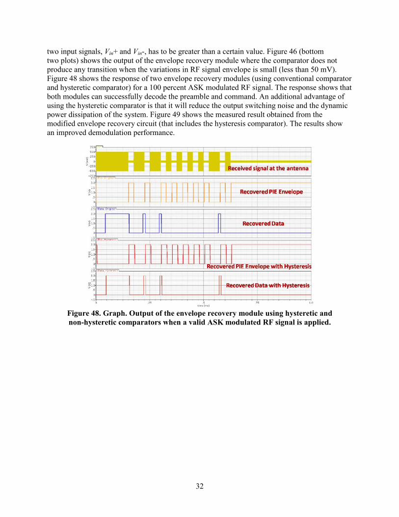
32
two input signals, Vin+ and Vin-, has to be greater than a certain value. Figure 46 (bottom two plots) shows the output of the envelope recovery module where the comparator does not produce any transition when the variations in RF signal envelope is small (less than 50 mV). Figure 48 shows the response of two envelope recovery modules (using conventional comparator and hysteretic comparator) for a 100 percent ASK modulated RF signal. The response shows that both modules can successfully decode the preamble and command. An additional advantage of using the hysteretic comparator is that it will reduce the output switching noise and the dynamic power dissipation of the system. Figure 49 shows the measured result obtained from the modified envelope recovery circuit (that includes the hysteresis comparator). The results show an improved demodulation performance.
Figure 48. Graph. Output of the envelope recovery module using hysteretic and non-hysteretic comparators when a valid ASK modulated RF signal is applied.
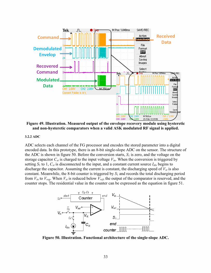
33
Figure 49. Illustration. Measured output of the envelope recovery module using hysteretic
and non-hysteretic comparators when a valid ASK modulated RF signal is applied.
3.2.2 ADC
ADC selects each channel of the FG processor and encodes the stored parameter into a digital encoded data. In this prototype, there is an 8-bit single-slope ADC on the sensor. The structure of the ADC is shown in figure 50. Before the conversion starts, S1 is zero, and the voltage on the storage capacitor Cst is charged to the input voltage Vin. When the conversion is triggered by setting S1 to 1, Cst is disconnected to the input, and a constant current source Idis begins to discharge the capacitor. Assuming the current is constant, the discharging speed of Vst is also constant. Meanwhile, the 8-bit counter is triggered by S1 and records the total discharging period from Vin to Vreg. When Vst is reduced below Vref, the output of the comparator is reserved, and the counter stops. The residential value in the counter can be expressed as the equation in figure 51.
Figure 50. Illustration. Functional architecture of the single-slope ADC.
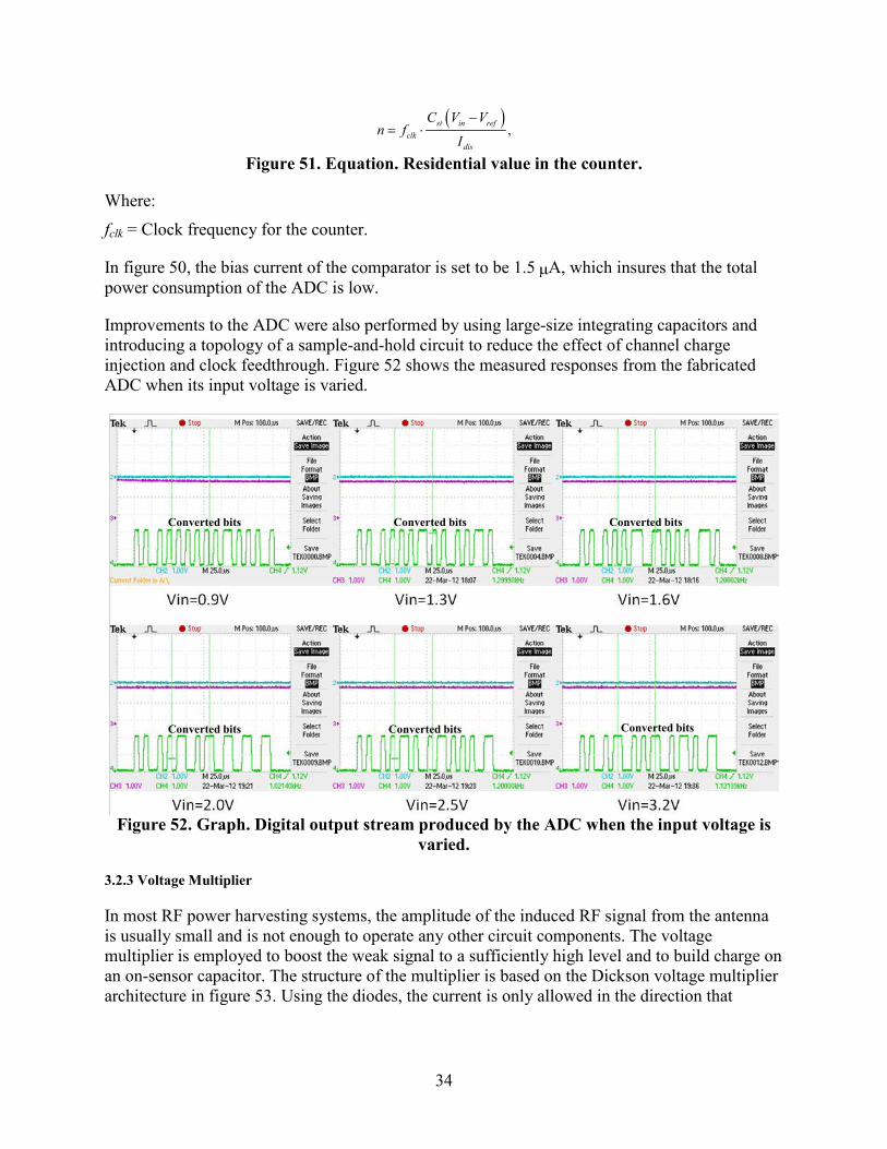
34
( ),st in ref
clkdis
C V Vn f
I−
= ⋅
Figure 51. Equation. Residential value in the counter.
Where:
fclk = Clock frequency for the counter.
In figure 50, the bias current of the comparator is set to be 1.5 µ A, which insures that the total power consumption of the ADC is low.
Improvements to the ADC were also performed by using large-size integrating capacitors and introducing a topology of a sample-and-hold circuit to reduce the effect of channel charge injection and clock feedthrough. Figure 52 shows the measured responses from the fabricated ADC when its input voltage is varied.
Converted bitsConverted bitsConverted bits
Converted bits Converted bits Converted bits
Figure 52. Graph. Digital output stream produced by the ADC when the input voltage is
varied.
3.2.3 Voltage Multiplier
In most RF power harvesting systems, the amplitude of the induced RF signal from the antenna is usually small and is not enough to operate any other circuit components. The voltage multiplier is employed to boost the weak signal to a sufficiently high level and to build charge on an on-sensor capacitor. The structure of the multiplier is based on the Dickson voltage multiplier architecture in figure 53. Using the diodes, the current is only allowed in the direction that

35
charges the capacitor in the next stage. For a multiple-stage voltage multiplier, the output voltage can be expressed as shown in figure 54.
Figure 53. Illustration. Structure of the Dickson voltage multiplier.
,out rf on loadpar
CV N V V VC C
= ⋅ − − +
Figure 54. Equation. Output voltage.
Where:
C = Storage capacitor. Cpar = Parasitic capacitor. Von = Turn-on voltage for the diode. Vload = Additional voltage drop depending on the load current.
The induced RF signal Vrf is typically less than 1 V. As a result, diodes with large turn-on voltage significantly decrease the generated voltage. The diode is usually replaced by a diode-connected transistor in the design, so a low-threshold or zero-threshold transistor is preferred for the voltage multiplier. When the low-threshold process is not available, using a Schottky diode is another option to reduce Von. A group of Schottky diodes with a different number of fingers and same junction area have been fabricated in a 0.02-mil (0.5-µm ) standard CMOS process. The diode with more fingers shows smaller Von due to the reduction of the parasitic resistor. However, the reversed current will also increase for the diode with more fingers. All the turn-on voltages for Schottky diodes are measured to be close to 300 mV, which is much less than Vth for the process (0.7 for NMOS and -0.9 for PMOS).
3.2.4 Demodulator and Backscatter Modulator
The demodulator module on the sensor is used to acquire command and control information (also known as forward link) from the reader, whereas the backscatter modulator is used to modulate the impedance of the coil and establish a reverse link communication from the sensor to the reader. The system architecture implementing the demodulator and backscatter modulator is shown in figure 55. In the forward link from the reader to the sensor, a pulse width modulation (PWM) approach is used, where a pulse width of 75 ms indicates 1 and a pulse width of 50 ms indicates 0. When the reader is sending a command, the variation on the RF envelope can be detected. The recovered pulse signal itself resets the integrator and generates a different level according to the pulse width. Afterwards, a level crossing decodes the received bit. For the backward link from sensor to reader, a simple backscatter scheme is applied. After the voltage is
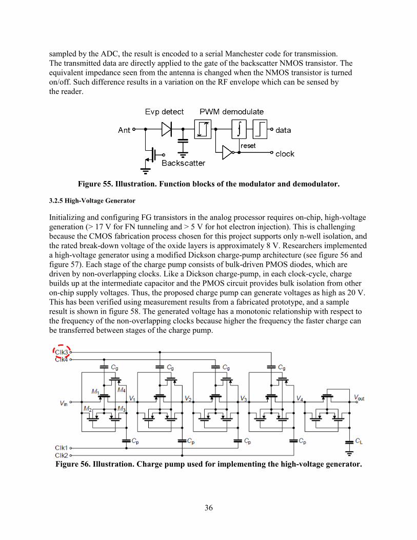
36
sampled by the ADC, the result is encoded to a serial Manchester code for transmission. The transmitted data are directly applied to the gate of the backscatter NMOS transistor. The equivalent impedance seen from the antenna is changed when the NMOS transistor is turned on/off. Such difference results in a variation on the RF envelope which can be sensed by the reader.
Figure 55. Illustration. Function blocks of the modulator and demodulator.
3.2.5 High-Voltage Generator
Initializing and configuring FG transistors in the analog processor requires on-chip, high-voltage generation (> 17 V for FN tunneling and > 5 V for hot electron injection). This is challenging because the CMOS fabrication process chosen for this project supports only n-well isolation, and the rated break-down voltage of the oxide layers is approximately 8 V. Researchers implemented a high-voltage generator using a modified Dickson charge-pump architecture (see figure 56 and figure 57). Each stage of the charge pump consists of bulk-driven PMOS diodes, which are driven by non-overlapping clocks. Like a Dickson charge-pump, in each clock-cycle, charge builds up at the intermediate capacitor and the PMOS circuit provides bulk isolation from other on-chip supply voltages. Thus, the proposed charge pump can generate voltages as high as 20 V. This has been verified using measurement results from a fabricated prototype, and a sample result is shown in figure 58. The generated voltage has a monotonic relationship with respect to the frequency of the non-overlapping clocks because higher the frequency the faster charge can be transferred between stages of the charge pump.
Figure 56. Illustration. Charge pump used for implementing the high-voltage generator.
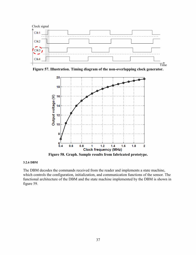
37
Time
Clock signal
Figure 57. Illustration. Timing diagram of the non-overlapping clock generator.
Figure 58. Graph. Sample results from fabricated prototype.
3.2.6 DBM
The DBM decodes the commands received from the reader and implements a state machine, which controls the configuration, initialization, and communication functions of the sensor. The functional architecture of the DBM and the state machine implemented by the DBM is shown in figure 59.

38
Figure 59. Illustration. State machine implemented by DBM.
The state machine is implemented with standard CMOS logic, and the architecture has been synthesized using the standard logic synthesis procedure. By default, the state machine is in its ideal state, S0. Transition to the other states (S1–S5) occurs when a valid command is received from the reader. The validity of the command is confirmed when the data packet transmitted from the reader is Manchester encoded and satisfies the parity check condition.
3.3 TESTING PROCEDURES AND MEASURED RESULTS
Prototype sensor ICs have been fabricated in a 0.02-mil (0.5-µm ) standard CMOS process. The total area of the sensor IC is 0.06 × 0.06 inches (1.52 × 1.52 mm), which was then integrated on a custom-made printed circuit board (PCB) as shown in figure 60. In order to optimize the power transfer and increase the reading distance, an external reader was designed and manufactured (see figure 60). The design is based on a commercial chip TRF7960 from TI, which is a fully integrated 13.56-MHz RFID analog front-end system. The TI chip is controlled by an FPGA that has been programmed for data encoding and decoding. The reader interfaces with an embedded antenna, which fits the exact H-shape of the designed package, thus establishing a link for data transfer (the embedded antenna is shown in figure 61). The antenna is connected to the board shown in figure 60 along with the external reader to illustrate the size difference. Laboratory testing showed that the reading distance highly depends on the parasitic capacitances of the antennas and the manufactured sensor, varying between 1 and 13 inches (25.4 and 330.2 mm). These capacitances are manufacturing process dependent. As a result, individual calibration is required as well as testing under field conditions in order to assess the exact performance.
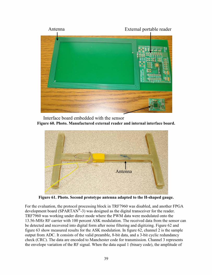
39
External portable reader Antenna
Interface board embedded with the sensor Figure 60. Photo. Manufactured external reader and internal interface board.
Antenna
Figure 61. Photo. Second prototype antenna adapted to the H-shaped gauge.
For the evaluation, the protocol processing block in TRF7960 was disabled, and another FPGA development board (SPARTAN®-3) was designed as the digital transceiver for the reader. TRF7960 was working under direct mode where the PWM data were modulated onto the 13.56-MHz RF carrier with 100 percent ASK modulation. The received data from the sensor can be detected and recovered into digital form after noise filtering and digitizing. Figure 62 and figure 63 show measured results for the ASK modulation. In figure 62, channel 2 is the sample output from ADC. It consists of the valid preamble, 8-bit data, and a 3-bit cyclic redundancy check (CRC). The data are encoded to Manchester code for transmission. Channel 3 represents the envelope variation of the RF signal. When the data equal 1 (binary code), the amplitude of
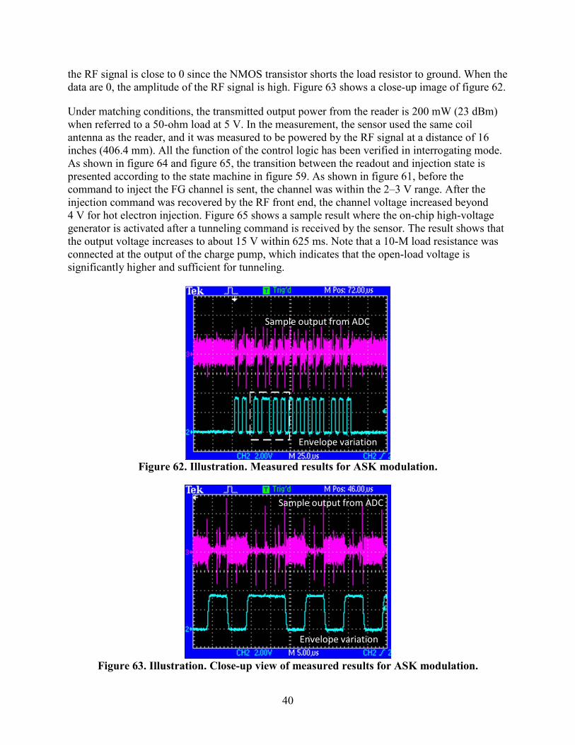
40
the RF signal is close to 0 since the NMOS transistor shorts the load resistor to ground. When the data are 0, the amplitude of the RF signal is high. Figure 63 shows a close-up image of figure 62.
Under matching conditions, the transmitted output power from the reader is 200 mW (23 dBm) when referred to a 50-ohm load at 5 V. In the measurement, the sensor used the same coil antenna as the reader, and it was measured to be powered by the RF signal at a distance of 16 inches (406.4 mm). All the function of the control logic has been verified in interrogating mode. As shown in figure 64 and figure 65, the transition between the readout and injection state is presented according to the state machine in figure 59. As shown in figure 61, before the command to inject the FG channel is sent, the channel was within the 2–3 V range. After the injection command was recovered by the RF front end, the channel voltage increased beyond 4 V for hot electron injection. Figure 65 shows a sample result where the on-chip high-voltage generator is activated after a tunneling command is received by the sensor. The result shows that the output voltage increases to about 15 V within 625 ms. Note that a 10-M load resistance was connected at the output of the charge pump, which indicates that the open-load voltage is significantly higher and sufficient for tunneling.
Sample output from ADC
Envelope variation
Figure 62. Illustration. Measured results for ASK modulation.
Sample output from ADC
Envelope variation
Figure 63. Illustration. Close-up view of measured results for ASK modulation.
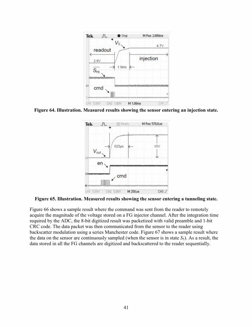
41
Figure 64. Illustration. Measured results showing the sensor entering an injection state.
Figure 65. Illustration. Measured results showing the sensor entering a tunneling state.
Figure 66 shows a sample result where the command was sent from the reader to remotely acquire the magnitude of the voltage stored on a FG injector channel. After the integration time required by the ADC, the 8-bit digitized result was packetized with valid preamble and 1-bit CRC code. The data packet was then communicated from the sensor to the reader using backscatter modulation using a series Manchester code. Figure 67 shows a sample result where the data on the sensor are continuously sampled (when the sensor is in state S5). As a result, the data stored in all the FG channels are digitized and backscattered to the reader sequentially.
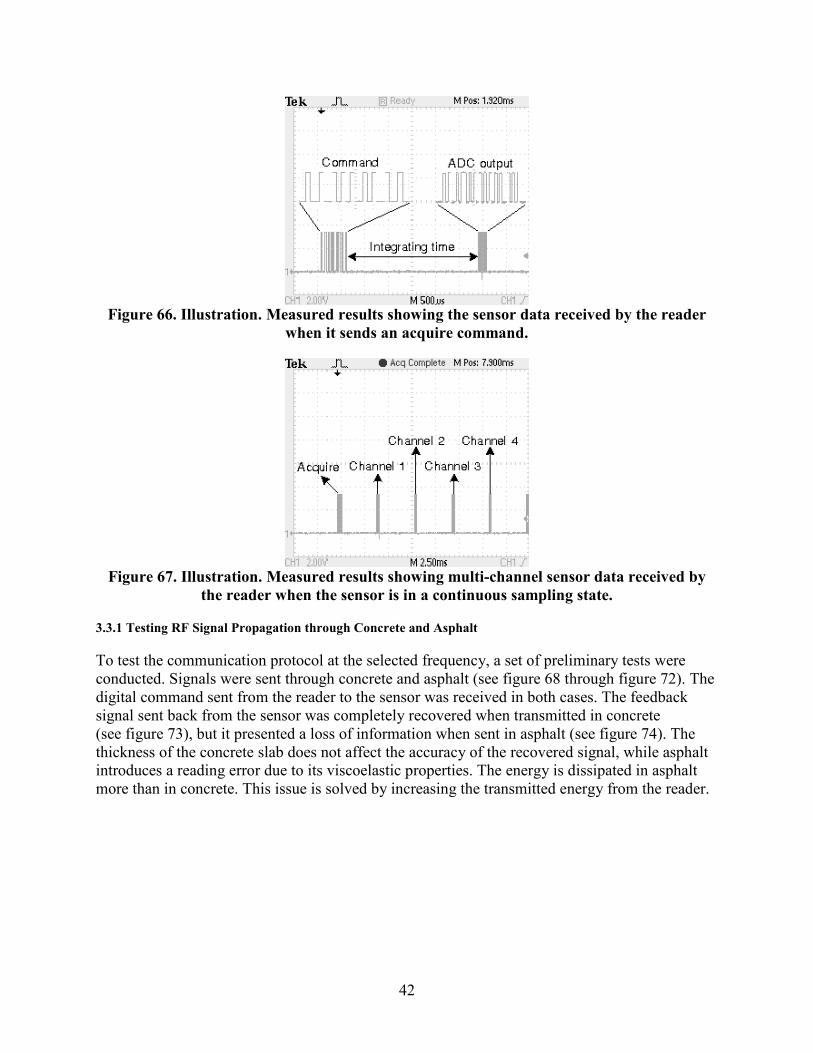
42
Figure 66. Illustration. Measured results showing the sensor data received by the reader
when it sends an acquire command.
Figure 67. Illustration. Measured results showing multi-channel sensor data received by
the reader when the sensor is in a continuous sampling state.
3.3.1 Testing RF Signal Propagation through Concrete and Asphalt
To test the communication protocol at the selected frequency, a set of preliminary tests were conducted. Signals were sent through concrete and asphalt (see figure 68 through figure 72). The digital command sent from the reader to the sensor was received in both cases. The feedback signal sent back from the sensor was completely recovered when transmitted in concrete (see figure 73), but it presented a loss of information when sent in asphalt (see figure 74). The thickness of the concrete slab does not affect the accuracy of the recovered signal, while asphalt introduces a reading error due to its viscoelastic properties. The energy is dissipated in asphalt more than in concrete. This issue is solved by increasing the transmitted energy from the reader.
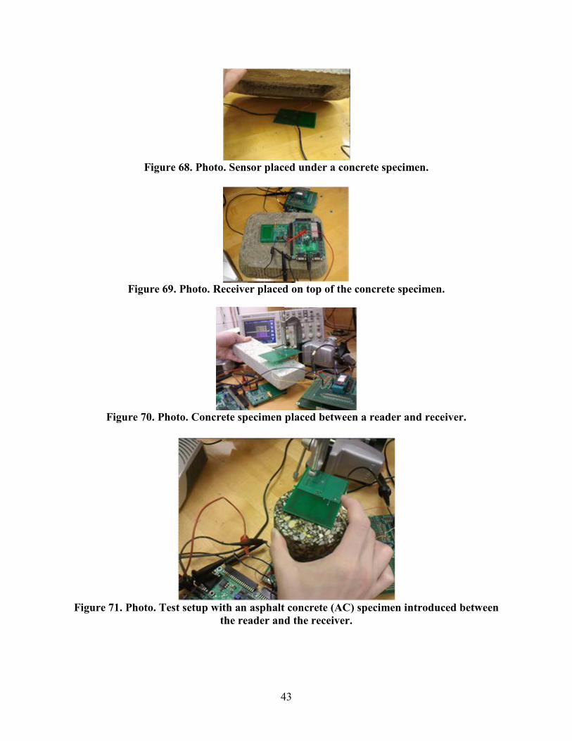
43
Figure 68. Photo. Sensor placed under a concrete specimen.
Figure 69. Photo. Receiver placed on top of the concrete specimen.
Figure 70. Photo. Concrete specimen placed between a reader and receiver.
Figure 71. Photo. Test setup with an asphalt concrete (AC) specimen introduced between
the reader and the receiver.
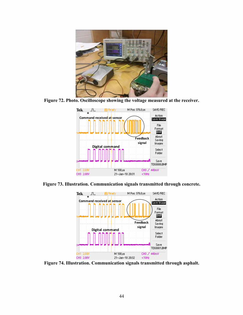
44
Figure 72. Photo. Oscilloscope showing the voltage measured at the receiver.
Digital command
Command received at sensor
Feedbacksignal
Figure 73. Illustration. Communication signals transmitted through concrete.
Digital command
Command received at sensor
Feedbacksignal
Figure 74. Illustration. Communication signals transmitted through asphalt.

45
3.4 CHALLENGES AND IMPLEMENTED SOLUTIONS
As anticipated, the system integration of the sensor and the wireless communication protocol was one of the most challenging tasks in this study. Given the unique nature of the sensing system and based on analog FGs, an adapted and equally unique wireless protocol was completely designed and tested.
A major glitch in the high-voltage generation module caused delays, given that several versions had to be manufactured and tested. The CMOS fabrication process used for this project supports only n-well isolation, and the rated break-down voltage of the oxide layers is approximately 8 V, preventing the generation of the 18 V required for the initialization of the memory gates. After several iterations, a successful design was achieved (details are described in section 3.2.4).
As shown in figure 60 and figure 61, specific antennas were designed and manufactured for this particular system (commercially available antennas and readers cannot be used because of the low power levels at which the sensor operates). The reading distance from the sensor depends on the tuning of the wireless links for maximum power transfer, which depends on the parasitic capacitances of the antennas (embedded antenna and external reader) as well as the parasitic capacitance at the sensors’ input. These capacitances are induced by the manufacturing process. The reading distance at which the system can operate (and thus the installation strategy) depends on the tuning outcome under specific field conditions.
3.4.1 RF Matching Network
Some research focused on optimizing the matching network that can maximize the read and powering distance to the sensor. The design flow is summarized in figure 75, where Rs, RL, and CL denote the reader impedance, sensor load resistance, and sensor load capacitance, respectively. Q_reader and Q_tag denote the quality (Q)-factor of the reader and the sensor, which, in-turn, determines the sensitivity of the reader. Vr, Ir, Vt, It, PRs, and PRL denote the internal electrical variables (voltage, current, and power) at the reader and sensor based on the antenna dimensions, structure, and material properties including the propagation properties of the ambient environment.
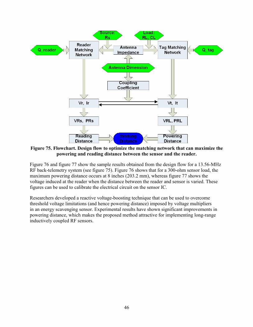
46
Figure 75. Flowchart. Design flow to optimize the matching network that can maximize the
powering and reading distance between the sensor and the reader.
Figure 76 and figure 77 show the sample results obtained from the design flow for a 13.56-MHz RF back-telemetry system (see figure 75). Figure 76 shows that for a 300-ohm sensor load, the maximum powering distance occurs at 8 inches (203.2 mm), whereas figure 77 shows the voltage induced at the reader when the distance between the reader and sensor is varied. These figures can be used to calibrate the electrical circuit on the sensor IC.
Researchers developed a reactive voltage-boosting technique that can be used to overcome threshold voltage limitations (and hence powering distance) imposed by voltage multipliers in an energy scavenging sensor. Experimental results have shown significant improvements in powering distance, which makes the proposed method attractive for implementing long-range inductively coupled RF sensors.
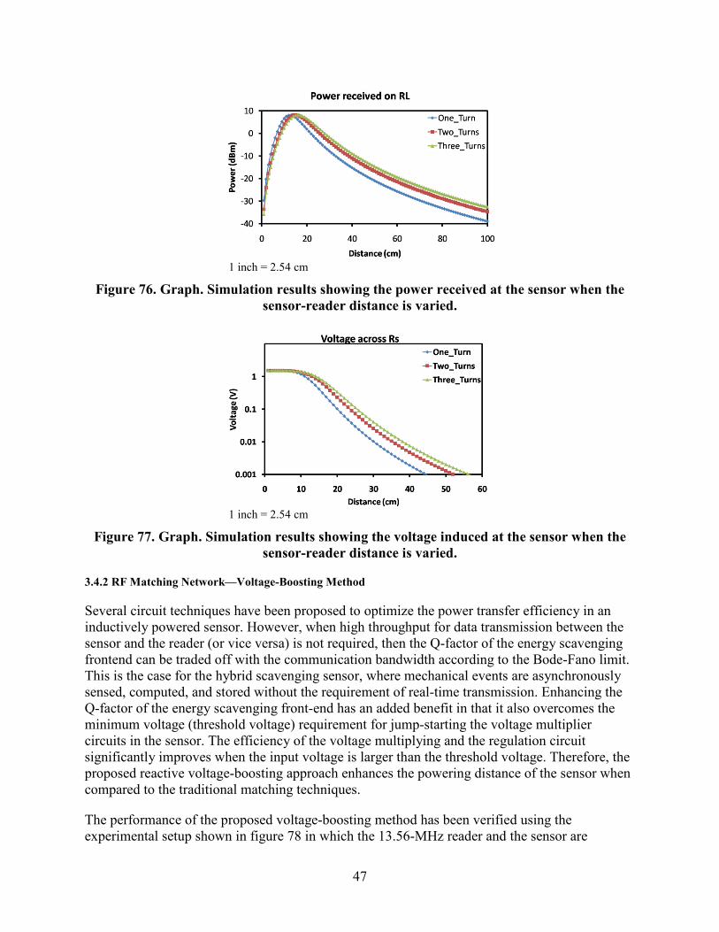
47
1 inch = 2.54 cm
Figure 76. Graph. Simulation results showing the power received at the sensor when the sensor-reader distance is varied.
1 inch = 2.54 cm
Figure 77. Graph. Simulation results showing the voltage induced at the sensor when the sensor-reader distance is varied.
3.4.2 RF Matching Network—Voltage-Boosting Method
Several circuit techniques have been proposed to optimize the power transfer efficiency in an inductively powered sensor. However, when high throughput for data transmission between the sensor and the reader (or vice versa) is not required, then the Q-factor of the energy scavenging frontend can be traded off with the communication bandwidth according to the Bode-Fano limit. This is the case for the hybrid scavenging sensor, where mechanical events are asynchronously sensed, computed, and stored without the requirement of real-time transmission. Enhancing the Q-factor of the energy scavenging front-end has an added benefit in that it also overcomes the minimum voltage (threshold voltage) requirement for jump-starting the voltage multiplier circuits in the sensor. The efficiency of the voltage multiplying and the regulation circuit significantly improves when the input voltage is larger than the threshold voltage. Therefore, the proposed reactive voltage-boosting approach enhances the powering distance of the sensor when compared to the traditional matching techniques.
The performance of the proposed voltage-boosting method has been verified using the experimental setup shown in figure 78 in which the 13.56-MHz reader and the sensor are
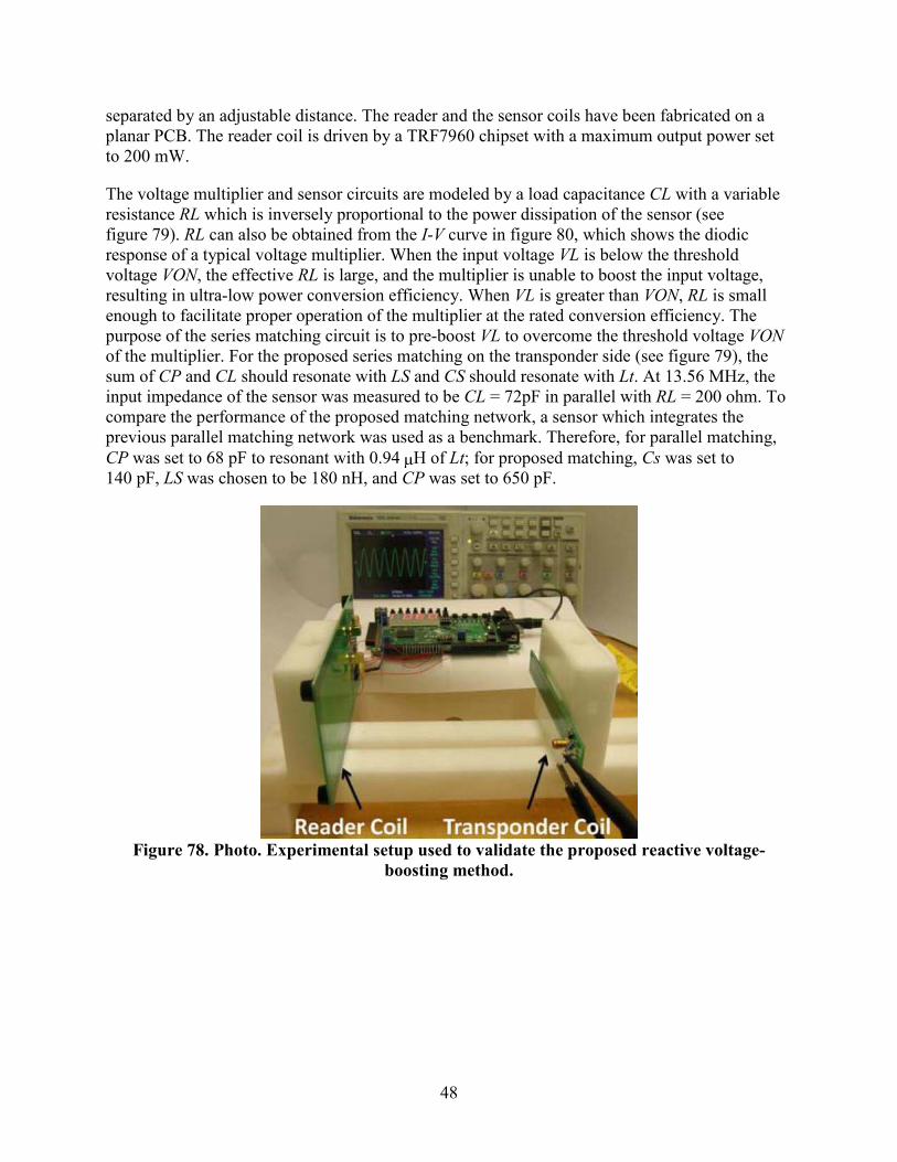
48
separated by an adjustable distance. The reader and the sensor coils have been fabricated on a planar PCB. The reader coil is driven by a TRF7960 chipset with a maximum output power set to 200 mW.
The voltage multiplier and sensor circuits are modeled by a load capacitance CL with a variable resistance RL which is inversely proportional to the power dissipation of the sensor (see figure 79). RL can also be obtained from the I-V curve in figure 80, which shows the diodic response of a typical voltage multiplier. When the input voltage VL is below the threshold voltage VON, the effective RL is large, and the multiplier is unable to boost the input voltage, resulting in ultra-low power conversion efficiency. When VL is greater than VON, RL is small enough to facilitate proper operation of the multiplier at the rated conversion efficiency. The purpose of the series matching circuit is to pre-boost VL to overcome the threshold voltage VON of the multiplier. For the proposed series matching on the transponder side (see figure 79), the sum of CP and CL should resonate with LS and CS should resonate with Lt. At 13.56 MHz, the input impedance of the sensor was measured to be CL = 72pF in parallel with RL = 200 ohm. To compare the performance of the proposed matching network, a sensor which integrates the previous parallel matching network was used as a benchmark. Therefore, for parallel matching, CP was set to 68 pF to resonant with 0.94 µ H of Lt; for proposed matching, Cs was set to 140 pF, LS was chosen to be 180 nH, and CP was set to 650 pF.
Figure 78. Photo. Experimental setup used to validate the proposed reactive voltage-
boosting method.
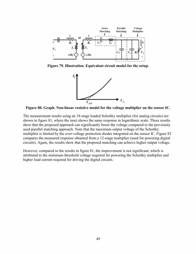
49
Figure 79. Illustration. Equivalent circuit model for the setup.
Figure 80. Graph. Non-linear resistive model for the voltage multiplier on the sensor IC.
The measurement results using an 18-stage loaded Schottky multiplier (for analog circuits) are shown in figure 81, where the inset shows the same response in logarithmic scale. These results show that the proposed approach can significantly boost the voltage compared to the previously used parallel matching approach. Note that the maximum output voltage of the Schottky multiplier is limited by the over-voltage protection diodes integrated on the sensor IC. Figure 82 compares the measured response obtained from a 12-stage multiplier (used for powering digital circuits). Again, the results show that the proposed matching can achieve higher output voltage.
However, compared to the results in figure 81, the improvement is not significant, which is attributed to the minimum threshold voltage required for powering the Schottky multiplier and higher load current required for driving the digital circuits.
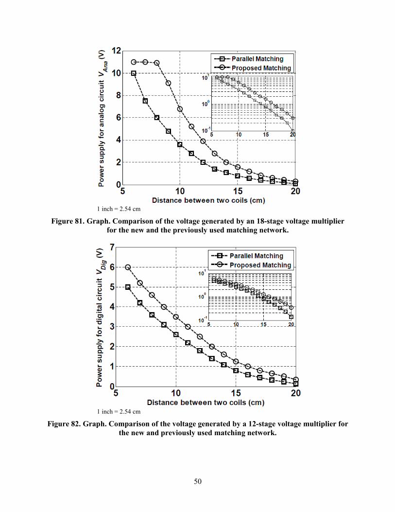
50
1 inch = 2.54 cm
Figure 81. Graph. Comparison of the voltage generated by an 18-stage voltage multiplier for the new and the previously used matching network.
1 inch = 2.54 cm
Figure 82. Graph. Comparison of the voltage generated by a 12-stage voltage multiplier for the new and previously used matching network.

51
3.5 CONCLUSION
This chapter describes the design and development of a novel RF communication module. The mixed mode module is specific for integration with the FG analog memories. The RF powering mode is dissociated from the computing and storage circuitry and is achieved by harvesting the RF signal. The salient modules of the RF module include the following:
• ADC for digitizing the stored usage statistics.
• Charge pumps for generating biases for erasing and remote initialization of the sensor.
• Encoding/decoding circuits for creating data packets with inherent clock/data recovery mechanisms.
• State machine for command and control of the IC.
• RF interface circuitry operating at 13.56 MHz for harvesting energy from the reader signal and for wireless transmission of the sensor data.
In addition, an external reader was designed and manufactured. The reader interfaces with an embedded antenna, which was also designed and manufactured in-house and fits the exact H-shape of the designed package. The embedded antenna is connected to the interface. Laboratory testing showed that the reading distance highly depends on the parasitic capacitances of the antennas (embedded antenna and external reader) as well as the parasitic capacitance at the sensors input. These capacitances are induced by the manufacturing process and cannot be predicted upfront. A calibration procedure and antennas resonance tuning is required.


53
CHAPTER 4. LABORATORY MECHANICAL TESTING OF THE PIEZOELECTRIC TRANSDUCER
The objective of the work described in this chapter is to test the survivability of the unprotected piezoelectric ceramic transducers embedded in asphalt under compaction conditions and in fresh mix concrete. The observed performance variations are used to determine the initial design parameters for the packaging system. Detailed design, manufacturing, and testing procedures for the package are described in chapter 5. Furthermore, the generation of electrical energy—a critical aspect for the performance of the entire system—is investigated under simulated stress/ strain conditions. Theoretical models of the piezoelectric power generation transducers are presented.
4.1 PIEZOELECTRIC TRANSDUCER DESIGN AND TESTING
Another component in the sensing system is the piezoelectric transducer. To evaluate the effect of temperature on the complete system, commercial lead zirconate titanate (PZT) piezoelectric transducers (CEB-35D26) were attached to AC specimens along with conventional linear variable differential transformers (LVDTs). Specimens were tested in the indirect tensile test configuration for different temperatures varying from 50 to 122 °F (10 to 50 °C). The test setup is shown in figure 83 through figure 85. A train of sinusoidal loading pulses was applied to each specimen. The magnitude of the pulses was set to increase by 225 lb (102.15 kg) for each 20 cycles, and the output of both the strain gauge and the piezo-transducer were monitored.
Figure 86 shows the correlation between the measured peak-to-peak strain and the observed peak-to peak output voltage of the piezoelectric disc for different temperatures. It can be seen that a linear correlation can be determined between the measured strain and the observed voltage. The fluctuations in the observed data are due to measurement errors in the strain and voltage. Testing the LVDTs at constant amplitude strain levels showed fluctuations of the results in the same order as errors observed in figure 86. This prompted the acquisition of a high-precision 50-Hz clip gauge (data sheet is attached in appendix A). The gauge was used for advanced calibration of the sensor (see chapter 6), thus allowing for a more reliable testing procedure.
From figure 86, it can be seen that the decreasing temperature increases the slope of the linear correlation. This phenomenon might be exploited to improve the measuring performance of the system. Alternative designs of the FG system could be studied with an envisioned objective of enhancing the sensor’s output by recording the temperature variations at the time of strain measurement and correlating it to different strain histograms output. The new design facilitates the interpretation algorithms and alleviates the need for correction algorithms. Several modified designs are still at the system-level simulations stage, and it is anticipated that such designs require many cycles of improvements and testing that might be beyond the scope of the current work.
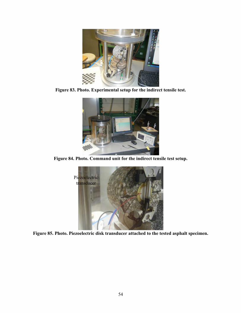
54
Figure 83. Photo. Experimental setup for the indirect tensile test.
Figure 84. Photo. Command unit for the indirect tensile test setup.
Figure 85. Photo. Piezoelectric disk transducer attached to the tested asphalt specimen.
Piezoelectric transducer
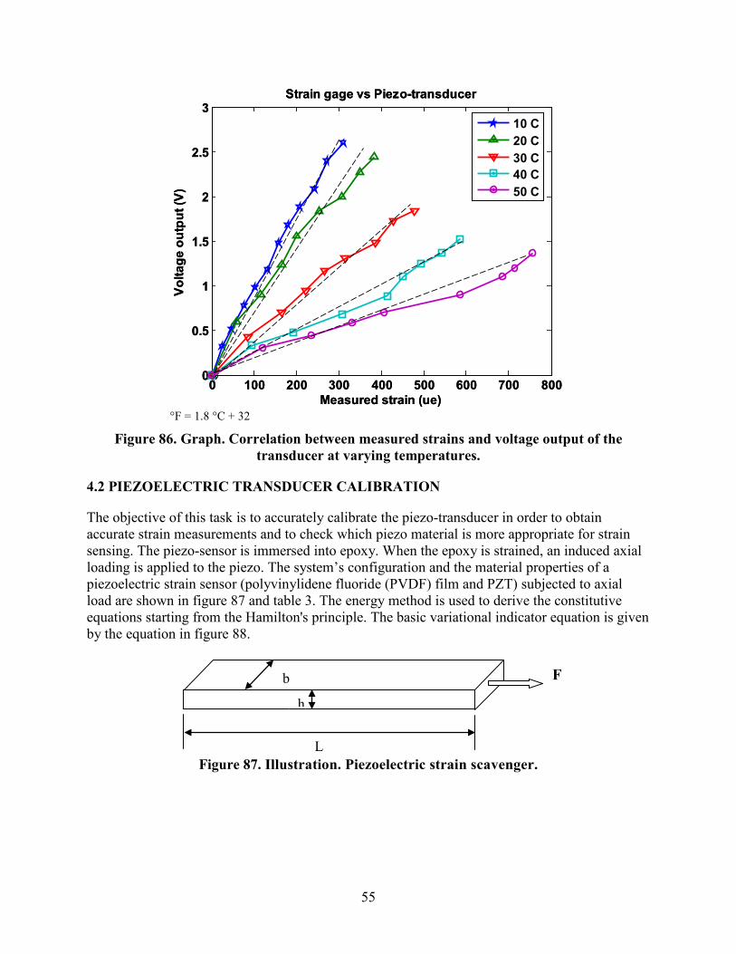
55
0 100 200 300 400 500 600 700 8000
0.5
1
1.5
2
2.5
3
Measured strain (ue)
Volta
ge o
utpu
t (V)
Strain gage vs Piezo-transducer
10 C20 C30 C40 C50 C
0 100 200 300 400 500 600 700 8000
0.5
1
1.5
2
2.5
3
Measured strain (ue)
Volta
ge o
utpu
t (V)
Strain gage vs Piezo-transducer
10 C20 C30 C40 C50 C
°F = 1.8 °C + 32
Figure 86. Graph. Correlation between measured strains and voltage output of the transducer at varying temperatures.
4.2 PIEZOELECTRIC TRANSDUCER CALIBRATION
The objective of this task is to accurately calibrate the piezo-transducer in order to obtain accurate strain measurements and to check which piezo material is more appropriate for strain sensing. The piezo-sensor is immersed into epoxy. When the epoxy is strained, an induced axial loading is applied to the piezo. The system’s configuration and the material properties of a piezoelectric strain sensor (polyvinylidene fluoride (PVDF) film and PZT) subjected to axial load are shown in figure 87 and table 3. The energy method is used to derive the constitutive equations starting from the Hamilton's principle. The basic variational indicator equation is given by the equation in figure 88.
h
b
L
F
Figure 87. Illustration. Piezoelectric strain scavenger.

56
Table 3. Piezoelectric sensor properties.
Sensor
Elastic Modulus
(psi)
Piezoelectric Constant d31
(mV)
Electrical Permittivity (Farad/m)
Beam Length (inches)
Beam Width (inches)
Thickness (inches)
PVDF 500,000 23e-12 7.7 ε 0 2.83 0.62 8×10⁻⁴ PZT 10.4×10⁶ 270e-12 3500 ε 0 1.57 0.4 0.02
ε = Vacuum permittivity.
� [δU + δW]t2
t1dt = 0
Figure 88. Equation. Varitional indicator.
Where U and W are the kinetic energy and the external work applied to the system, respectively, defined as follows:
U =1 2� STTdVs
Vs
+ 12
� STTdVpVp
+ 12
� ETDdVpVp
Figure 89. Equation. Kinetic energy.
W = uLF(t) Figure 90. Equation. External work.
Where:
u = Transverse displacement. ρ = Density. F = Applied load due to straining.
The subscripts p and s represent the PZT material and the metallic substrate, respectively. S, T, E, D, and V are the strain, the stress, the electric field, the electric displacement, and the material’s volume, respectively.
Incorporating the linear piezoelectricity equations into the potential energy function yields the following general potential form:
U =1 2� 𝑆𝑆𝑇𝑇𝐶𝐶𝑠𝑠SdVs
Vs
+ � ST𝑐𝑐𝐸𝐸SdVpVp
– � 𝑆𝑆𝑇𝑇𝑒𝑒𝑇𝑇EdVpVp
–� 𝐸𝐸𝑇𝑇𝑉𝑉𝑝𝑝
eSd𝑉𝑉𝑝𝑝 – � 𝐸𝐸𝑇𝑇𝜀𝜀𝑠𝑠𝑉𝑉𝑝𝑝
Ed𝑉𝑉𝑝𝑝
Figure 91. Equation. Potential energy.
Where:
c = Modulus of elasticity. ε = Dielectric constant. e = Coupling factor.
The superscripts, s and E, indicate that the parameter is estimated either at constant strain or constant electric field.

57
Taking the variation of the external work, the kinetic energy, and potential energy and substituting it into figure 54, the variational indicator is obtained.
2
1
0.
s p p
p p
Es s p p
V V V
sp p L
V V
t
t
S c SdV S c SdV S eEdV
EeSdV E EdVdt
u F
δ δ δ
δ δ ε δ
− − +
=+ + +
∫ ∫ ∫
∫ ∫∫
Figure 92. Equation. Variational indicator.
The longitudinal displacement and the electrical field are expressed in the shape mode and field coordinates as follows:
u (x,t) = Nu (x)r(t) Figure 93. Equation. Longitudinal displacement.
E (x,t) = ψ (y)v(t) Figure 94. Equation. Electric field.
Where ( )yψ defines the field over the thickness of the PZT.
Substituting figure 93 and figure 94 into the variational indicator leads to the two coupled equations in figure 95.
�Kr(t) – Θv(t) = F(t)
ΘTr(t) – Cpv(t) = q(t)�
Figure 95. Equation. Piezoelectric constitutive equation.
Where the stiffness matrices of the system can be written as follows:
K =� BuT
Vs
(x)csBu(x)dVs+ � BuT
Vp
(x)cpBu(x)dVp
Figure 96. Equation. Stiffness.
F is the applied load induced by the strain is expressed as follows:
F = SEepNu2 (L) Figure 97. Equation. Applied load induced by strain.
Where:
Sep = Elastic modulus. Eep = Strain of the epoxy.
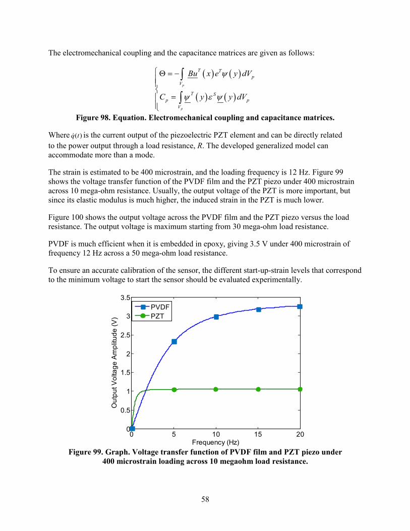
58
The electromechanical coupling and the capacitance matrices are given as follows:
( ) ( )
( ) ( )p
p
T Tp
V
T Sp p
V
Bu x e y dV
C y y dV
ψ
ψ ε ψ
Θ = −
=
∫
∫
Figure 98. Equation. Electromechanical coupling and capacitance matrices.
Where ( )q t is the current output of the piezoelectric PZT element and can be directly related to the power output through a load resistance, R. The developed generalized model can accommodate more than a mode.
The strain is estimated to be 400 microstrain, and the loading frequency is 12 Hz. Figure 99 shows the voltage transfer function of the PVDF film and the PZT piezo under 400 microstrain across 10 mega-ohm resistance. Usually, the output voltage of the PZT is more important, but since its elastic modulus is much higher, the induced strain in the PZT is much lower.
Figure 100 shows the output voltage across the PVDF film and the PZT piezo versus the load resistance. The output voltage is maximum starting from 30 mega-ohm load resistance.
PVDF is much efficient when it is embedded in epoxy, giving 3.5 V under 400 microstrain of frequency 12 Hz across a 50 mega-ohm load resistance.
To ensure an accurate calibration of the sensor, the different start-up-strain levels that correspond to the minimum voltage to start the sensor should be evaluated experimentally.
0 5 10 15 200
0.5
1
1.5
2
2.5
3
3.5
Frequency (Hz)
Out
put V
olta
ge A
mpl
itude
(V)
PVDFPZT
Figure 99. Graph. Voltage transfer function of PVDF film and PZT piezo under
400 microstrain loading across 10 megaohm load resistance.
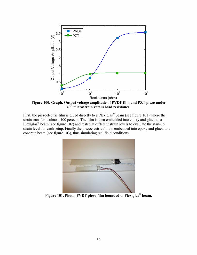
59
105 106 107 1080
0.5
1
1.5
2
2.5
3
3.5
4
Resistance (ohm)
Out
put V
olta
ge A
mpl
itude
(V)
PVDFPZT
Figure 100. Graph. Output voltage amplitude of PVDF film and PZT piezo under
400 microstrain versus load resistance.
First, the piezoelectric film is glued directly to a Plexiglas® beam (see figure 101) where the strain transfer is almost 100 percent. The film is then embedded into epoxy and glued to a Plexiglas® beam (see figure 102) and tested at different strain levels to evaluate the start-up strain level for each setup. Finally the piezoelectric film is embedded into epoxy and glued to a concrete beam (see figure 103), thus simulating real field conditions.
Figure 101. Photo. PVDF piezo film bounded to Plexiglas® beam.
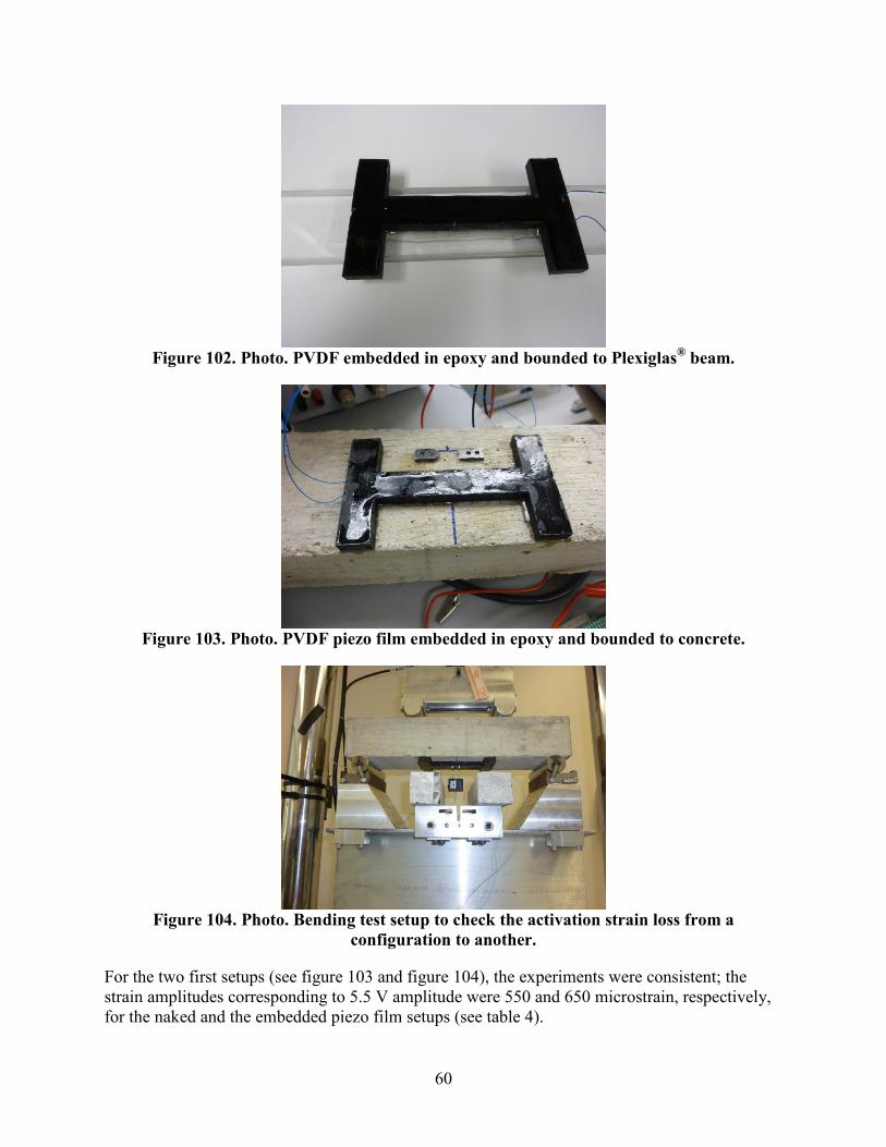
60
Figure 102. Photo. PVDF embedded in epoxy and bounded to Plexiglas® beam.
Figure 103. Photo. PVDF piezo film embedded in epoxy and bounded to concrete.
Figure 104. Photo. Bending test setup to check the activation strain loss from a
configuration to another.
For the two first setups (see figure 103 and figure 104), the experiments were consistent; the strain amplitudes corresponding to 5.5 V amplitude were 550 and 650 microstrain, respectively, for the naked and the embedded piezo film setups (see table 4).
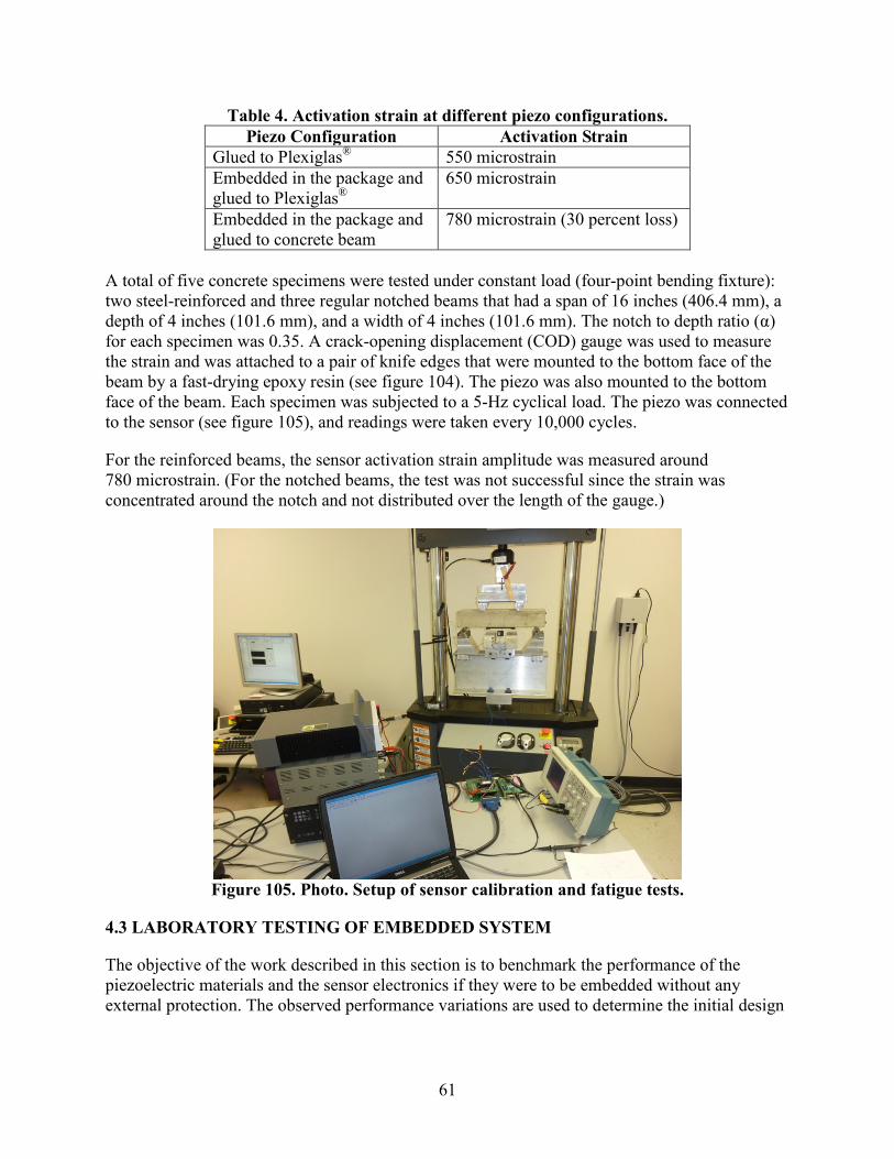
61
Table 4. Activation strain at different piezo configurations. Piezo Configuration Activation Strain
Glued to Plexiglas® 550 microstrain Embedded in the package and glued to Plexiglas®
650 microstrain
Embedded in the package and glued to concrete beam
780 microstrain (30 percent loss)
A total of five concrete specimens were tested under constant load (four-point bending fixture): two steel-reinforced and three regular notched beams that had a span of 16 inches (406.4 mm), a depth of 4 inches (101.6 mm), and a width of 4 inches (101.6 mm). The notch to depth ratio (α ) for each specimen was 0.35. A crack-opening displacement (COD) gauge was used to measure the strain and was attached to a pair of knife edges that were mounted to the bottom face of the beam by a fast-drying epoxy resin (see figure 104). The piezo was also mounted to the bottom face of the beam. Each specimen was subjected to a 5-Hz cyclical load. The piezo was connected to the sensor (see figure 105), and readings were taken every 10,000 cycles.
For the reinforced beams, the sensor activation strain amplitude was measured around 780 microstrain. (For the notched beams, the test was not successful since the strain was concentrated around the notch and not distributed over the length of the gauge.)
Figure 105. Photo. Setup of sensor calibration and fatigue tests.
4.3 LABORATORY TESTING OF EMBEDDED SYSTEM
The objective of the work described in this section is to benchmark the performance of the piezoelectric materials and the sensor electronics if they were to be embedded without any external protection. The observed performance variations are used to determine the initial design
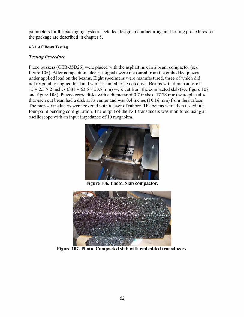
62
parameters for the packaging system. Detailed design, manufacturing, and testing procedures for the package are described in chapter 5.
4.3.1 AC Beam Testing
Testing Procedure
Piezo buzzers (CEB-35D26) were placed with the asphalt mix in a beam compactor (see figure 106). After compaction, electric signals were measured from the embedded piezos under applied load on the beams. Eight specimens were manufactured, three of which did not respond to applied load and were assumed to be defective. Beams with dimensions of 15 × 2.5 × 2 inches (381 × 63.5 × 50.8 mm) were cut from the compacted slab (see figure 107 and figure 108). Piezoelectric disks with a diameter of 0.7 inches (17.78 mm) were placed so that each cut beam had a disk at its center and was 0.4 inches (10.16 mm) from the surface. The piezo-transducers were covered with a layer of rubber. The beams were then tested in a four-point bending configuration. The output of the PZT transducers was monitored using an oscilloscope with an input impedance of 10 megaohm.
Figure 106. Photo. Slab compactor.
Figure 107. Photo. Compacted slab with embedded transducers.
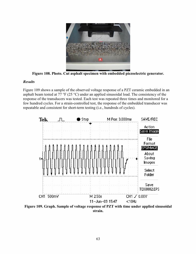
63
Figure 108. Photo. Cut asphalt specimen with embedded piezoelectric generator.
Results
Figure 109 shows a sample of the observed voltage response of a PZT ceramic embedded in an asphalt beam tested at 77 °F (25 °C) under an applied sinusoidal load. The consistency of the response of the transducers was tested. Each test was repeated three times and monitored for a few hundred cycles. For a strain-controlled test, the response of the embedded transducer was repeatable and consistent for short-term testing (i.e., hundreds of cycles).
Figure 109. Graph. Sample of voltage response of PZT with time under applied sinusoidal
strain.
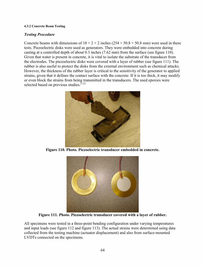
64
4.3.2 Concrete Beam Testing
Testing Procedure
Concrete beams with dimensions of 10 × 2 × 2 inches (254 × 50.8 × 50.8 mm) were used in these tests. Piezoelectric disks were used as generators. They were embedded into concrete during casting at a controlled depth of about 0.3 inches (7.62 mm) from the surface (see figure 110). Given that water is present in concrete, it is vital to isolate the substrate of the transducer from the electrodes. The piezoelectric disks were covered with a layer of rubber (see figure 111). The rubber is also useful to protect the disks from the external environment such as chemical attacks. However, the thickness of the rubber layer is critical to the sensitivity of the generator to applied strains, given that it defines the contact surface with the concrete. If it is too thick, it may modify or even block the strains from being transmitted in the transducers. The used epoxies were selected based on previous studies.(1,2)
Figure 110. Photo. Piezoelectric transducer embedded in concrete.
Figure 111. Photo. Piezoelectric transducer covered with a layer of rubber.
All specimens were tested in a three-point bending configuration under varying temperatures and input loads (see figure 112 and figure 113). The actual strains were determined using data collected from the testing machine (actuator displacement) and also from surface-mounted LVDTs connected on the specimens.
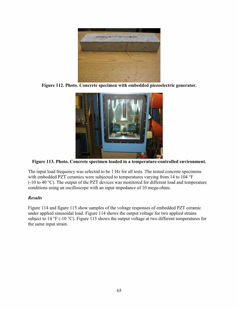
65
Figure 112. Photo. Concrete specimen with embedded piezoelectric generator.
Figure 113. Photo. Concrete specimen loaded in a temperature-controlled environment.
The input load frequency was selected to be 1 Hz for all tests. The tested concrete specimens with embedded PZT ceramics were subjected to temperatures varying from 14 to 104 °F (-10 to 40 °C). The output of the PZT devices was monitored for different load and temperature conditions using an oscilloscope with an input impedance of 10 mega-ohms.
Results
Figure 114 and figure 115 show samples of the voltage responses of embedded PZT ceramic under applied sinusoidal load. Figure 114 shows the output voltage for two applied strains subject to 14 °F (-10 °C). Figure 115 shows the output voltage at two different temperatures for the same input strain.
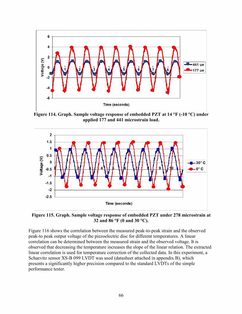
66
21 43 65 87
Figure 114. Graph. Sample voltage response of embedded PZT at 14 °F (-10 °C) under
applied 177 and 441 microstrain load.
Figure 115. Graph. Sample voltage response of embedded PZT under 278 microstrain at
32 and 86 °F (0 and 30 °C).
Figure 116 shows the correlation between the measured peak-to-peak strain and the observed peak-to peak output voltage of the piezoelectric disc for different temperatures. A linear correlation can be determined between the measured strain and the observed voltage. It is observed that decreasing the temperature increases the slope of the linear relation. The extracted linear correlation is used for temperature correction of the collected data. In this experiment, a Schaevitz sensor XS-B 099 LVDT was used (datasheet attached in appendix B), which presents a significantly higher precision compared to the standard LVDTs of the simple performance tester.
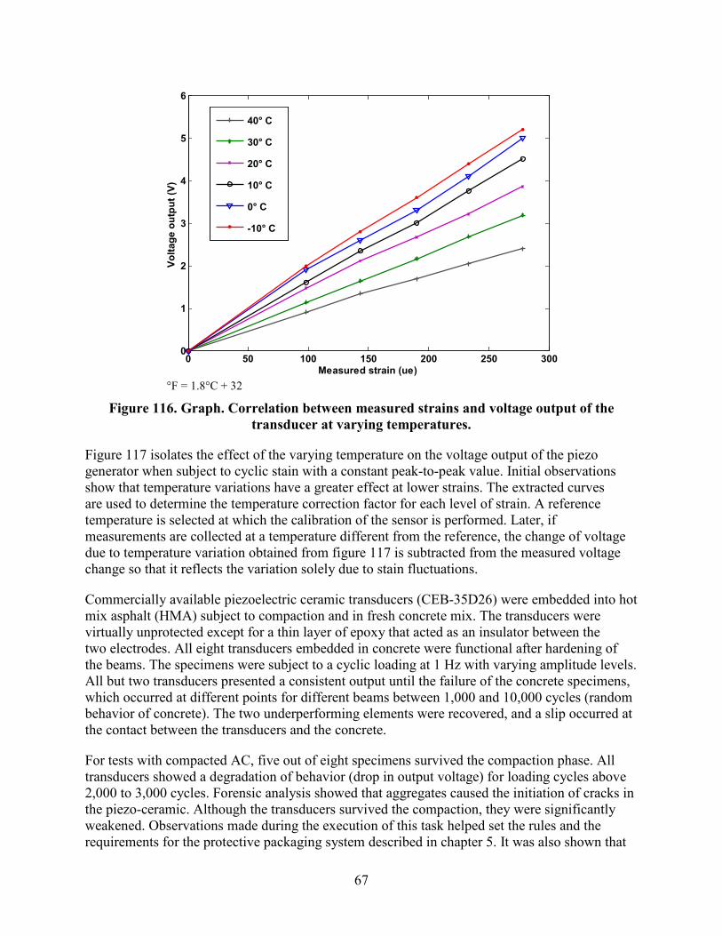
67
0 50 100 150 200 250 3000
1
2
3
4
5
6
Measured strain (ue)
Volta
ge o
utpu
t (V)
40° C
30° C
20° C
10° C
0° C
-10° C
°F = 1.8°C + 32
Figure 116. Graph. Correlation between measured strains and voltage output of the transducer at varying temperatures.
Figure 117 isolates the effect of the varying temperature on the voltage output of the piezo generator when subject to cyclic stain with a constant peak-to-peak value. Initial observations show that temperature variations have a greater effect at lower strains. The extracted curves are used to determine the temperature correction factor for each level of strain. A reference temperature is selected at which the calibration of the sensor is performed. Later, if measurements are collected at a temperature different from the reference, the change of voltage due to temperature variation obtained from figure 117 is subtracted from the measured voltage change so that it reflects the variation solely due to stain fluctuations.
Commercially available piezoelectric ceramic transducers (CEB-35D26) were embedded into hot mix asphalt (HMA) subject to compaction and in fresh concrete mix. The transducers were virtually unprotected except for a thin layer of epoxy that acted as an insulator between the two electrodes. All eight transducers embedded in concrete were functional after hardening of the beams. The specimens were subject to a cyclic loading at 1 Hz with varying amplitude levels. All but two transducers presented a consistent output until the failure of the concrete specimens, which occurred at different points for different beams between 1,000 and 10,000 cycles (random behavior of concrete). The two underperforming elements were recovered, and a slip occurred at the contact between the transducers and the concrete.
For tests with compacted AC, five out of eight specimens survived the compaction phase. All transducers showed a degradation of behavior (drop in output voltage) for loading cycles above 2,000 to 3,000 cycles. Forensic analysis showed that aggregates caused the initiation of cracks in the piezo-ceramic. Although the transducers survived the compaction, they were significantly weakened. Observations made during the execution of this task helped set the rules and the requirements for the protective packaging system described in chapter 5. It was also shown that
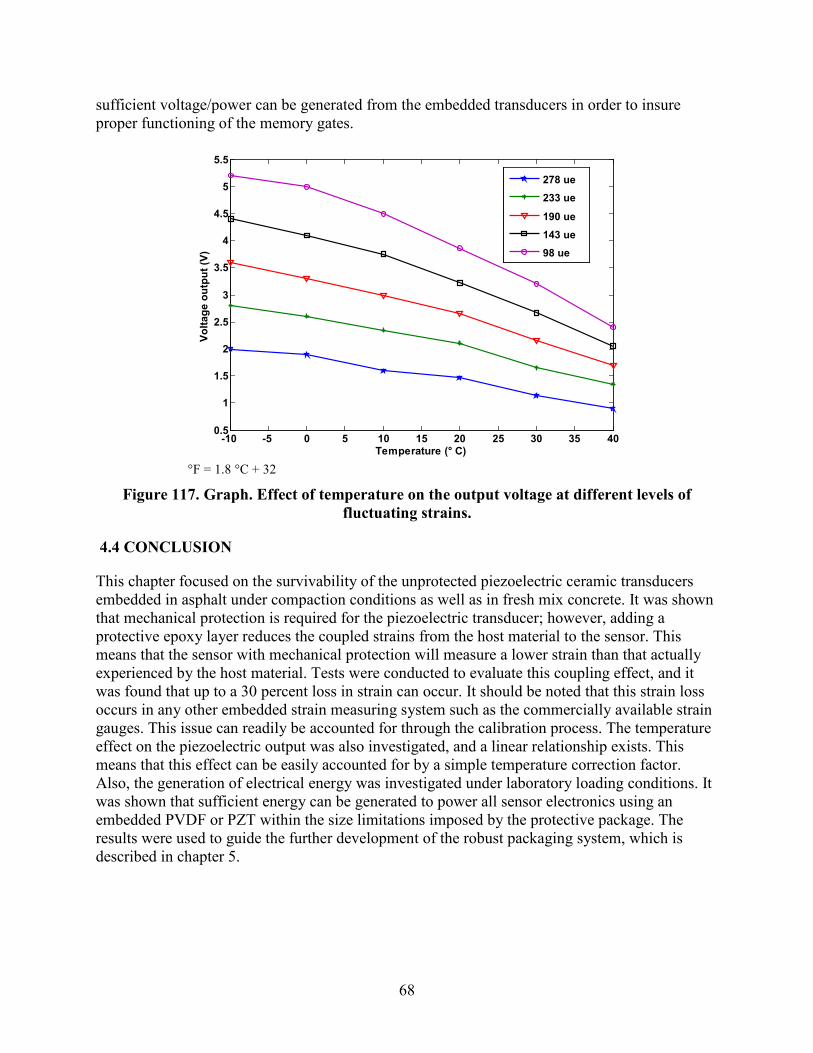
68
sufficient voltage/power can be generated from the embedded transducers in order to insure proper functioning of the memory gates.
-10 -5 0 5 10 15 20 25 30 35 400.5
1
1.5
2
2.5
3
3.5
4
4.5
5
5.5
Temperature (° C)
Volta
ge o
utpu
t (V)
278 ue233 ue
190 ue143 ue98 ue
°F = 1.8 °C + 32
Figure 117. Graph. Effect of temperature on the output voltage at different levels of fluctuating strains.
4.4 CONCLUSION
This chapter focused on the survivability of the unprotected piezoelectric ceramic transducers embedded in asphalt under compaction conditions as well as in fresh mix concrete. It was shown that mechanical protection is required for the piezoelectric transducer; however, adding a protective epoxy layer reduces the coupled strains from the host material to the sensor. This means that the sensor with mechanical protection will measure a lower strain than that actually experienced by the host material. Tests were conducted to evaluate this coupling effect, and it was found that up to a 30 percent loss in strain can occur. It should be noted that this strain loss occurs in any other embedded strain measuring system such as the commercially available strain gauges. This issue can readily be accounted for through the calibration process. The temperature effect on the piezoelectric output was also investigated, and a linear relationship exists. This means that this effect can be easily accounted for by a simple temperature correction factor. Also, the generation of electrical energy was investigated under laboratory loading conditions. It was shown that sufficient energy can be generated to power all sensor electronics using an embedded PVDF or PZT within the size limitations imposed by the protective package. The results were used to guide the further development of the robust packaging system, which is described in chapter 5.

69
CHAPTER 5. DESIGN OF ROBUST PACKAGING SYSTEM AND INITIAL FIELD TRIALS
This chapter describes the designing and testing of an implementable version of the sensing module. The shape, size, and the conformity with the current installation procedures were important factors in the design.
5.1 CURRENT STATE OF THE PARCTICE FOR STRAIN GAUGE INSTALLATION TECHNIQUES
Embedded strain gauges made specifically for AC have been widely used by several research programs. The used sensing principle is based on mechanical indicators such as an extensometer, resistive wires, and foil gauges. To ensure a good contact, most of the recently developed and marketed gauges are H-shaped (see figure 118 and figure 119). It was decided that the package designed for the sensor should have a similar shape and could be installed using existing installation procedures that are accepted by State transportation departments and will not constitute a major disruption to current practices.
Figure 118. Photo. Example of commercially available asphalt strain gauge.
Figure 119. Photo. Second example of commercially available asphalt strain gauge.
Many past projects dealt with the installation of monitoring gauges in both asphalt and concrete pavements. This section describes the used installation procedure based on the work by

70
Hornyak et al. from the Transportation Research Center at Marquette University and a report prepared for the California Department of Transportation (Caltrans) by Roesler et al.(3,4) The locations of the gauges were identified and marked. A pre-mixed matrix of sand and binder was reheated and placed in a 0.5-inch (12.7-mm)-thick patch on an open-graded base layer at the location of each sensor. These patches served as the base pad for the asphalt strain gauges (ASGs). The ASGs were then placed on their respective base pads, and the leads were organized and buried into the open-graded base layer (see figure 120 and figure 121). A cable armor installed on the exposed length of the leads served as protection for the wiring from puncturing from the aggregates during paving. The ASGs were placed so that the leads exiting the protected portion of the gauge did so against the direction of paving; otherwise, forces and motions generated by the paving equipment may have a tendency to pull the sensor leads away from the strain gauge, destroying the gauge. Strain relief was provided multiple times. Shortly before the paving, asphalt material from the paver hopper was screened off on the 3/8-inch (9.53-mm) sieve and a roughly 1 inch (25.4 mm) layer was placed on the gauges. The material was compacted by mild compaction force using a hand tamper. A layer of unscreened asphalt (about 2 inches (50.8 mm) thick) was placed on top of the gauge arrays and compacted using a gas-powered plate tamper (see figure 122 and figure 123). After this was complete, the paver passed over the strain gauges. The wireless nature of the developed system reduces the required preparation time before paving.
Off-the-shelf dynamic strain monitoring gauges were used in the Caltrans project.(4) The used installation techniques could be considered representative of methods currently used by State transportation departments. Initially, shallow trenches were dug in the aggregate base, and polyvinyl chloride (PVC) pipes were laid in the trenches so that wires running from each instrument could be threaded through the PVC pipe system to the shoulder of the pavement and connected to the online data acquisition (see figure 124 and figure 125). The channels and pipe system were then backfilled with the aggregate base. For the cement-treated base, a saw was used to cut shallow grooves in which to run the gauge lead wires (see figure 124 and figure 125). These steps are skipped when installing a newly developed sensor. After the wires were placed, fast-setting cement mixed with sand was used to backfill the channels. All strain gauges were placed on the base material with small steel frames (see figure 126). Each instrument was attached to its steel frame using a plastic zip tie. Each instrument was attached firmly enough so that it would not become dislodged when the concrete was placed but also in such a manner that the fasteners would not restrict gauge movement once the concrete had set.
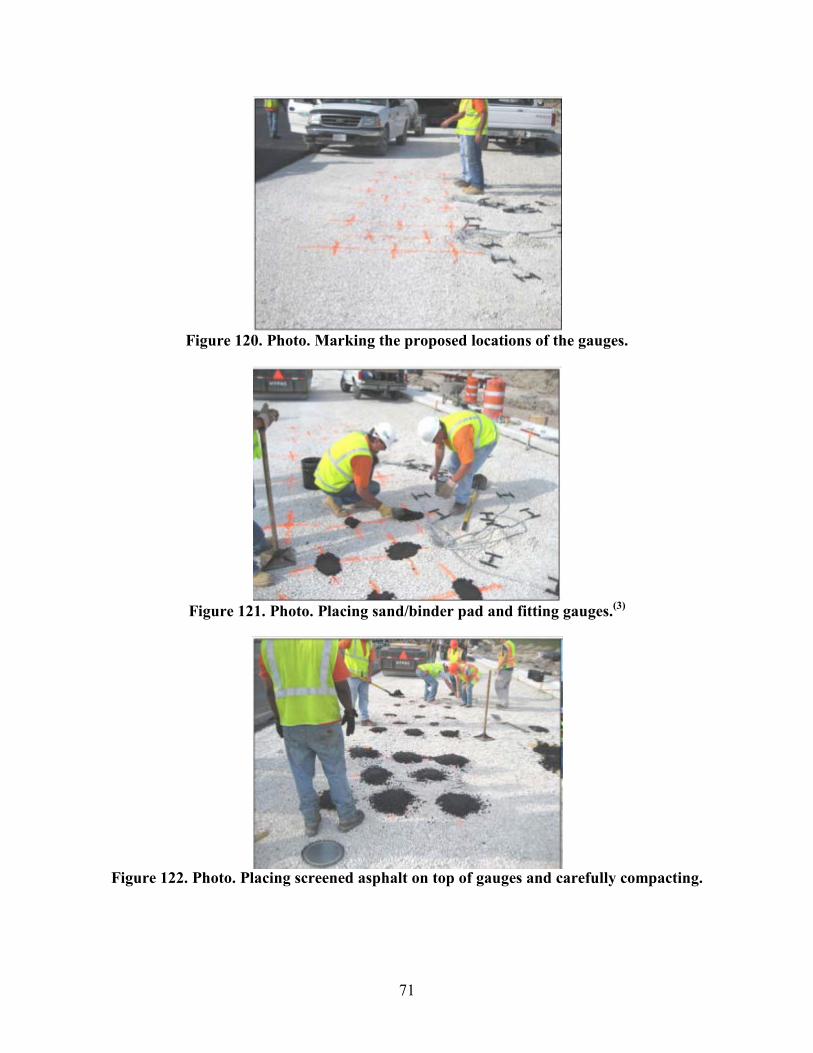
71
Figure 120. Photo. Marking the proposed locations of the gauges.
Figure 121. Photo. Placing sand/binder pad and fitting gauges.(3)
Figure 122. Photo. Placing screened asphalt on top of gauges and carefully compacting.

72
Figure 123. Photo. Compacting the unscreened asphalt over the gauge arrays.
Figure 124. Photo. Laying instrument wiring and piping in aggregate base.
Figure 125. Photo. Cutting grooves in cement-treated base for instrument leads.(4)
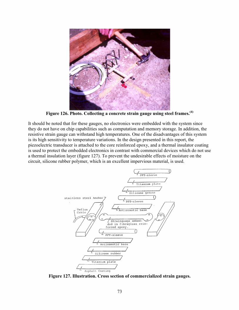
73
Figure 126. Photo. Collecting a concrete strain gauge using steel frames.(4)
It should be noted that for these gauges, no electronics were embedded with the system since they do not have on chip capabilities such as computation and memory storage. In addition, the resistive strain gauge can withstand high temperatures. One of the disadvantages of this system is its high sensitivity to temperature variations. In the design presented in this report, the piezoelectric transducer is attached to the core reinforced epoxy, and a thermal insulator coating is used to protect the embedded electronics in contrast with commercial devices which do not use a thermal insulation layer (figure 127). To prevent the undesirable effects of moisture on the circuit, silicone rubber polymer, which is an excellent impervious material, is used.
Figure 127. Illustration. Cross section of commercialized strain gauges.

74
In order to not disrupt the stress field in the pavement, the system’s stiffness must be close to that of the pavement. A low stiffness is desirable, but the device must be able to survive the stresses imposed during paving. Most of the systems are designed to approach the stiffness of asphalt at 77 °F and 320,000 psi (25 °C and 2,204,800 kPa). The main frame of the package is made of epoxy on which the sensor and the piezoelectric are attached. The layers used for thermal and chemical insulation have a very low stiffness compared to the main frame epoxy. The choice of the epoxy is based on several parameters such as the thermal conductivity and the electric conductivity. Two types of epoxy were identified—Conathane® TU-981 and Araldite® GY-6010. Both types have a tensile modulus close to 300,000 psi (2,067,000 kPa) and high tensile and flexural strengths above 4,000 psi (27,560 kPa). Both are good electric insulators, but the Araldite® GY-6010 has an upper thermal resistivity.
5.2 SYSTEM DESIGN
5.2.1 Thermal Insulation
According to the results shown in Timm et al., the typical mix temperature in a paving project decreases from around 302 °F (150 °C) to around 158 °F (70 °C) in about 2 h and then oscillates between 158 and 212 °F (70 and 100 °C) as lifts are applied.(5) Thus, the circuit needs to be protected. From a simple finite element simulation in which the external temperature is assumed to be constant all the time at 302 °F (150 °C) (conservative condition), it was concluded that the conductivity of a 0.4-inch (10.16-mm) isolating material layer should be less than 0.554 inch hr-1ft-2 °F-1 (0.08 W/mK). Polyurethane foam was identified as a viable candidate for thermal protection. Its thermal conductivity is lower than 0.346 inch hr-1ft-2 °F-1 (0.05 W/mK). Furthermore, it has a high abrasion resistance and impact strength. The selected foam was tested in a high-temperature environment where three thermocouples were placed inside an environmental chamber with a controlled temperature increasing gradually from 86 to 230 °F (30 to 110 °C) and then maintained at that level for 60 min. The first thermocouple was placed with no protection, while the second and third thermocouples had coats of 0.08 and 0.3 inches (2.03 and 7.62 mm), respectively. A sample is shown in figure 128. Figure 129 shows the variation of temperature for different sensors. From the figure, it is observed that a polyurethane layer significantly decreases the observed temperature.
Figure 128. Photo. Thermocouple covered with a layer of polyurethane foam.
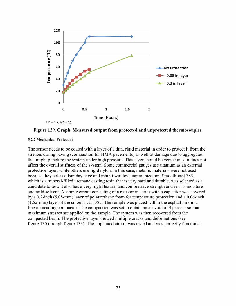
75
0.08 in layer
0.3 in layer
°F = 1.8 °C + 32
Figure 129. Graph. Measured output from protected and unprotected thermocouples.
5.2.2 Mechanical Protection
The sensor needs to be coated with a layer of a thin, rigid material in order to protect it from the stresses during paving (compaction for HMA pavements) as well as damage due to aggregates that might puncture the system under high pressure. This layer should be very thin so it does not affect the overall stiffness of the system. Some commercial gauges use titanium as an external protective layer, while others use rigid nylon. In this case, metallic materials were not used because they act as a Faraday cage and inhibit wireless communication. Smooth-cast 385, which is a mineral-filled urethane casting resin that is very hard and durable, was selected as a candidate to test. It also has a very high flexural and compressive strength and resists moisture and mild solvent. A simple circuit consisting of a resistor in series with a capacitor was covered by a 0.2-inch (5.08-mm) layer of polyurethane foam for temperature protection and a 0.06-inch (1.52-mm) layer of the smooth-cast 385. The sample was placed within the asphalt mix in a linear kneading compactor. The compaction was set to obtain an air void of 4 percent so that maximum stresses are applied on the sample. The system was then recovered from the compacted beam. The protective layer showed multiple cracks and deformations (see figure 130 through figure 133). The implanted circuit was tested and was perfectly functional.
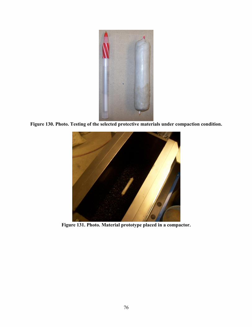
76
Figure 130. Photo. Testing of the selected protective materials under compaction condition.
Figure 131. Photo. Material prototype placed in a compactor.
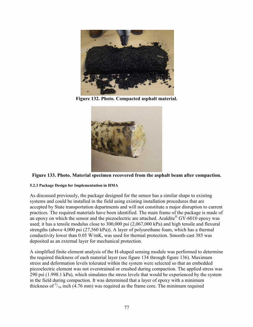
77
Figure 132. Photo. Compacted asphalt material.
Figure 133. Photo. Material specimen recovered from the asphalt beam after compaction.
5.2.3 Package Design for Implementation in HMA
As discussed previously, the package designed for the sensor has a similar shape to existing systems and could be installed in the field using existing installation procedures that are accepted by State transportation departments and will not constitute a major disruption to current practices. The required materials have been identified. The main frame of the package is made of an epoxy on which the sensor and the piezoelectric are attached. Araldite® GY-6010 epoxy was used; it has a tensile modulus close to 300,000 psi (2,067,000 kPa) and high tensile and flexural strengths (above 4,000 psi (27,560 kPa)). A layer of polyurethane foam, which has a thermal conductivity lower than 0.05 W/mK, was used for thermal protection. Smooth-cast 385 was deposited as an external layer for mechanical protection.
A simplified finite element analysis of the H-shaped sensing module was performed to determine the required thickness of each material layer (see figure 134 through figure 136). Maximum stress and deformation levels tolerated within the system were selected so that an embedded piezoelectric element was not overstrained or crushed during compaction. The applied stress was 290 psi (1.998.1 kPa), which simulates the stress levels that would be experienced by the system in the field during compaction. It was determined that a layer of epoxy with a minimum thickness of 3/16 inch (4.76 mm) was required as the frame core. The minimum required
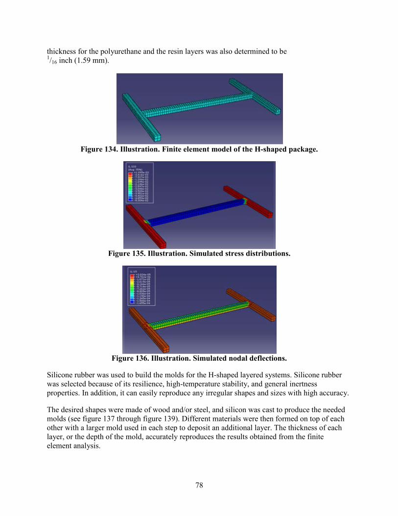
78
thickness for the polyurethane and the resin layers was also determined to be 1/16 inch (1.59 mm).
Figure 134. Illustration. Finite element model of the H-shaped package.
Figure 135. Illustration. Simulated stress distributions.
Figure 136. Illustration. Simulated nodal deflections.
Silicone rubber was used to build the molds for the H-shaped layered systems. Silicone rubber was selected because of its resilience, high-temperature stability, and general inertness properties. In addition, it can easily reproduce any irregular shapes and sizes with high accuracy.
The desired shapes were made of wood and/or steel, and silicon was cast to produce the needed molds (see figure 137 through figure 139). Different materials were then formed on top of each other with a larger mold used in each step to deposit an additional layer. The thickness of each layer, or the depth of the mold, accurately reproduces the results obtained from the finite element analysis.
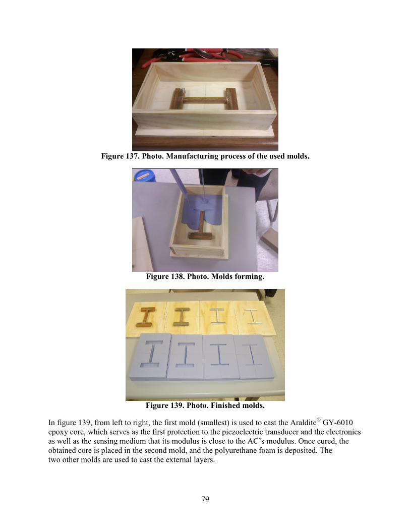
79
Figure 137. Photo. Manufacturing process of the used molds.
Figure 138. Photo. Molds forming.
Figure 139. Photo. Finished molds.
In figure 139, from left to right, the first mold (smallest) is used to cast the Araldite® GY-6010 epoxy core, which serves as the first protection to the piezoelectric transducer and the electronics as well as the sensing medium that its modulus is close to the AC’s modulus. Once cured, the obtained core is placed in the second mold, and the polyurethane foam is deposited. The two other molds are used to cast the external layers.
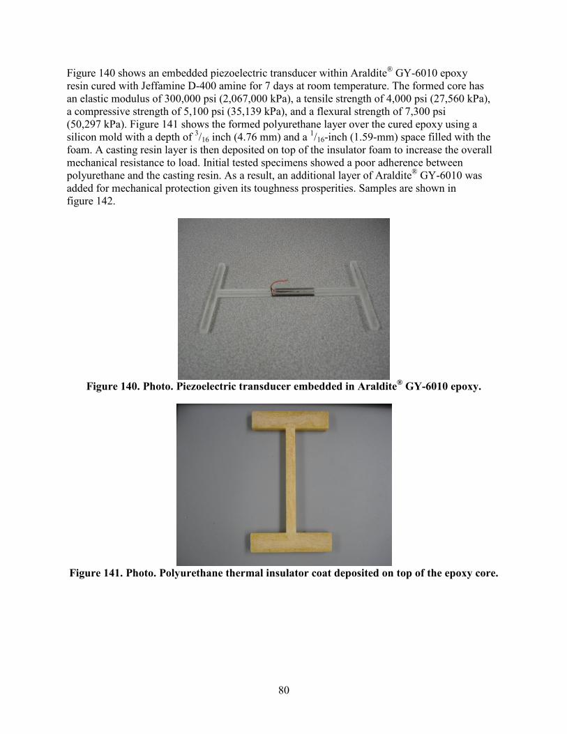
80
Figure 140 shows an embedded piezoelectric transducer within Araldite® GY-6010 epoxy resin cured with Jeffamine D-400 amine for 7 days at room temperature. The formed core has an elastic modulus of 300,000 psi (2,067,000 kPa), a tensile strength of 4,000 psi (27,560 kPa), a compressive strength of 5,100 psi (35,139 kPa), and a flexural strength of 7,300 psi (50,297 kPa). Figure 141 shows the formed polyurethane layer over the cured epoxy using a silicon mold with a depth of 3/16 inch (4.76 mm) and a 1/16-inch (1.59-mm) space filled with the foam. A casting resin layer is then deposited on top of the insulator foam to increase the overall mechanical resistance to load. Initial tested specimens showed a poor adherence between polyurethane and the casting resin. As a result, an additional layer of Araldite® GY-6010 was added for mechanical protection given its toughness prosperities. Samples are shown in figure 142.
Figure 140. Photo. Piezoelectric transducer embedded in Araldite® GY-6010 epoxy.
Figure 141. Photo. Polyurethane thermal insulator coat deposited on top of the epoxy core.
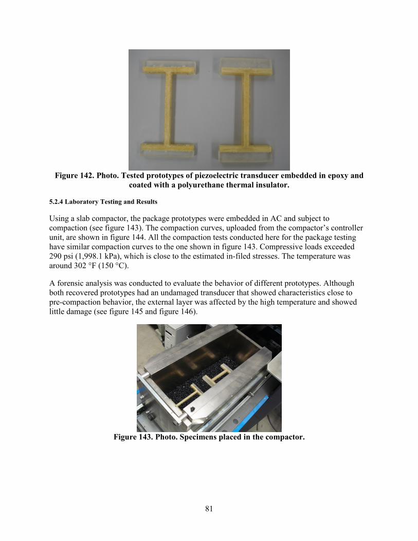
81
Figure 142. Photo. Tested prototypes of piezoelectric transducer embedded in epoxy and
coated with a polyurethane thermal insulator.
5.2.4 Laboratory Testing and Results
Using a slab compactor, the package prototypes were embedded in AC and subject to compaction (see figure 143). The compaction curves, uploaded from the compactor’s controller unit, are shown in figure 144. All the compaction tests conducted here for the package testing have similar compaction curves to the one shown in figure 143. Compressive loads exceeded 290 psi (1,998.1 kPa), which is close to the estimated in-filed stresses. The temperature was around 302 °F (150 °C).
A forensic analysis was conducted to evaluate the behavior of different prototypes. Although both recovered prototypes had an undamaged transducer that showed characteristics close to pre-compaction behavior, the external layer was affected by the high temperature and showed little damage (see figure 145 and figure 146).
Figure 143. Photo. Specimens placed in the compactor.
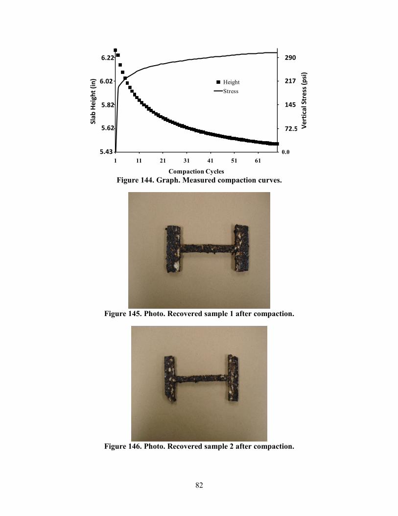
82
0.0
500.0
1000.0
1500.0
2000.0
138
143
148
153
158
1 11 21 31 41 51 61
Vert
ical
Str
ess
(kPa
)
Slab
Hei
ght (
mm
)
Compaction Cycles
HeightStress
72.5
145
217
290
Vert
ical
Str
ess (
psi)
5.62
5.82
5.43
6.02
6.22
Slab
Hei
ght (
in)
Figure 144. Graph. Measured compaction curves.
Figure 145. Photo. Recovered sample 1 after compaction.
Figure 146. Photo. Recovered sample 2 after compaction.
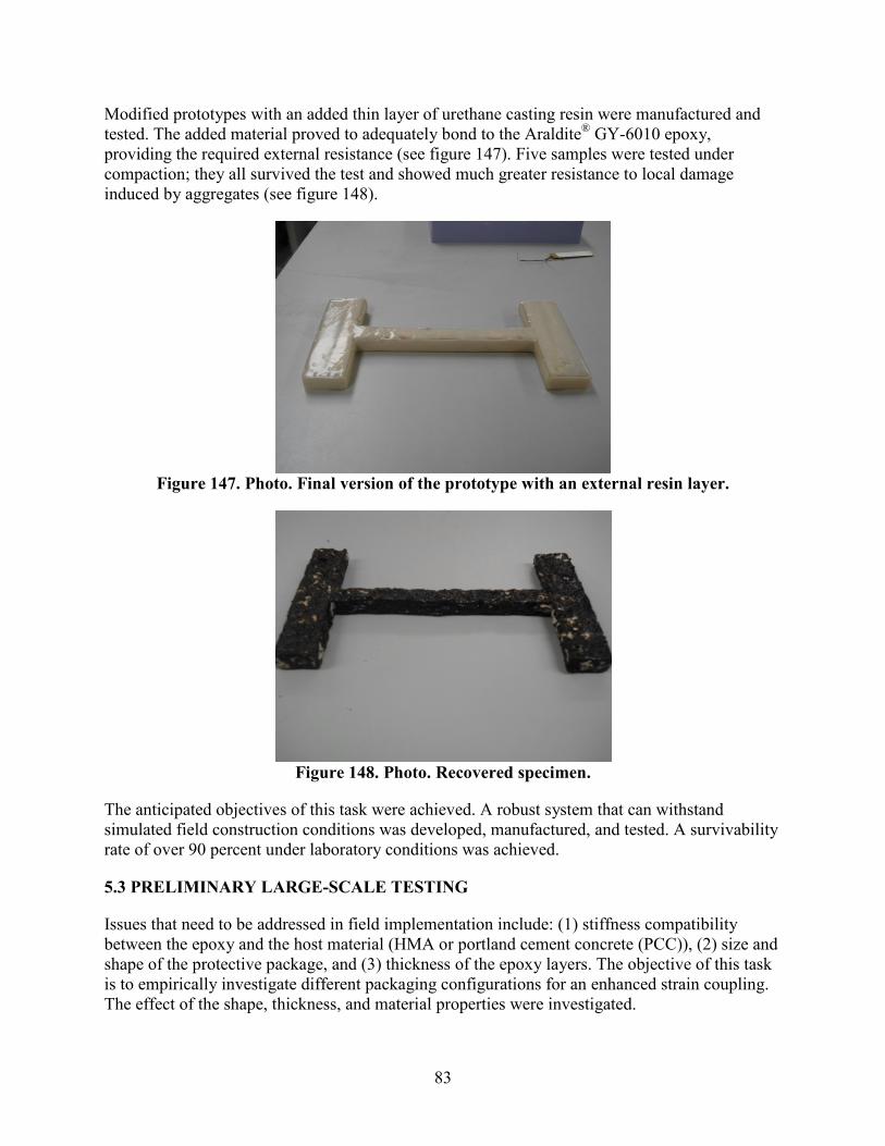
83
Modified prototypes with an added thin layer of urethane casting resin were manufactured and tested. The added material proved to adequately bond to the Araldite® GY-6010 epoxy, providing the required external resistance (see figure 147). Five samples were tested under compaction; they all survived the test and showed much greater resistance to local damage induced by aggregates (see figure 148).
Figure 147. Photo. Final version of the prototype with an external resin layer.
Figure 148. Photo. Recovered specimen.
The anticipated objectives of this task were achieved. A robust system that can withstand simulated field construction conditions was developed, manufactured, and tested. A survivability rate of over 90 percent under laboratory conditions was achieved.
5.3 PRELIMINARY LARGE-SCALE TESTING
Issues that need to be addressed in field implementation include: (1) stiffness compatibility between the epoxy and the host material (HMA or portland cement concrete (PCC)), (2) size and shape of the protective package, and (3) thickness of the epoxy layers. The objective of this task is to empirically investigate different packaging configurations for an enhanced strain coupling. The effect of the shape, thickness, and material properties were investigated.

84
Stiffness compatibility can be achieved using epoxy with a lower stiffness than the host material. Two different materials were used: Araldite® GY-6010 epoxy cured with Jeffamine D-400 and Conathane® TU-981.
Most of the commercialized strain gauges are H-shaped. The anchors are usually metallic to avoid damage in the corners due to stress concentration. However, for better structure integration and strain transfer, the modulus of those anchors should be the same or less than the modulus of the host material. Two different shapes were considered: regular H-shaped and bone-shaped (developed in the lab).
The third parameter to investigate is the gauge thickness. While increasing the thickness leads to higher survivability rates, it affects the structural integrity of the host material. Using very thin gauges is conceptually desirable for better strain compatibility between the gauge and the host material; however, they are more prone to breakage. Two different thicknesses were evaluated for the different shapes and materials: 1/4 and 3/8 inch (6.35 and 9.53 mm).
The strain gauges were tested at TFHRC’s ALF. The gauges were installed following the schematic shown in figure 149.
Center Line Wheel Path
Figure 149. Illustration. Layout of ASGs.
Simulations using the Viscoroute program were conducted to estimate the expected strains in the ALF test lane and compare with the strain measurements from the different gauge configurations. The pavement structural configuration and material properties were obtained from FHWA. The moduli of different layers were backcalculated using EVERCALC© at a pavement temperature of 78.8 °F (26 °C). Strain gauge responses were recorded at a temperature of 66.2 °F (19 °C) and a wheel load of 16,000 lb (7,264 kg). Figure 150 shows a typical computed longitudinal strain at the surface under a moving load. As the load approaches a fixed point in the pavement (where the gauge is), the strain increases in tension and then reverses from tension to compression then back to tension as the load moves away from it before dying out.
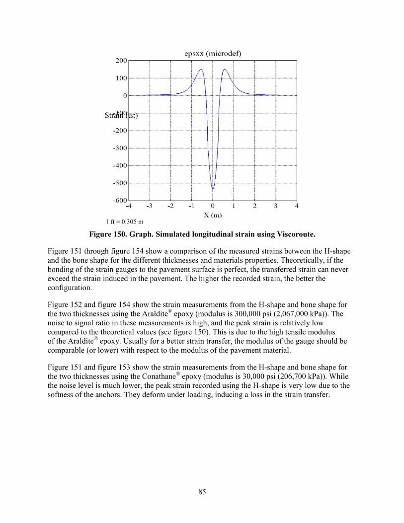
85
Strain (uε)
1 ft = 0.305 m
Figure 150. Graph. Simulated longitudinal strain using Viscoroute.
Figure 151 through figure 154 show a comparison of the measured strains between the H-shape and the bone shape for the different thicknesses and materials properties. Theoretically, if the bonding of the strain gauges to the pavement surface is perfect, the transferred strain can never exceed the strain induced in the pavement. The higher the recorded strain, the better the configuration.
Figure 152 and figure 154 show the strain measurements from the H-shape and bone shape for the two thicknesses using the Araldite® epoxy (modulus is 300,000 psi (2,067,000 kPa)). The noise to signal ratio in these measurements is high, and the peak strain is relatively low compared to the theoretical values (see figure 150). This is due to the high tensile modulus of the Araldite® epoxy. Usually for a better strain transfer, the modulus of the gauge should be comparable (or lower) with respect to the modulus of the pavement material.
Figure 151 and figure 153 show the strain measurements from the H-shape and bone shape for the two thicknesses using the Conathane® epoxy (modulus is 30,000 psi (206,700 kPa)). While the noise level is much lower, the peak strain recorded using the H-shape is very low due to the softness of the anchors. They deform under loading, inducing a loss in the strain transfer.
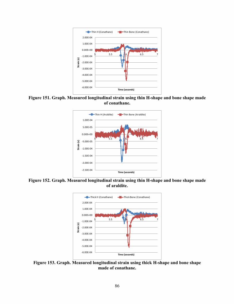
86
-6.00E-04
-5.00E-04
-4.00E-04
-3.00E-04
-2.00E-04
-1.00E-04
0.00E+00
1.00E-04
2.00E-04
5 5.5 6 6.5 7
Stra
in (ε
)
Time (seconds)
Thin H (Conathane) Thin Bone (Conathane)
Figure 151. Graph. Measured longitudinal strain using thin H-shape and bone shape made
of conathane.
-2.50E-04
-2.00E-04
-1.50E-04
-1.00E-04
-5.00E-05
0.00E+00
5.00E-05
1.00E-04
5 5.5 6 6.5 7
Stra
in (ε
)
Time (seconds)
Thin H (Araldite) Thin Bone (Araldite)
Figure 152. Graph. Measured longitudinal strain using thin H-shape and bone shape made
of araldite.
-6.00E-04
-5.00E-04
-4.00E-04
-3.00E-04
-2.00E-04
-1.00E-04
0.00E+00
1.00E-04
2.00E-04
5 5.5 6 6.5 7
Stra
in (ε
)
Time (seconds)
Thick H (Conathane) Thick Bone (Conathane)
Figure 153. Graph. Measured longitudinal strain using thick H-shape and bone shape
made of conathane.
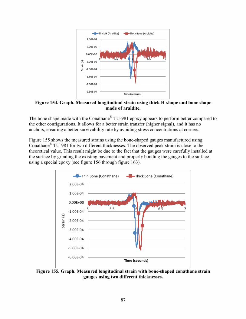
87
-2.50E-04
-2.00E-04
-1.50E-04
-1.00E-04
-5.00E-05
0.00E+00
5.00E-05
1.00E-04
5 5.5 6 6.5 7
Stra
in (ε
)
Time (seconds)
Thick H (Araldite) Thick Bone (Araldite)
Figure 154. Graph. Measured longitudinal strain using thick H-shape and bone shape
made of araldite.
The bone shape made with the Conathane® TU-981 epoxy appears to perform better compared to the other configurations. It allows for a better strain transfer (higher signal), and it has no anchors, ensuring a better survivability rate by avoiding stress concentrations at corners.
Figure 155 shows the measured strains using the bone-shaped gauges manufactured using Conathane® TU-981 for two different thicknesses. The observed peak strain is close to the theoretical value. This result might be due to the fact that the gauges were carefully installed at the surface by grinding the existing pavement and properly bonding the gauges to the surface using a special epoxy (see figure 156 through figure 163).
-6.00E-04
-5.00E-04
-4.00E-04
-3.00E-04
-2.00E-04
-1.00E-04
0.00E+00
1.00E-04
2.00E-04
5 5.5 6 6.5 7
Stra
in (ε
)
Time (seconds)
Thin Bone (Conathane) Thick Bone (Conathane)
Figure 155. Graph. Measured longitudinal strain with bone-shaped conathane strain
gauges using two different thicknesses.
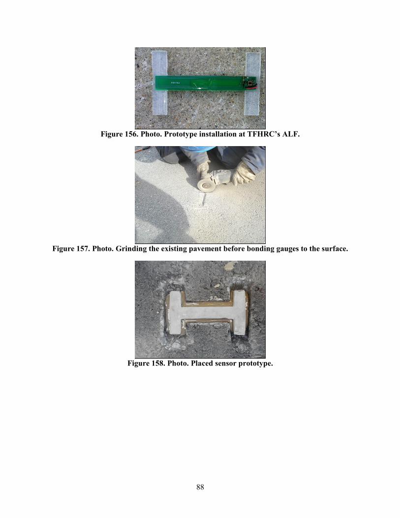
88
Figure 156. Photo. Prototype installation at TFHRC’s ALF.
Figure 157. Photo. Grinding the existing pavement before bonding gauges to the surface.
Figure 158. Photo. Placed sensor prototype.
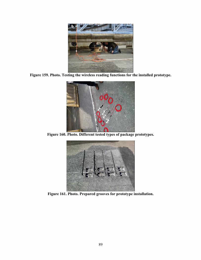
89
Figure 159. Photo. Testing the wireless reading functions for the installed prototype.
Figure 160. Photo. Different tested types of package prototypes.
Figure 161. Photo. Prepared grooves for prototype installation.

90
Figure 162. Photo. Special epoxy used to bond gauges to surface.
Figure 163. Photo. Installed prototypes.
An integrated prototype of the sensor was also installed at the ALF facility at TFHRC. The objective was to evaluate the short-term survivability and basic wireless functionalities of the sensor after applying the loading cycles. The results from this experiment were used to help refine the sensor electronics and the wireless communications protocols. Details of these refinements are discussed in chapters 2 and 3 of this report.
In addition, different prototypes of the packaging system were installed during a construction project in Michigan. Regular strain gauges were included in the packages. During installation, a procedure was used that did not cause any delays to construction. The gauges were laid just ahead of the compactor and secured with small HMA patches (see figure 164 through figure 167). The survivability rate dropped to 25 percent mainly because of the high strains on the wires during compaction. A total of 75 percent of the gauges that survived were placed in the transverse direction.

91
Figure 164. Photo. Installation of the prototype packaging system installed during a
construction project near Lansing, MI.
Figure 165. Photo. Specimen preparation and placement.
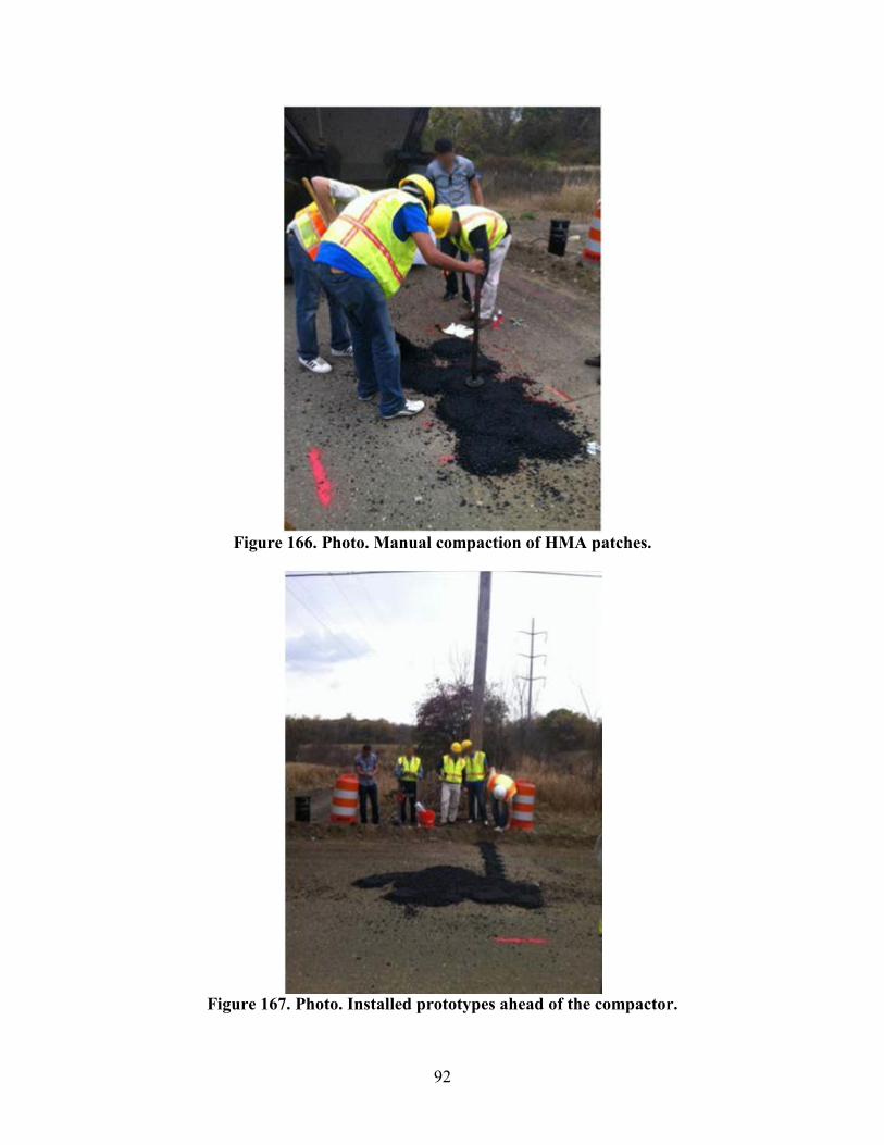
92
Figure 166. Photo. Manual compaction of HMA patches.
Figure 167. Photo. Installed prototypes ahead of the compactor.

93
5.4 CONCLUSION
In this chapter, a packaging system was designed and manufactured to encase the sensing modules. The package was designed so that it has a similar shape to existing systems and can be installed using existing installation procedures. Nonmetallic materials were used so that it allows for RF communication. A layered system mainly consisting of Araldite® GY-6010 epoxy, polyurethane foam, and mineral-filled urethane casting resin was used to provide the required mechanical and thermal protections for field installation. The system, entirely built in-house, was tested under a laboratory setup simulating field conditions as well as in construction projects.


95
CHAPTER 6. LABORATORY FATIGUE TESTING AND DEVELOPMENT OF SENSOR-SPECIFIC DAMAGE PROGNOSIS ALGORITHMS
This chapter focuses on evaluating the performance of the sensor for fatigue testing. The main objective is to develop a robust data interpretation algorithm that is able to use the diminished data provided by the sensor to achieve reasonable predictive capabilities comparable to what is obtained using conventional measuring techniques (conventional strain gauges). The time compressed cumulative data provided by the sensor result in a loss of information. A set of laboratory tests were designed to quantify and characterize the effect of these losses. The objective is to recreate the damage index variation curves using only the cumulative information tracked by the sensor.
6.1 DATA INTERPRETATION ALGORITHMS
Measured peak strain distributions in a pavement are approximated by Gaussian distributions for all of the considered cases. The variation of the strain amplitude over time is due to the increase of the compliance (i.e., induction of fatigue damage in the specimen). Figure 168 shows the strain amplitude variation of a concrete beam over time under cyclic loading at a constant amplitude. The strain amplitude is shown to increase, which explains the loss in the elastic modulus of the beam. This increase in amplitude causes the increase of the output voltage amplitude that is recorded by the sensor.
The considered hypothesis is that a shift in the measured strain distributions toward higher strains over time is indicative of damage accumulation. Thus, monitoring the mean and the standard deviation of the distribution over time and tracking the mean variations allow researchers to determine the levels of strains that are induced in the specimen between reading periods. By determining these response levels, the compliance can be evaluated. A simplified model, described in this section, shows how these measurements are obtained and related to damage.
0
0.0002
0.0004
0.0006
0.0008
0.001
0.0012
0 20000 40000 60000 80000 100000 120000 140000 160000
Stra
in A
mpl
itude
(με)
Number of Cycles
Strain Amplitude Variation
Figure 168. Graph. Strain amplitude variation of a concrete beam under cyclic load with
constant amplitude.
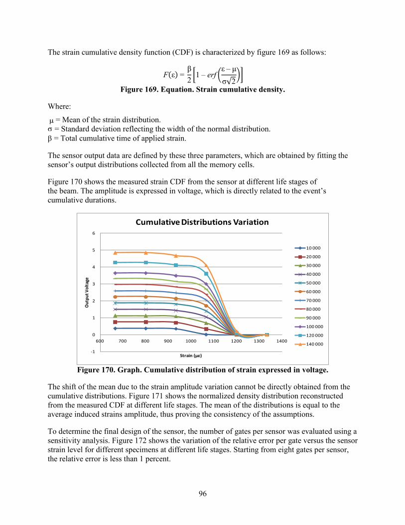
96
The strain cumulative density function (CDF) is characterized by figure 169 as follows:
F(ε) = β2�1 ‒ erf �
ε ‒ μσ√2
��
Figure 169. Equation. Strain cumulative density.
Where:
µ = Mean of the strain distribution. σ = Standard deviation reflecting the width of the normal distribution. β = Total cumulative time of applied strain.
The sensor output data are defined by these three parameters, which are obtained by fitting the sensor’s output distributions collected from all the memory cells.
Figure 170 shows the measured strain CDF from the sensor at different life stages of the beam. The amplitude is expressed in voltage, which is directly related to the event’s cumulative durations.
-1
0
1
2
3
4
5
6
600 700 800 900 1000 1100 1200 1300 1400
Out
put V
olta
ge
Strain (με)
Cumulative Distributions Variation
10 000
20 000
30 000
40 000
50 000
60 000
70 000
80 000
90 000
100 000
120 000
140 000
Figure 170. Graph. Cumulative distribution of strain expressed in voltage.
The shift of the mean due to the strain amplitude variation cannot be directly obtained from the cumulative distributions. Figure 171 shows the normalized density distribution reconstructed from the measured CDF at different life stages. The mean of the distributions is equal to the average induced strains amplitude, thus proving the consistency of the assumptions.
To determine the final design of the sensor, the number of gates per sensor was evaluated using a sensitivity analysis. Figure 172 shows the variation of the relative error per gate versus the sensor strain level for different specimens at different life stages. Starting from eight gates per sensor, the relative error is less than 1 percent.
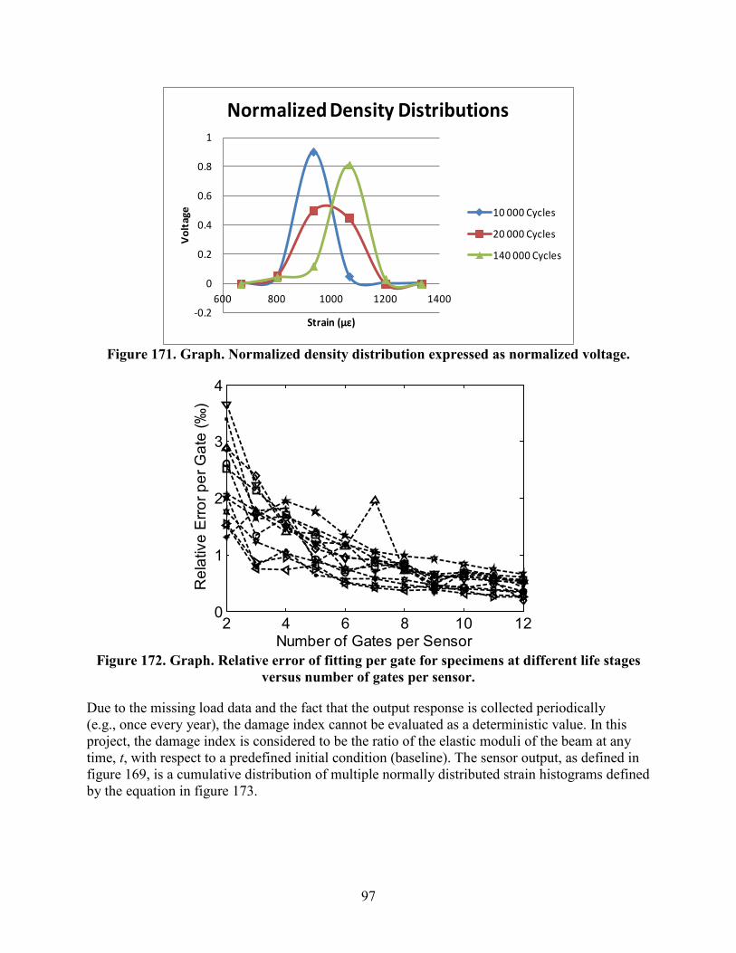
97
-0.2
0
0.2
0.4
0.6
0.8
1
600 800 1000 1200 1400
Vol
tage
Strain (με)
Normalized Density Distributions
10 000 Cycles
20 000 Cycles
140 000 Cycles
Figure 171. Graph. Normalized density distribution expressed as normalized voltage.
2 4 6 8 10 120
1
2
3
4
Number of Gates per Sensor
Rel
ativ
e E
rror p
er G
ate
(‰)
Figure 172. Graph. Relative error of fitting per gate for specimens at different life stages
versus number of gates per sensor.
Due to the missing load data and the fact that the output response is collected periodically (e.g., once every year), the damage index cannot be evaluated as a deterministic value. In this project, the damage index is considered to be the ratio of the elastic moduli of the beam at any time, t, with respect to a predefined initial condition (baseline). The sensor output, as defined in figure 169, is a cumulative distribution of multiple normally distributed strain histograms defined by the equation in figure 173.

98
( )( ) ( )
2 2
2 22 22 22 2
i
ii
i i
h e eε µ ε µσ σ
εα αεπσ πσ
− −− −= =∑
Figure 173. Equation. Cumulative distribution.
The standard deviation, the cumulative loading time, and the mean of the cumulative strain are evaluated from the parameters of the strain loading distributions shown in figure 174 through figure 176.
ii
α α=∑
Figure 174. Equation. Cumulative loading time.
[ ] ii
iE αε µ
α=∑
Figure 175. Equation. Mean of the cumulative strain.
[ ] 2ii
iVar αε σ
α=∑
Figure 176. Equation. Standard deviation.
Using figure 175 and figure 176, the mean and the standard deviation of the applied strain amplitude at a time t can be evaluated using two consecutive readings, as expressed by the following equations in figure 177 and figure 178.
( )t
µαµ
α∆
=∆
Figure 177. Equation. Mean of the applied strain amplitude at time t.
( ) 1/22
t
σ ασ
α
∆ = ∆
Figure 178. Equation. Standard deviation of the applied strain amplitude at time t.
Once the mean and the standard deviation of the strain distributions are evaluated, Taylor series with exact derivation are used to derive the mean and the variance of the damage coefficient, which are given by figure 179 and figure 180.
[ ] 0
N
E D µµ
=
Figure 179. Equation. Mean of the damage coefficient.

99
[ ]2 2 20 02 4
N
N N
Var D σ µ σµ µ
= +
Figure 180. Equation. Variance of the damage coefficient.
The reliability index, considered with respect to a damage coefficient equal to 0, is then evaluated as follows:
02 2
2 00 2
N
N
µβµ σσµ
=
+
Figure 181. Equation. Reliability index.
The probability of failure, which is defined as the probability of the damage coefficient being less than 0, is then given by the following equation:
( )2
1 12 2
P failure erf µ
σ
−= +
Figure 182. Equation. Probability of failure.
Expressing the failure of the structure in terms of probability of failure is more meaningful, given that the damage coefficient at failure is not a predefined value, and it varies from one specimen to another.
6.2 ALGORITHM EVALUATION USING CONCRETE BEAM FLEXURAL BENDING FATIGUE TESTS
A total of 23 plain PCC three-point single-edge notched beam specimens were tested under constant and variable amplitude fatigue loading. Two beam sizes were considered: the large-sized beams had a span of 16 inches (406.4 mm), a depth of 4 inches (101.6 mm), and a width of 4 inches (101.6 mm). The small-sized beams had a span of 8 inches (203.2 mm), a depth of 2 inches (50.8 mm), and a width of 2 inches (50.8 mm). The notch to depth ratio for each specimen was 0.35. A COD gauge was used to measure the crack mouth opening and was attached to a pair of knife edges, which were mounted to the bottom face of the beam by a fast-drying epoxy resin, as recommended by Shah et al.(6) Each specimen was subjected to a 2-Hz cyclical load. Ten specimens were subjected to constant amplitude loading using a stress ratio (max load/peak load) of 0.85 and 0.95. The other specimens were subjected to variable loading in which both the R ratio (minimum/maximum load) and the stress ratio were varied at several stages throughout the test.
The concrete mix used in this research consisted of ASTM C-150 type I cement, a natural sand, and a limestone coarse aggregate (nominal maximum size of 1 inch (25.4 mm)). The water-to-cement ratio was 0.45, and the air content was 6.5 percent. The unit weight was 142 lb/ft3 (22.7 kg/m3).
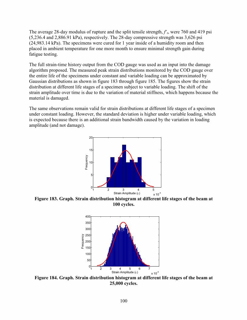
100
The average 28-day modulus of rupture and the split tensile strength, f’t, were 760 and 419 psi (5,236.4 and 2,886.91 kPa), respectively. The 28-day compressive strength was 3,626 psi (24,983.14 kPa). The specimens were cured for 1 year inside of a humidity room and then placed in ambient temperature for one more month to ensure minimal strength gain during fatigue testing.
The full strain-time history output from the COD gauge was used as an input into the damage algorithm proposed. The measured peak strain distributions monitored by the COD gauge over the entire life of the specimens under constant and variable loading can be approximated by Gaussian distributions as shown in figure 183 through figure 185. The figures show the strain distribution at different life stages of a specimen subject to variable loading. The shift of the strain amplitude over time is due to the variation of material stiffness, which happens because the material is damaged.
The same observations remain valid for strain distributions at different life stages of a specimen under constant loading. However, the standard deviation is higher under variable loading, which is expected because there is an additional strain bandwidth caused by the variation in loading amplitude (and not damage).
1 2 3 4 5x 10⁻⁴
0
5
10
15
20
Strain Amplitude (ε)
Freq
uenc
y
Figure 183. Graph. Strain distribution histogram at different life stages of the beam at
100 cycles.
1 2 3 4 5 6 7x 10⁻⁴
0
50
100
150
200
250
300
350
400
Strain Amplitude (ε)
Freq
uenc
y
Figure 184. Graph. Strain distribution histogram at different life stages of the beam at
25,000 cycles.
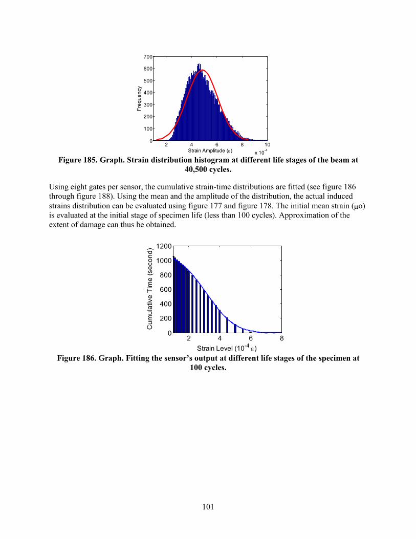
101
2 4 6 8 10x 10-4
0
100
200
300
400
500
600
700
Strain Amplitude (ε)
Freq
uenc
y
Figure 185. Graph. Strain distribution histogram at different life stages of the beam at
40,500 cycles.
Using eight gates per sensor, the cumulative strain-time distributions are fitted (see figure 186 through figure 188). Using the mean and the amplitude of the distribution, the actual induced strains distribution can be evaluated using figure 177 and figure 178. The initial mean strain (µ o) is evaluated at the initial stage of specimen life (less than 100 cycles). Approximation of the extent of damage can thus be obtained.
2 4 6 80
200
400
600
800
1000
1200
Strain Level (10-4 ε)
Cum
ulat
ive
Tim
e (s
econ
d)
Figure 186. Graph. Fitting the sensor’s output at different life stages of the specimen at
100 cycles.
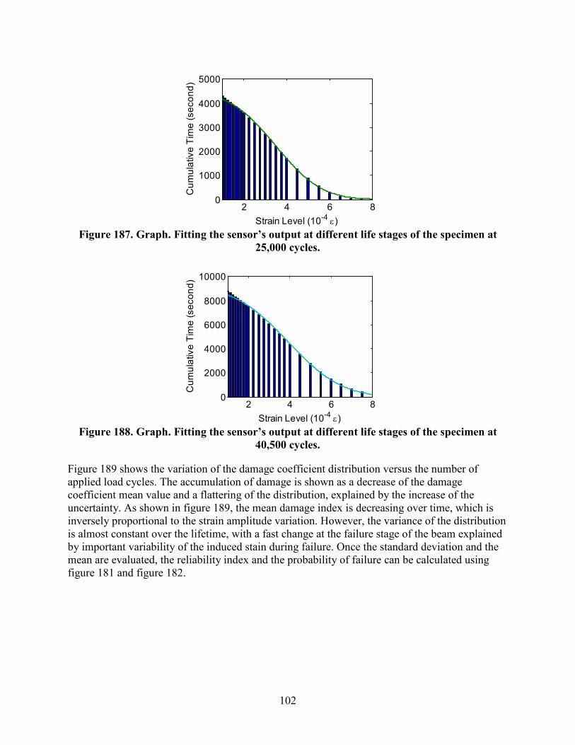
102
2 4 6 80
1000
2000
3000
4000
5000
Strain Level (10-4 ε)
Cum
ulat
ive
Tim
e (s
econ
d)
Figure 187. Graph. Fitting the sensor’s output at different life stages of the specimen at
25,000 cycles.
2 4 6 80
2000
4000
6000
8000
10000
Strain Level (10-4 ε)
Cum
ulat
ive
Tim
e (s
econ
d)
Figure 188. Graph. Fitting the sensor’s output at different life stages of the specimen at
40,500 cycles.
Figure 189 shows the variation of the damage coefficient distribution versus the number of applied load cycles. The accumulation of damage is shown as a decrease of the damage coefficient mean value and a flattering of the distribution, explained by the increase of the uncertainty. As shown in figure 189, the mean damage index is decreasing over time, which is inversely proportional to the strain amplitude variation. However, the variance of the distribution is almost constant over the lifetime, with a fast change at the failure stage of the beam explained by important variability of the induced stain during failure. Once the standard deviation and the mean are evaluated, the reliability index and the probability of failure can be calculated using figure 181 and figure 182.
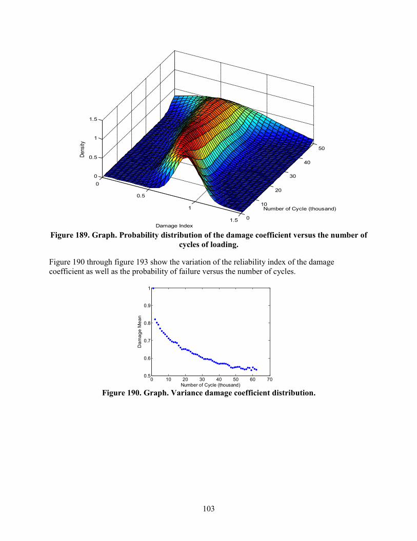
103
0
0.5
1
1.5 0
10
20
30
40
50
0
0.5
1
1.5
Number of Cycle (thousand)
Damage Index
Dens
ity
Figure 189. Graph. Probability distribution of the damage coefficient versus the number of
cycles of loading.
Figure 190 through figure 193 show the variation of the reliability index of the damage coefficient as well as the probability of failure versus the number of cycles.
0 10 20 30 40 50 60 700.5
0.6
0.7
0.8
0.9
1
Number of Cycle (thousand)
Dam
age
Mea
n
Figure 190. Graph. Variance damage coefficient distribution.
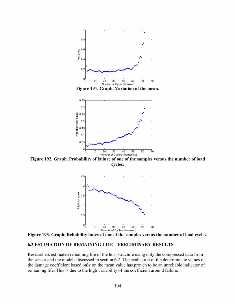
104
0 10 20 30 40 50 60 700
0.2
0.4
0.6
0.8
1
Number of Cycle (thousand)
Var
ianc
e
Figure 191. Graph. Variation of the mean.
0 10 20 30 40 50 60 700
0.05
0.1
0.15
0.2
0.25
0.3
0.35
Number of Cycles (thousands)
Pro
babi
lity
of F
ailu
re
Figure 192. Graph. Probability of failure of one of the samples versus the number of load
cycles.
0 10 20 30 40 50 60 700
0.5
1
1.5
2
2.5
Number of Cycles (thousand)
Rlia
bilit
y In
dex
Figure 193. Graph. Reliability index of one of the samples versus the number of load cycles.
6.3 ESTIMATION OF REMAINING LIFE—PRELIMINARY RESULTS
Researchers estimated remaining life of the host structure using only the compressed data from the sensor and the models discussed in section 6.2. The evaluation of the deterministic values of the damage coefficient based only on the mean value has proven to be an unreliable indicator of remaining life. This is due to the high variability of the coefficient around failure.

105
Table 5 shows the reliability index, the damage coefficient, and the probability of failure just before failure. Due to the high variability of the damage index at failure, the probability of failure just before failure and the reliability index are not consistent. For a better remaining life estimation, the damage index variability at failure needs to be accounted for.
Table 5. Reliability index, probability of failure, and damage coefficient at failure for different specimens.
Sample
Reliability Index at Failure
Probability of Failure Just
Before Failure
Damage Coefficient at Failure
1 0.54 0.29 0.3 2 0.77 0.25 0.44 3 0.72 0.31 0.56 4 0.51 0.31 0.46
6.3.1 Mechanistic-Empirical Approach
Figure 194 and figure 195 show the linear damage accumulation rule that is used in mechanistic-empirical (M-E) models. The coefficients,βi , are calibrated for every specimen using the sensor damage reading at the damage inflection point. Subramaniam et al. observed that under constant amplitude loading, the inflection point between the deceleration and the acceleration cracking region occurs at approximately 40 to 50 percent of the total life of the specimen.(7) Thus, the coefficients pertaining to the first half of the specimen’s life should be similar to the second half. Once the coefficients are known, a remaining life prediction can be made.
D =�1Nf
Figure 194. Equation. Linear damage accumulation rule.
Log(Nf) = β0 �1
SR�
β1
+ β2
Figure 195. Equation. Remaining life.
Table 6 shows the predicted remaining life using the described method based on the sensor output (models described in section 6.2) and based on the calibrated coefficient of the linear damage accumulation rule for different tested specimens. The loading of the specimens was stopped, and the remaining life was estimated using the different methods and based on the evaluated damage at that stage. The tests were then continued until failure in order to record the actual remaining life. As observed in the results, for the considered cases, the predictions evaluated using the localized sensor data are closer to reality than linear damage accumulation predictions based on averaged values.
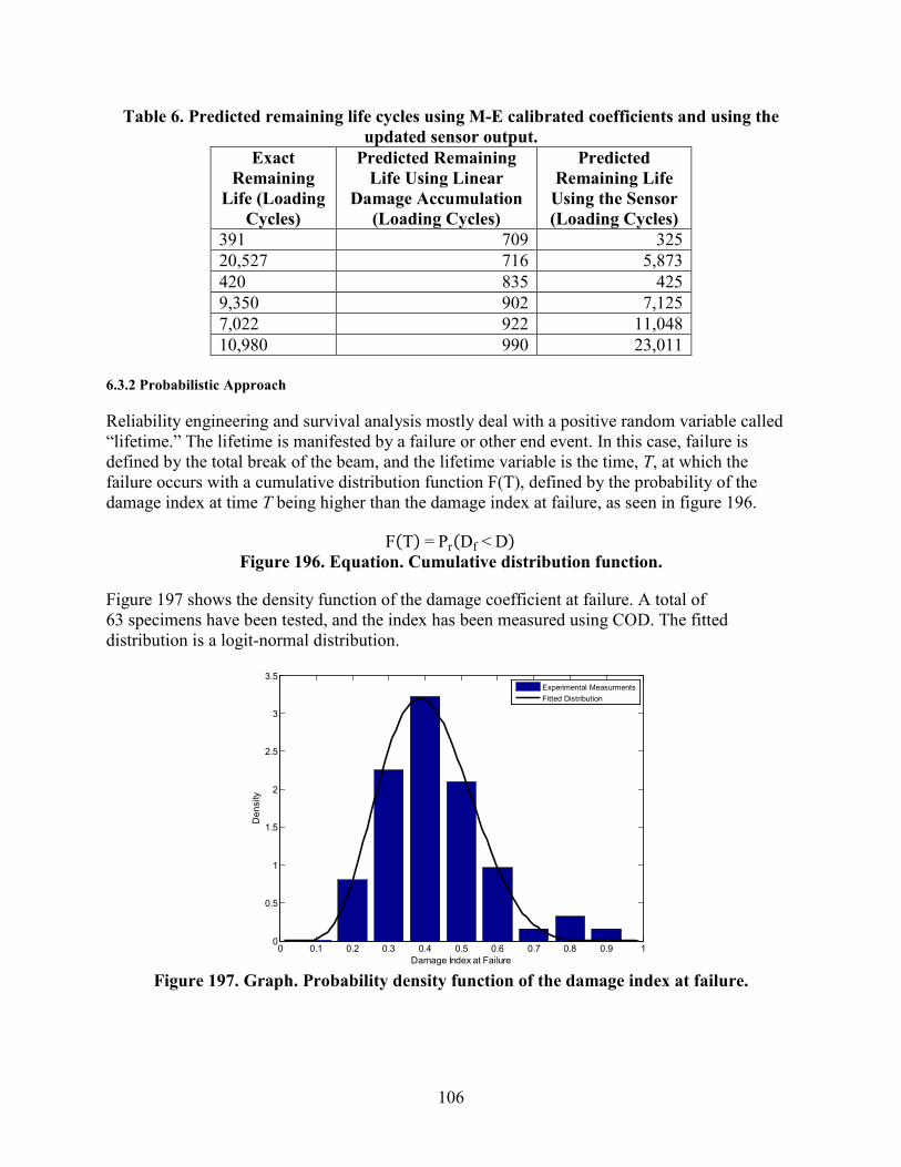
106
Table 6. Predicted remaining life cycles using M-E calibrated coefficients and using the updated sensor output.
Exact Remaining
Life (Loading Cycles)
Predicted Remaining Life Using Linear
Damage Accumulation (Loading Cycles)
Predicted Remaining Life
Using the Sensor (Loading Cycles)
391 709 325 20,527 716 5,873 420 835 425 9,350 902 7,125 7,022 922 11,048 10,980 990 23,011
6.3.2 Probabilistic Approach
Reliability engineering and survival analysis mostly deal with a positive random variable called “lifetime.” The lifetime is manifested by a failure or other end event. In this case, failure is defined by the total break of the beam, and the lifetime variable is the time, T, at which the failure occurs with a cumulative distribution function F(T), defined by the probability of the damage index at time T being higher than the damage index at failure, as seen in figure 196.
F(T) = Pr(Df < D) Figure 196. Equation. Cumulative distribution function.
Figure 197 shows the density function of the damage coefficient at failure. A total of 63 specimens have been tested, and the index has been measured using COD. The fitted distribution is a logit-normal distribution.
0 0.1 0.2 0.3 0.4 0.5 0.6 0.7 0.8 0.9 10
0.5
1
1.5
2
2.5
3
3.5
Damage Index at Failure
Den
sity
Experimental MeasurmentsFitted Distribution
Figure 197. Graph. Probability density function of the damage index at failure.

107
Researchers evaluated the survival probability function of the specimens based on the evaluated damage index obtained using the sensor and also evaluated the probability density function of the index at failure.
The remaining life CDF is defined using the law of conditional probability, the condition being that the beam did not fail at time t = x.
Fx(T) = Pr(x < T < x + t)
Pr(x < T) =F(x + t) ‒ F(x)
F�(x)
Figure 198. Equation. Remaining life CDF.
The corresponding survival probability function of the beam is given by the following equation:
Fx���(T) = F�(x + t)
F�(x)
Figure 199. Equation. Survival probability function of the beam.
Remaining life is then estimated to be the expectation of the survival probability function:
Rem = E(Tt)=∫ F�(u) du∞
tF�(t)
Figure 200. Equation. Expectation of the survival probability function.
However, the life probability function is not defined.
Remaining life should be expressed as a function of the damage index probability function (the only information that the sensor can provide). Using a change of variable, figure 199 can be expressed as a function of the damage index.
Rem = E(Tt)=
∫ F�d(D) dDdDdt
∞t
F�d(D)
Figure 201. Equation. Function of the damage index.
Where dD/dt is the variation of the damage index with respect to time evaluated by fitting a shape function to the discrete values evaluated using the sensor. The assumed shape functions are linear, exponential, and arcsine.
Figure 202 shows the normalized predicted remaining life (see figure 201) derived using the developed methodology based solely on the sensor’s output. The associated probability (from figure 198) is shown in figure 203. As the number of applied cycles increases, more readings are incorporated into the adaptive models, which are used as fitting points. This implies that as the specimen gets closer to failure, the prediction accuracy improves, which is shown by the higher probability (reliability) of the estimated remaining life.
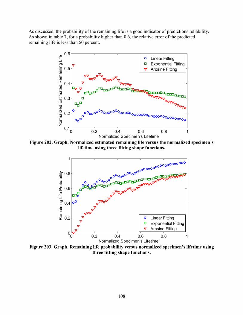
108
As discussed, the probability of the remaining life is a good indicator of predictions reliability. As shown in table 7, for a probability higher than 0.6, the relative error of the predicted remaining life is less than 50 percent.
0 0.2 0.4 0.6 0.8 10.1
0.2
0.3
0.4
0.5
0.6
Normalized Specimen's Lifetime
Nor
mal
ized
Est
imat
ed R
emai
ning
Life
Linear FittingExponential FittingArcsine Fitting
Figure 202. Graph. Normalized estimated remaining life versus the normalized specimen’s
lifetime using three fitting shape functions.
0 0.2 0.4 0.6 0.8 10
0.2
0.4
0.6
0.8
1
Normalized Specimen's Lifetime
Rem
aini
ng L
ife P
roba
bilit
y
Linear FittingExponential FittingArcsine Fitting
Figure 203. Graph. Remaining life probability versus normalized specimen’s lifetime using
three fitting shape functions.

109
Table 7. Estimated remaining life using the different fitting shape function.
Exact Remaining
Life
Exponential Shape Function Linear Shape Function Arcsine Shape Function Remaining
Life Prob. Error
(Percent) Remaining
Life Prob. Error
(Percent) Remaining
Life Prob. Error
(Percent) 0.9 0.1809 0.6406 71.91 0.3003 0.6071 59.97 0.4064 0.2133 49.36 0.8 0.2014 0.6565 59.86 0.3435 0.6149 45.65 0.4347 0.3459 36.53 0.7 0.2026 0.6913 49.74 0.3539 0.6309 34.61 0.4207 0.4346 27.93 0.6 0.2116 0.7688 38.84 0.3703 0.6746 22.97 0.4221 0.5455 17.79 0.5 0.2031 0.807 29.69 0.3629 0.6959 13.71 0.3881 0.5988 11.19 0.4 0.1919 0.8444 20.81 0.3496 0.717 5.04 0.3481 0.6436 5.19 0.3 0.1796 0.8751 12.04 0.3368 0.735 3.68 0.3115 0.6784 1.15 0.2 0.1719 0.9068 2.81 0.3287 0.7575 12.87 0.2836 0.7218 8.36 0.1 0.1617 0.9315 6.17 0.3171 0.7748 21.71 0.2525 0.757 15.25
6.4 DATA IMPUTATION—MISSING FULL-FIELD DATA GENERATION
Several researchers studied the effects of traffic wander on pavement performance.(8–10) It was shown that the wheel wander is critical because it determines the distribution of load location on the pavement as well as the frequency at which a point is loaded. Measurements from a field study conducted by Timm and Priest showed that wheel wander tends to be normally distributed with a standard deviation ranging from 8 to 24 inches (203.2 to 609.6 mm).(11) Given that only a limited number of sensors can be implemented on a pavement section, it is critical to generate full field data and incorporate the effect of traffic wander in the fatigue prediction algorithms that use the data collected from the implemented sensors. In addition, the obtained full field data can be used to backcalculate the traffic wander distribution at a given location by tracking strain peaks in the generated data in a pavement cross section. These problems could be considered as missing data problems. Several techniques have been used to generate missing data from a set of measurements at a set of predetermined locations. In this report, the Kriging technique was implemented to test its applicability to the specific data collected from the developed sensors.
The novel self-powered microsensors presented in chapter 2 of this report are capable of continuously monitoring local strains of the host structure. They implement the level-crossing counting algorithm. A network of N implemented sensors will generate N random variables ( )NXX ,...,1 that describe the response of the system at a given state.
Examples of strain output distributions are shown in figure 204. The shown data are obtained from the model of piezo-powered sensors attached on a simply supported beam with dimensions 12 × 1 × 1 inch (304.8 × 25.4 × 25.4 mm) and subject to a random applied loading at its center, inducing a mid-span deformation of amplitude varying between 0.04 and 0.12 inches (1.02 and 3.04 mm). PZT piezoelectric generators with dimensions of 0.4 × 0.2 × 0.004 inches (10.16 × 5.08 × 0.10 mm) were used in the simulation. The generators’ output were obtained at three different positions (x = 2.9, 3.7, and 4.9 inches (73.66, 93.98, and 124.46 mm)), where x is the position of the piezo-strip center measured from the left end of the beam. The cumulative strain data at each sensor node can be fit to a variation of the exponential discrete probability distribution of the form f(y) = θ1e-θ2y2 + θ3y , where y = (1,2,...,7) is the memory cell number also associated with a strain amplitude level, and θT = (θ1,θ2,θ3) represents the parameter of the strain
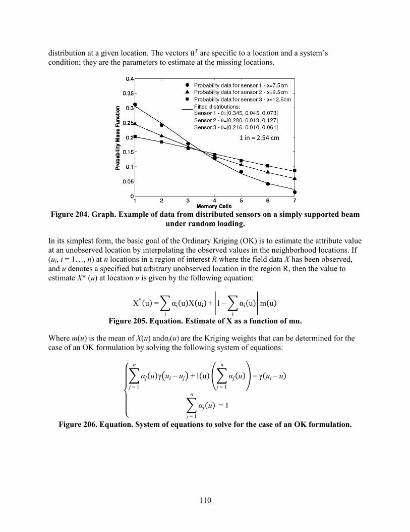
110
distribution at a given location. The vectors θT are specific to a location and a system’s condition; they are the parameters to estimate at the missing locations.
1 in = 2.54 cm
Figure 204. Graph. Example of data from distributed sensors on a simply supported beam
under random loading.
In its simplest form, the basic goal of the Ordinary Kriging (OK) is to estimate the attribute value at an unobserved location by interpolating the observed values in the neighborhood locations. If (ui, i = 1…, n) at n locations in a region of interest R where the field data X has been observed, and u denotes a specified but arbitrary unobserved location in the region R, then the value to estimate X* (u) at location u is given by the following equation:
X*(u) =� αi(u)X(ui)i
+ �1 ‒� αi(u)i
�m(u)
Figure 205. Equation. Estimate of X as a function of mu.
Where m(u) is the mean of X(u) andαi(u) are the Kriging weights that can be determined for the case of an OK formulation by solving the following system of equations:
⎩⎪⎪⎨
⎪⎪⎧� αj(u)γ�ui ‒ uj� + l(u)�� αj(u)
n
j = 1
�= γ(ui ‒ u)n
j = 1
� αj(u)n
j = 1
= 1
�
Figure 206. Equation. System of equations to solve for the case of an OK formulation.

111
Where:
(ui – uj) = Distance between location i and location j. (ui – u) = Distance between location i and the location to be estimated. l(u) = Lagrange parameter. γ = Predefined semi-variance property that expresses the degree of spatial dependence between points.
A simply supported beam setup was initially used to test and tune the developed techniques under simplified strain distributions; the load configuration consisted of a moving concentrated load for generating linear strains along the beam and a distributed load for quadratic strains. Simulated strain data were generated using the piezoelectric generator and the sensor models described in chapters 2 and 3. The frequency distribution of strain levels at a selected reference location (x = 3.7 inches (93.98 mm)) of the beam was estimated for different loading and known data combinations. One million cycles of random amplitude for each loading combination were simulated. Values of γ in figure 206 were extracted using linear and quadratic variograms. It was determined that higher order variograms do not improve the obtained estimations for the considered strains. It was also observed that a better estimation is obtained when the missing data point is located between the known points. For example, the cumulative relative error when the known couple is located at 3.34 and 4.1 inches (84.84 and 104.14 mm) is 0.0193, while it is equal to 0.0567 for the case of a known couple at 4.1 and 5.3 inches (104.14 and 134.62 mm). The error decreases to 0.0433 for 3.34 and 5.3 inches (84.84 and 134.62 mm) even though the relative distances to the point at which an estimate is desired are the same.
An example of estimated probabilities obtained using the Kriging technique is shown in figure 207. The probability mass function of the strain levels at the location x = 3.7 inches (93.98 mm) if a sensor was to be installed at that position is also shown. Second order polynomial variograms were used for this case. The computed errors are 0.0415, 0.0694, and 0.072, respectively, for the cases 3.34, 4.1, and 4.5 inches (84.84, 104.14, and 114.3 mm), 3.34, 5.3, and 5.7 inches (84.84, 134.62, and 144.78 mm), and 4.1, 5.3, and 5.7 inches (104.14, 134.62, and 144.78 mm).
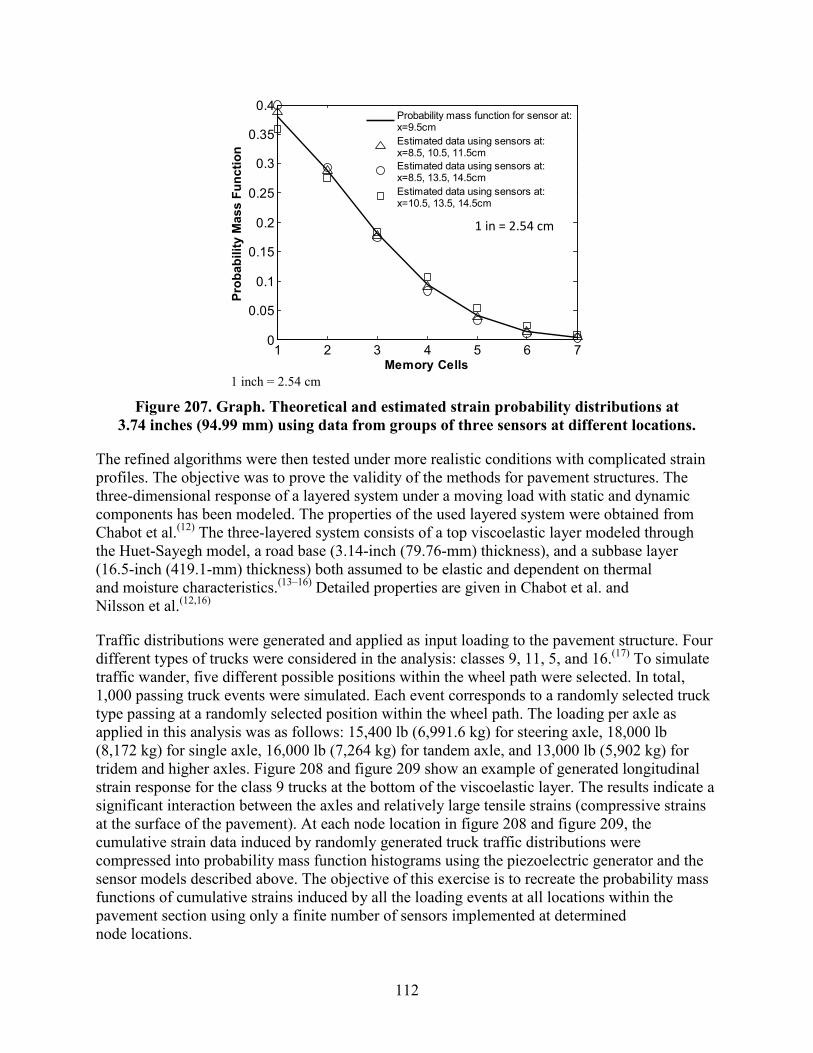
112
1 2 3 4 5 6 70
0.05
0.1
0.15
0.2
0.25
0.3
0.35
0.4
Memory Cells
Prob
abili
ty M
ass
Func
tion
Probability mass function for sensor at:x=9.5cmEstimated data using sensors at:x=8.5, 10.5, 11.5cmEstimated data using sensors at:x=8.5, 13.5, 14.5cmEstimated data using sensors at:x=10.5, 13.5, 14.5cm
1 in = 2.54 cm
1 inch = 2.54 cm
Figure 207. Graph. Theoretical and estimated strain probability distributions at 3.74 inches (94.99 mm) using data from groups of three sensors at different locations.
The refined algorithms were then tested under more realistic conditions with complicated strain profiles. The objective was to prove the validity of the methods for pavement structures. The three-dimensional response of a layered system under a moving load with static and dynamic components has been modeled. The properties of the used layered system were obtained from Chabot et al.(12) The three-layered system consists of a top viscoelastic layer modeled through the Huet-Sayegh model, a road base (3.14-inch (79.76-mm) thickness), and a subbase layer (16.5-inch (419.1-mm) thickness) both assumed to be elastic and dependent on thermal and moisture characteristics.(13–16) Detailed properties are given in Chabot et al. and Nilsson et al.(12,16)
Traffic distributions were generated and applied as input loading to the pavement structure. Four different types of trucks were considered in the analysis: classes 9, 11, 5, and 16.(17) To simulate traffic wander, five different possible positions within the wheel path were selected. In total, 1,000 passing truck events were simulated. Each event corresponds to a randomly selected truck type passing at a randomly selected position within the wheel path. The loading per axle as applied in this analysis was as follows: 15,400 lb (6,991.6 kg) for steering axle, 18,000 lb (8,172 kg) for single axle, 16,000 lb (7,264 kg) for tandem axle, and 13,000 lb (5,902 kg) for tridem and higher axles. Figure 208 and figure 209 show an example of generated longitudinal strain response for the class 9 trucks at the bottom of the viscoelastic layer. The results indicate a significant interaction between the axles and relatively large tensile strains (compressive strains at the surface of the pavement). At each node location in figure 208 and figure 209, the cumulative strain data induced by randomly generated truck traffic distributions were compressed into probability mass function histograms using the piezoelectric generator and the sensor models described above. The objective of this exercise is to recreate the probability mass functions of cumulative strains induced by all the loading events at all locations within the pavement section using only a finite number of sensors implemented at determined node locations.
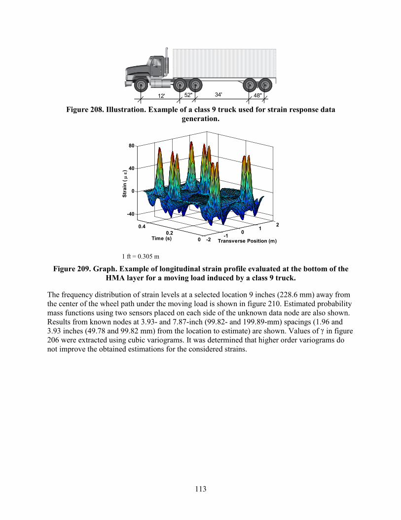
113
52'' 48'' 12' 34'
Figure 208. Illustration. Example of a class 9 truck used for strain response data generation.
-2-1
01
2
00.2
0.4
-40
0
40
80
Transverse Position (m)Time (s)
Stra
in ( µ ε)
1 ft = 0.305 m
Figure 209. Graph. Example of longitudinal strain profile evaluated at the bottom of the HMA layer for a moving load induced by a class 9 truck.
The frequency distribution of strain levels at a selected location 9 inches (228.6 mm) away from the center of the wheel path under the moving load is shown in figure 210. Estimated probability mass functions using two sensors placed on each side of the unknown data node are also shown. Results from known nodes at 3.93- and 7.87-inch (99.82- and 199.89-mm) spacings (1.96 and 3.93 inches (49.78 and 99.82 mm) from the location to estimate) are shown. Values of γ in figure 206 were extracted using cubic variograms. It was determined that higher order variograms do not improve the obtained estimations for the considered strains.
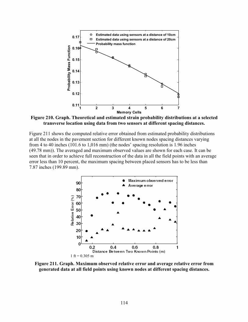
114
1 2 3 4 5 6 70.11
0.12
0.13
0.14
0.15
0.16
0.17
Memory Cells
Prob
abili
ty M
ass
Func
tion
Estimated data using sensors at a distance of 10cmEstimated data using sensors at a distance of 20cmProbability mass function
Figure 210. Graph. Theoretical and estimated strain probability distributions at a selected
transverse location using data from two sensors at different spacing distances.
Figure 211 shows the computed relative error obtained from estimated probability distributions at all the nodes in the pavement section for different known nodes spacing distances varying from 4 to 40 inches (101.6 to 1,016 mm) (the nodes’ spacing resolution is 1.96 inches (49.78 mm)). The averaged and maximum observed values are shown for each case. It can be seen that in order to achieve full reconstruction of the data in all the field points with an average error less than 10 percent, the maximum spacing between placed sensors has to be less than 7.87 inches (199.89 mm).
1 ft = 0.305 m
Figure 211. Graph. Maximum observed relative error and average relative error from generated data at all field points using known nodes at different spacing distances.

115
6.5 CONCLUSION
In this chapter, a sensor-specific data interpretation algorithm for predicting remaining fatigue life of a pavement structure was developed using cumulative limited compressed strain data stored in the sensor memory chip. The algorithm was verified using actual laboratory fatigue test results of a notched concrete beam under constant, variable, and random loading histories.


117
CHAPTER 7. CONCLUSION
The research in this project led to the development of a novel sensor system for continuous health monitoring of pavement structures. The system consists of a self-powered wireless sensor capable of detecting fatigue damage in pavement structures under actual traffic and environmental load history. The developed system is based on the integration of a piezoelectric transducer with an array of ultra-low power FG computational circuits. A miniaturized sensor was developed and tested. It was shown that it is capable of continuous battery-less monitoring of strain events integrated over the occurrence duration time.
Successful development of the proposed strain sensor could dramatically transform the economics of pavement preservation/management and ultimately improve the serviceability of pavements. The developed system consists of a network of low-cost sensors distributed along the pavement. Each sensor node is self-powered and capable of continuously monitoring and storing the dynamic strain levels in the host pavement structure. The strain data are stored on-board the sensor, which consists of the self-powered sensor strip and small-scale electronics. The data from all the sensors are periodically uploaded wirelessly to a central database. The sensor can be read through standard RF transmission using a RF reader that is either manually operated or mounted on a moving vehicle. By directly outfitting service vehicles with low-cost RF transponders, the roads can be frequently monitored to detect changes in structural integrity that may not only foreshadow a future crack/distress manifestation but also allow for more accurate scheduling of preservation actions. It should be noted that only a single RF reader is needed to inspect the sensor network.
The main characteristics of the new sensor are as follows:
• Self-powered, continuous, and autonomous sensing. Testing of the sensor showed that it is able to operate using only self-generated electrical energy harvested directly from the sensing signal induced by a piezoelectric transducer attached to the pavement.
• Autonomous computation and non-volatile storage of sensing variables. The design uses the physics of FG transistor injection principles for computing cumulative mechanical strain patterns experienced by the pavement structure. The design details and corresponding steps are detailed in chapter 2 of this report.
• Small size. The actual size of the analog electronics circuit, manufactured in a special small package, is 0.23 × 0.21 × 0.03 inches (5.84 × 5.33 × 0.76 mm). An interface board was designed and manufactured in-house. The board acts as an interface between the active piezoelectric element and the analog electronics. The board also contains all of the electronic circuitry that interfaces the sensor with the reading antenna. The board dimensions are 0.6 × 0.6 × 0.04 inches (15.24 × 15.24 × 1.01 mm). The size of the active piezoelectric element, used as sensor and source of energy, depends on the desired level of sensitivity and accuracy required at each measuring node. The amplitude of the measured strains determines the size of the transducer to be implemented. A minimum voltage of 2.3V is required at the piezo’s output to activate the gate’s memory system. Thus, for low-level strains, a bigger active area is required to generate the needed power.

118
During the current research, transducers varying from 0.78 × 0.04 × 0.007 inches (19.81 × 1.01 × 0.18 mm) to 2.36 × 0.4 × 0.07 inches (59.94 × 10.16 × 1.78 mm) were used. The complete system (analog electronics, interface board, and a piezoelectric element) are integrated in a package designed and manufactured in-house. The package was designed so that it has a similar shape to existing systems, and it can be installed using existing installation procedures that are accepted by SHAs and will not constitute a major disruption to current practices.
• Wireless communication. A novel RF communication module was designed in-house. The mixed mode module is specific for integration with the FG analog memories. It should be noted that commercially available RF modules cannot be associated with the used circuitry given the very low current levels in the system. The RF powering mode is dissociated from the computing and storage circuitry and is achieved by harvesting the RF signal. The salient modules of the RF module include: (1) ADC for digitizing the stored usage statistics, (2) charge-pumps for generating biases for erasing and remote initialization of the sensor, (3) encoding/decoding circuits for creating data packets with inherent clock/data recovery mechanisms, (4) state machine for command and control of the IC, and (5) RF interface circuitry operating at 13.56 MHz for harvesting energy from the reader signal and for wireless transmission of the sensor data. In addition, an external reader was designed and manufactured. The reader interfaces with an embedded antenna, which was also designed and manufactured in-house and fits the exact H-shape of the designed package. The embedded antenna is connected to the interface. Laboratory testing showed that the reading distance highly depends on the parasitic capacitances of the antennas (embedded antenna and external reader) as well as the parasitic capacitance at the sensors input. These capacitances are induced by the manufacturing process and cannot be predicted upfront. A calibration procedure and antennas resonance tuning is required.
• Robustness to withstand harsh environmental conditions. As mentioned, an H-shaped packaging system was designed and manufactured in-house to encase the sensing modules. The package was designed so that it has a similar shape to existing systems, and it can be installed using existing installation procedures. Nonmetallic materials were used so that it allows for RF communication. A layered system mainly consisting of Araldite® GY-6010 epoxy, polyurethane foam, and mineral-filled urethane casting resin was used to provide the required mechanical and thermal protections for field installation. The system, entirely built in-house, was tested under a laboratory setup simulating field conditions as well as in real construction projects.
• Possibility of networks deployment. As market penetration increases, sensor prices are expected to fall. The estimation for the electronics cost is based on prices of other mass produced RFID tags sensors and varies depending on vendor, system complexity, and level of demand. The cost projection for this research was developed based on literature reviews.(18) Presently, for passive tags, the cost is less than $1 per unit. For active tags, the cost ranges from $10 to $50, and these costs include the cost of batteries. The functionalities of sensor for this study are much more developed than the passive tags. Therefore, the cost should be somewhere between the cost of active and passive tags. It is envisioned that extensive sensor networks could be deployed in a given pavement

119
structure. This allows for simple statistical compensations for external parameters (temperature variations and traffic wander).
Finally, a sensor-specific data interpretation algorithm for predicting remaining fatigue life of a pavement structure was developed using cumulative limited compressed strain data stored in the sensor memory chip. The algorithm was verified using actual laboratory fatigue test results of a notched concrete beam under constant, variable, and random loading histories.
7.1 RECOMMENDATIONS FOR FUTURE RESEARCH AND DEVELOPMENT
While the development of the new sensor constitutes a major achievement towards the future implementation of self-powered autonomous sensor networks for the continuous health monitoring of in-service pavement structures under actual traffic and environmental loadings for extended periods of time, there are still some challenges for the acceptance in to practice by SHAs. These challenges include the following:
• The installation procedure in the field. The current package design described in this report and implemented in this project was selected to mimic the current installation procedures used typically in specific pavement sections for research purposes (e.g., accelerated load facilities, long-term pavement performance Specific Pavement Studies (SPS)-1 and SPS-2 instrumented test sections, and in a limited number of special pavement test sections in other countries). Such installation procedure demands require considerable care during construction (even without the use of wires, which is the case for the system developed in this project) in order to insure that the H-shaped gauges are properly bonded to the pavement surface layer (AC or PCC) and are properly aligned in both horizontal and vertical directions. One possible solution to the alignment problem is to include orientation detection devices (e.g., a miniature accelerometer). The issue of bonding quality between the gauge and the pavement surface material is not unique to the developed system; it is present in other existing strain measurement systems. Another possible alternative solution is to consider embedding the sensor in a spherical packaging with a size of the order of a coarse aggregate particle. This would entail modifications in the size and shape requirements of the piezoelectric material, the antenna, and the inclusion of orientation detection devices. The advantages of such system are the ease of installation (the pebble size sensor would be placed in the mix at the site) and the capability of measuring strains in multiple directions (the maximum strain could be calculated from the strain values in three different directions).
• The continuous monitoring of pavement temperature and correlating it to corresponding loading events. A potential solution to this challenge requires additional research.
• The identification of axle type (i.e., differentiating between single and multiple axle configurations). It is known that fatigue damage is different under different axle configurations even at the same peak strain level.

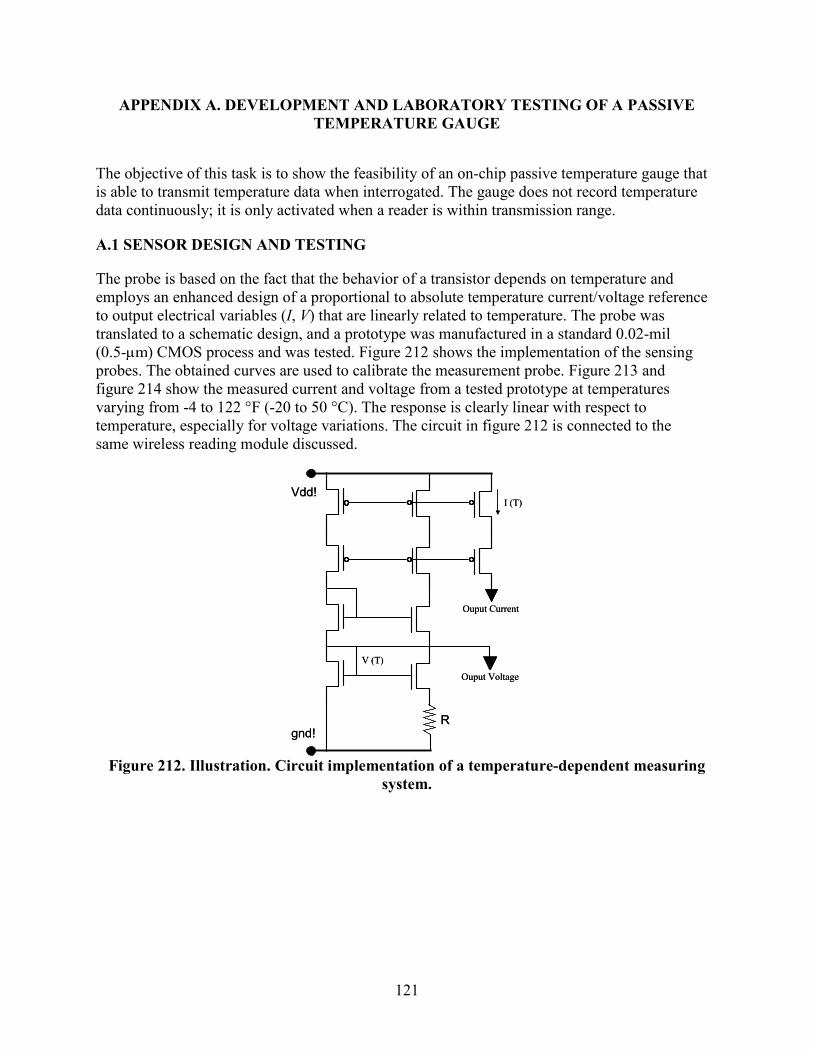
121
APPENDIX A. DEVELOPMENT AND LABORATORY TESTING OF A PASSIVE TEMPERATURE GAUGE
The objective of this task is to show the feasibility of an on-chip passive temperature gauge that is able to transmit temperature data when interrogated. The gauge does not record temperature data continuously; it is only activated when a reader is within transmission range.
A.1 SENSOR DESIGN AND TESTING
The probe is based on the fact that the behavior of a transistor depends on temperature and employs an enhanced design of a proportional to absolute temperature current/voltage reference to output electrical variables (I, V) that are linearly related to temperature. The probe was translated to a schematic design, and a prototype was manufactured in a standard 0.02-mil (0.5-µm ) CMOS process and was tested. Figure 212 shows the implementation of the sensing probes. The obtained curves are used to calibrate the measurement probe. Figure 213 and figure 214 show the measured current and voltage from a tested prototype at temperatures varying from -4 to 122 °F (-20 to 50 °C). The response is clearly linear with respect to temperature, especially for voltage variations. The circuit in figure 212 is connected to the same wireless reading module discussed.
R
Vdd!
gnd!
Ouput Current
Ouput Voltage
I (T)
V (T)
R
Vdd!
gnd!
Ouput Current
Ouput Voltage
I (T)
V (T)
Figure 212. Illustration. Circuit implementation of a temperature-dependent measuring
system.
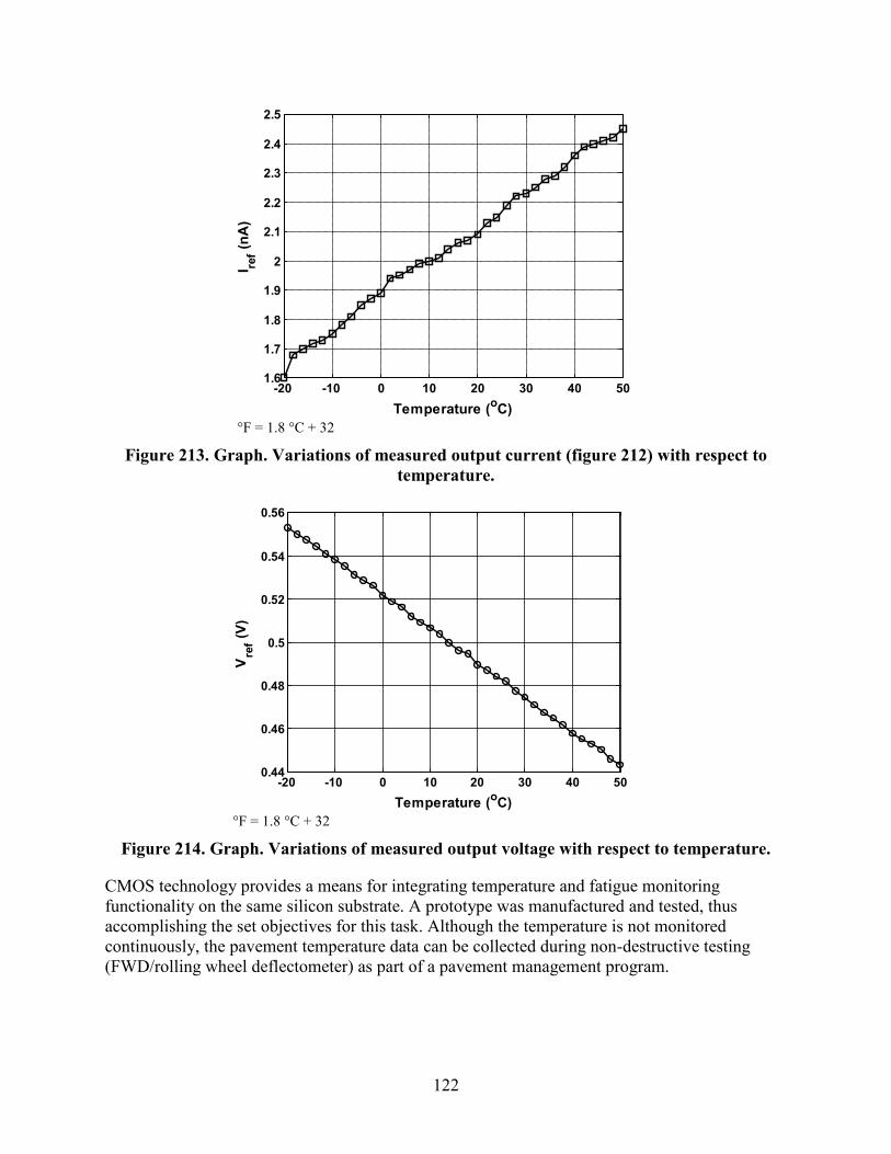
122
-20 -10 0 10 20 30 40 501.6
1.7
1.8
1.9
2
2.1
2.2
2.3
2.4
2.5
Temperature (oC)
I ref (n
A)
°F = 1.8 °C + 32
Figure 213. Graph. Variations of measured output current (figure 212) with respect to temperature.
-20 -10 0 10 20 30 40 500.44
0.46
0.48
0.5
0.52
0.54
0.56
Temperature (oC)
Vre
f (V)
°F = 1.8 °C + 32
Figure 214. Graph. Variations of measured output voltage with respect to temperature.
CMOS technology provides a means for integrating temperature and fatigue monitoring functionality on the same silicon substrate. A prototype was manufactured and tested, thus accomplishing the set objectives for this task. Although the temperature is not monitored continuously, the pavement temperature data can be collected during non-destructive testing (FWD/rolling wheel deflectometer) as part of a pavement management program.

123
APPENDIX B. INTEGRATION AND LABORATORY TESTING OF WIRELESS PROTOCOL WITH OTHER EXISTING INSTRUMENTATION
Researchers studied the feasibility of equipping existing off-the-shelf pressure and humidity sensing systems with RF power-harvesting modules that would alleviate the need for wired power delivery.
B.1 TESTING
A commercial moisture cell was tested in this study. The Dynamax SM200 gauge was selected (see figure 215 and figure 216). The input voltage of the cell was between 5 and 15 V, which allows for powering using a regular 9- or 12-V battery. The output is a voltage signal varying from 0 to 1 V directly proportional to the level of moisture. This format of the output can be integrated with a wireless transmitter. Initial testing was conducted. The main objective was to test the powering scheme of the cell and identify the format of the output. The cell was attached to a 9-V battery, and the output was measured using a commercial multimeter (figure 218). Water was added gradually to a box of sand, and the output voltage was monitored as shown in figure 217. Testing showed that a commercial battery-powered RF module can be used to transmit moisture data.
Figure 215. Photo. Overhead view of Dynamax SM200 moisture gauge.
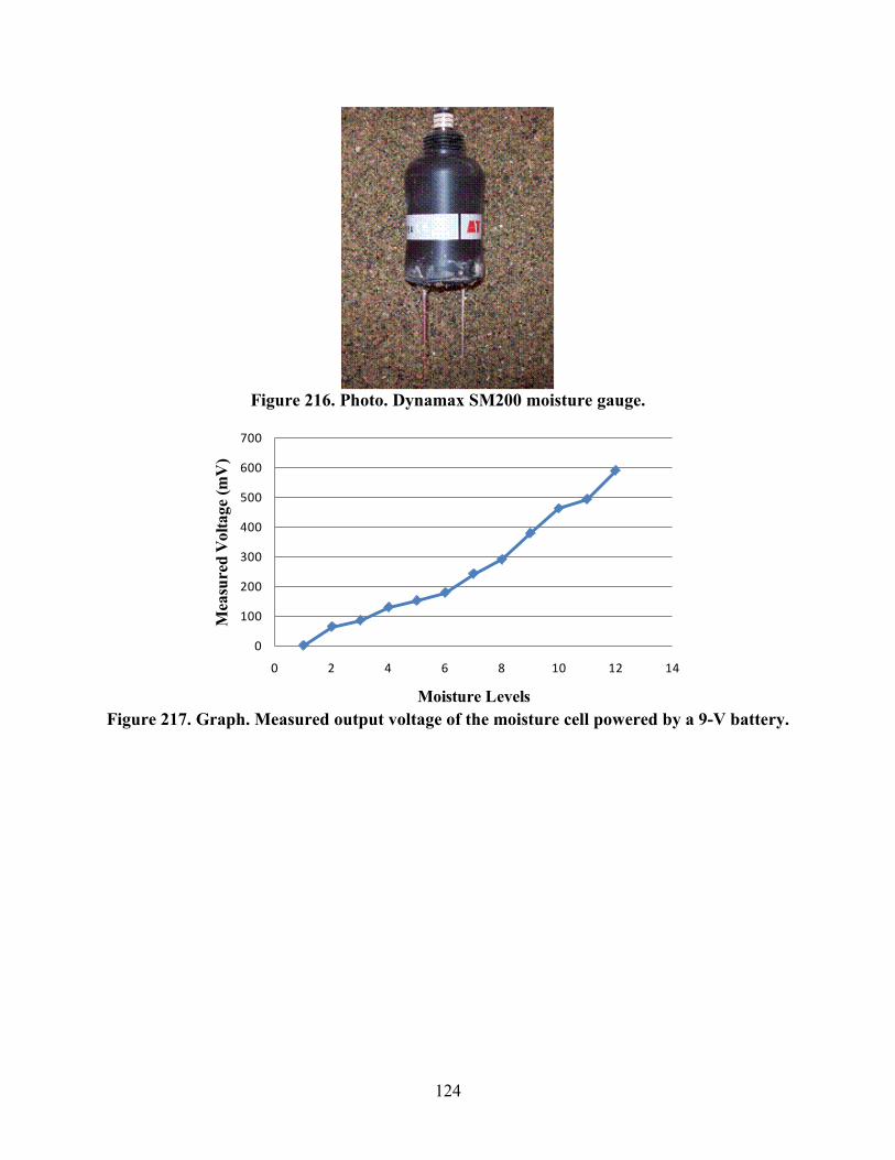
124
Figure 216. Photo. Dynamax SM200 moisture gauge.
0
100
200
300
400
500
600
700
0 2 4 6 8 10 12 14
Mea
sure
d V
olta
ge (m
V)
Moisture Levels Figure 217. Graph. Measured output voltage of the moisture cell powered by a 9-V battery.
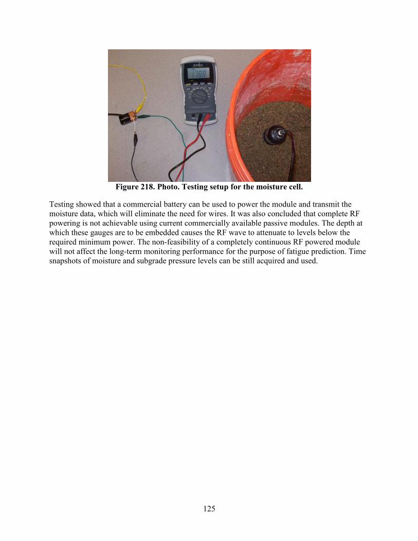
125
Figure 218. Photo. Testing setup for the moisture cell.
Testing showed that a commercial battery can be used to power the module and transmit the moisture data, which will eliminate the need for wires. It was also concluded that complete RF powering is not achievable using current commercially available passive modules. The depth at which these gauges are to be embedded causes the RF wave to attenuate to levels below the required minimum power. The non-feasibility of a completely continuous RF powered module will not affect the long-term monitoring performance for the purpose of fatigue prediction. Time snapshots of moisture and subgrade pressure levels can be still acquired and used.


127
APPENDIX C. DATASHEET AND CALIBRATION CERTIFICATE FOR USED COD GAUGE

128

129
APPENDIX D. DATASHEET FOR USED LVDTS
130

131
REFERENCES
1. Wen, Y., Chen, Y., Li, P., Jiang, D., and Guo, H. (2007). “Smart Concrete with Embedded Piezoelectric Devices: Implementation and Characterization,” Journal of Intelligent Material Systems and Structures, 18(3), 265–274.
2. Fowler, D.W. (1996). “Selection of Bonding Materials for Piezoelectric Sensors,” Proceedings of the National Traffic Data Acquisition Conference, 2, 488, Albuquerque, NM.
3. Hornyak, N.J., Crovetti, J.A., Newman, D.E., and Schabelski, J.P. (2007). Perpetual Pavement Instrumentation for the Marquette Interchange Project-Phase 1, Transportation Research Center, Marquette University, Milwaukee, WI.
4. Roesler, J.R., Scheffy, C.W., Ali, A., and Bush, D. (2000). Construction, Instrumentation, and Testing of Fast-Setting Hydraulic Cement Concrete in Palmdale California, Institute of Transportation Studies, University of California-Berkeley, Berkeley, CA.
5. Timm, D.H., Voller, V.R., Lee, E-B, and Harvey, J. (2001). “Calcool: A Multi-Layer Asphalt Pavement Cooling Tool for Temperature Prediction During Construction,” The International Journal of Pavement Engineering, 2, 169–185.
6. Shah, S.P., Swartz, S.E., and Ouyang, C. (1995). Fracture Mechanics of Concrete: Applications of Fracture Mechanics to Concrete, Rock, and Other Quasi-Brittle Materials, Wiley, New York, NY.
7. Subramaniam, V.K., Edward, F.O., John, S.P., and Surendra, P.S. (2000). “Crack Propagation in Flexural Fatigue of Concrete,” Journal of Engineering Mechanics, 126(9), 891–898.
8. Al-Qadi, I.L. and Walid, N.N. (2003). “Fatigue Shift Factors to Predict HMA Performance,” International Journal of Pavement Engineering, 4(2), 69–76.
9. Wu, R. and Harvey, J.T. (2008). “Evaluation of the Effect of Wander on Rutting Performance in HVS Tests,” Proceedings of the 3d International Conference on Accelerated Pavement Testing, Madrid, Spain.
10. Castell, M.A., Ingraffea, A.R., and Irwin, L.H. (2000). “Fatigue Crack Growth in Pavements,” Journal of Transportation Engineering, 126(4), 283–290.
11. Timm, D. and Priest, A. (2005). Wheel Wander at the NCAT Test Track, NCAT Report 05-02, National Center for Asphalt Technology, Auburn University, Auburn, AL.
12. Chabot, A., Chupin, O., Deloffre, L., and Duhamel, D. (2010). “Viscoroute 2.0: A Tool for the Simulation of Moving Load Effects on Asphalt Pavement,” RMPD Special Issue on Recent Advances in Numerical Simulation of Pavements, 11(2), 227–250.

132
13. Huet, C. (1963). Etude Par Une Méthode d’Impédance Du Comportement Viscoélastique Des Matériaux Hydrocarbons, Ph.D. dissertation, Université de Paris, Paris, France.
14. Huet, C. (1999). “Coupled Size and Boundary-Condition Effects in Viscoelastic Heterogeneous and Composite Bodies,” Mechanics of Materials, 31, 787–829.
15. Sayegh, G. (1995). Contribution à l'étude Des Propriétés Viscoélastiques Des Bitumes Purs Et Des Bétons Bitumineux, Ph.D. dissertation, Faculté des Sciences de Paris, Paris, France.
16. Nilsson, R.N., Hopman, P.C., and Isacsson, U. (2002). “Influence of Different Rheological Models on Predicted Pavement Responses in Flexible Pavements,” Road Materials and Pavement Design, 3(2), 117–147.
17. Chatti, K., Manik, A., Brake, N., Salama, H., and Haider, S.W. (2010). Effect of Michigan Multi-Axle Trucks on Pavement Distress, Report No. RC-1504, Michigan Department of Transportation, Lansing, MI.
18. Violina, B. (2005). “RFID System Components and Costs,” RFID Journal. Obtained from: http://www.rfidjournal.com/article/view/1336.


HRDi-20/05-13(WEB)E