rapid single flux quantum logic - umd physicskosborn/index_files... · rapid single flux quantum...
TRANSCRIPT
Unclassified // For Offical Use Only
15 March 2012
Anna Herr
Rapid Single Flux Quantum Logic
Based on lectures at Chalmers University of Technology, Sweden

Unclassified // For Offical Use Only
2
Fundamental advantages of superconducting digital electronics
• Zero resistance wires 300 GHz interconnects
• Meissner effect Quantum accurate digital bits
• Josephson effect Fast and low energy digital logic
15
0 1007.22
−×≈=Φe
h Wb
sJ
Digital ”1”
0ΦBr
I
S
S 1600 devices2.5 µW at 12 GHz
E = 2 10-19 JV
t
0.5 ps
0.5 mV
Based on lectures at Chalmers University of Technology, Sweden

Unclassified // For Offical Use Only
Digital bits encoded as Single Flux Quanta (SFQ)
3
sJ
Digital ”1”
15
0 1007.22
−×≈=Φe
h Wb
=Φ0 2.07 mVps = 2 mApH0ΦBr
Digital ”0”
Josephson junctions Superconducting state
ϕsin, Cc IIII =<
Voltage stage
dt
dtVII c
ϕπ2
)(, 0Φ=>
Magnetic Flux Quantization
Based on lectures at Chalmers University of Technology, Sweden
Unclassified // For Offical Use Only
4
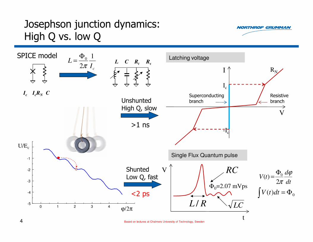
Josephson junction dynamics: High Q vs. low Q
Single Flux Quantum pulse
CIcR
NI
c
∫ Φ= 0)( dttV
cIL
1
2
0
πΦ
=SPICE model
L C Rt
Rs
dt
dtV
ϕπ2
)( 0Φ=
0 1 2 3 4-5
-4
-3
-2
-1
ϕ/2π
U/Ec
I
V
Ic
-Ic
RN
Superconducting branch
Resistive branch
Latching voltage
UnshuntedHigh Q, slow
ShuntedLow Q, fast
LCRL /
RCV
t
>1 ns
<2 psΦ0=2.07 mVps
Based on lectures at Chalmers University of Technology, Sweden
Unclassified // For Offical Use Only
5
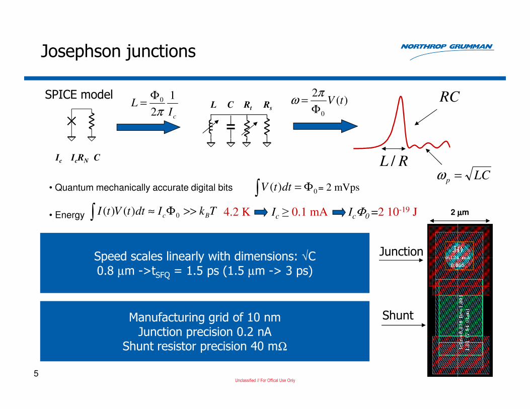
Josephson junctions
• Quantum mechanically accurate digital bits = 2 mVps
• Energy
Junction
Shunt
LCp =ω
L C Rt
Rs
RL /
RC
CIcR
NI
c
∫ Φ= 0)( dttV
TkIdttVtI Bc >>Φ≈∫ 0)()(
cIL
1
2
0
πΦ
= )(2
0
tVΦ
=π
ω
4.2 K Ic ≥ 0.1 mA IcΦ0 =2 10-19 J
Speed scales linearly with dimensions: √C0.8 µm ->tSFQ = 1.5 ps (1.5 µm -> 3 ps)
SPICE model
Manufacturing grid of 10 nmJunction precision 0.2 nA
Shunt resistor precision 40 mΩ
2 µµµµm
Unclassified // For Offical Use Only
6
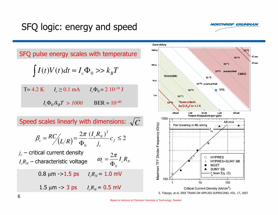
SFQ logic: energy and speed
SFQ pulse energy scales with temperature
TkIdttVtI Bc >>Φ≈∫ 0)()(
T= 4.2 K Ic ≥ 0.1 mA IcΦ0 = 2 10-19 J
IcΦ0 /kBT > 1000 BER = 10-40
Speed scales linearly with dimensions: C
0.8 µm ->1.5 ps IcRN = 1.0 mV
1.5 µm -> 3 ps IcRN = 0.5 mV
( ) 2)(2 2
0
≤Φ
== f
c
Ncc c
j
RI
RLRC π
β
Ncc RI0
2
Φ=
πω
jc – critical current density
IcRN – characteristic voltage
S. Tolpygo, at el, IEEE TRANS ON APPLIED SUPERCOND, VOL. 17, 2007
Based on lectures at Chalmers University of Technology, Sweden
Unclassified // For Offical Use Only
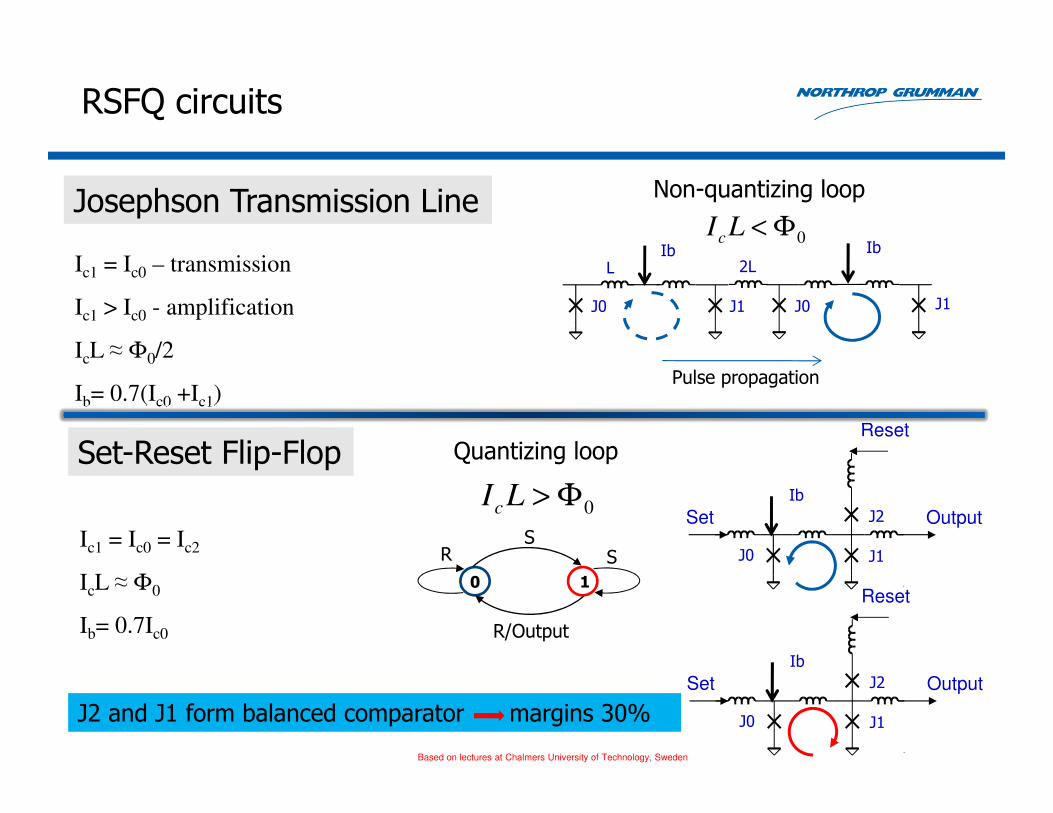
RSFQ circuits
Josephson Transmission Line
J0 J1
0Φ<LIc
Non-quantizing loop
J0
Ib Ib
Pulse propagation
J1
Set-Reset Flip-Flop
Set Output
Reset
J0 J1
J2
Ib
Set Output
Reset
J0 J1
J2
Ib
0Φ>LIc
Quantizing loop
0 1
R/Output
SR S
Ic1 = Ic0 – transmission
Ic1 > Ic0 - amplification
IcL ≈ Φ0/2
Ib= 0.7(Ic0 +Ic1)
L 2L
Ic1 = Ic0 = Ic2
IcL ≈ Φ0
Ib= 0.7Ic0
J2 and J1 form balanced comparator margins 30%
Based on lectures at Chalmers University of Technology, Sweden

Unclassified // For Offical Use Only
RSFQ logic convention
Clock
Data input
”1”
Clock period
Data output
setup time
”1”
Output delay
hold time
Clock period
”0”
A B
Clock Output
XOR (Exclusive Or)
A B XOR
0 0 0
1 0 1
0 1 1
1 1 0
Based on lectures at Chalmers University of Technology, Sweden

Unclassified // For Offical Use Only
9
RSFQ fabrication process and mask layout
0.8 µµµµm0.45 µµµµm
wira (M2)
gnde (M0)
dm
w
Superconductive inductor over ground plane
wira (M2)
Ground plane
• Localized field
• Inductance is per square
• Negligible crosstalk
• Negligible losses
• Scales with feature size
Nb
SiO2
Based on lectures at Chalmers University of Technology, Sweden

Unclassified // For Offical Use Only
• High speed up to 750 GHz for single asynchronous cells and up to 200 GHz for LSI devices
• Low power consumption 0.2 nW/GHz per pulse
• Superconducting microstrip lines for ballistic transfer ofdata over arbitrary distances
• Complete library of digital gates
• Simple fabrication technology
• Operational temperature < 10K.Prof. V.K. Semenov
Prof. K.K. Likharev
RSFQ logic/memory family
Dr. O.A. Mukhanov
RSFQ logic/memory family: a new Josephson-junction technology for sub-terahertz-clock-frequency digital systems
IEEE Trans. On Applied Supercond, Vol. 1, No. 1, 1991
Based on lectures at Chalmers University of Technology, Sweden

Unclassified // For Offical Use Only
Applications: Power, speed, accuracy, operating temperature
11
Device Junction count Application
A/D and D/A converters 104 Radar and telecommunication
Digital Signal Processing 106 Radar and telecommunication
Digital SQUID 104 Biomagnetic applications, nondestructive evaluation
Readout for large array of sensors 104 Radio astronomy, material science
Time-digital converters 103 High-energy and nuclear physics
Digital Correlator 104 Radio astronomy
General purpose microprocessor >>106 Supercomputing
Control for qubit 103 Quantum computing
Based on lectures at Chalmers University of Technology, Sweden

Unclassified // For Offical Use Only
RSFQ progress
• Japan: governmental project over 6 years with 50 M$ budget
– 2005: 10 metallization layer process
– 2006: demonstration of the microprocessor
– 2007: cryocooler packaged prototype of the packet switch
• USA: military contracts at Hypres Inc.
– 2005: cryocooler packaged prototype of the Ka-band digital receiver
– 2006: cryocooler packaged prototype of the X-band digital receiver
– 2007: demonstration at ARMY and AIR FORCE facilities
• USA: military contracts at Northrop Grumman Inc.
– 2002: demonstration of the 60 Gbps chip-to-chip communication
– 2006: demonstration of the 10 Gbps output link
– 2007: break through on the second order ADCs
• Europe: Swedish national and EU projects at Chalmers University
– 2005: demonstration of Digital Signal Processor components
– 2007: assembling of the cryocooler based DSP system
12Based on lectures at Chalmers University of Technology, Sweden

Unclassified // For Offical Use Only
Scaling to VLSI circuits is challenging
13
• High static power dissipation
• Power applied in parallel
• High overhead in Josephson junctions for clock distribution
10-4
10-3
10-2
10-1
100
100
101
102
103
104
105
106
107
Gate
Pow
er
/ k
BT
Activity Factor
CryoCMOS
RSFQ
Ebit=1000 kbT
Based on lectures at Chalmers University of Technology, Sweden

Unclassified // For Offical Use Only
14
RSFQ power supply
DC power
Rshunt
Rbias
Rbias > 5 Rshunt
Vbias ≈ 5 mV (1.5 µm 2.6 mV)
Pstatic ≈ 0.5 mW/JJ
DC power: increase in speed gives increase in static power dissipation
DC power3 µµµµm 90 mA
10x power dissipated in bias resistors than in Josephson junctions
Bias resistor
High stray magnetic field
Nonuniform ground currents
High heat load
Gates are biased in parallel: power network is a large current divider
Biasing 10,000 JJs requires 1 A of current
Superconducting shield (SuShi)
Superconducting shield
Multiple bias lines
Current recycling
Based on lectures at Chalmers University of Technology, Sweden

Unclassified // For Offical Use Only
Clock
Data input
”1” ”1”
Clock period
Data output
setup time
”1”
delay
hold time
jitter jitter
9σσσσ
• thermal noise and fab spread related jitter• timings depend on state • timings depend on speed• timings depend on the state of the
neighboring cells
RSFQ timing
Local clocks accumulate thermal noise and data dependent skews
0 2 4 6 8 10 12 14 16 18 20-30
-25
-20
-15
-10
-5
0
5
Data Data
Clock
DC power
J0 J1
J2
J3
State 0
State 1
DC bias current determines slope of washboard
Based on lectures at Chalmers University of Technology, Sweden

Unclassified // For Offical Use OnlyBased on lectures at Chalmers University of Technology, Sweden
• 80 % overhead in Josephson junctions for clock distribution
• 1 A of bias currents
• accumulated jitter
• Extra junctions for separation of a clock like from the gates
• Extra junctions for adjustments of the delays between gates
Data dependent timing parameters

Unclassified // For Offical Use Only
+ + + +
+ + + +
sum
carry
clock
+ + + +
+ + + +
sum
carry
clock
sum
carry
clock
Clock skew
∆∆∆∆T
Clock
+ + + +
+ + + +
+ + + +
+ + + +
sum
carry
FIFO FIFO FIFO
FIFO FIFO FIFO
clock
clock
Large parallel circuits requires active synchronization
• Active synchronization adds even more junctions
• Global reset is needed to recover state of FIFOs
9σ ≈ 1.5 ps Tclock = 50 ps 1000 junctions in clock lines
Based on lectures at Chalmers University of Technology, Sweden
Unclassified // For Offical Use Only
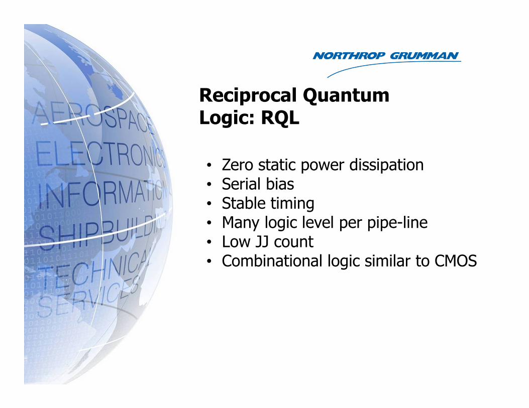
Reciprocal Quantum Logic: RQL
• Zero static power dissipation• Serial bias• Stable timing• Many logic level per pipe-line• Low JJ count• Combinational logic similar to CMOS
Unclassified // For Offical Use Only
191919
AC power
A
RQL Power
A
1 1 0
LIC
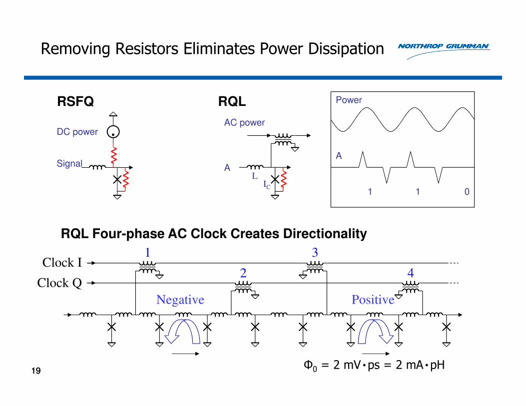
Removing Resistors Eliminates Power Dissipation
Signal
RSFQ
DC power
1
PositiveNegative
Ф0 = 2 mV٠ps = 2 mA٠pH
RQL Four-phase AC Clock Creates Directionality
Clock I
Clock Q
3
2 4

Unclassified // For Offical Use Only
20
RQL Logic Gate Schematics are Simple Like CMOS
CLK
MVTL CMOS
RSFQ
A
B
A
BAND
OR
A
B
A
B
AND
OR
A
BA
B
AND
OR
CLK
Critical current margins > 50%
RQL
AND
OR
A B
Power/Clock
First input goes to
OR. Second input
goes to AND

Unclassified // For Offical Use Only
215 mm
Adder logic:
• 8 bits• 1.25 clock latency• 50 logic gates, 240 JTLs• 800 Josephson junctions• < 1 µW power
Power splitters:
• 8 way Wilkinson splitters• 2-12 GHz clock rate• Bias current 2 mA/per line
Output amplifiers:
• Distributed output amplifiers• 2 mV up to 10 GHz
Hypres 4500 process
1647 total JJs
RQL Carry Look-Ahead Adder has been designed using CMOS-like logic synthesis

Unclassified // For Offical Use Only
RQL is low power and scalable
=
RSFQ JTL RQL CLA
2.6 mV0.200 mA
= 500 nW
RQL pulse: 0.3 ICФ0f = 0.3 nW for 0.1 mA junction at 6 GHz
AC power: 6 mW for 15 mA on a 50 Ohm line
Factor of20,000,000
22
RQL is 10x better than CMOS in 300WPower Gates Clock frequency Computational power
CMOS 45 nm
300 W 90M/chip 1 GHz 1017 gates/s
RQL 1 µm (0.1mA)
50 mW (300 W wall plug) 50M/MCM 20 GHz 1018 gates/s

Unclassified // For Offical Use Only
Conclusion
300 GHz interconnects Quantum accurate bits SFQ logic
sJ
Digital ”1”
0ΦBr
1600 devices2.5 µW at 12 GHz
E = 2 10-19 JV
t
0.5 ps
0.5 mV
SFQ logic is fast and with small signal power
High maturity level: applications, fabrication, packaging, design
Reversible logic provides path to lower power dissipation
Based on lectures at Chalmers University of Technology, Sweden
500 nW
RQL