rao pahald singh group of institutions balana(mohinder garh)123029 lab manual.pdf · ·...
TRANSCRIPT

1 Analog Electronics Lab (EE-222-F)
Analog Electronics Lab
(EE-222-F)
LAB MANUAL
IV SEMESTER
RAO PAHALD SINGH GROUP OF INSTITUTIONS
BALANA(MOHINDER GARH)123029
Department Of Electronics and Communication Engg.
RPS CET, Balana(M/Garh)

2 Analog Electronics Lab (EE-222-F)
LIST OF EXPERIMENTS
S.NO. NAME OF THE EXPERIMENT Page
1 To get familiar with working knowledge of the following instruments. (a)
CRO (b) multimeter (c) function generator (d) regulated power supply (e)
active passive components (f) bread board.
2 Study of V-I Characteristics of a Diode.
3 To study and draw the characteristics of half wave and full wave rectifiers.
4 To study zener diode characteristics.
5 To study zener diode as voltage regulator.
6 To study and draw the characteristics of FET in common source configuration.
7 To study and draw the characteristics of SCR.
8 To study and draw the characteristics of DIAC.
9 To plot V-I characteristic of TRIAC.
10 To study and draw the characteristics of FET in common drain configuration.

3 Analog Electronics Lab (EE-222-F)
EXPERIMENT NO. 1
AIM: To get familiar with working knowledge of the following instruments.
THEORETICAL CONCEPT:
A. CATHODE RAY OSCILLOSCOPE:
The cathode-ray oscilloscope (CRO) is a common laboratory instrument that provides accurate time and amplitude measurements of voltage signals over a wide range of frequencies. Its
reliability, stability, and ease of operation make it suitable as a general purpose laboratory instrument. The heart of the C RO is a cathode-ray tube shown schematically in Fig. 1.
The cathode ray is a beam of electron s which are emitted by the heated cathode (Negative electrode) and accelerated toward the fluorescent screen. The assembly of the cathode, intensity
grid, focus grid, and accelerating anode (positive electrode) is called an electron gun. Its purpose is to generate the electron beam and control its intensity and focus between the electron gun and
the fluorescent screen are two pair of metal plates - one oriented to provide horizontal deflection of the beam and one pair oriented to give vertical deflection to the beam. These plates are thus
referred to as the horizontal and vertical deflection plates. The combination of these two
deflections allows the beam to reach any portion of the fluorescent screen. Wherever the electron beam hits the screen, the phosphor is excited and light is emitted from that point. This conversion
of electron energy into light allows us to write with points or lines of light on an otherwise darkened screen. In the most common use of the oscilloscope the signal to be studied is first
amplified and then applied to the vertical (deflection) plates to deflect the beam vertically and at the same time a voltage that increases linearly with time is applied to the horizontal (deflection)
plates thus causing the beam to be deflected horizontally at a uniform (constant rate). The signal applied to the vertical plates is thus displayed on the screen as a function of time. The horizontal
axis serves as a uniform time scale. The linear deflection or sweep of the beam horizontally is
accomplished by use of a sweep generator that is incorporated in the oscilloscope circuitry. The voltage output of such a generator is that of a saw tooth wave as shown in Fig. 2. application of
one cycle of this voltage difference, which increases linearly with time, to the horizontal plates causes the beam to be deflected linearly with time across the tube face. When the voltage

4 Analog Electronics Lab (EE-222-F)
suddenly falls to zero, as at points (a) (b) (c), etc...., the end of each sweep - the beam flies back to its initial position. The horizontal deflection of the beam is repeated periodically, the frequency of
this periodicity is adjustable by external controls.
To obtain steady traces on the tube face, an internal number of cycles of the unknown signal that
is applied to the vertical plates must be associated with each cycle of the sweep generator. Thus,
with such a matching of synchronization of the two deflections, the pattern on the tube face
repeats itself and hence appears to remain stationary. The persistence of vision in the human eye
and of the glow of the fluorescent screen aids in producing a stationary pattern. In addition,
the electron beam is cut off (blanked) during fly back so that the retrace sweep is not observed.
B. THE MULTIMETER STRUCTURE:
A multimeter is used to make various electrical measurements, such as AC and DC voltage, AC
and DC current, and resistance. It is called a multimeter because it combines the functions of a
voltmeter, ammeter, and ohmmeter. Multimeters may also have other functions, such as diode
and continuity tests. The descriptions and pictures that follow are specific to the fluke 73 Series
III multimeter, but other multimeters are similar.
Important note: The most common mistake when using a multimeter is not switching the test
leads when switching between current sensing and any other type of sensing (voltage,
resistance). It is critical that the test leads be in the proper jacks for the measurement you are
making.
Safety Information • Be sure the test leads and rotary switch are in the correct position for the desired
measurement. • Never use the meter if the meter or the test leads look damaged. • Never measure resistance in a circuit when power is applied. • Never touch the probes to a voltage source when a test lead is plugged into the 10 A or 300
mA input jack.

5 Analog Electronics Lab (EE-222-F)
• To avoid damage or injury, never use the meter on circuits that exceed 4800 watts. • Never apply more than the rated voltage between any input jack and earth ground (600 V for
the Fluke 73). • Be careful when working with voltages above 60 V DC or 30 V AC rms. Such voltages pose a
shock hazard. • Keep your fingers behind the finger guards on the test probes when making measurements. • To avoid false readings, which could lead to possible electric shock or personal injury, replace
the battery as soon as the battery indicator appears.
B. FUNCTION GENERATOR:
A function generator is a device that can produce various patterns of voltage at a variety of
frequencies and amplitudes. It is used to test the response of circuits to common input signals.
The electrical leads from the device are attached to the ground and signal input terminals of the
device under test.
Features and controls • Most function generators allow the user to choose the shape of the output from a small
number of options.
• Square wave - the signal goes directly from high to low voltage. Sine wave - the
signal curves like a sinusoid from high to low voltage. Triangle wave - the signal
goes from high to low voltage at a fixed rate.
• The amplitude control on a function generator varies the voltage difference between
the high and low voltage of the output signal. • The direct current (DC) offset control on a function generator varies the average
voltage of a signal relative to the ground. • The frequency control of a function generator controls the rate at which output signal
oscillates. On some function generators, the frequency control is a combination of
different controls. • One set of controls chooses the broad frequency range (order of magnitude) and the
other selects the precise frequency. This allows the function generator to handle the
enormous variation in frequency scale needed for signals.

6 Analog Electronics Lab (EE-222-F)
How to use a function generator?
• After powering on the function generator, the output signal needs to be configured to
the desired shape. Typically, this means connecting the signal and ground leads to an
oscilloscope to check the controls. • Adjust the function generator until the output signal is correct, then attach the signal
and ground leads from the function generator to the input and ground of the device
under test. • For some applications, the negative lead of the function generator should attach to
negative input of the device, but usually attaching to ground is sufficient.
Conclusions:
• A function generator is a device that can produce various patterns of voltage at a
variety of frequencies and amplitudes.
D. REGULATED POWER SUPPLY
Types of Power Supply There are many types of power supply. Most are designed to convert high voltage AC mains
electricity to a suitable low voltage supply for electronic circuits and other devices. A power supply can by broken down into a series of blocks, each of which performs a particular
function.
For example a 5V regulated supply:
Each of the blocks is described in more detail below: • Transformer - steps down high voltage AC mains to low voltage AC. • Rectifier - converts AC to DC, but the DC output is varying. • Smoothing - smoothes the DC from varying greatly to a small ripple. • Regulator - eliminates ripple by setting DC output to a fixed voltage
POWER: Push button switches for supplying power to instrument.
OUTPUT ON:
Push button for switching (ON / OFF) the three output voltages. 3 and 6 V/mA (Push button):
Switch the display from voltage in to current reading or vice versa. When push buttons are
pressed, the current supplied from the terminals 12 and 17 is displayed with a resolution of 1 mA. In released position voltages across the terminals 12 and 17 are displayed with a
resolution of 0.1 V.

7 Analog Electronics Lab (EE-222-F)
4 AND 7 DIGITAL DISPLAYS (7-Segment LED): Digital display with 3-digit readout for output voltage and current. On the left side of the
instrument the voltage and current readings for terminals 3 is indicated. The corresponding
values for the terminals 4 are indicated on the right side of the display.
5V AND 8V INDICATORS: Two LEDs indicate the unit of the display. The mA LED flashes when the 0 – 30V DC output
is used in constant current mode, or output current required is in excess of specified value, in
CV mode. E. ACTIVE, PASSIVE COMPONENTS
An electronic component is a basic electronic element and may be available in a discrete form (a discrete device or discrete component) having two or more electrical terminals (or leads). These are intended to be connected together, usually by soldering to a printed circuit board, in order to create an electronic circuit and a discrete circuit with a particular function (for example an amplifier, radio receiver, or oscillator). Basic electronic components may be packaged discretely, as arrays or networks of like components, or integrated inside of packages such as semiconductor integrated circuits, hybrid integrated circuits, or thick film devices.
A component may be classified as passive or active. The strict physics definition treats passive
components as ones that cannot supply energy themselves; whereas a battery would be seen as an
active component since it truly acts as a source of energy.
Passive components are ones which cannot introduce net energy into the circuit they are

8 Analog Electronics Lab (EE-222-F)
connected to. They also cannot rely on a source of power except for what is available from the (AC) circuit they are connected to. As a consequence they are unable to amplify (increase the power of a signal); although they may well increase a voltage or current such as is done by a transformer or resonant circuit. Among passive components are familiar two-terminal components such as resistors, capacitors, inductors, and transformers. Active components rely on a source of energy (usually from the DC circuit, which we have chosen to ignore) and are usually able to inject power into a circuit although this is not part of the definition. This includes amplifying components such as transistors, triode vacuum tubes (valves), and tunnel diodes.
Passive components can be further divided into lossless and lossy components:
Lossless components do not have a net power flow into or out of the component. This would
include ideal capacitors, inductors, transformers, and the (theoretical) gyrator. Lossy or dissipative components do not have that property and generally absorb power from the external circuit over time. The prototypical example is the resistor. In practice all non-ideal passive components are at least a little lossy, but these are typically modeled in circuit analysis as consisting of an ideal lossless component with an attached resistor to account for the loss. Most passive components with more than two terminals can be described in terms of two-port parameters satisfying the principle of reciprocity, although there are some rare exceptions
In
contrast, active components (which have more than two terminals) generally lack that property. Note that these distinctions only apply to components listed below which would be modeled as elements within circuit analysis. Practical items which act as transducers or have other connections to the outside world such as switches cannot be subject to this form of classification since they defy the view of the electronic circuit as a closed system.
F. BREAD BOARD
A breadboard is used to build and test circuits quickly before finalizing any circuit design. The
breadboard has many holes into which circuit components like ICs and resistors can be inserted.
A typical breadboard is shown below:
The bread board has strips of metal which run underneath the board and connect the holes on the
top of the board. The metal strips are laid out as shown below. Note that the top and bottom rows
of holes are connected horizontally while the remaining holes are connected vertically.
9 Analog Electronics Lab (EE-222-F)
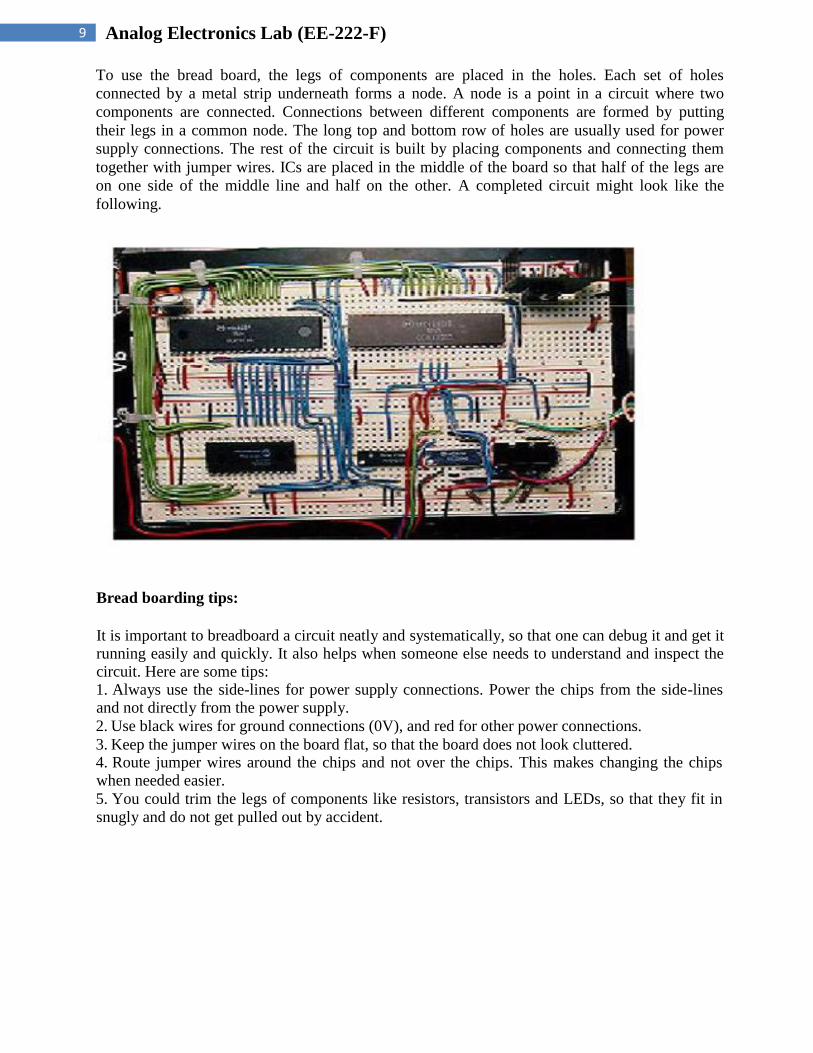
To use the bread board, the legs of components are placed in the holes. Each set of holes
connected by a metal strip underneath forms a node. A node is a point in a circuit where two
components are connected. Connections between different components are formed by putting
their legs in a common node. The long top and bottom row of holes are usually used for power
supply connections. The rest of the circuit is built by placing components and connecting them
together with jumper wires. ICs are placed in the middle of the board so that half of the legs are
on one side of the middle line and half on the other. A completed circuit might look like the
following.
Bread boarding tips:
It is important to breadboard a circuit neatly and systematically, so that one can debug it and get it running easily and quickly. It also helps when someone else needs to understand and inspect the circuit. Here are some tips: 1. Always use the side-lines for power supply connections. Power the chips from the side-lines and not directly from the power supply.
2. Use black wires for ground connections (0V), and red for other power connections. 3. Keep the jumper wires on the board flat, so that the board does not look cluttered. 4. Route jumper wires around the chips and not over the chips. This makes changing the chips when needed easier. 5. You could trim the legs of components like resistors, transistors and LEDs, so that they fit in
snugly and do not get pulled out by accident.

10 Analog Electronics Lab (EE-222-F)
EXPERIMENT NO. 2
AIM: To study of V-I characteristics of a diode.
THEORETICAL CONCEPT: A P-N junction is known as Semiconductor diode or crystal
diode. It is the combination of P-type and N-type Semiconductor. This offers nearly zero
resistance to current on forward biasing and nearly infinite Resistance to the flow of current when
in revere biased.
Forward biasing: When P-type semiconductor is connected to the +ve terminal and N-type to –
ve terminal of voltage source. Nearly zero resistance is offered to the flow of current.
Reverse biasing: When P-type semiconductor is connected to the –ve terminal and N-type to +ve
terminal. Nearly zero current flow in this condition. EXPERIMENTAL SET UP:
(1) When diode is forward biased
(2) When diode is reverse biased
SPECIFICATION OF APPARATUS USED: Diode characteristics kit, power supply, ammeter
(0-20mA), voltmeter (0-20V) and connecting leads.

11 Analog Electronics Lab (EE-222-F)
PROCEDURE:
(1) Connect the circuit as shown in fig.
(2) Switch on the power supply.
(3) Vary the value of input dc supply in steps.
(4) Note down the ammeter and voltmeter readings for each step.
(5) Plot the graph of voltage and current.
(6) Connect the circuit as shown in fig.
PRECAUTIONS:
(1) Always connect the voltmeter in parallel and ammeter in series as shown in fig.
(2) Connection should be proper and tight.
(3) Switch ‘ON’ the supply after completing the circuit.
(4) DC supply should be increased slowly in steps.
(5) Reading of voltmeter and ammeter should be accurate.
OBSERVATION DATA:
GRAPH:

12 Analog Electronics Lab (EE-222-F)
RESULT AND COMMENTS: The graph has been plotted between voltage and current. The
diode doesn’t conduct in reverse bias state and conduct in forward bias state.

13 Analog Electronics Lab (EE-222-F)
EXPERIMENT NO. 3
AIM: To study and draw the characteristics of half wave and full wave rectifiers.
THEORETICAL CONCEPT: Rectification is a process of conversion of AC to DC. In half-
wave rectifier, only one diode is used. During +ve half cycle the diode is forward biased and it
conducts current through the load resistor R .During –ve half cycle diode is reverse biased Hence,
no current flow through the circuit. Only +ve half cycle appears across the load, whereas, the –ve
half cycle is suppressed.
Full Wave Rectifier: In full-wave rectifier, when AC supplied at the input, both the half cycle
current flows through the load in the same direction. The following two circuits are commonly
employed.
Centre-tap full-wave Rectifier: In this rectifier two diode and a center-tap transformer is used.
During +ve half cycle the diode D1 is forward biased and D2 is reverse biased. Output will be
obtained across load resistor R. During –ve half cycle diode D1 is reverse biased andD2 is
forward biased. Output will be obtained cross load resistor R and the direction of output is same
i.e., DC output is obtained.
Bridge Rectifier: The circuit contains four diodes connected to form a bridge. In this an ordinary
transformer is used. During +ve half cycle of secondary voltage, diodes D1 and D3 are forward
biased and diodes D2 and D4 are reverse biased and vice versa.
EXPERIMENTAL SET UP:-
HALF WAVE RECTIFIER

14 Analog Electronics Lab (EE-222-F)
FULL WAVE RECTIFIER
SPECIFICATION OF APPARATUS USED: Power supply, rectifier kit, CRO, connecting
leads.
PROCEDURE:
1. Connect the circuit as per the circuit diagram
2. The output is noted down on CRO.
3. Graph is drawn by noting down peak to peak amplitude of input and output voltage.
PRECAUTIONS:
1. Connections should be tight
2. Handle the equipments with care.
OBSERVATION DATA:

15 Analog Electronics Lab (EE-222-F)
GRAPH:
Half wave rectifier
Full wave rectifier
RESULT AND COMMENTS: Waveforms of full wave and half wave rectifier have drawn.

16 Analog Electronics Lab (EE-222-F)
EXPERIMENT NO. 4
AIM: To study zener diode characteristics.
THEORETICAL CONCEPT:-An ideal P-N Junction diode does not conduct in reverse biased
condition. A zener diode conducts excellently even in reverse biased condition. These diodes
operate at a precise value of voltage called break down voltage. A zener diode when forward
biased behaves like an ordinary P-N junction diode. A zener diode when reverse biased can either
undergo avalanche breakdown or zener breakdown.
Avalanche break down:-If both p-side and n-side of the diode are lightly doped, depletion region
at the junction widens. Application of a very large electric field at the junction may rupture
covalent bonding between electrons. Such rupture leads to the generation of a large number of
charge carriers resulting in avalanche multiplication.
Zener break down:-If both p-side and n-side of the diode are heavily doped, depletion region at
the junction reduces. Application of even a small voltage at the junction ruptures covalent
bonding and generates large number of charge carriers. Such sudden increase in the number of
charge carriers results in zener mechanism.
EXPERIMENTAL SET UP:-

17 Analog Electronics Lab (EE-222-F)
SPECIFICATION OF APPARATUS USED:-Regulated DC power supply, voltmeter,
connecting wires, kit
Specifications:
Breakdown Voltage = 5.1V
Power dissipation = 0.75W
Max. Forward Current = 1A
PROCEDURE:
Forward biased condition:
1. Connect the circuit as shown in fig (1).
2. Vary Vzf gradually and note down the corresponding readings of Izf.
3. Step size is not fixed because of non linear curve and vary the X-axis variable (i.e. if
output variation is more, decrease input step size and vice versa).
4. Tabulate different forward currents obtained for different forward voltages.
Reverse biased condition:
1. Connect the circuit as shown in fig (2).
2. Vary Vzr gradually and note down the corresponding readings of Izr.
3. Step Size is not fixed because of non linear curve and vary the X-axis variable (i.e. if
output variation is more, decrease input step size and vice versa).
4. Tabulate different reverse currents obtained for different reverse voltages.
PRECAUTIONS:
1. While doing the experiment do not exceed the ratings of the diode. This may lead to
damage the diode.
2. Connect voltmeter and Ammeter in correct polarities as shown in the circuit diagram.
3. Does not switch ON the power supply unless you have checked the circuit
connections as per the circuit diagram.

18 Analog Electronics Lab (EE-222-F)
OBSERVATIONS DATA:
Zener diode in forward bias:
Sr. No. Forward voltage across the diode
(Vzf) Forward current across the diode
(Izf)
Zener diode in Reverse bias:
Sr. No. Reverse voltage across the diode
(Vzr) Reverse current across the diode
(Izr)
GRAPH:
CALCULATIONS FROM GRAPH:
Static forward resistance Rdc = Vf /If
Dynamic forward resistance rac = ΔVf /ΔIf
Static reverse resistance Rdc = Vr/Ir
Dynamic reverse resistance rac = ΔVr /ΔIr

19 Analog Electronics Lab (EE-222-F)
RESULT AND COMMENTS:-
1. The zener diode characteristics have been studied.
2. The zener resistance at the breakdown voltage was found to be = ………

20 Analog Electronics Lab (EE-222-F)
EXPERIMENT NO. 5
AIM: To study zener diode as voltage regulator.
THEORETICAL CONCEPT: The zener diode is operated in the breakdown or zener region,
the voltage across it is substantially constant for a large current of current through it. This
characteristic permits it to be used as a voltage regulator. As the lode current increases, the Zener
current decrease so that current through resistance Rs is constant. As output voltage = Vin – Irs,
and I is constant, Therefore, output Voltage remains unchanged. The input voltage Vin increase,
more current will flow through the zener, the voltage drop across Rs will increase but lode voltage
would remain constant.
EXPERIMENTAL SET UP:-
SPECIFICATION OF APPARATUS USED: Power supply, zener diode, two voltmeter and
connected leads ammeter.
PROCEDURE:
(a) Connect the circuit as per the circuit diagram.
(b) Keep load resistance constant (take maximum value of load resistance)
(c) Vary input voltage and note down output voltage.
(d) Now keep input voltage constant and vary load resistance and note down
corresponding voltmeter reading.
(e) Plot the respective graph.
PRECAUTIONS:
(a) Connections should be tight.
(b) Handle the equipments with care.

21 Analog Electronics Lab (EE-222-F)
OBSERVATION DATA:
S. No Vs( VOLT) V( VOLT) RL(E) V (VOLT)
RESULT AND COMMENTS: Studied how zener diode is used as a voltage regulator.

22 Analog Electronics Lab (EE-222-F)
EXPERIMENT NO. 6
AIM: To study and draw the characteristics of FET in common source configuration.
THEORETICAL CONCEPT:-A FET is a three terminal semiconductor device in which current
conduction is by one type of carries and is controlled by the effect of electric field. There are two
types of FET namely JFET and MOSFET. Again, a JFET can either have N-channel or P-channel.
A N-channel JFET has a N-type semiconductor bar, the two ends of which make the Drain and
source terminal. On the two sides of this bar, P-N junction is made. This P region makes gate.
Usually, these two gates are connected Together to form a single gate .The gate is given a –ve
bias with respect to source. The drain is given +ve potential with respect to source.
EXPERIMENTAL SET UP:-
SPECIFICATION OF APPARATUS USED: Power supply, FET characteristic Kit, connecting
leads, two multimeters.
PROCEDURE:
Input characteristics:
(a)Connect the circuit as per the circuit diagram
(b)Keep drain-source voltage constant
(c)Vary gate-source voltage in steps and note down drain current
(d) Readings are tabulated and graph is drawn
Output characteristics
(a)Keep gate-source voltage constant
(b)Vary drain-source voltage in steps and note down drain current.
(c) Readings are tabulated and graph is drawn.
PRECAUTIONS: (a)Connections should be tight.
(b)Handle the equipments with care.

23 Analog Electronics Lab (EE-222-F)
OBSERVATION TABLE:
S. No
I/P at const. VDS O/P at const. VGS
VGS (V) ID (mA) VDS ( V) ID (mA)
1
2
3
4
5
6
7
8
9
10
GRAPH:
Input characteristics:

24 Analog Electronics Lab (EE-222-F)
Output characteristics:
RESULT AND COMMENTS: Input and output characteristics is obtained.
25 Analog Electronics Lab (EE-222-F)
EXPERIMENT NO. 7
AIM: To study and draw the characteristics of SCR.
THEORETICAL CONCEPT: Silicon control rectifier (SCR) is a four layer, three terminal
semiconductor devices, the end ‘P’ forms the anode and the end ‘N’ forms the cathode and the
gate terminal ‘G’ is from the ‘P’ layer next to cathode. It is a unidirectional device. The device
can exist upon either ON state or OFF state depending upon the applied voltage. When anode
voltage is +ve with respect to cathode the SCR start conducting. If some small gate voltage is
applied, the SCR trigger at some low value of anode voltage, but it loses its all control on the SCR
current after triggering. Therefore, in order to turn the SCR to OFF position the anode voltage to
be reduced to zero.
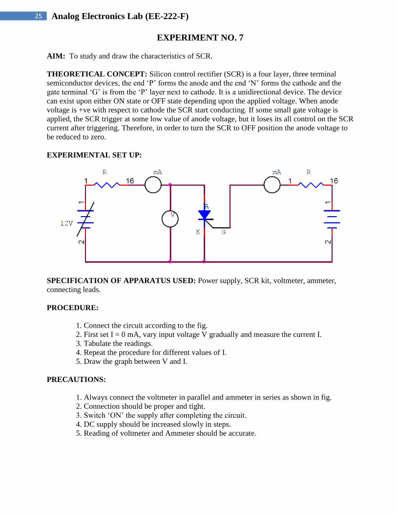
EXPERIMENTAL SET UP:
SPECIFICATION OF APPARATUS USED: Power supply, SCR kit, voltmeter, ammeter,
connecting leads.
PROCEDURE:
1. Connect the circuit according to the fig.
2. First set I = 0 mA, vary input voltage V gradually and measure the current I.
3. Tabulate the readings.
4. Repeat the procedure for different values of I.
5. Draw the graph between V and I.
PRECAUTIONS:
1. Always connect the voltmeter in parallel and ammeter in series as shown in fig.
2. Connection should be proper and tight.
3. Switch ‘ON’ the supply after completing the circuit.
4. DC supply should be increased slowly in steps.
5. Reading of voltmeter and Ammeter should be accurate.

26 Analog Electronics Lab (EE-222-F)
OBSERVATION DATA:
Sr.
No.
VAK(Volt) IAK(mA)
1
2
3
4
5
GRAPH:
SCR Characteristics
RESULT AND COMMENTS: The characteristics of thyristor have been plotted. The SCR will
not conduct until it is not triggered by gate voltage.

27 Analog Electronics Lab (EE-222-F)
EXPERIMENT NO. 8
AIM: To study and draw the characteristics of DIAC.
THEORETICAL CONCEPT:
Diac: A Diac is a two terminal and four layer bi-directional semiconductor switching device. ‘Di
means two (two terminal device) and ‘ac’ means alternating current hence diac is a switch. In fact,
it is a device which can conduct in both the directions only when the applied voltage is more than
its break over voltage. It is similar as if two latches are connected in parallel. During +ve half-
cycle, the right four layer diode conducts heavily. During –ve half-cycle, the left diode conducts
heavily only when the supply voltage exceeds the break over voltage of the Diac.
Circuit for DIAC
SPECIFICATION OF APPARATUS USED: Power supply, Diac characteristic, connecting
leads, ammeter and voltmeter.
PROCEDURE:
1. Make connection as per circuit diagram.
2. Apply +ve supply to the circuit.
3. Increase the voltage step by step and note down the corresponding current values.
4. After a certain voltage, the diac enter in –ve resistance region.
5. Now apply reverse polarity and repeat the whole procedure again.
PRECAUTION:
1. Always connect the voltmeter in parallel and ammeter in series as shown in fig.
2. Connection should be proper and tight.
3. Switch ‘ON’ the supply after completing the circuit
4. DC supply should be increased slowly in steps
5. Reading of voltmeter and ammeter should be accurate.
OBSERVATION DATA:
Sr. No. DIAC characteristics
I(mA) V(volt)
1
2
3

28 Analog Electronics Lab (EE-222-F)
GRAPH:
DIAC Characteristic:
RESULT AND COMMENTS: The characteristics of DIAC have been plotted.

29 Analog Electronics Lab (EE-222-F)
EXPERIMENT NO. 9
AIM: To plot V-I characteristic of TRIAC.
THEORETICAL CONCEPT:-The TRIAC is a three terminal AC switch that is triggered into
conduction when a low energy signal is applied to its gate terminal. The TRIA conducts in either
direction when turned on either a positive or negative gate signal triggers it into conduction. Thus,
the TRIAC is a three terminals, four layer bidirectional semiconductor device that5 controls ac
power. Because of its bidirectional conduction property, the TRIAC is widely used in the field of
power electronics for control purpose.
EXPERIMENTAL SET UP:-
SPECIFICATION OF APPARATUS USED:- Power supply, TRIAC characteristics kit,
connecting leads, ammeter and voltmeter.
PROCEDURE:
(a) Make connection as per the circuit diagram.
(b) Apply +ve supply to the circuit.
(c) Increase the voltage step by step and note down the corresponding current values.

30 Analog Electronics Lab (EE-222-F)
(d) After a certain voltage, the TRIAC enters into the negative resistance region.
(e) Now apply reserve polarity and repeat the whole procedure again.
PRECAUTIONS:
(a) Always connect the voltmeter in parallel and ammeter in series.
(b) Connection should be proper and tight.
(c) Switch ‘on’ the supply after completing the circuit.
(d) DC supply should be increased slowly in steps.
(e) Reading of voltmeter and ammeter should be accurate.
OBSERVATION DATA:
S. No. V(volt) I(mA)
GRAPH:
RESULT AND COMMENTS: The characteristic of TRIAC have been plotted.
31 Analog Electronics Lab (EE-222-F)
EXPERIMENT NO. 10
AIM: To study and draw the characteristics of FET in common drain configuration.
THEORETICAL CONCEPT:-: A FET is a three terminal semiconductor device in which
current conduction is by one type of carriers and is controlled by the effect of electric field. There
are two types of FET namely JFET and MOSFET. Again a JFET can either have N-channel or P-
channel. A N-channel JFET has a N-type semiconductor bar, the two ends of which make the
drain and source terminal. On the two sides of this bar, P-N junction is made. This P region makes
gate. Usually, these two gates are connected together to form a single gate .The gate is given a -ve
bias with respect to source. The drain is given +ve potential with respect to source. Drain is
common in input and output.
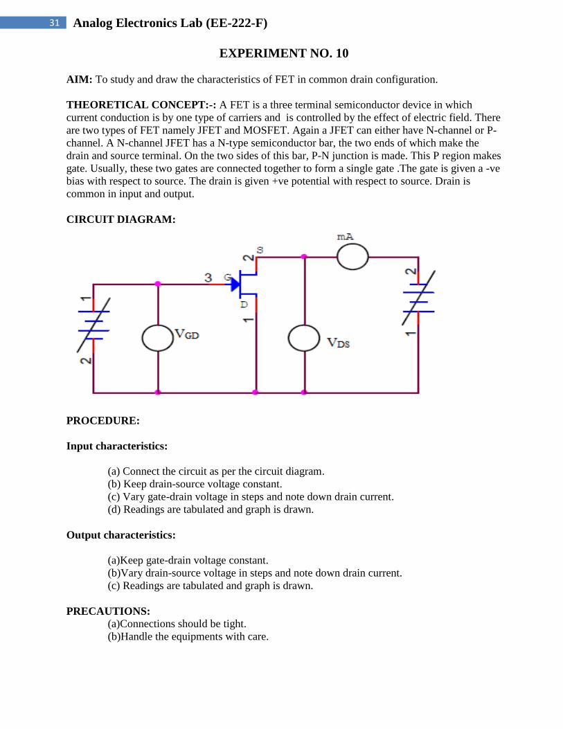
CIRCUIT DIAGRAM:
PROCEDURE:
Input characteristics:
(a) Connect the circuit as per the circuit diagram.
(b) Keep drain-source voltage constant.
(c) Vary gate-drain voltage in steps and note down drain current.
(d) Readings are tabulated and graph is drawn.
Output characteristics:
(a)Keep gate-drain voltage constant.
(b)Vary drain-source voltage in steps and note down drain current.
(c) Readings are tabulated and graph is drawn.
PRECAUTIONS:
(a)Connections should be tight.
(b)Handle the equipments with care.

32 Analog Electronics Lab (EE-222-F)
OBSERVATION TABLE:
GRAPH:
RESULT AND COMMENTS: Input and output characteristics is obtained.