rao pahald singh group of institutions … manual.pdf1 basics of electronics (ece -103 f) basics of...
TRANSCRIPT
1 BASICS OF ELECTRONICS (ECE-103 -F)
Basics of Electronics Lab
(ECE-103-F) LAB MANUAL
I and II SEMESTER
RAO PAHALD SINGH GROUP OF INSTITUTIONS BALANA(MOHINDER GARH)123029
Department Of Electronics and Communication Engg.
RPS CET, Balana (M/Garh)
2 BASICS OF ELECTRONICS (ECE-103 -F)
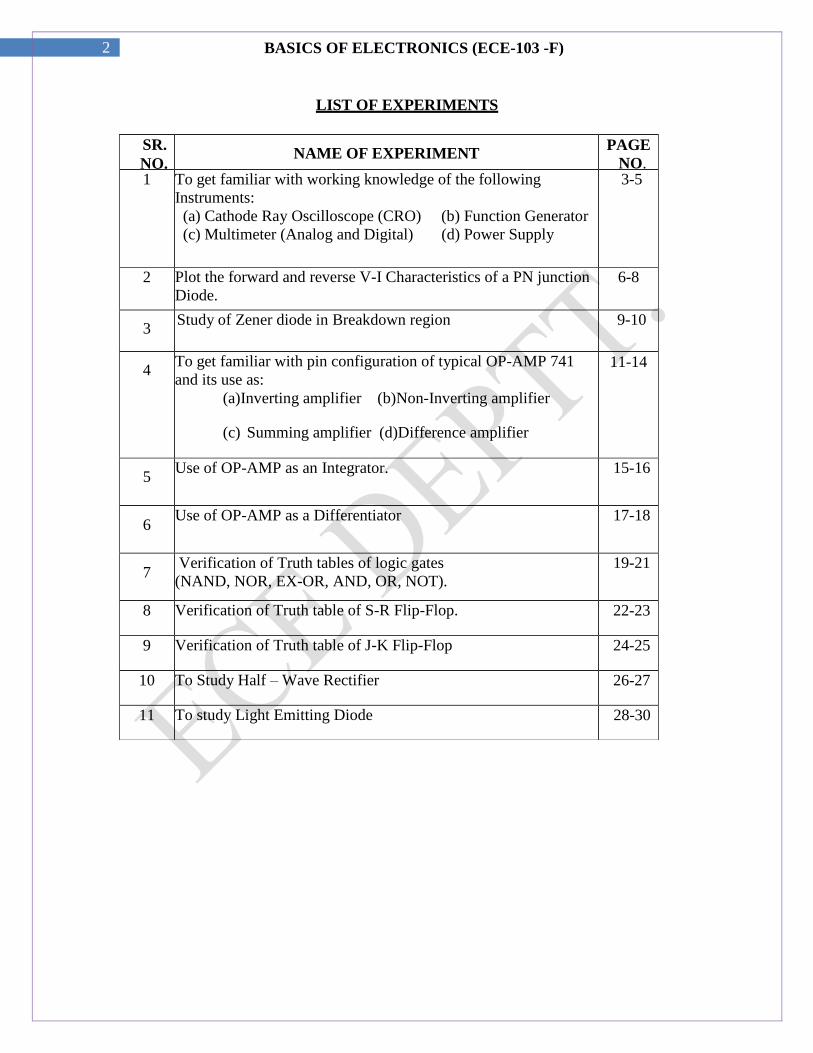
LIST OF EXPERIMENTS
SR.
NO. NAME OF EXPERIMENT
PAGE
NO. 1 To get familiar with working knowledge of the following
Instruments:
(a) Cathode Ray Oscilloscope (CRO) (b) Function Generator
(c) Multimeter (Analog and Digital) (d) Power Supply
Generator
(c) Multimeter (Analog and Digital) (d) Power
Supply
3-5
2 Plot the forward and reverse V-I Characteristics of a PN junction
Diode.
6-8
3 Study of Zener diode in Breakdown region
.
9-10
4 To get familiar with pin configuration of typical OP-AMP 741
and its use as:
(a)Inverting amplifier (b)Non-Inverting amplifier
(c) Summing amplifier (d)Difference amplifier
11-14
5 Use of OP-AMP as an Integrator.
.
15-16
6 Use of OP-AMP as a Differentiator
.
17-18
7 Verification of Truth tables of logic gates
(NAND, NOR, EX-OR, AND, OR, NOT).
19-21
8 Verification of Truth table of S-R Flip-Flop. 22-23
9 Verification of Truth table of J-K Flip-Flop 24-25
10 To Study Half – Wave Rectifier
26-27
11 To study Light Emitting Diode 28-30
3 BASICS OF ELECTRONICS (ECE-103 -F)
EXPERIMENT NO: 1
AIM: To get familiar with working knowledge of the following Instruments:
(a) Cathode Ray Oscilloscope (CRO) (b) Function Generator
(c) Multimeter (Analog and Digital) (d) Power Supply
THEORETICAL CONCEPT:
(a)CATHODE RAY OSCILLOSCOPE
The cathode-ray oscilloscope (CRO) is a common laboratory instrument that provides
accurate time and amplitude measurements of voltage signals over a wide range of
frequencies. Its reliability, stability, and ease of operation make it suitable as a general
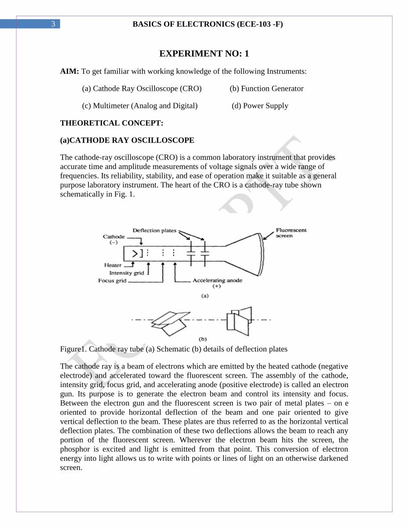
purpose laboratory instrument. The heart of the CRO is a cathode-ray tube shown
schematically in Fig. 1.
Figure1. Cathode ray tube (a) Schematic (b) details of deflection plates
The cathode ray is a beam of electrons which are emitted by the heated cathode (negative
electrode) and accelerated toward the fluorescent screen. The assembly of the cathode,
intensity grid, focus grid, and accelerating anode (positive electrode) is called an electron
gun. Its purpose is to generate the electron beam and control its intensity and focus.
Between the electron gun and the fluorescent screen is two pair of metal plates – on e
oriented to provide horizontal deflection of the beam and one pair oriented to give
vertical deflection to the beam. These plates are thus referred to as the horizontal vertical
deflection plates. The combination of these two deflections allows the beam to reach any
portion of the fluorescent screen. Wherever the electron beam hits the screen, the
phosphor is excited and light is emitted from that point. This conversion of electron
energy into light allows us to write with points or lines of light on an otherwise darkened
screen.

4 BASICS OF ELECTRONICS (ECE-103 -F)
The voltage output of such a generator is that of a saw tooth wave as shown in Fig. 2.
Figure 2.Voltage difference V between horizontal plates as a function of time t
(b) MULTIMETER
A multimeter is used to make various electrical measurements, such as AC and DC
voltage, AC and DC current, and resistance. It is called a multimeter because it combines
the functions of a voltmeter, ammeter, and ohmmeter. Multimeters may also have other
functions, such as diode and continuity tests. The descriptions and pictures that follow are
specific to the Fluke 73 Series III Multimeter, but other multimeters are similar.
(c) FUNCTION GENERATOR
A function generator is a device that can produce various patterns of voltage at a variety
of frequencies and amplitudes.
It is used to test the response of circuits to common input signals. The electrical leads
from the device are attached to the ground and signal input terminals of the device under
test.
Features and controls
Most function generators allow the user to choose the shape of the output from a small
number of options.
-Square wave - The signal goes directly from high to low voltage.
-Sine wave - The signal curves like a sinusoid from high to low voltage.

5 BASICS OF ELECTRONICS (ECE-103 -F)
-Triangle wave - The signal goes from high to low voltage at a fixed rate.
The amplitude control on a function generator varies the voltage difference between the
high and low voltage of the output signal.
The direct current (DC) offset control on a function generator varies the average voltage
of a signal relative to the ground.
The frequency control of a function generator controls the rate at which output signal
oscillates. On some function generators, the frequency control is a combination of
different controls.
One set of controls chooses the broad frequency range (order of magnitude) and the other
selects the precise frequency. This allows the function generator to handle the enormous
variation in frequency scale needed for signals.
(d)POWER SUPPLY
There are many types of power supply. Most are designed to convert high voltage AC
mains electricity to a suitable low voltage supply for electronic circuits and other devices.
A power supply can by broken down into a series of blocks, each of which performs a
particular function.
For example a 5V regulated supply:
Each of the blocks is described in more detail below:
Transformer- steps down high voltage AC mains to low voltage AC.
Rectifier- converts AC to DC, but the DC output is varying.
Smoothing- smoothes the DC from varying greatly to a small ripple.
Regulator- eliminates ripple by setting DC output to a fixed voltage.
6 BASICS OF ELECTRONICS (ECE-103 -F)
EXPERIMENT NO: 2
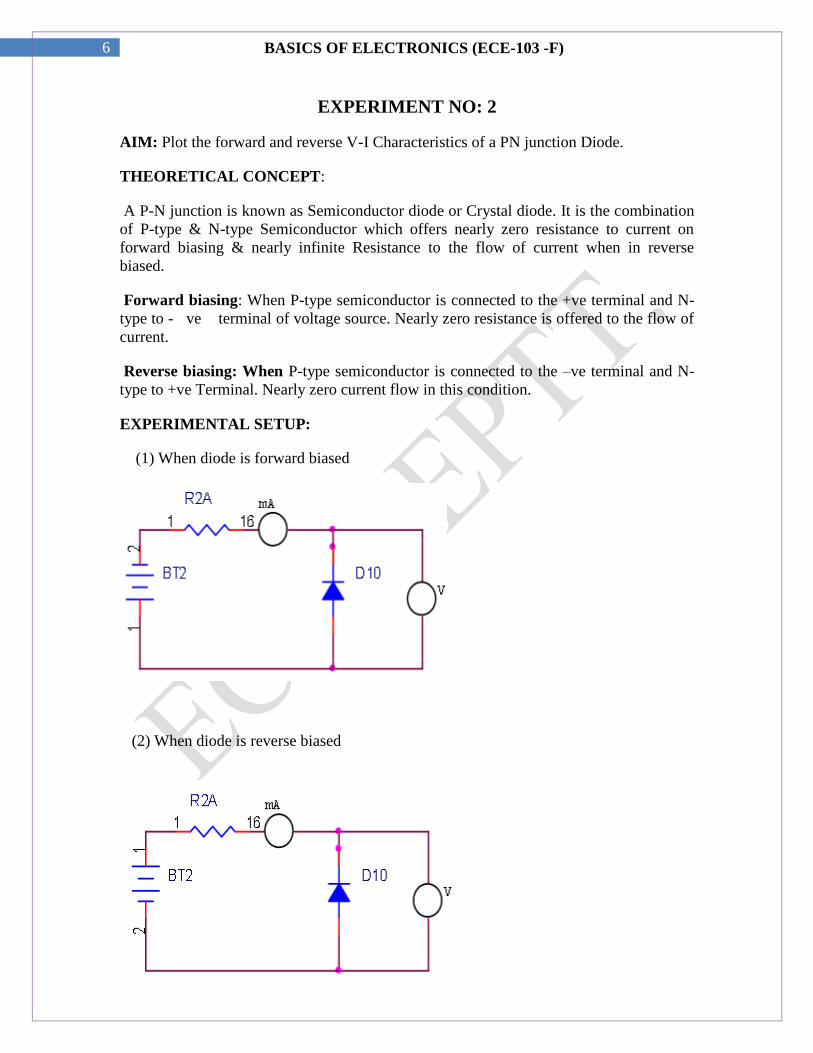
AIM: Plot the forward and reverse V-I Characteristics of a PN junction Diode.
THEORETICAL CONCEPT:
A P-N junction is known as Semiconductor diode or Crystal diode. It is the combination
of P-type & N-type Semiconductor which offers nearly zero resistance to current on
forward biasing & nearly infinite Resistance to the flow of current when in reverse
biased.
Forward biasing: When P-type semiconductor is connected to the +ve terminal and N-
type to - ve terminal of voltage source. Nearly zero resistance is offered to the flow of
current.
Reverse biasing: When P-type semiconductor is connected to the –ve terminal and N-
type to +ve Terminal. Nearly zero current flow in this condition.
EXPERIMENTAL SETUP:
(1) When diode is forward biased
(2) When diode is reverse biased

7 BASICS OF ELECTRONICS (ECE-103 -F)
SPECIFICATION OF APPARATUS USED: Diode Characteristics Kit, Power Supply,
Ammeter (0-20mA), Voltmeter (0-20V), Connecting Leads
PROCEDURE:
1. Connect the circuit as shown in figure.
2. Switch on the power supply.
3. Vary the value of input dc supply in steps.
4. Note down the ammeter & voltmeter readings for each step.
5. Plot the graph of Voltage Vs Current
6. Connect the circuit as shown in figure.
PRECAUTIONS:
1. While doing the experiment do not exceed the ratings of the diode. This may lead
to damage the diode.
2. Connect voltmeter and Ammeter in correct polarities as shown in the circuit
diagram.
3. Do not switch ON the power supply unless you have checked the circuit
connections as per the circuit diagram.
OBSERVATION DATA:
SNo. When diode is forward biased When diode is reverse biased
Current(mA) Voltage(V) Current(µA) Voltage(V)
8 BASICS OF ELECTRONICS (ECE-103 -F)
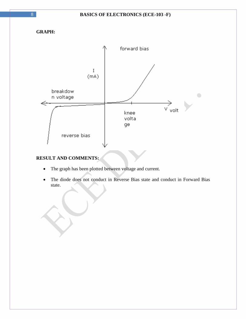
GRAPH:
RESULT AND COMMENTS:
The graph has been plotted between voltage and current.
The diode does not conduct in Reverse Bias state and conduct in Forward Bias
state.
9 BASICS OF ELECTRONICS (ECE-103 -F)
EXPERIMENT NO: 3
AIM: Study of Zener diode in Breakdown region
THEORETICAL CONCEPT: An ideal P-N Junction diode does not conduct in reverse
biased condition. A zener diode conducts excellently even in reverse biased condition.
These diodes operate at a precise value of voltage called break down voltage. A zener
diode when forward biased behaves like an ordinary P-N junction diode. A zener diode
when reverse biased can either undergo avalanche break down or zener break down.
Avalanche breakdown:-If both p-side and n-side of the diode are lightly doped,
depletion region at the junction widens. Application of a very large electric field at the
junction may rupture covalent bonding between electrons. Such rupture leads to the
generation of a large number of charge carriers resulting in avalanche multiplication.
Zener breakdown:-If both p-side and n-side of the diode are heavily doped, depletion
region at the junction reduces. Application of even a small voltage at the junction
ruptures covalent bonding and generates large number of charge carriers. Such sudden
increase in the number of charge carriers results in zener mechanism.
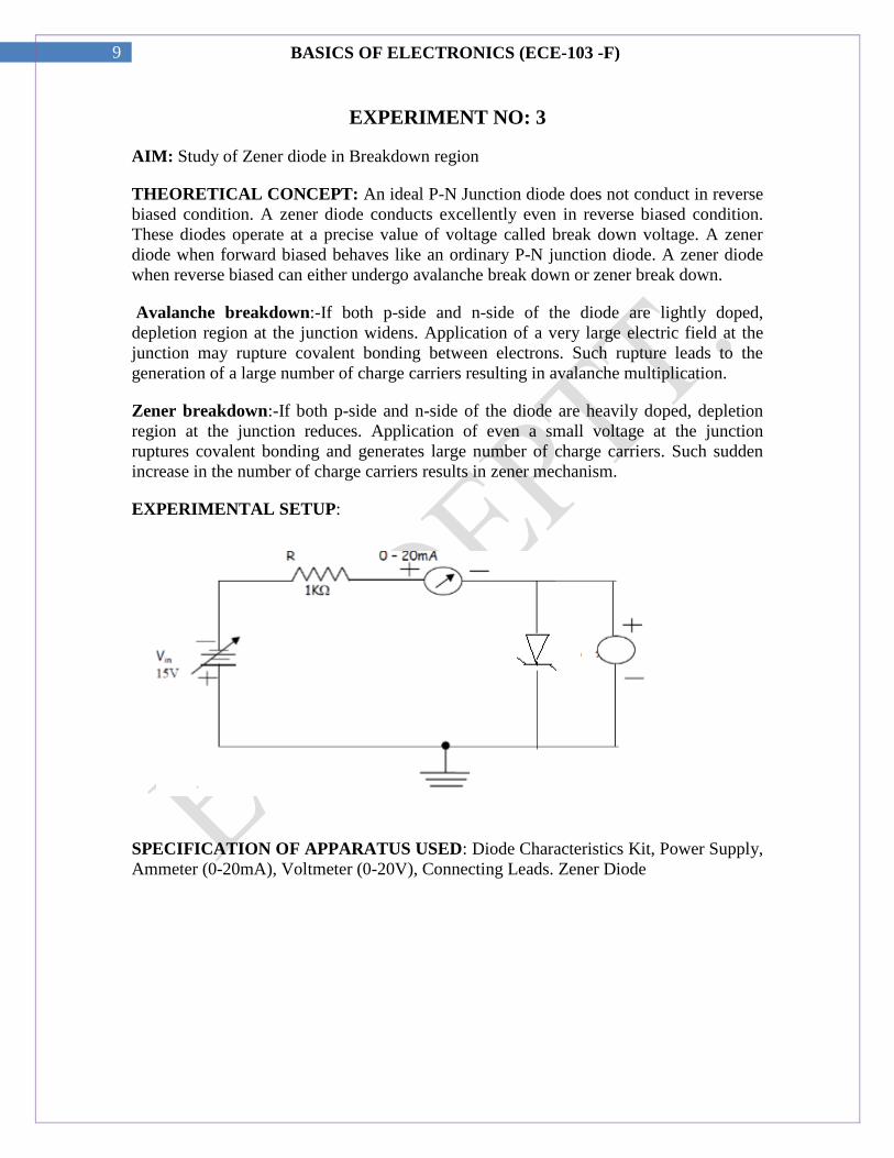
EXPERIMENTAL SETUP:
00-2V
SPECIFICATION OF APPARATUS USED: Diode Characteristics Kit, Power Supply,
Ammeter (0-20mA), Voltmeter (0-20V), Connecting Leads. Zener Diode

10 BASICS OF ELECTRONICS (ECE-103 -F)
PROCEDURE:
1. Connect the circuit as shown in figure.
2. Vary Vz gradually and note down the corresponding readings of Iz.
1. Step Size is not fixed because of non linear curve and vary the X-axis variable
(i.e. if output variation is more, decrease input step size and vice versa).
3. Tabulate different reverse currents obtained for different reverse voltages.
PRECAUTIONS:
1. While doing the experiment do not exceed the ratings of the diode. This may lead
to damage the diode.
2. Connect voltmeter and Ammeter in correct polarities as shown in the circuit
diagram.
4. Do not switch ON the power supply unless you have checked the circuit
connections as per the circuit diagram.
OBSERVATION DATA:
Reverse voltage across diode
Vz(volts)
Reverse current through the diode
Iz(mA)
RESULT AND COMMENTS:
The Zener diode characteristics have been studied.
APPLICATIONS:
1. Voltage regulation
2. Meter protection
3. Zener diode as a peak clipper
4. Zener diode as a reference element
11 BASICS OF ELECTRONICS (ECE-103 -F)
EXPERIMENT NO. 4
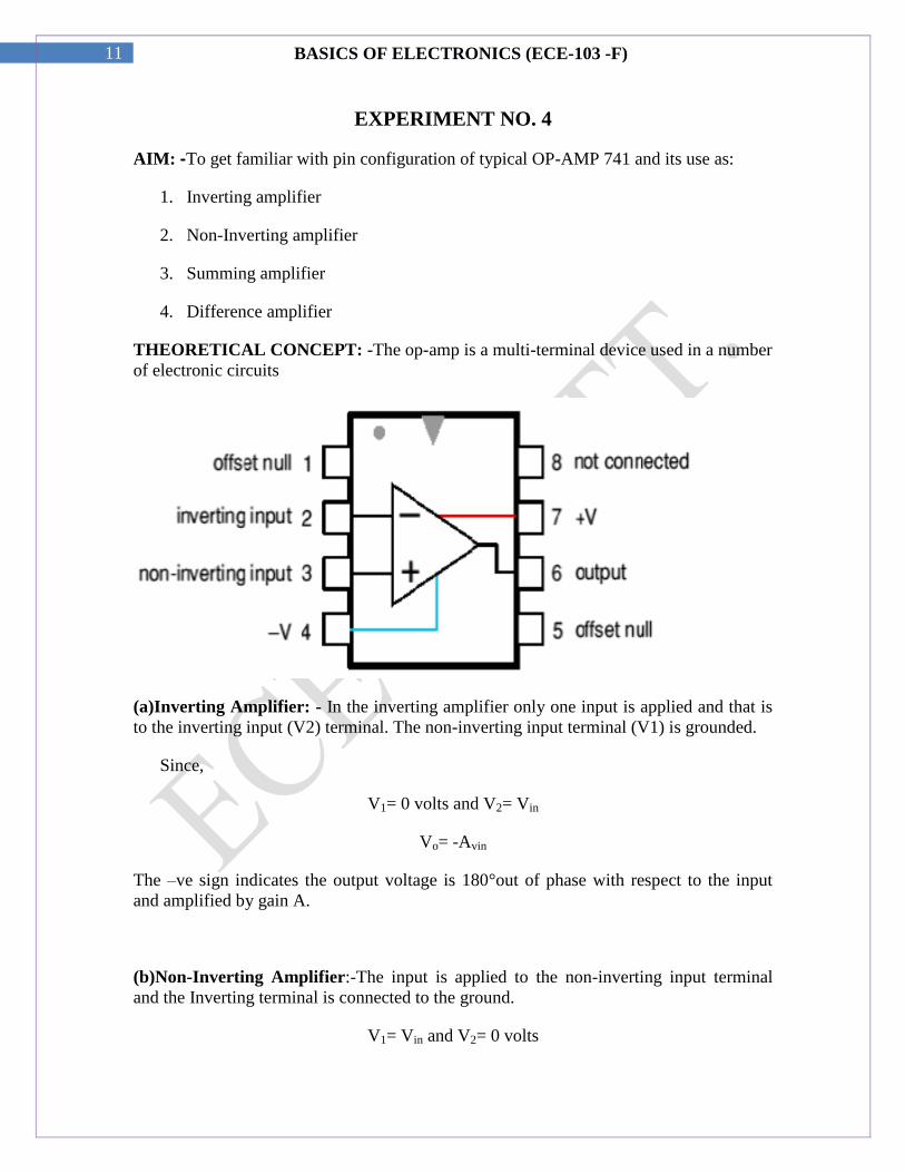
AIM: ‐To get familiar with pin configuration of typical OP-AMP 741 and its use as:
1. Inverting amplifier
2. Non-Inverting amplifier
3. Summing amplifier
4. Difference amplifier
THEORETICAL CONCEPT: -The op-amp is a multi-terminal device used in a number
of electronic circuits
(a)Inverting Amplifier: - In the inverting amplifier only one input is applied and that is
to the inverting input (V2) terminal. The non-inverting input terminal (V1) is grounded.
Since,
V1= 0 volts and V2= Vin
Vo= -Avin
The –ve sign indicates the output voltage is 180°out of phase with respect to the input
and amplified by gain A.
(b)Non-Inverting Amplifier:-The input is applied to the non-inverting input terminal
and the Inverting terminal is connected to the ground.
V1= Vin and V2= 0 volts
12 BASICS OF ELECTRONICS (ECE-103 -F)
Vo= Avin
The output voltage is larger than the input voltage by gain A & is in phase with the input
signal.
(c)Summing Amplifier:
If each input voltage is amplified by a different factor in other words weighted differently
at the output, the circuit is called then summing amplifier.
Vo -
The circuit can be used as averaging circuit, in which output voltage is equal to average
of all the input voltages.
In this case, Ra=Rb=Rc=R and Rf/R=1/n, where n is number of inputs.
Here Rf/R=1/3
Vo=-(Va+Vb+Vc)/3
In all these applications input could be either ac or dc.
c) Difference Amplifier:
The output voltage is directly proportional to the input difference of two voltages:
Vo = (Vin1- Vin2)

13 BASICS OF ELECTRONICS (ECE-103 -F)
EXPERIMENTAL SETUP:
(a)Inverting amplifier b) Noninverting amplifier
(c)Summing Amplifier (d) Difference Amplifier
SPECIFICATION OF APPARATUS USED: - CRO, Function Generator, Bread
Board, 741 IC, ±12V supply, Resistors1KΩ, 10KΩ, and Connecting leads.
PROCEDURE: -
1. Connect the circuit for Inverting, Non-inverting and Summing and Difference
amplifier on a Breadboard.
2. Connect the input terminal of the op-amp to function generator and output
terminal to CRO.
3. Feed input from function generator and observe the output on CRO.
4. Draw the input and output waveforms on graph paper.
14 BASICS OF ELECTRONICS (ECE-103 -F)
PRECAUTIONS:-
1. Do not use open ended wires for connecting to 230 V power supply.
1. Before connecting the power supply plug into socket, ensure power supply should
switched off
2. Ensure all connections should be tight before switching on the power supply.
RESULT AND COMMENTS: -
Desired and Amplified output waveforms are obtained.

15 BASICS OF ELECTRONICS (ECE-103 -F)
EXPERIMENT NO: 5
AIM: Use of OP-AMP as an Integrator.
THEORETICAL CONCEPT:
A circuit in output voltage waveform is an integral of the input voltage waveform is
called an integrator. In this circuit, the feedback resistor of an OP-AMP is replaced by a
capacitor. The output obtained will be an integral of the input wave.
I (t) = v (t) /R
Output Voltage= 1/C v (t)/R dt = -1/RC V (t) dt
The circuit therefore provides an output voltage proportional to the integral of the input
voltage. If the input voltage is a constant, v=V, then the output will be a ramp,
Vo (t) =-1/RC
EXPERIMENTAL SETUP:
Here, the feedback element is a capacitor. The current drawn by OPAMP is zero also the
V2 is virtually grounded.
Therefore i1=if and v2=v1=0
SPECIFICATION OF APPARATUS USED: - CRO, Function Generator, Power
supply, connecting, leads, Integrator circuit kit.
16 BASICS OF ELECTRONICS (ECE-103 -F)
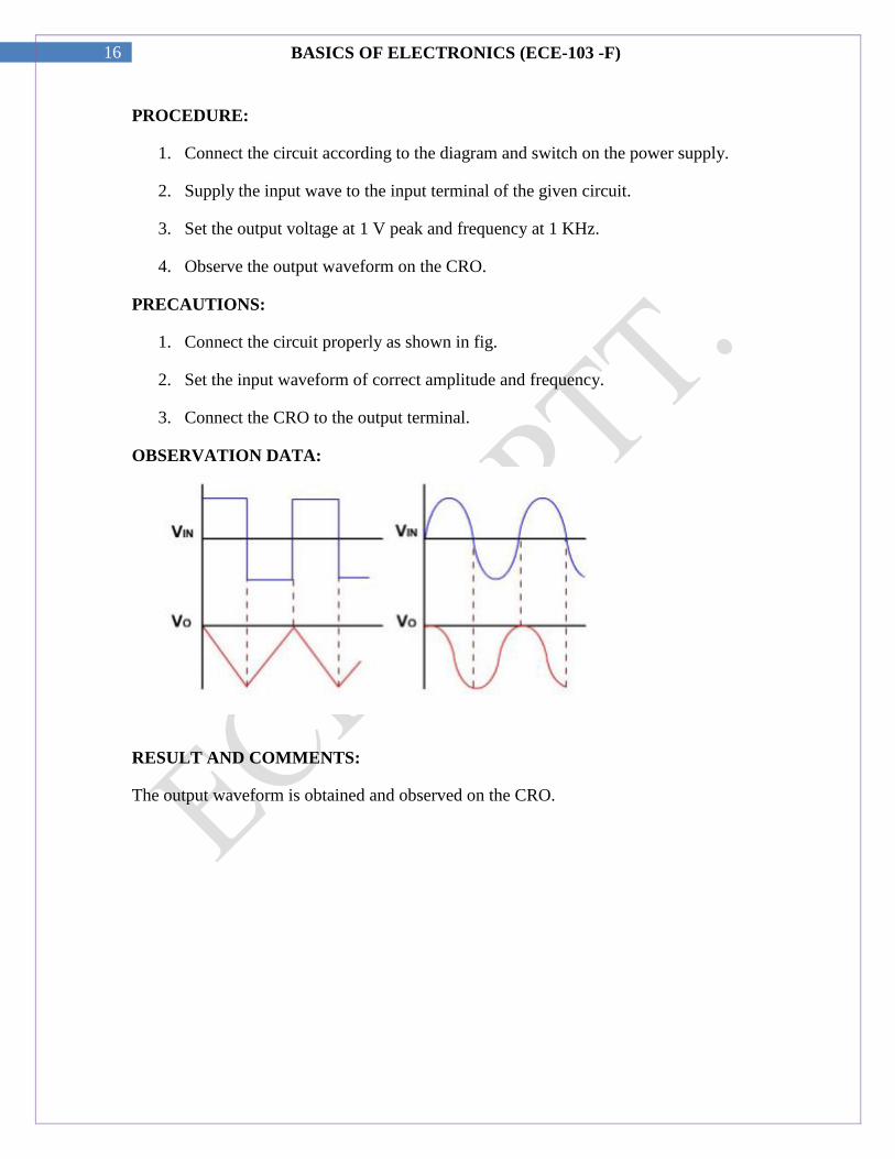
PROCEDURE:
1. Connect the circuit according to the diagram and switch on the power supply.
2. Supply the input wave to the input terminal of the given circuit.
3. Set the output voltage at 1 V peak and frequency at 1 KHz.
4. Observe the output waveform on the CRO.
PRECAUTIONS:
1. Connect the circuit properly as shown in fig.
2. Set the input waveform of correct amplitude and frequency.
3. Connect the CRO to the output terminal.
OBSERVATION DATA:
RESULT AND COMMENTS:
The output waveform is obtained and observed on the CRO.
17 BASICS OF ELECTRONICS (ECE-103 -F)
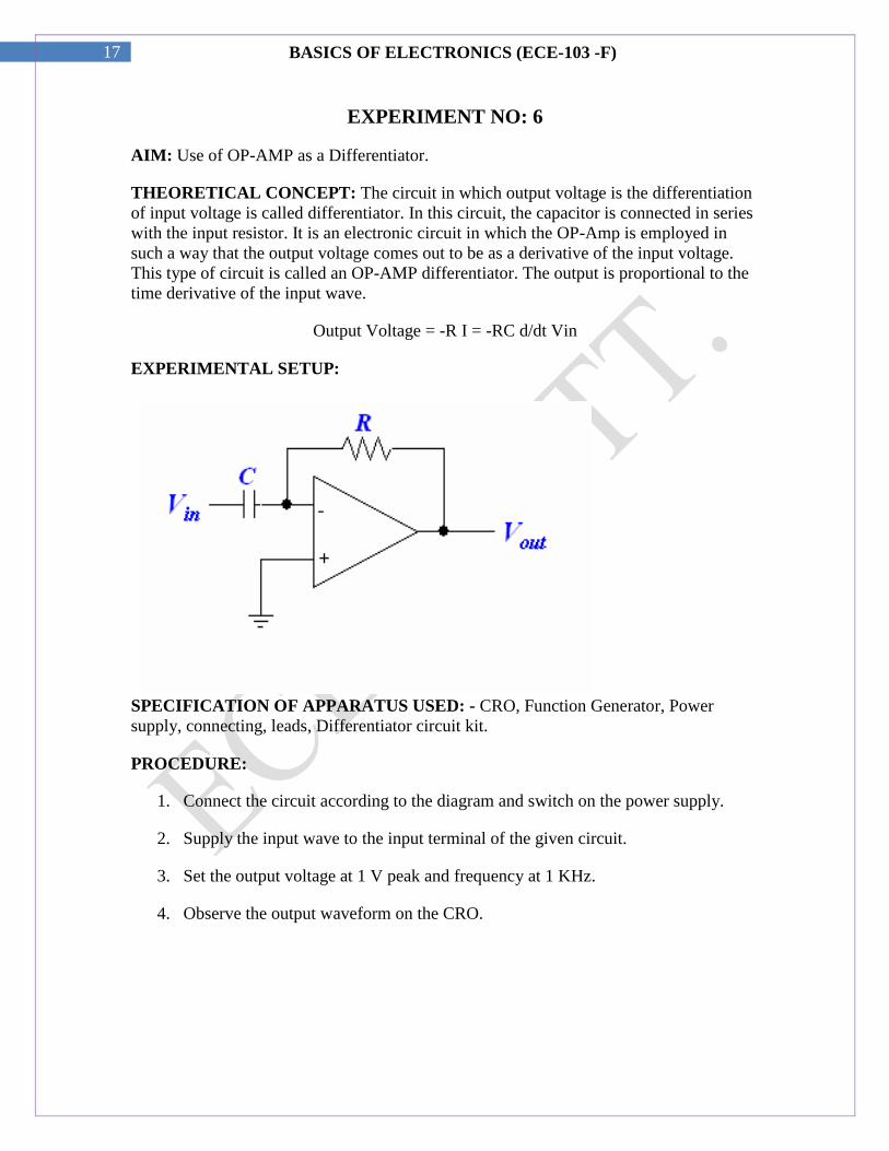
EXPERIMENT NO: 6
AIM: Use of OP-AMP as a Differentiator.
THEORETICAL CONCEPT: The circuit in which output voltage is the differentiation
of input voltage is called differentiator. In this circuit, the capacitor is connected in series
with the input resistor. It is an electronic circuit in which the OP-Amp is employed in
such a way that the output voltage comes out to be as a derivative of the input voltage.
This type of circuit is called an OP-AMP differentiator. The output is proportional to the
time derivative of the input wave.
Output Voltage = -R I = -RC d/dt Vin
EXPERIMENTAL SETUP:
SPECIFICATION OF APPARATUS USED: - CRO, Function Generator, Power
supply, connecting, leads, Differentiator circuit kit.
PROCEDURE:
1. Connect the circuit according to the diagram and switch on the power supply.
2. Supply the input wave to the input terminal of the given circuit.
3. Set the output voltage at 1 V peak and frequency at 1 KHz.
4. Observe the output waveform on the CRO.
18 BASICS OF ELECTRONICS (ECE-103 -F)
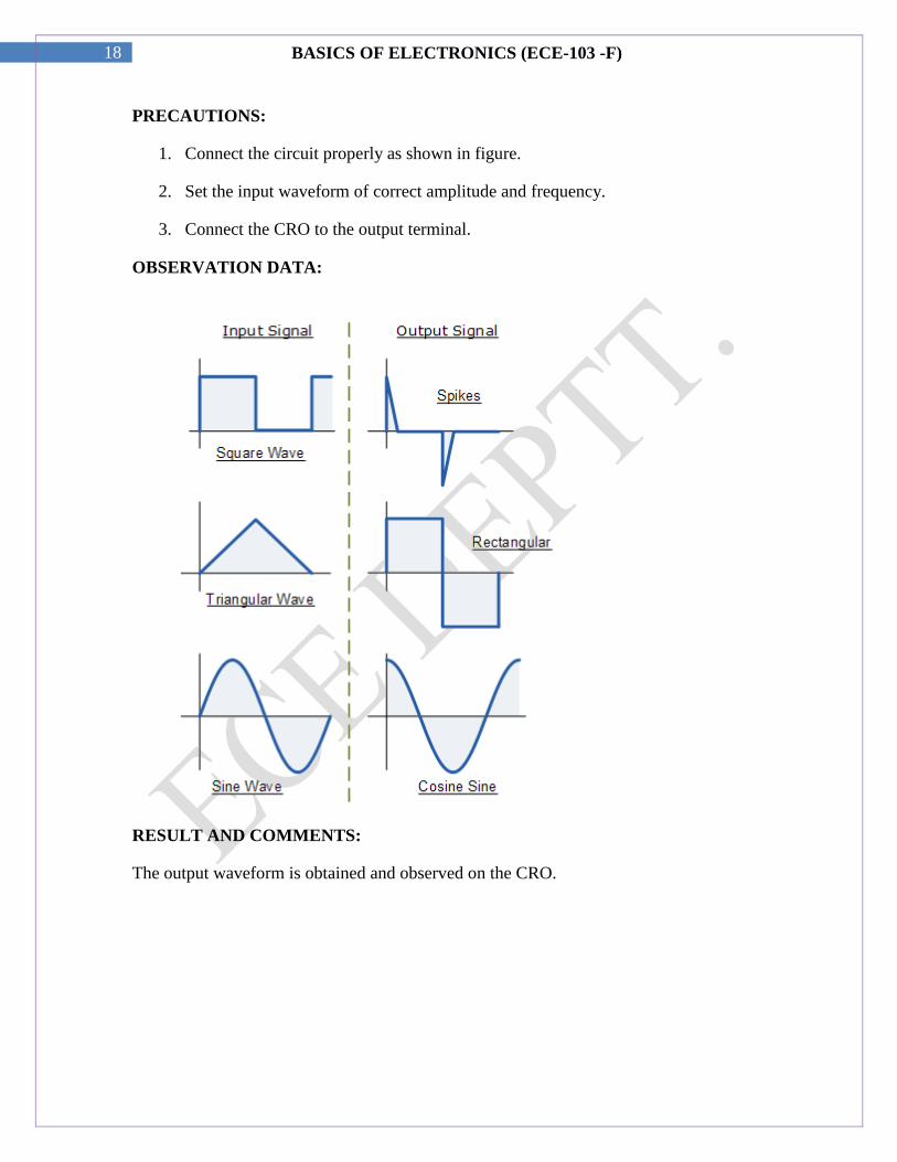
PRECAUTIONS:
1. Connect the circuit properly as shown in figure.
2. Set the input waveform of correct amplitude and frequency.
3. Connect the CRO to the output terminal.
OBSERVATION DATA:
RESULT AND COMMENTS:
The output waveform is obtained and observed on the CRO.
19 BASICS OF ELECTRONICS (ECE-103 -F)
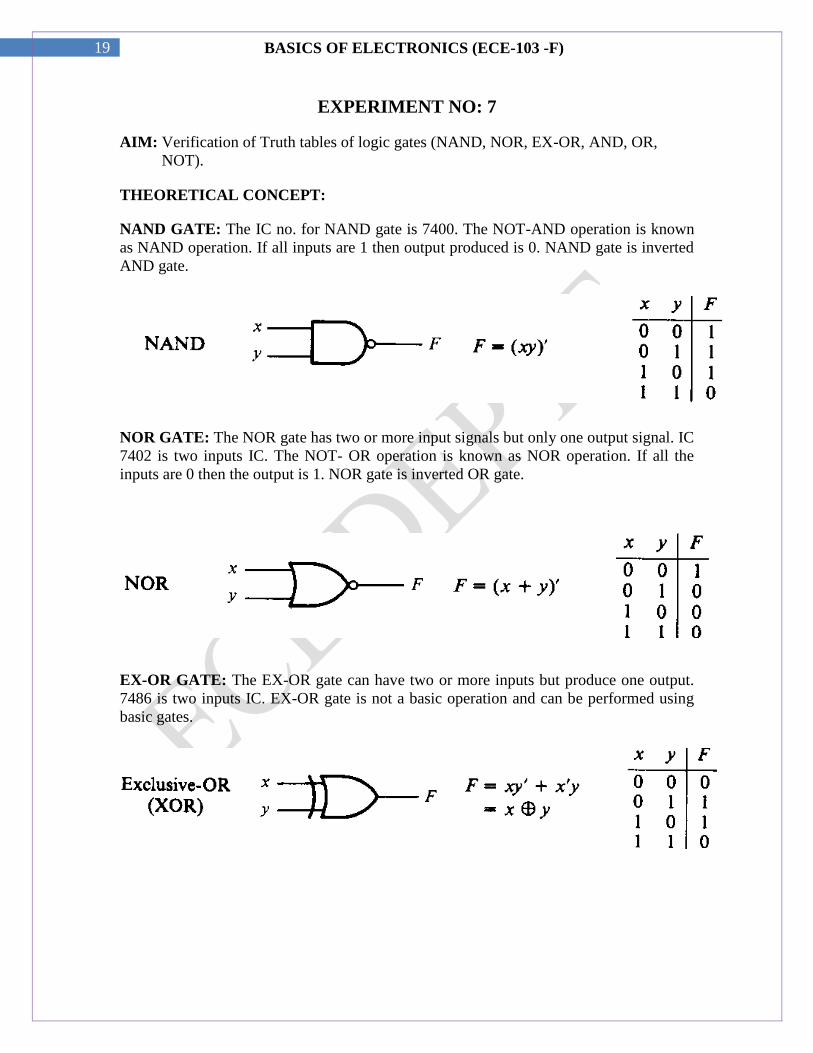
EXPERIMENT NO: 7
AIM: Verification of Truth tables of logic gates (NAND, NOR, EX-OR, AND, OR,
NOT).
THEORETICAL CONCEPT:
NAND GATE: The IC no. for NAND gate is 7400. The NOT-AND operation is known
as NAND operation. If all inputs are 1 then output produced is 0. NAND gate is inverted
AND gate.
NOR GATE: The NOR gate has two or more input signals but only one output signal. IC
7402 is two inputs IC. The NOT- OR operation is known as NOR operation. If all the
inputs are 0 then the output is 1. NOR gate is inverted OR gate.
EX-OR GATE: The EX-OR gate can have two or more inputs but produce one output.
7486 is two inputs IC. EX-OR gate is not a basic operation and can be performed using
basic gates.
20 BASICS OF ELECTRONICS (ECE-103 -F)
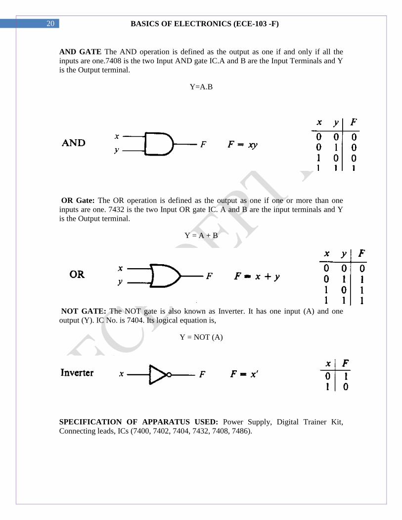
AND GATE The AND operation is defined as the output as one if and only if all the
inputs are one.7408 is the two Input AND gate IC.A and B are the Input Terminals and Y
is the Output terminal.
Y=A.B
OR Gate: The OR operation is defined as the output as one if one or more than one
inputs are one. 7432 is the two Input OR gate IC. A and B are the input terminals and Y
is the Output terminal.
Y = A + B
NOT GATE: The NOT gate is also known as Inverter. It has one input (A) and one
output (Y). IC No. is 7404. Its logical equation is,
Y = NOT (A)
SPECIFICATION OF APPARATUS USED: Power Supply, Digital Trainer Kit,
Connecting leads, ICs (7400, 7402, 7404, 7432, 7408, 7486).

21 BASICS OF ELECTRONICS (ECE-103 -F)
PROCEDURE:
1. Fix the IC’s on breadboard and give the input supply.
2. Connect the +ve terminal of supply to pin 14 and -ve to pin 7.
3. Give input at pin 1, 2 and take output from pin 3. It is same for all except NOT
and NOR IC.
4. For NOR, pin 1 is output and pin 2 and3 are inputs.
5. For NOT, pin 1 is input and pin 2 is output.
6. Note the values of output for different combination of inputs and draw the
TRUTH TABLE.
PRECAUTIONS:
1. Make the connections according to the IC pin diagram.
2. The connections should be tight.
3. The Vcc and ground should be applied carefully at the specified pin only.
OBSERVATION DATA:
AND
OR NOR NAND EX-OR
Inputs Output Inputs Output Inputs Output Inputs Output Inputs Output
RESULT AND COMMENTS: We have learnt all the gates ICs according to the IC pin
diagram.
22 BASICS OF ELECTRONICS (ECE-103 -F)
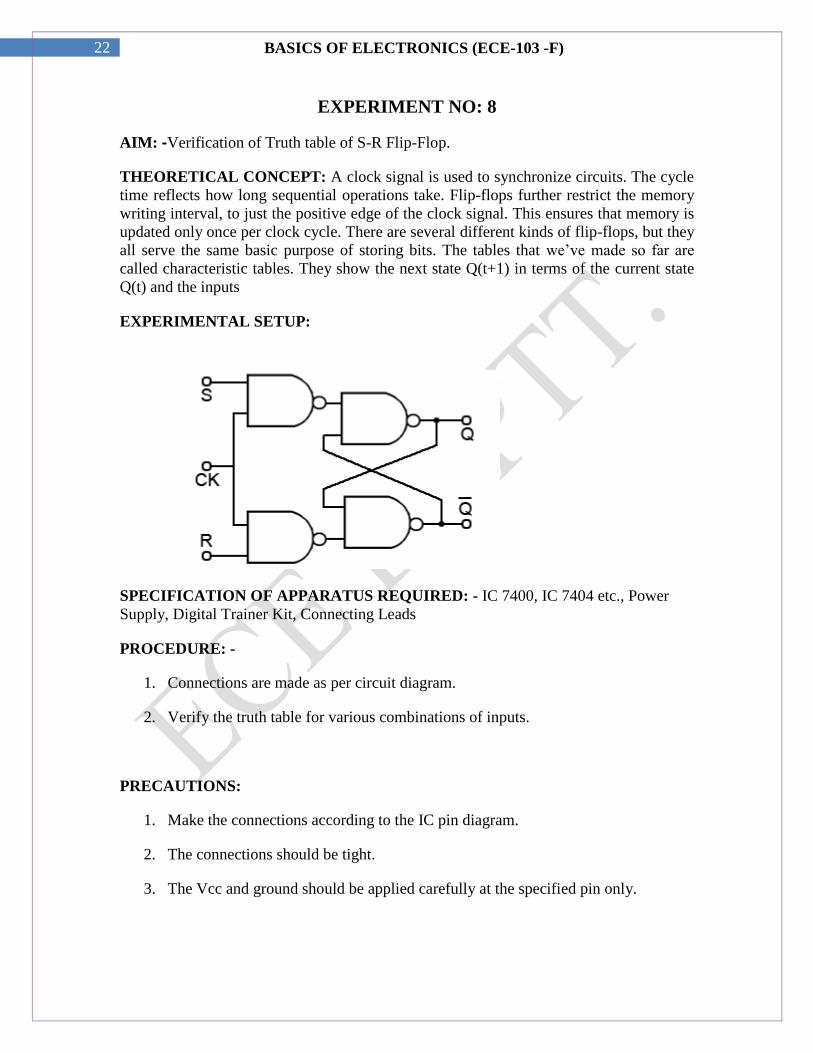
EXPERIMENT NO: 8
AIM: ‐Verification of Truth table of S-R Flip-Flop.
THEORETICAL CONCEPT: A clock signal is used to synchronize circuits. The cycle
time reflects how long sequential operations take. Flip-flops further restrict the memory
writing interval, to just the positive edge of the clock signal. This ensures that memory is
updated only once per clock cycle. There are several different kinds of flip-flops, but they
all serve the same basic purpose of storing bits. The tables that we’ve made so far are
called characteristic tables. They show the next state Q(t+1) in terms of the current state
Q(t) and the inputs
EXPERIMENTAL SETUP:
SPECIFICATION OF APPARATUS REQUIRED: - IC 7400, IC 7404 etc., Power
Supply, Digital Trainer Kit, Connecting Leads
PROCEDURE: -
1. Connections are made as per circuit diagram.
2. Verify the truth table for various combinations of inputs.
PRECAUTIONS:
1. Make the connections according to the IC pin diagram.
2. The connections should be tight.
3. The Vcc and ground should be applied carefully at the specified pin only.

23 BASICS OF ELECTRONICS (ECE-103 -F)
OBSERVATION DATA:
S R Qn Qn+1 Condition
0 0 NC NC No Change
1 0 1 0 Set
0 1 0 1 Reset
1 1 0 0 Invalid
RESULT AND COMMENTS: We have learnt S-R Flip-flop according to their circuit
diagram and working operation.
24 BASICS OF ELECTRONICS (ECE-103 -F)
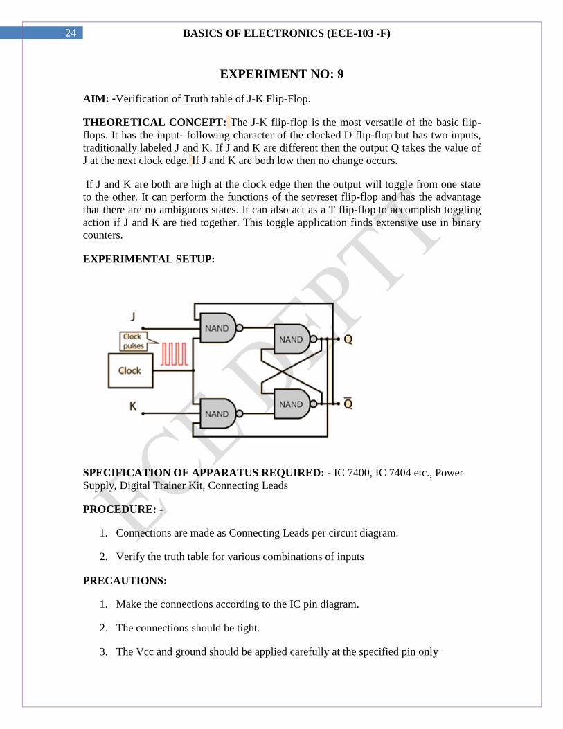
EXPERIMENT NO: 9
AIM: ‐Verification of Truth table of J-K Flip-Flop.
THEORETICAL CONCEPT: The J-K flip-flop is the most versatile of the basic flip-
flops. It has the input- following character of the clocked D flip-flop but has two inputs,
traditionally labeled J and K. If J and K are different then the output Q takes the value of
J at the next clock edge. If J and K are both low then no change occurs.
If J and K are both are high at the clock edge then the output will toggle from one state
to the other. It can perform the functions of the set/reset flip-flop and has the advantage
that there are no ambiguous states. It can also act as a T flip-flop to accomplish toggling
action if J and K are tied together. This toggle application finds extensive use in binary
counters.
EXPERIMENTAL SETUP:
SPECIFICATION OF APPARATUS REQUIRED: - IC 7400, IC 7404 etc., Power
Supply, Digital Trainer Kit, Connecting Leads
PROCEDURE: -
1. Connections are made as Connecting Leads per circuit diagram.
2. Verify the truth table for various combinations of inputs
PRECAUTIONS:
1. Make the connections according to the IC pin diagram.
2. The connections should be tight.
3. The Vcc and ground should be applied carefully at the specified pin only

25 BASICS OF ELECTRONICS (ECE-103 -F)
OBSERVATION DATA:
RESULT AND COMMENTS: We have learnt S-R Flip-flop according to their circuit
diagram and working operation.
Inputs Output Comments
J K Clock Q Q’
0 0 Q Q’ No Change
0 1 0 1 Reset
1 0 1 0 Set
1 1 Q
’
Q Toggle
26 BASICS OF ELECTRONICS (ECE-103 -F)
EXPERIMENT NO.10
AIM: To study half wave rectifier
THEORETICAL CONCEPT: Rectification is a process of conversion of AC to DC. In
half-wave rectifier, only one diode is used. During +ve half Cycle the diode is forward
biased &, it conducts current through the load resistor R .During –ve half cycle diode is
reverse biased Hence, no current flow through the circuit. Only +ve half cycle appears
across the load, whereas, the –ve half Cycle is suppressed.
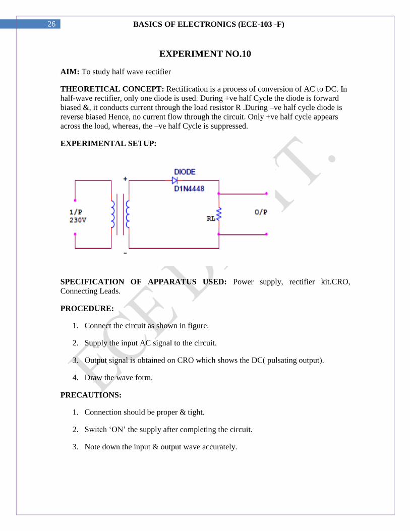
EXPERIMENTAL SETUP:
SPECIFICATION OF APPARATUS USED: Power supply, rectifier kit.CRO,
Connecting Leads.
PROCEDURE:
1. Connect the circuit as shown in figure.
2. Supply the input AC signal to the circuit.
3. Output signal is obtained on CRO which shows the DC( pulsating output).
4. Draw the wave form.
PRECAUTIONS:
1. Connection should be proper & tight.
2. Switch ‘ON’ the supply after completing the circuit.
3. Note down the input & output wave accurately.
27 BASICS OF ELECTRONICS (ECE-103 -F)
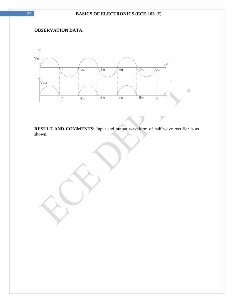
OBSERVATION DATA:
Waveform:
RESULT AND COMMENTS: Input and output waveform of half wave rectifier is as
shown.

28 BASICS OF ELECTRONICS (ECE-103 -F)
EXPERIMENT NO. 11
AIM: To study Light emitting diode
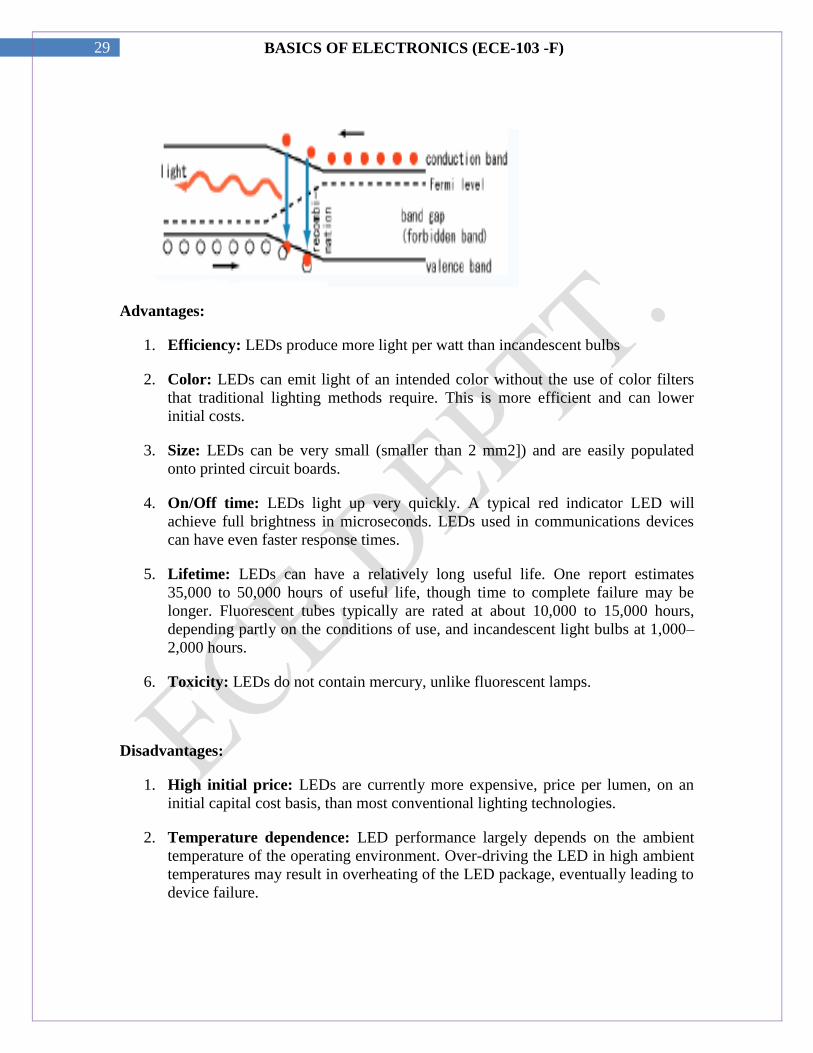
THEORETICAL CONCEPT: The LED consists of a chip of semiconducting material
impregnated, or doped, with impurities to create a p-n junction. As in other diodes,
current flows easily from the p-side, or anode, to the nside or cathode, but not in the
reverse direction. Charge-carriers—electrons and holes—flow into the junction from
electrodes with different voltages. When an electron meets a hole, it falls into a lower
energy level, and releases energy in the form of a photon.
The wavelength of the light emitted, and therefore its color, depends on the band gap
energy of the materials forming the p-n junction. In silicon or germanium diodes, the
electrons and holes recombine by a non-radiative transition which produces no optical
emission, because these are indirect band gap materials. The materials used for the LED
have a direct band gap with energies corresponding to near-infrared, visible or near-
ultraviolet light.
LED development began with infrared and red devices made with gallium arsenide.
Advances in materials science have made possible the production of devices with ever-
shorter wavelengths, producing light in a variety of colors.
LEDs are usually built on an n-type substrate, with an electrode attached to the p-type
layer deposited on its surface. P-type substrates, while less common, occur as well. Many
commercial LEDs, especially GaN/InGaN, also use sapphire substrate.
Most materials used for LED production have very high refractive indices. This means
that much light will be reflected back in to the material at the material/air surface
interface. Therefore Light extraction in LEDs is an important aspect of LED production,
subject to much research and development.
EXPERIMENTAL SETUP
29 BASICS OF ELECTRONICS (ECE-103 -F)
Advantages:
1. Efficiency: LEDs produce more light per watt than incandescent bulbs
2. Color: LEDs can emit light of an intended color without the use of color filters
that traditional lighting methods require. This is more efficient and can lower
initial costs.
3. Size: LEDs can be very small (smaller than 2 mm2]) and are easily populated
onto printed circuit boards.
4. On/Off time: LEDs light up very quickly. A typical red indicator LED will
achieve full brightness in microseconds. LEDs used in communications devices
can have even faster response times.
5. Lifetime: LEDs can have a relatively long useful life. One report estimates
35,000 to 50,000 hours of useful life, though time to complete failure may be
longer. Fluorescent tubes typically are rated at about 10,000 to 15,000 hours,
depending partly on the conditions of use, and incandescent light bulbs at 1,000–
2,000 hours.
6. Toxicity: LEDs do not contain mercury, unlike fluorescent lamps.
Disadvantages:
1. High initial price: LEDs are currently more expensive, price per lumen, on an
initial capital cost basis, than most conventional lighting technologies.
2. Temperature dependence: LED performance largely depends on the ambient
temperature of the operating environment. Over-driving the LED in high ambient
temperatures may result in overheating of the LED package, eventually leading to
device failure.

30 BASICS OF ELECTRONICS (ECE-103 -F)
3. Voltage sensitivity: LEDs must be supplied with the voltage above the threshold
and a current below the rating. This can involve series resistors or current-
regulated power supplies.