r em microelectronic - marin sa v6118 © 2008, em microelectronic-marin sa 06/08 – rev.m ... pad...
TRANSCRIPT

R
V6118
Copyright © 2008, EM Microelectronic-Marin SA 06/08 – rev.M
1 www.emmicroelectronic.com
2, 4 and 8 Mutiplex LCD Driver Description The V6118 is a universal low multiplex LCD driver. The version V6118 2 drives two ways multiplex (two blackplanes) LCD, the version V6118 4, four way multiplex LCD , and the V6118 8, eight way multiplex LCD. The display refresh is handled on chip via a 40 x 8 bit RAM which holds the LCD content driven by the driver. LCD pixels (or segments) are addressed on a one to one basis with the 40 x 8 bit RAM (a set bit corresponds to an activated LCD pixel). The V6118 has very low dynamic current consumption , 150 µA max., making it particularly attractive for portable and battery powered applications. The wide operating range on both the logic (VDD) and the LCD (VLCD) supply voltages offers much application flexibility. The LCD bias generation is internal. The voltage bias levels can also be provided externally for applications having large pixels sizes. The V6118 can be used as a column only driver for cascading in large display applications. In the column only mode, 40 column outputs are available to address the display. A BLANK function is provided to blank the LCD, useful at power up to hold the display blank until the microprocessor has updated the display RAM. Applications □ Balances and scales □ Automotive displays □ Utility meters □ Large displays (public information panel etc.) □ Pagers □ Portable, battery operated products □ Telephones
Features □ V6118 2 is 2 way multiplex with 2 rows and 38 columns □ V6118 4 is 4 way multiplex with 4 rows and 36 columns □ V6118 8 is 8 way multiplex with 8 rows and 32 columns □ Low dynamic current, 150 µA max. □ Low standby current, 1 µA max. at +25°C □ Voltage bias and mux signal generation on chip □ Display refresh on chip, 40 x 8 RAM for display storage □ Display RAM addressable as 8, 40 bits words □ Column driver only mode to have 40 column outputs □ Crossfree cascadable for large LCD applications □ Separate logic and LCD supply voltage pins □ Wide power supply range: VDD: 2 to 6V, VLCD: 2 to 8V □ BLANK function for LCD blanking on power up etc. □ Voltage bias inputs for applications with large pixel
sizes □ Bit mapped □ Serial input / output □ Very low external component count □ -40 to + 85 °C temperature range □ No busy states □ LCD updating synchronized to the LCD refresh signal □ QFP52 and TAB packages
Typical Operating Configuration
Fig. 1
Pad Assignment
Fig. 2
EM MICROELECTRONIC - MARIN SA

R
V6118
Copyright © 2008, EM Microelectronic-Marin SA 06/08 – rev.M
2 www.emmicroelectronic.com
Absolute Maximum Ratings
Parameter Symbol Conditions Supply voltage range VDD -0.3V to + 8V LCD supply voltage range VLCD -0.3V to + 9V Voltage at DI, DO, CLK, STR, FR, COL
VLOGIC -0.3V to VDD+0.3V
Voltage at V1 to V3, S1 to S40 VDISP -0.3V to VLCD + 0.3V
Storage temperature range TSTO -65 to +150°C Power dissipation PMAX 100mW Electrostatic discharge max. to MIL-STD-883C method 3015.7 with ref. to VSS
VSMAX 1000V
Maximum soldering conditions TS 250°C x 10s
Table 1 Stresses above these listed maximum ratings may cause permanent damages to the device. Exposure beyond specified operating conditions may affect device reliability or cause malfunction.
Handling Procedures This device has built-in protection against high static voltages or electric fields; however, anti-static precautions must be taken as for any other CMOS component. Unless otherwise specified, proper operation can only occur when all terminal voltages are kept within the voltage range. Unused inputs must always be tied to a defined logic voltage level. Operating Conditions
Parameter Symbol Min Typ Max UnitOperating Temperature
TA -40 +85 °C
Logic supply voltage VDD 2 5 6 V LCD supply voltage VLCD 2 5 8 V
Table 2
Electrical Characteristics VDD = 5V ±10%, VLCD = 2 to 7V and TA = -40 to +85°C, unless otherwise specified
Parameter Symbol Test Conditions Min. Typ. Max. Units Dynamic supply current ILCD See note 1 100 170 μA Dynamic supply current IDD See note 1 at TA = 25°C 0.1 1 μA Dynamic supply current IDD See note 1 3 12 μA Dynamic supply current IDD See note 2 200 280 μA Standby supply current ISS See note 3 at TA = 25°C 0.1 1 μA Control Signals DI, CLK, STR, FR and COL
Input leakage IIN 0 < VIN < VDD 1 100 nA Input capacitance CIN at TA = 25°C 8 pF Low level input voltage VIL 0 0.8 V High level input voltage for DI, STR, FR and COL
VIH 2.0 VDD V
High level input voltage for CLK VIH 3.0 VDD V Data Output DO High level output voltage VOH IH = 4 mA 2.4 V Low level output voltage VOL IL = 4 mA 0.4 V Driver Outputs S1 … S40 Driver impedance (note 4) ROUT IOUT = 10µA, VLCD = 7V 0.5 1.5 kΩ Driver impedance (note 4) ROUT IOUT = 10µA, VLCD = 3V 1.2 2.5 kΩ Driver impedance (note 4) ROUT IOUT = 10µA, VLCD = 2V 9 kΩ Bias impedance V1, V2, V3 (note 5) RBIAS IOUT = 10µA, VLCD = 7V 16 20 kΩ Bias impedance V1, V2, V3 (note 5) RBIAS IOUT = 10µA, VLCD = 3V 18 25 kΩ Bias impedance V1, V2, V3 (note 5) RBIAS IOUT = 10µA, VLCD = 2V 30 kΩ DC output component ± VDC see Tables 4a & 4b,
VLCD = 5V
30
50
mV Table 3
Note 1: All outputs open, STR at VSS, FR = 400 Hz, all other inputs at VDD. Note 2: All outputs open, STR at VSS, FR = 400 Hz, fCLK = 1 MHz, all other inputs at VDD. Note 3: All outputs open, all other inputs at VDD. Note 4: This is the impedance between of the voltage bias level pins (V1, V2 or V3) and the output pins S1 to S40
when a given voltage bias level is driving the outputs (S1 to S40) Note 5: This is the impedance seen at the segment pin. Outputs measured one at a time.
R
V6118
Copyright © 2008, EM Microelectronic-Marin SA 06/08 – rev.M
3 www.emmicroelectronic.com
Column Drivers Outputs FR Polarity COL Column Data Measured* Guaranteed
S1 to S40 logic 1 logic 0 logic 1 ⏐ Sx* - VSS ⏐ S1 to S40 logic 0 logic 0 logic 1 ⏐ VLCD - Sx* ⏐ ¦ VLCD - Sx* ¦ = ¦ Sx* - VSS¦ ± 25 mV S1 to S40 logic 1 logic 0 logic 0 ⏐ VLCD - Sx* ⏐ S1 to S40 logic 0 logic 0 logic 0 ⏐ Sx* - VSS ⏐ ¦ VLCD - Sx* ¦ = ¦ Sx* - VSS¦ ± 25 mV
Table 4a *Sx = the output number (ie. S1 to S40) Row Drivers
Outputs FR Polarity COL Column Data Measured* Guaranteed S1 to Sn* logic 1 logic 1 logic 1 ⏐ VLCD - Sx ⏐ S1 to Sn* logic 0 logic 1 logic 1 ⏐ Sx - VSS ⏐ ¦ VLCD - Sx ¦ = ¦ Sx - VSS¦ ± 25 mV S1 to Sn* logic 1 logic 1 logic 0 ⏐ Sx - VSS ⏐ S1 to Sn* logic 0 logic 1 logic 0 ⏐ VLCD - Sx ⏐ ¦ VLCD - Sx ¦ = ¦ Sx - VSS¦ ± 25 mV
Table 4b *n = the V6118 version no. (ie. 2, 4 or 8) Timing Characteristics VDD = 5V ± 10%, VLCD = 2 to 8V and TA = -40 to +85°C
Parameter Symbol Test Conditions Min. Typ. Max. Units Clock high pulse width tCH 120 ns Clock low pulse width tCL 120 ns Clock and FR rise time tCR 200 ns Clock and FR fall time tCF 200 ns Data input setup time tDS 20 (note 1) ns Data input hold time tDH 30 (note 1) ns Data output propagation tPD CLOAD = 50pF 100 ns STR pulse width tSTR 100 ns CLK falling to STR rising tP 10 ns STR falling to CLK falling tD 200 ns FR frequency (vers. 2/4/8) FFR (note 2) 128/256/512 Hz
Table 5a Note 1: tDS + tDH minimum must be ≥ 100 ns. If tDS = 20 ns then tDH ≥ 80ns. Note 2: V6118 n, FR = n times the desired LCD refresh rate where n is the V6118 version number. VDD = 2 to 6V, VLCD = 2 to 8V and TA = -40 to +85°C
Parameter Symbol Test Conditions Min. Typ. Max. Units Clock high pulse width tCH 500 ns Clock low pulse width tCL 500 ns Clock and FR rise time tCR 200 ns Clock and RF fall time tCF 200 ns Data input setup time tDS 100 (note 1) ns Data input hold time tDH 150 (note 1) ns Data output propagation tPD CLOAD = 50pF 400 ns STR pulse width tSTR 500 ns CLK falling to STR rising tP 10 ns STR falling to CLK falling tD 1 µs FR frequency (Vers. 2/4/8) FFR (note 2) 128/256/512 Hz
Table 5b Note 1: tDS + tDH minimum must be ≥ 500 ns. If tDS = 100 ns then tDH ≥ 400ns. Note 2: V6118 n, FR = n times the desired LCD refresh rate where n is the V6118 version number.

R
V6118
Copyright © 2008, EM Microelectronic-Marin SA 06/08 – rev.M
4 www.emmicroelectronic.com
Timing Waveforms
Fig. 3
V6118 Data Transfer Cycle, COL Inactive
Address Bits Display RAM Addr. 1 to Addr. n*
V6118 2 V6118 4 V6118 8 Address LCD Row(Note1)
10 01
1000 0100 0010 0001
10000000 01000000 00100000 00010000 00001000 00000100 00000010 00000001
10000000 01000000 00100000 00010000 00001000 00000100 00000010 00000001
Row 1 Row 2 Row 3 Row 4 Row 5 Row 6 Row 7 Row 8
Note1: A set address bit corresponds to a write enabled RAM address, the same data can be written to more than one RAM address by setting the required address bits .
V6118 as a row and column driver ( COL inactive) 40 bit load cycle, RAM address provided by address command bits 1 to (n*).
Fig. 4 V6118 Data Transfer Cycle, COL Active
Address Bits Display RAM Addr. 1 to Addr. 8
V6118 as a column driver ( COL active) 48 bit load cycle, RAM address provided by address command bits 1 to 8.
V6118 2 V6118 4 V6118 8 Address LCD Row(Note1)
10000000 01000000
100000000 01000000 00100000 00010000
10000000 01000000 00100000 00010000 00001000 00000100 00000010 00000001
10000000 01000000 00100000 00010000 00001000 00000100 00000010 00000001
Row 1 Row 2 Row 3 Row 4 Row 5 Row 6 Row 7 Row 8
Note1: A set address bit corresponds to a write enabled RAM address, the same data can be written to more than one RAM address by setting the required address bits .
Fig. 5

R
V6118
Copyright © 2008, EM Microelectronic-Marin SA 06/08 – rev.M
5 www.emmicroelectronic.com
Block Diagram
Note 1: When logic “1” the STR input forces the display RAM address 10000000 (which corresponds to row 1) has to be selected by the 8 bit sequences. Cascaded V6118s are synchronized in this way. The LCD picture is rebuilt starting from row 1 each time data is written to the display RAM.
Fig. 6

R
V6118
Copyright © 2008, EM Microelectronic-Marin SA 06/08 – rev.M
6 www.emmicroelectronic.com
Pin Assignment Name Function S1..S40 LCD outputs, see Table 7 V3 LCD voltage bias level 3 (note 1, 2) V2 LCD voltage bias level 2 (note 1) V1 LCD voltage bias level 1 (note 1) VLCD Power supply for the LCD FR AC input signal for LCD driver output DI Serial data input DO Serial data output CLK Data clock input STR Data strobe, blank, synchronize input VDD Power supply for logic COL Column only driver mode VSS Supply GND
Table 9 Note 1: The V6118 has internal voltage bias level generation. When driving large pixels, an external resistor divider chain can be connected to the voltage bias level inputs to obtain enhanced display contrast (see Fig. 12, 13 and 14). The external resistor divider ratio should be in accordance with the internal resistor ratio (see Table 8). Note 2: V3 is connected internally on the V6118 4.
Name COL inactive COL
active V6118 (2) V6118 (4) V6118 (8)
S1 Row1 Row1 Row1 Col1 S2 Row2 Row2 Row2 Col2 S3 Col1 Row3 Row3 Col3 S4 Col2 Row4 Row4 Col4 S5 Col3 Col1 Row5 Col5 S6 Col4 Col2 Row6 Col6 S7 Col5 Col3 Row7 Col7 S8 Col6 Col4 Row8 Col8 S9…S40 Col7…38 Col5…36 Col1…32 Col9…40
Table 7
LCD Voltage Bias Levels
LCD Drive
Type
LCD Bias
Configuration )rms(VV
OFF
OP (note 1) )rms(V)rms(V
OFF
ON
V6118 (2) n=2
1:2 MUX
Alt + Pleshko
5 levels
3.69
n11
2n =−
2.41
1n1n =
−+
V6118 (4) n=4
1:4 MUX
1/3 Bias
4 Levels 3 1.73n
81 =+
V6118 (8) n=8
1:8 MUX
1/4 Bias
5 Levels
3.4
n31
4 =+
1.4463n
15n =++
Table 8 Note 1: VOP = VLCD - VSS

R
V6118
Copyright © 2008, EM Microelectronic-Marin SA 06/08 – rev.M
7 www.emmicroelectronic.com
Row and Column Multiplexing Waveform V6118 (2) VOP = VLCD - VSS, VSTATE = VCOL - VROW
Fig. 7

R
V6118
Copyright © 2008, EM Microelectronic-Marin SA 06/08 – rev.M
8 www.emmicroelectronic.com
Row and Column Multiplexing Waveform V6118 (4) VOP = VLCD - VSS, VSTATE = VCOL - VROW
Fig. 8
R
V6118
Copyright © 2008, EM Microelectronic-Marin SA 06/08 – rev.M
9 www.emmicroelectronic.com
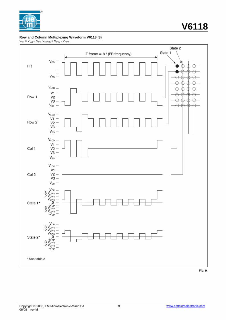
Row and Column Multiplexing Waveform V6118 (8) VOP = VLCD - VSS, VSTATE = VCOL - VROW
Fig. 9

R
V6118
Copyright © 2008, EM Microelectronic-Marin SA 06/08 – rev.M
10 www.emmicroelectronic.com
Functional Description Supply Voltage VLCD, VDD, VSS The voltage between VDD and VSS is the supply voltage for the logic and the interface. The voltage between VLCD and VSS is the supply voltage for the LCD and is used for the generation of the internal LCD bias levels. The internal LCD bias levels have a maximum impedance of 25 kΩ for a VLCD voltage from 3 to 8V. Without external connections to the V1, V2, V3 bias level inputs, the V6118 can drive most medium sized LCD (pixel area up to 4'000 mm2). For displays with a wide variation in pixel sizes, the configuration shown in Fig. 13 can give enhanced contrast by giving faster pixel switching times. On changing the row polarity (see Fig. 7, 8 and 9) the parallel capacitors lower the impedance of the bias level generation to the peak current, giving faster pixel charge times and thus a higher RMS "on" value. A higher RMS "on" value can give better contrast. IF for a given LCD size and operating voltage, the "off" pixels appear "on", or there is poor contrast, then an external bias level generation circuit can be used with the V6118. An external bias generation circuit can lower the bias level impedance and hence improve the LCD contrast (see Fig. 12). The optimum values of R, Rx and C, vary according to the LCD size used and VLCD. They are best determined through actual experimentation with the LCD. For LCD with very large average pixel area (eg. up to 10'000 mm2), the bias level configuration shown in Fig. 14 should be used. When V6118s are cascaded, connect the V1, V2 and V3 bias inputs as shown in Fig. 10. The pixel load is averaged across all the cascaded drivers. This will give enhanced display contrast as the effective bias level source impedance is the parallel combination of the total number of drivers. For example, if two V6118 are cascaded as shown in Fig. 10, then the maximum bias level impedance becomes 12.5 kΩ for a VLCD voltage from 3 to 8V. Table 8 shows the relationship between V1, V2 and V3 for the multiplex rates 2, 4 and 8. Note that VLCD > V1 > V2 > V3 for the V6118 2 and V6118 8, and for the V6118 4, VLCD > V1 > V2.
Data Input /Output The data input pin, DI, is used to load serial data into the V6118. The serial data word length is 40 bits when COL is inactive, and 48 bits when it is active. Data is loaded in inverse numerical order, the data for bit 40 (bit 48 when COL is active) loaded first with the data for bit 1 last. The column data bits are loaded first and then the address bits (see Fig. 4 & 5). The data output pin, DO, is used in cascaded applications (see Fig. 10). DO transfers the data to the next cascaded chip. The data at DO is equal to the data at DI delayed by 40 clock periods, when COL is inactive and 48 clock periods when COL is active. In order to cascade V6118s, the DO of one chip must be connected to DI of the following chip (see Fig. 10). In cascaded applications the data for the last V6118 (the one that does not have DO connected) must be loaded first and the data for the first V6118 (its DI is connected to the processor) loaded last (see Fig. 10). The display RAM word length is 40 bits (see Fig. 6). Each LCD row has a corresponding display RAM address which provides the column data (on or off) when the row is selected (on). When downloading data to the V6118, any display selected RAM address can be chosen, there is no
display RAM addressing sequence (see Fig.4 & 5). The same data can be written to more than one display RAM address. I fmore than one address bit is set, then more than one display RAM address is write enabled, and so the same data is written to more the one address. This feature can be useful to flash the LCD on and off under software control. If the address bits are all zero then no display RAM address is write enabled and no data is written to the display RAM on the falling edge of STR. Use address 0 to synchronize cascaded V6118s without updating the display RAM.
CLK Input The CLK input is used to clock the DI serial data into the shift register and to clock the DO serial data out. Loading and shifting of the data occurs at the falling edge of this clock, outputting of the data at the rising edge (see Fig. 3). When cascading devices, all CLK lines should be tied together (see Fig. 10).
STR Input The STR input is used to write to the display RAM, to blank the LCD, and synchronize cascaded V6118. The STR input writes the data loaded into the shift register, on the DI input, to the display selected RAM on the falling edge of the STR signal. The display RAM address is given by the address bits (see Fig. 4 & 5) The STR input when high blanks the LCD by disconnecting the internal voltage bias generation from the VSS potential. Segment outputs S1 to S40 (rows and columns) are pulled up to VLCD. The delay to driving the LCD with VLCD on S1 to S40, is dependent on the capacitive load of the LCD and is typically 1 µs. An LCD pixel responds to RMS voltage and takes approximately 100 ms to turn on or off. The delay from putting STR high to the LCD being blank is dependent on the LCD off time and is typically 100 ms. In applications which have a long STR pulse width (10 µs) the LCD is driven by VLCD on both the rows and columns during this time. As the time is short (1 µs), it will have zero measurable effect on the RMS "on" value (over 100 ms) of an LCD pixel and also zero measurable effect on the pixel DC component. Such STR pulses will not be visible to the human eye on an LCD. Note: if an external voltage bias generation circuit is used as shown in Fig. 12 to 14, the LCD blank function (STR high) will not blank the LCD. When STR is high, the LCD will be driven by the parallel combination of the external voltage bias generation circuit and part of the internal voltage bias generation circuit. The STR input, when high, synchronizes cascaded V6118s by forcing a new time frame to begin at the next falling edge of the FR input final (see Fig.6). A time frame begins with row 1 and so the LCD picture is rebuilt from row 1 each time cascaded V6118s are synchronized. When cascading devices, all STR lines must be tied together (see Fig. 10).
FR Input The FR signal controls the segment output frequency generation (see Fig. 7, 8 and 9). To avoid having DC on the display, the FR signal must have a 50% duty cycle. The frequency of the FR signal must be n times the desired display refresh rate, where n is the V6118 version no. (2, 4 or 8). For example, if the desired refresh rate is 40 Hz, the FR signal frequency must be 320 Hz for the V6118 8. A selected row (on) is in phasewith the FR signal (see Fig. 7, 8 and 9).
R
V6118
Copyright © 2008, EM Microelectronic-Marin SA 06/08 – rev.M
11 www.emmicroelectronic.com
It is recommended that data transfer to the V6118 should be synchronized to the FR signal to avoid a falling or rising edge on the FR signal while writing data to the V6118. The LCD pixels change polarity with the FR signal. On the edges of the FR signal current spikes will appear on the VSS and VLCD supply lines. If the supply lines have high impedance then voltage spikes will appear. These voltage spikes could interfere with data loading on the DI and CLK pins. Driver Outputs S1 to S40 There are 40 LCD driver outputs on the V6118. When COL is inactive, the outputs S1 to Sn function as row drivers and the outputs S(n+1) to S40 function as column drivers, where n is the V6118 version no. (2, 4 or 8). When COL is active, all 40 outputs function as column drivers (see Table 6). There is a one to one relationship between the display selected RAM and the LCD driver outputs. Each pixel (segment) driven by the V6118 on the LCD has a display RAM bit which corresponds to it. Setting the bit turns the segment "on" and clearing it turns it "off".
COL Input The V6118 functions as a row and column driver while the COL input is inactive. When active, the COL input configures the V6118 to function as a column driver only. The former row outputs function as column outputs. In cascaded applications, one V6118 should be used in the row and column configuration ( COL inactive) and the rest as pure column drivers ( COL active) (see Fig. 10). Note: when cascading V6118s never cascade one version with another. If a V6118 8 is used to drive the rows, then only V6118 8 can be cascaded with it. When COL is active the V6118 needs 48 bits of data in a load cycle . 40 bits are used for the column data and 8 bits to address the display RAM regardless of V6118 versions (2, 4or 8) (see Fig.4, 5 and 10) Power Up On power up the data in the shift registers, the two display RAMs and the 40 bit display latches are undefined. The STR input should be taken high on power up to blank the display, then the display data written to the display selected RAM (see Fig. 11). When finished the initial write to the display selected RAM, take the STR input low to display the display selected RAM contents (see also section "STR Input").
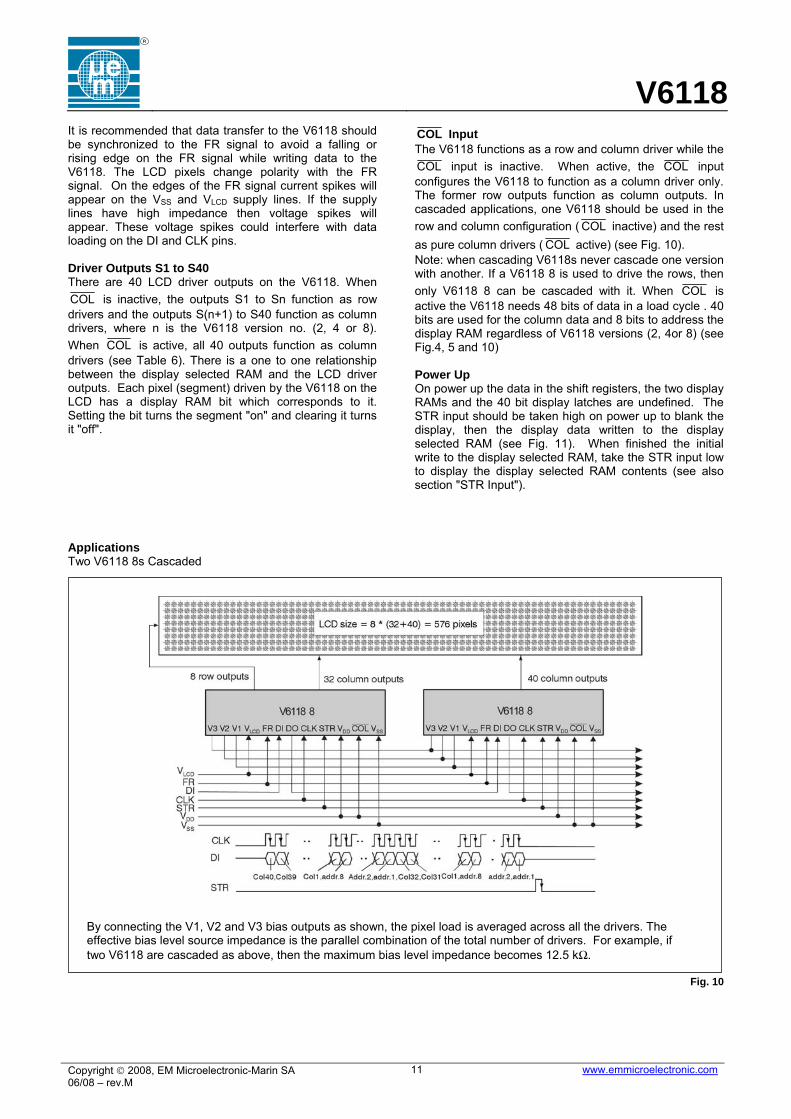
Applications Two V6118 8s Cascaded
By connecting the V1, V2 and V3 bias outputs as shown, the pixel load is averaged across all the drivers. The effective bias level source impedance is the parallel combination of the total number of drivers. For example, if two V6118 are cascaded as above, then the maximum bias level impedance becomes 12.5 kΩ.
Fig. 10

R
V6118
Copyright © 2008, EM Microelectronic-Marin SA 06/08 – rev.M
12 www.emmicroelectronic.com
Microprocessor Interface and LCD Blanking
1) When the microprocessor is reset, the port pin will be configured as an input and so the STR line would float. The pull-up resistor will ensure that the LCD is blank while the system reset line is active and after until the port pin is set up by software.
Writing Data to the Display RAM while keeping the LCD Blank
Fig. 11 V6118 with External Resistor Divider Bias Generation
Example set values: R = 3.3 – 10 kΩ C = 2.2 – 47 nF Rx is given by the formula: Rx = 4R ((VDISP/VLCD)-1) = 10 – 30 kΩ
Fig. 12

R
V6118
Copyright © 2008, EM Microelectronic-Marin SA 06/08 – rev.M
13 www.emmicroelectronic.com
Enhanced Switching from V6118
C = 1µF Rx is given by the formula Rx = 4(24 kΩ) ((VDISP/VLCD) -1)
Fig.13
Bias configuration for a large LCD
Large LCD example: VOP = 5V, average pixel active area = up to 10'000 mm2, display refresh rate = 64 Hz For a single V6118 4 driving of such an LCD, the voltage follower buffer (opamp) requirement is: peak current 1.8 mA steady state current typically 100 µA Fig.14
Package and Ordering Information Dimensions of TAB Package
All dimensions in mm
Fig.15

R
V6118
Copyright © 2008, EM Microelectronic-Marin SA 06/08 – rev.M
14 www.emmicroelectronic.com
Dimensions of QFP Package
All dimensions in mm
Fig.16

R
V6118
Copyright © 2008, EM Microelectronic-Marin SA 06/08 – rev.M
15 www.emmicroelectronic.com
Package and Ordering Information Dimensions of Chip Form
Thickness (typ.) = 11 mils Chip size is X = 3657 by Y = 2895 microns or X = 144 by Y = 114 mils Note: The origin (0,0) is the lower left coordinate of center pads The lower left corner of the chip shows the distances to the origin All dimensions in micron
Fig. 17
Ordering Information The V6118 is available in the following packages:
QFP52, pin plastic package V6118 2 52F Chip form V6118 2 Chip* V6118 4 52F V6118 4 Chip* V6118 8 52F
V6118 8 Chip*
TAB, tape automated bonding V6118 2 TAB *on request V6118 4 TAB
V6118 8 TAB When ordering, please specify the complete part number and package
EM Microelectronic-Marin SA (EM) makes no warranty for the use of its products, other than those expressly contained in the Company's standard warranty which is detailed in EM's General Terms of Sale located on the Company's web site. EM assumes no responsibility for any errors which may appear in this document, reserves the right to change devices or specifications detailed herein at any time without notice, and does not make any commitment to update the information contained herein. No licenses to patents or other intellectual property of EM are granted in connection with the sale of EM products, expressly or by implications. EM's products are not authorized for use as components in life support devices or systems.