em microelectronic - marin sa em8500 · em8500 420005-a01, 2.0 lts sts lts vsup sts sts lts
TRANSCRIPT

EM8500
Copyright 2017, EM Microelectronic-Marin SA 8500-DS, Version 2.1, 24-May-17
1 www.emmicroelectronic.com
420005-A01, 2.0
POWER MANAGEMENT CONTROLLER WITH ENERGY HARVESTING INTERFACE
Description The EM8500 is an integrated power management solution for low power applications. It is specifically designed for efficient operation with a variety of DC harvesting sources including thermal electric generators (TEG) or photovoltaic (solar) sources in the μW to mW
range. The device is designed to speed-up system start-up time when the main energy storage element (aka Long Term Storage – LTS) is completely discharged or insufficiently charged to supply the application, by using a secondary energy storage element (Short Term Storage - STS). When using a non-rechargeable primary battery the EM8500's on-board PMU offers a mechanism to extend battery life when assisted by a harvesting element. The EM8500 incorporates a boost converter able to start with an input voltage as low as 300 mV and an input power of few μW.
In functional mode the EM8500 operates at energy levels from a DC
harvesting source as low as 100 mV and 1 μW. To maximize
harvesting efficiency the EM8500 integrates a programmable maximum power point tracking controller. The EM8500 is capable of working with a variety of energy elements as secondary storage, namely re-chargeable batteries, super-capacitors or conventional capacitors. In all cases the EM8500 maintains its fast start-up capability that depends only on the harvester conditions and the STS capacitor value. A USB connection to an external power source is available on the EM8500 for fast charge of the long term storage element. The EM8500 integrates voltage supervisory functions. Minimum and maximum voltages are controlled on the LTS element to prevent damage to the energy storage element. Harvester minimum voltage monitoring allows stopping the DCDC limiting power loss when no energy can be harvested. Output voltages are kept in a safe range for the application.
To perform granular power management of the application, the EM8500 integrates four independent supply outputs and a sleep mode offering the capability to switch off part or all the supplies. The EM8500 is available in an industry standard QFN24 4x4 package or as a solder bump flip-chip device.
Features Flexible operation with different energy banks Primary cell battery Secondary cell battery Capacitors (gold-cap, super-cap)
Ultra-low power DCDC boost converter with very high efficiency Operating mode minimum voltage VDD_HRV ≥ 100 mV (typical) Operating mode minimum power: PIN ≥ 1µW (typical) Quiescent current: IQ ≤ 125 nA Cold-start minimum voltage: VIN ≥ 300 mV Cold-start minimum power: PIN ≥ 3 µW (typical)
Fast start-up on any energy storage Dual energy storage elements
Power management control Multiple independent supply outputs Sleep mode and wake-up functions User programmable under-voltage and over-voltage levels
Limited external components Device configurations are stored in on-chip E2PROM Dynamic configuration through a SPI or I2C interface
Extended power management status Battery on protection mode LTS/STS connection status Minimum/Maximum voltage warning USB connected
Applications Energy harvesting equipped platforms
Solar charging Thermo-electrical generator harvesting (TEG)
Wearable systems Beacons and wireless sensor networks Industrial and environmental monitoring Battery operated platforms
EM8500
24 23 22 21 20 19
2
1
7
VDD_USB
N.C
.
MOSI_SDA
MISO
SCL
VSUP
VAUX[2]
VAUX[1]
VA
UX
[0]
N.C.
VA
UX
_G
ND
[2]
VDD_STS
VD
D_
LT
S
LX
1
VS
S
VD
D_
HR
V
VR
EG
CS
WAKE_UP
BAT_LOW
HRV_LOW
VA
UX
_G
ND
[0]
VA
UX
_G
ND
[1]
4
3
6
5
17
18
15
16
13
14
24 Lead MLF
4x4mm body
8 9 10 11 12
VS
S_
DC
DC
Figure 1-1 QFN24 Package
EM MICROELECTRONIC - MARIN SA
EM8500
Copyright 2017, EM Microelectronic-Marin SA 8500-DS, Version 2.1, 24-May-17
2 www.emmicroelectronic.com
420005-A01, 2.0
TABLE OF CONTENTS
1. Product description ..................................................................................................................... 4
1.1. Operating modes ................................................................................................................................ 4
1.2. voltage naming conventions ............................................................................................................... 4
1.3. Block diagram .................................................................................................................................... 5
1.4. Functional description ........................................................................................................................ 6 1.4.1. Cold-start on harvester ............................................................................................................................................ 6 1.4.2. Start-up on Long Term Storage (LTS) ....................................................................................................................... 7 1.4.3. System shut-down ................................................................................................................................................... 8
2. Handling Procedures ................................................................................................................... 9
3. Pin description ............................................................................................................................ 9
4. Electrical specifications ............................................................................................................. 10
4.1. Absolute Maximum Ratings .............................................................................................................. 10
4.2. Operating Conditions ........................................................................................................................ 10
4.3. Electrical Characteristics ................................................................................................................... 10
4.4. Timing diagrams ............................................................................................................................... 12 4.4.1. SPI interface ........................................................................................................................................................... 12 4.4.2. I2C Interface ........................................................................................................................................................... 12
5. Product configuration ............................................................................................................... 12
5.1. Status information ........................................................................................................................... 12
5.2. Supervising and harvester controller behaviour ................................................................................ 13 5.2.1. Storage element ..................................................................................................................................................... 13 5.2.2. Harvester power supervisory functions ................................................................................................................. 14 5.2.3. Timing configuration .............................................................................................................................................. 15 5.2.4. Maximum Power Point tracking ............................................................................................................................. 16
5.3. Power management functions .......................................................................................................... 16
5.4. Primary cell configuration ................................................................................................................. 18
5.5. Sleep mode and Wake-up functions .................................................................................................. 19
5.6. Lux-meter ........................................................................................................................................ 19
5.7. USB charging .................................................................................................................................... 21
5.8. Miscellaneous functions ................................................................................................................... 21 5.8.1. Soft reset function ................................................................................................................................................. 21 5.8.2. Register protection ................................................................................................................................................ 22 5.8.3. LTS protection DISABLE .......................................................................................................................................... 22 5.8.4. DCDC off forcing ..................................................................................................................................................... 22
6. Serial interface .......................................................................................................................... 22
6.1. I2C interface ..................................................................................................................................... 22
6.2. SPI interface ..................................................................................................................................... 23 6.2.1. Interface selection ................................................................................................................................................. 24
6.3. E2PROM ........................................................................................................................................... 24 6.3.1. Accessing the E2PROM .......................................................................................................................................... 24

EM8500
Copyright 2017, EM Microelectronic-Marin SA 8500-DS, Version 2.1, 24-May-17
3 www.emmicroelectronic.com
420005-A01, 2.0
7. Typical characteristics ............................................................................................................... 27
8. Register map ............................................................................................................................. 28
9. Typical Applications .................................................................................................................. 31
9.1. SAMPLE schematics .......................................................................................................................... 31 9.1.1. Solar cell assisted system ....................................................................................................................................... 31 9.1.2. termo-electrical generator (TEG) assisted system ................................................................................................. 32
9.2. Inductor selection............................................................................................................................. 32 9.2.1. Reference Inductors ............................................................................................................................................... 32
9.3. Capacitor selection ........................................................................................................................... 33
10. Ordering Information .............................................................................................................. 33
11. Package Information .............................................................................................................. 33
11.1. QFN24 4x4 package ....................................................................................................................... 33 11.1.1. Package marking .................................................................................................................................................... 33

EM8500
Copyright 2017, EM Microelectronic-Marin SA 8500-DS, Version 2.1, 24-May-17
4 www.emmicroelectronic.com
420005-A01, 2.0
1. PRODUCT DESCRIPTION
The EM8500 is a power management IC with battery charger functions. It manages different energy source elements: a harvester through VDD_HRV, external supply through VDD_USB, a battery or a Long Term Storage (LTS) through VDD_LTS. It generates a local supply on a Short Term Storage (STS), visible through VDD_STS. The EM8500 provides the supply to the application from the energy sources. Surplus energy is stored in a LTS element.
Features and benefits include:
Power management controller, extending application battery life: the EM8500 supplies the external application through the pins VSUP and VAUX[i]. The voltage is delivered directly from VDD_STS or through a regulator. On the VSUP pin a wake-up function allows to automatically re-enable the supply after a given time. For external devices using an I2C serial interface, it is possible to disconnect their ground through the use of the auxiliary ground pins (VAUX_GND). This solution avoids supplying the devices connected to a switched-off output supply through the pull-up of I2C bus. Overall power consumption is reduced by turning off peripheral ICs through the EM8500.
Battery charger from harvester source: EM8500 manages energy harvesting from a low voltage and low power DC source such as single/dual junction solar cells or thermal electrical generator (TEG). The device embeds hardware MPPT (Maximum Power Point Tracking) algorithm to extract maximum energy from the harvester element. The DCDC boost converter is able to start the application from the harvester source. With its dual storage architecture, application start-up is fast and independent of the battery voltage.
Battery charger from USB source : Fast charging is supported through a USB compatible supply input on the EM8500 (system start-up and battery charging to maximum voltage with configurable speed).
Voltage and current supervisor: The EM8500 includes supervisory functions to detect harvester energy levels detecting (visible through the HRV_LOW pin) – and to monitor low battery voltage levels (visible through the BAT_LOW pin). The EM8500 protects the battery against over voltage conditions and automatically stops charging when a configurable threshold level is reached.
Configuration with E2PROM, no additional external components: The mode and functional configuration of the EM8500 is controlled by the host MCU through a SPI or an I2C interface. Voltage supervision thresholds are set by registers. Configuration parameters are held in on-chip non-volatile memory (E2PROM). The EM8500 default configuration parameter values can be modified by the user.
1.1. OPERATING MODES
The EM8500 operates in three main modes:
1) Normal mode (STS and LTS Connected) - VLTS is inside battery operating range. - LTS is connected to STS. - The system can be configured to disconnect VAUX or/and VAUX_GND pins.
2) LTS protection mode (STS and LTS disconnected)
- EM8500 enters this mode when VLTS drops below minimum battery operation (v_bat_min_lo). - BAT_LOW pin is set to '1'. - LTS and STS are disconnected to protect LTS against under voltage condition. - VSUP and VAUX are maintained through the DCDC converter only.
3) Sleep mode
- VSUP is not supplied – no communication on SPI/I2C interface. - VSUP can be re-activated by WAKE_UP pin or internal timer.
1.2. VOLTAGE NAMING CONVENTIONS
To describe the operation of this product, the following set of voltage naming conventions is adopted throughout this document , Table 1-1:
NAME DESCRIPTION
v_bat_max_hi Maximum battery voltage. High level of hysteresis. v_bat_min_hi_dis Minimum STS maintenance voltage – acts as v_bat_min_hi when STS and LTS are disconnected
v_bat_min_hi_con Minimum battery maintenance voltage – acts as v_bat_min_hi when STS and LTS are connected
v_bat_min_hi Minimum battery voltage. High level of hysteresis Equal to v_bat_min_hi_dis or v_bat_min_hi_con according to the connection state in between STS and LTS. The term “v_bat_min_hi” is used here whenever there is no specific usage of the connected and disconnected values
v_bat_min_lo Minimum battery voltage. Low level of hysteresis
v_apl_max_hi Maximum application voltage. High level of hysteresis
v_apl_max_lo Maximum application voltage. Low level of hysteresis
Vcs_hi Cold start voltage level v_ulp_ldo Regulated voltage on VSUP pin
v_hrv_min Minimum voltage for switching on/off the DCDC. See §5.2.2 for current or voltage detection selection.
Table 1-1 Voltage Naming Conventions

EM8500
Copyright 2017, EM Microelectronic-Marin SA 8500-DS, Version 2.1, 24-May-17
5 www.emmicroelectronic.com
420005-A01, 2.0
1.3. BLOCK DIAGRAM
EM
85
00
LX
1
VD
D_
HR
V
VD
D_
LT
S
VS
UP
CS
HR
V_L
OW
SC
L
CH
RV
Ba
tte
ry (
or
su
pe
r-ca
pa
cito
r)
L1
MO
SI_
SD
A
VD
D_
ST
S
CS
TS
UL
P L
DO
sw_lts_sts
sw
_vd
cd
c_
lts_
sts
_n
BA
T_L
OW
VA
UX
_G
ND
[0]
VA
UX
_G
ND
[1]
VA
UX
_G
ND
[2]
VS
S
VD
D_U
SB
US
B
5V
ch
arg
ing
VR
EG
Cre
g
WA
KE
_U
P
MIS
O
DC
DC
MP
PT
Co
ntr
olle
r
Bo
ost
Co
ntr
olle
r
Co
ld-s
tart
bo
oste
r
VA
UX
[0]
VA
UX
[1]
VA
UX
[2]
VS
UP
Sle
ep
co
un
ter
Ap
plic
ati
on
Su
pp
ly
co
ntr
ol
HR
V c
urr
en
t
me
asu
rem
en
t
aka
lu
x-m
ete
r
I2C
or
SP
I
inte
rfa
ce
de-b
ou
nce
r
Re
gis
ters
E2P
RO
M(d
efa
ult v
alu
es)
VS
S_
DC
DC
LD
O
ST
S/L
TS
/
HR
V
su
pe
rvis
ory
Ha
rve
ste
r
(TE
G o
r S
ola
r)
Co
ntr
ol
Un
it
Application
CL
TS
Inte
rna
l su
pp
ly
reg
ula
tor
Figure 1-1 EM8500 Block Diagram

EM8500
Copyright 2017, EM Microelectronic-Marin SA 8500-DS, Version 2.1, 24-May-17
6 www.emmicroelectronic.com
420005-A01, 2.0
1.4. FUNCTIONAL DESCRIPTION
The following paragraphs describe the behavior of VSTS, VLTS and VSUP for a series of typical use cases;
(VAUX supplies have the same behavior as VSUP).
1.4.1. COLD-START ON HARVESTER
This use case outlines a start-up on harvester voltage, with all storage elements discharged or in protection mode.
t
VSTS
VLTS
VSUP
Vcs_hi
v_apl_max_lo
v_apl_max_hi
v_ulp_ldo
v_bat_max_hi
v_bat_max_lo
STS LTSVSUP
1 2 3
v_bat_min_hi
v_bat_min_lo
tHRV_LOW
BAT_LOW
4 5 4 6
Figure 1-2 Start-up and energy storage sequence when LTS is lower than the cold-start voltage
1. The DCDC starts transferring energy from HRV to STS 2. When VSTS is higher than Vcs_hi, the cold start sequences ends, the device boots and the DCDC is switched to main charging mode
with MPPT tracking. 3. When VSTS rises above v_bat_min_hi, VSUP is connected to STS supplying the application 4. When VSTS reaches the maximum application voltage level v_apl_max_lo, the DCDC transfers energy into LTS. The application is
supplied by the CSTS only. 5. When VSTS drops to the minimum pre-defined charge value v_bat_min_hi, the DCDC transfers energy back into STS 6. The system remains in states 4 & 5 until VLTS is higher than the minimum battery voltage required to supply the external application
v_bat_min_hi. Then LTS is connected to STS and both storage elements are charged in parallel. The output BAT_LOW is set to '0'.
EM8500
Copyright 2017, EM Microelectronic-Marin SA 8500-DS, Version 2.1, 24-May-17
7 www.emmicroelectronic.com
420005-A01, 2.0
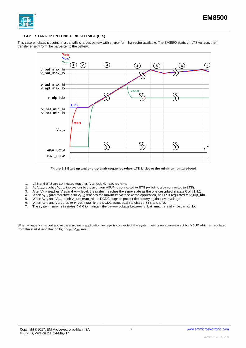
1.4.2. START-UP ON LONG TERM STORAGE (LTS)
This case emulates plugging in a partially charges battery with energy form harvester available. The EM8500 starts on LTS voltage, then transfer energy form the harvester to the battery.
t
v_apl_max_lo
v_apl_max_hi
v_ulp_ldo
v_bat_max_hi
v_bat_max_lo
STS
LTS
VSUP
1 5
v_bat_min_hi
v_bat_min_lo
Vcs_hi
VSTS
VLTS
VSUP
tHRV_LOW
BAT_LOW
2 3 4 5 6
Figure 1-3 Start-up and energy bank sequence when LTS is above the minimum battery level
1. LTS and STS are connected together, VSTS quickly reaches VLTS. 2. As VSTS reaches Vcs_hi, the system boots and then VSUP is connected to STS (which is also connected to LTS). 3. After VSUP reaches VLTS and VSTS level, the system reaches the same state as the one described in state 6 of §1.4.1 4. When VLTS (and therefore also VSTS) reaches the maximum voltage of the application, VSUP is regulated to v_ulp_ldo. 5. When VLTS and VSTS reach v_bat_max_hi the DCDC stops to protect the battery against over voltage 6. When VLTS and VSTS drop to v_bat_max_lo the DCDC starts again to charge STS and LTS. 7. The system remains in states 5 & 6 to maintain the battery voltage between v_bat_max_hi and v_bat_max_lo.
When a battery charged above the maximum application voltage is connected, the system reacts as above except for VSUP which is regulated from the start due to the too high VSTS/VLTS level.
EM8500
Copyright 2017, EM Microelectronic-Marin SA 8500-DS, Version 2.1, 24-May-17
8 www.emmicroelectronic.com
420005-A01, 2.0
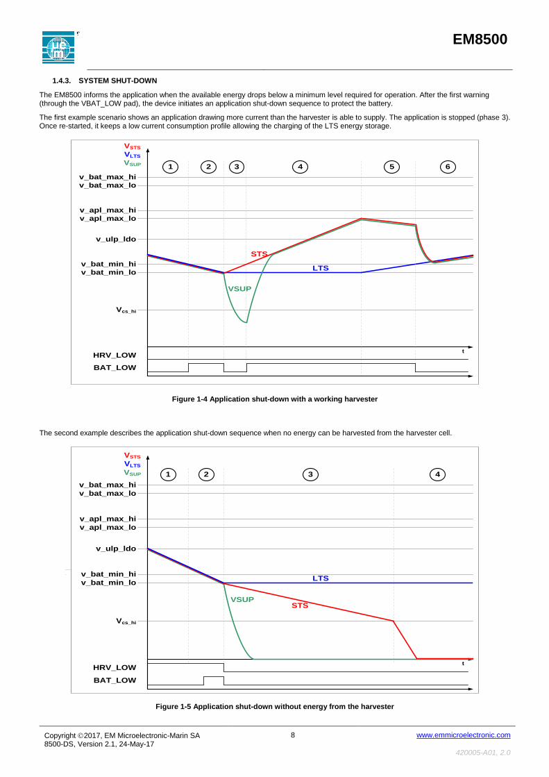
1.4.3. SYSTEM SHUT-DOWN
The EM8500 informs the application when the available energy drops below a minimum level required for operation. After the first warning (through the VBAT_LOW pad), the device initiates an application shut-down sequence to protect the battery.
The first example scenario shows an application drawing more current than the harvester is able to supply. The application is stopped (phase 3). Once re-started, it keeps a low current consumption profile allowing the charging of the LTS energy storage.
t
VSTS
VLTS
VSUP
Vcs_hi
v_apl_max_lo
v_apl_max_hi
v_ulp_ldo
v_bat_max_hi
v_bat_max_lo
STS
LTS
VSUP
1 3 4 5 6
v_bat_min_hi
v_bat_min_lo
2
tHRV_LOW
BAT_LOW
Figure 1-4 Application shut-down with a working harvester
The second example describes the application shut-down sequence when no energy can be harvested from the harvester cell.
t
VSTS
VLTS
VSUP
Vcs_hi
v_apl_max_lo
v_apl_max_hi
v_ulp_ldo
v_bat_max_hi
v_bat_max_lo
STS
LTS
VSUP
1 3 4
v_bat_min_hi
v_bat_min_lo
2
tHRV_LOW
BAT_LOW
Figure 1-5 Application shut-down without energy from the harvester
EM8500
Copyright 2017, EM Microelectronic-Marin SA 8500-DS, Version 2.1, 24-May-17
9 www.emmicroelectronic.com
420005-A01, 2.0
2. HANDLING PROCEDURES
This device has built-in protection against high static voltages or electric fields; however, anti-static precautions must be taken as for any other CMOS component. Unless otherwise specified, proper operation can only occur when all terminal voltages are kept within the voltage range. Unused inputs must always be tied to a defined logic voltage level.
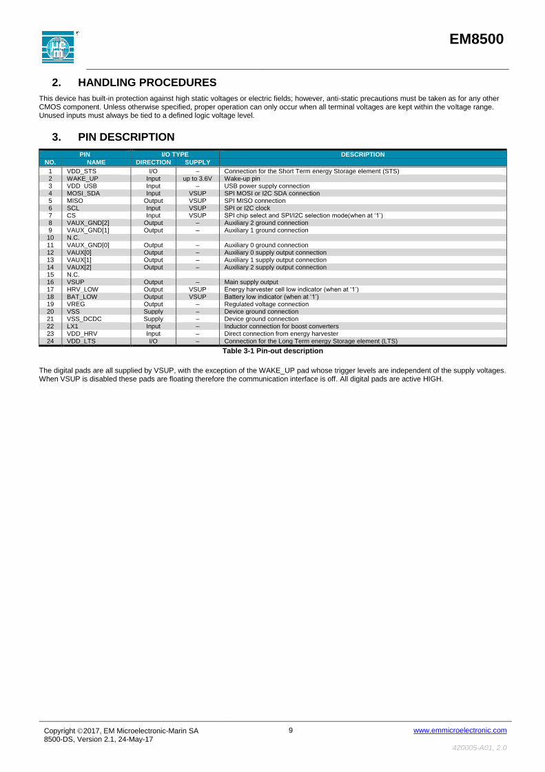
3. PIN DESCRIPTION
PIN I/O TYPE DESCRIPTION
NO. NAME DIRECTION SUPPLY
1 VDD_STS I/O – Connection for the Short Term energy Storage element (STS) 2 WAKE_UP Input up to 3.6V Wake-up pin 3 VDD_USB Input – USB power supply connection 4 MOSI_SDA Input VSUP SPI MOSI or I2C SDA connection 5 MISO Output VSUP SPI MISO connection 6 SCL Input VSUP SPI or I2C clock 7 CS Input VSUP SPI chip select and SPI/I2C selection mode(when at ‘1’) 8 VAUX_GND[2] Output – Auxiliary 2 ground connection 9 VAUX_GND[1] Output – Auxiliary 1 ground connection 10 N.C.
11 VAUX_GND[0] Output – Auxiliary 0 ground connection 12 VAUX[0] Output – Auxiliary 0 supply output connection 13 VAUX[1] Output – Auxiliary 1 supply output connection 14 VAUX[2] Output – Auxiliary 2 supply output connection 15 N.C. 16 VSUP Output – Main supply output 17 HRV_LOW Output VSUP Energy harvester cell low indicator (when at ‘1’) 18 BAT_LOW Output VSUP Battery low indicator (when at ‘1’) 19 VREG Output – Regulated voltage connection 20 VSS Supply – Device ground connection 21 VSS_DCDC Supply – Device ground connection 22 LX1 Input – Inductor connection for boost converters 23 VDD_HRV Input – Direct connection from energy harvester 24 VDD_LTS I/O – Connection for the Long Term energy Storage element (LTS)
Table 3-1 Pin-out description
The digital pads are all supplied by VSUP, with the exception of the WAKE_UP pad whose trigger levels are independent of the supply voltages. When VSUP is disabled these pads are floating therefore the communication interface is off. All digital pads are active HIGH.
EM8500
Copyright 2017, EM Microelectronic-Marin SA 8500-DS, Version 2.1, 24-May-17
10 www.emmicroelectronic.com
420005-A01, 2.0
4. ELECTRICAL SPECIFICATIONS
4.1. ABSOLUTE MAXIMUM RATINGS
PARAMETER VALUE UNIT
MIN MAX
Power supply VDD_HRV -0.2 2.0 V Power supply VDD_STS, VDD_LTS -0.2 4.6 V Power supply VDD_USB -0.2 6.0 V Input voltage VSS-0.2 VSUP+0.2 V Input voltage (pin WAKE_UP) -0.2 3.8 V Storage Temperature Range (TSTG) -65 150 °C Electrostatic discharge to ANSI/ESDA/JEDEC JS-001-2012 for HBM -2000 2000 V
Table 4-1 Absolute maximum ratings
Stresses above these listed maximum ratings may cause permanent damages to the device. Exposure beyond specified operating conditions may affect device reliability or cause malfunction.
Warning: The device is not functional when exposed to light. When a non-packaged version is used, it is mandatory to protect the device from light (e.g. glob-top, non-transparent package, metal shield on the PCB …)
4.2. OPERATING CONDITIONS
PARAMETER SYMBOL MIN TYP MAX UNIT
DC input voltage into VDD_HRV(1) VHRV 0.1 0.5 1.8 V Long Term energy Storage bank voltage VLTS 3.0 4.2 V Short Term energy Storage bank voltage VSTS 3.0 4.2 V VDD_USB voltage VUSB 5 5.5 V Long term capacitor(2) CLTS 0.001 2 F Short term capacitor CSTS 10 47 µF Regulated voltage capacitor CREG 470 nF Harvester capacitor (nominal value) CHRV 4.7 10 µF VSUP capacitor CSUP 1 0.1*CSTS µF VAUX capacitor CAUX 1 0.1*CSTS µF Input inductance L1 37.6 47 56.4 µH
(1) Cold-start has been completed (2) When using a super-capacitor
Table 4-2 Operating Conditions
4.3. ELECTRICAL CHARACTERISTICS
Unless otherwise specified: TA=-40 to +85°C for min max specifications and TA= 25°C for typical specifications.
PARAMETER SYMBOL CONDITIONS MIN TYP MAX UNIT End of cold-start Voltage on VDD_STS Vcs_hi With VSTS increasing 1.3 V Start of cold-start Voltage on VDD_STS Vcs_lo With VSTS decreasing 1.1 V Typical DC input voltage range into VDD_HRV Cold-start completed 0.1 1.8 V Typical input power range VSTS > Vcs_hi VVDD_HRV = 0.5V 0.001 100 mW Minimum cold-start voltage for charging STS VSTS < Vcs_lo 300 1800 mV Minimum cold-start input power VSTS < Vcs_lo 3 µW Cold-start duration CSTS = 47uF, VHRV = 0.5V, PHRV = 100µW, VSTS(0s)=0V,
VLTS(0s)=0V, v_bat_min_hi=2V 2 s
CURRENT CONSUMPTIONS ON LTS IDD in “LTS protection mode” and “HRV low mode”
ILTS_prot1 Battery supervisory at 4Hz; VSUP and VAUX LDOs disabled 65 nA
IDD in “LTS protection mode” ILTS_prot2 Battery supervisory at 4Hz; VSUP and VAUX LDOs disabled 15 nA IDD in “HRV low mode” STS and LTS connected IHRV_lo2 Battery supervisory at 4Hz; VSUP and VAUX LDOs disabled 145 nA IDD in “HRV low mode” STS and LTS connected IHRV_lo3 Battery supervisory at 4Hz; ULP LDO enabled and VAUX LDO
disabled 170 nA
IDD in “HRV low mode” STS and LTS connected IHRV_lo4 Battery supervisory at 4Hz; VSUP and VAUX[0] LDO enabled 285 nA IDD in “HRV low mode” STS and LTS connected IHRV_lo5 Battery supervisory at 4Hz; VSUP and VAUX[1] LDO enabled 265 nA IDD in “HRV low mode” STS and LTS connected IHRV_lo6 Battery supervisory at 4Hz; VSUP and VAUX[2] LDO enabled 250 nA IDD in “HRV low mode” STS and LTS connected IHRV_lo6 Battery supervisory at 4Hz; VSUP and all VAUX LDO enabled 380 nA IDD in “normal mode” STS and LTS disconnected
INORM Battery supervisory at 4Hz; VSUP and VAUX LDOs disabled (VDD_STS < VDD_LTS)
45 nA
QUIESCENT CURRENT AND LEAKAGE ON STS (WHEN LTS IS NOT CONNECTED TO STS) IDD in “HRV low mode” ISTS_hrvlo Battery supervisory at 4Hz; VSUP and VAUX LDOs disabled 65 nA
VSUP AND VAUX LDO VOLTAGE LEVEL ULP/VAUX LDO level 0 VSTS – VSUP> 0.3V 1.08 1.2 1.32 V ULP/VAUX LDO level 1 VSTS – VSUP> 0.3V 1.39 1.55 1.71 V ULP/VAUX LDO level 2 VSTS – VSUP> 0.3V 1.48 1.65 1.82 V ULP/VAUX LDO level 3 VSTS – VSUP> 0.3V 1.62 1.8 1.98 V ULP/VAUX LDO level 4 VSTS – VSUP> 0.3V 1.8 2 2.2 V ULP/VAUX LDO level 5 VSTS – VSUP> 0.3V 1.98 2.2 2.42 V ULP/VAUX LDO level 6 VSTS – VSUP> 0.3V 2.16 2.4 2.64 V ULP/VAUX LDO level 7 VSTS – VSUP> 0.3V 2.34 2.6 2.86 V
MAXIMUM CURRENT ON THE ULP AND VAUX LDO Maximum current on ULP LDO Drop from open voltage is 100 mV, LDO level at 1.8V 10 mA Maximum current on VAUX[0] LDO Drop from open voltage is 100 mV, LDO level at 1.8V 20 mA Maximum current on VAUX[1] LDO Drop from open voltage is 100 mV, LDO level at 1.8V 10 mA Maximum current on VAUX[2] LDO Drop from open voltage is 100 mV, LDO level at 1.8V 5 mA
SWITCH RESISTOR VDD_LTS to VDD_STS Rsw_LTS_STS VDD_STS at 3V 3.1 Ω VDD_STS to VSUP Rsw_VSUP VDD_STS at 3V 7.4 Ω VDD_STS to VAUX[0]
Rsw_VAUX0 VDD_STS at 3V 4.4 Ω
VDD_STS to VAUX[1] Rsw_VAUX1 VDD_STS at 3V 5.8 Ω

EM8500
Copyright 2017, EM Microelectronic-Marin SA 8500-DS, Version 2.1, 24-May-17
11 www.emmicroelectronic.com
420005-A01, 2.0
PARAMETER SYMBOL CONDITIONS MIN TYP MAX UNIT VDD_STS to VAUX[2]
Rsw_VAUX2 VDD_STS at 3V 6.4 Ω
VAUX_GND[0] to VSS Rsw_GND0 VDD_STS at 3V 4.74 Ω
VAUX_GND[1,2] to VSS Rsw_GND1,2 VDD_STS at 3V 5.62 Ω
SUPERVISORY LEVELS ON STS, LTS AND HRV(1) Maximum voltage 4.2 V Level step from lvl0 to lvl15 Vlvl_15 73 mV Level step from lvl16 to lvl30 (1.24V to 2.26V) Vlvl_30 67.9 73 78.1 mV Level step from lvl31 to lvl54 (2.34V to 4.2V) Vlvl_54 69.4 73 76.7 mV Differential non linearity ±0.5 LSB Number of levels 54
HARVESTER CURRENT LEVEL DETECTOR – LUX METER Harvester current level step Ihrv_check_lvl 1 µA Luxmeter current detection level “lvl” = level used for the measurement [0..15]
Ilux_lvl 2lvl µA
Short circuit voltage Vhrv_scv 70 mV
USB POWER Minimum voltage for USB charging detection Vusb_min 3.5 V Regulated voltage on VDD_STS VUSB_REG 2.1 V Current source level 0 on LTS IUSB_lvl0 0 mA Current source level 1 on LTS IUSB_lvl1 6.9 mA Current source level 2 on LTS IUSB_lvl2 12.7 mA Current source level 3 on LTS IUSB_lvl3 20.6 mA
E2PROM PARAMETERS E2PROM write time Tee_wr 8 ms E2PROM read time Tee_rd 0.9 ms E2PROM maximum write cycle Nee_cyc 1000 E2PROM read hold time Thd_rd 10 µs
INTERFACE PARAMETERS Input WAKE_UP - low level Vil_wk VLTS=1.2V to 3.6V 0.3 V Input WAKE_UP - high level Vih_wk VLTS =1.2V to 3.6V 0.9 V Wake-up rising edge reaction time Tr_wk Debouncer disabled 4.5 µs Wake-up falling edge reaction time Tf_wk Debouncer disabled 120 µs Input - low level Vil_si VSUP=1.2V to 3.6V 0.2*
VSUP V
Input - high level Vih_si VSUP =1.2V to 3.6V 0.8* VSUP
V
Output – low level for I2C(3) Iol_sda VSUP =1.8V, Vol=0.2* VSUP 3 mA Output – low level for I2C Iol_sda_1.2 VSUP =1.20V, Vol=0.23*Vsup 3 mA Output – low level(3) Iol VSUP =1.8V, Vol=0.2*Vsup
(MISO, MOSI_SDA, BAT_LOW, HRV_LOW) 1 mA
Output – low level Iol_1.2 VSUP =1.20V, Vol=0.23*Vsup (MISO, MOSI_SDA, BAT_LOW, HRV_LOW)
1 mA
Output – high level(3) Ioh VSUP =1.8V, Voh=0.8*Vsup (MISO, MOSI_SDA, BAT_LOW, HRV_LOW)
-1 mA
Output – high level Ioh_1.2 VSUP =1.2V, Voh=0.8*Vsup (MISO, MOSI_SDA, BAT_LOW, HRV_LOW)
-1 mA
I2C bus load capacitor Cb On MOSI_SDA and SCL 400 pF
SPI TIMINGS SPI clock input frequency Fspi 5 MHz SCL low pulse Tlow_scl 20 ns SCL high pulse Thigh_scl 20 ns MOSI_SDA setup time Tsetup_mosi 20 ns MOSI_SDA hold time Thold_mosi 20 ns MISO output delay Tdelay_miso 25pF load, VSUP =1.6V min 30 ns MISO output delay Tdelay_miso 25pF load, VSUP =1.2V min 40 ns CS setup time Tsetup_cs 50 ns CS hold time Thold_cs 20 ns I2C TIMINGS(2) MOSI_SDA setup time tsudat Standard & Fast Modes 160 ns
High Speed Mode 30 ns MOSI_SDA hold time thddat Standard & Fast Modes with Cb =100pF Max. 80 ns
Standard & Fast Modes with Cb =400pF Max 90 ns High Speed Mode with Cb=100pF Max. 18 115 ns High Speed Mode with Cb=400pF Max. 24 150 ns
SCL low pulse(3) tlow High Speed Mode with Cb=100pF Max. VSUP =1.8V
160 ns
SCL low pulse tlow High Speed Mode with Cb=100pF Max. VSUP =1.2V 210 ns
(1) The v_bat_min, v_bat_max, v_apl_min with their hysteresis can be set according to the supervising levels. E.g. for v_bat_max, both v_bat_max_lo and v_bat_max_hi will have to be set accordingly.
(2) Refers to I2C specification 2.1 (January 2000) (3) When reg_ext_cfg.sdi_slope_ctrl = ‘1’
Table 4-3 Electrical Specifications
EM8500
Copyright 2017, EM Microelectronic-Marin SA 8500-DS, Version 2.1, 24-May-17
12 www.emmicroelectronic.com
420005-A01, 2.0
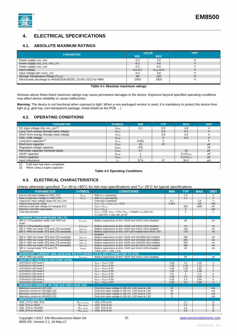
4.4. TIMING DIAGRAMS
4.4.1. SPI INTERFACE
CS
SCL
MOSI_SDA
MISO
Tsetup_cs
Tsetup_mosi
Thold_cs
Thold_mosi
Tdelay_miso
Tlow_scl Thigh_scl
Figure 4-1 4-wire SPI Timing Diagram
4.4.2. I2C INTERFACE
MOSI_SDA
SCL
thdsta thddat
tf
tsudat
tsusto
MOSI_SDA
tbuf
tlow
tsusta
thightr
Figure 4-2 I2C Timing Diagram
5. PRODUCT CONFIGURATION
The EM8500 is an autonomous power management system able to manage power domains, power sources and storage elements.
At start-up the device enters a boot sequence. It controls the state of both energy storage elements, and sets the default configuration parameters of the device by retrieving the corresponding values from the on-chip E2PROM.
Upon completion of the boot sequence the system enters the supervising and harvester controller state (“normal mode”). It is now possible to modify configuration parameters through the serial interface to change the behavior of the device. When updating the device configuration through the serial interface it is recommended to write the complete set of EM8500 configuration parameters in a single transaction (see §6).
EM8500 is able to operate autonomously by using default configuration values from the on-chip E2PROM.
5.1. STATUS INFORMATION
EM8500 provides status feed-back as follows.
To allow fast system response the pins HRV_LOW and BAT_LOW directly indicate the status of the harvester cell and the battery to the host MCU.
Additional status information is provided through register reg_status. During an SPI transaction the reg_status value sent as the first byte (along with the indication from the MCU of the address to be accessed). In case of an I2C transaction the reg_status register has to be polled explicitly.

EM8500
Copyright 2017, EM Microelectronic-Marin SA 8500-DS, Version 2.1, 24-May-17
13 www.emmicroelectronic.com
420005-A01, 2.0
Register Name: reg_status Address: 0x22
Bits Bit name Type Reset Description
7 eeprom_data_busy RO 0 '1' EEPROM being written. Wait for new configuration
'0' EEPROM ready to be written. New configuration can be written
6 hrv_lux_busy RO 0 '1' lux-meter or HRV current supervisory is running
‘0’ no current measurement on the harvester on-going.
5 hrv_low RO 0 '1' HRV energy level too low for harvesting
'0' HRV has enough energy to be harvested
4 bat_low RO 0
'1' LTS voltage lower than v_bat_min_hi in normal mode, lower than v_bat_min_lo in primary cell mode
‘0’ LTS voltage higher than v_bat_min_hi in normal mode, higher than v_bat_min_lo in primary cell mode
3 sw_vdcdc_lts_nsts RO 0 '1' DCDC is charging LTS
‘0’ DCDC is charging STS
2 sw_lts_sts RO 0 '1' LTS and STS are connected
‘0’ STS is disconnected from LTS
1 usb_on RO 0 '1' USB power has been detected
‘0’ No USB power found
0 lts_protect RO 0 '1' LTS protection mode activated (VLTS < v_bat_min_lo)
‘0’ LTS protection mode inactive (VLTS > v_bat_min_lo)
Table 5-1 Status Register (0x22)
EM8500 offers great flexibility in being configured for different system applications and use cases. The following chapters provide detailed descriptions of all configuration parameters and registers available to the user.
5.2. SUPERVISING AND HARVESTER CONTROLLER BEHAVIOUR
5.2.1. STORAGE ELEMENT
Storage element voltage and state are available through the reg_vld_status register.
Reguster name: reg_vld_status Address: 0x23
Bits Bit name Type Reset Description
7 lts_bat_min_hi RO 0 '1' VLTS > v_bat_min_hi
'0' VLTS <= v_bat_min_hi
6 lts_bat_min_lo RO 0 '1' VLTS > v_bat_min_lo
'0' VLTS <= v_bat_min_lo
5 sts_bat_max_hi RO 0 '1' VSTS > v_bat_max_hi
'0' VSTS <= v_bat_max_hi
4 sts_bat_max_lo RO 0 '1' VSTS > v_bat_max_lo
'0' VSTS <= v_bat_max_lo
3 sts_apl_max_hi RO 0 '1' VSTS > v_apl_max_hi
'0' VSTS <= v_apl_max_hi
2 sts_apl_max_lo RO 0 '1' VSTS > v_apl_max_lo
'0' VSTS <= v_apl_max_lo
1 sts_bat_min_hi RO 0 '1' VSTS > v_bat_min_hi
'0' VSTS <= v_bat_min_hi
0 sts_bat_min_lo RO 0 '1' VSTS > v_bat_min_lo
'0' VSTS <= v_bat_min_lo
Table 5-2 Voltage Status Register (0x23)

EM8500
Copyright 2017, EM Microelectronic-Marin SA 8500-DS, Version 2.1, 24-May-17
14 www.emmicroelectronic.com
420005-A01, 2.0
Operation of the two energy banks (LTS and STS) is performed through three key voltage threshold levels.
Minimum battery level voltage v_bat_min (reg_v_bat_min_hi_con or reg_v_bat_min_hi_dis and reg_v_bat_min_lo)
Maximum battery level voltage v_bat_max (reg_v_bat_max_hi and reg_v_bat_max_lo)
Maximum application level voltage v_apl_max (reg_ v_apl_max_hi and reg_v_apl_max_lo)
The three levels include a hysteresis to avoid instability of the controller. The hysteresis values have to be carefully chosen according to the application and have to fulfill the following conditions:
v_bat_min_hi_dis > v_bat_min_hi_con > v_bat_min_lo
v_apl_max_hi > v_apl_max_lo
v_bat_max_hi > v_bat_max_lo
If v_apl_max ≥ v_bat_max the application maximum level is considered to be the maximum battery level.
Supervising of the minimum battery level is performed through two registers for its highest control level (v_bat_min_hi). When the two battery banks are not connected v_bat_min_hi_dis is used to inform the system when it has to charge STS again (see phase 4 to 5 in Figure 1-2 on page 6). When LTS and STS are connected together v_bat_min_hi_con is used as supervising level.
The minimum value allowed for the v_bat_min_hi_dis register is 0x15 corresponding to typically 1.47 V. For any value lower than this minimum the system may shut-down without notification through the BAT_LOW pin.
All voltage levels with prefix “v_” are configured by register according to the following equation:
v_<voltage name> = Vlvl * (reg_<voltage name>+1)
Supervisory status of the battery is also visible through the pin BAT_LOW. When the VLTS is below v_bat_min_hi for two consecutive measurements, BAT_LOW is asserted (set to VSUP level). When two measurements show that VLTS is above v_bat_min_hi, BAT_LOW is de-asserted (set to VSS). The only exception is during the boot phase where the BAT_LOW signal is asserted after the first measurement of VLTS.
The EM8500 protects the battery when its voltage is too low. This corresponding threshold level can be set through the v_bat_min_lo register. When VLTS is falling below this value the EM8500 operates only on the harvester.
5.2.2. HARVESTER POWER SUPERVISORY FUNCTIONS
The EM8500 monitors harvester power to disable DCDC operation when no energy is available.
Two mechanisms for harvester monitoring are available (selectable trough reg_v_hrv_min.hrv_check_vld) through the same Voltage Level Detector used for the supervision of LTS and STS or through a specific dedicated engine.
Voltage detection (used for TEG harvester type): the threshold level of supervision can be set on the reg_v_hrv_cfg.v_hrv_min register. There is no hysteresis on this threshold.
Current detection (used for solar harvester type): The device is sensing the current at the voltage Vhrv_scv delivered by the harvester. The current threshold of detection is set through the reg_hrv_check_lvl.hrv_check_lvl register to transition from running state to DCDC disable. To return to the running state, the EM8500 detection is done with a different principle. The current measurement is done by connecting a resistance on VDD_HRV and sense voltage on this pin using v_hrv_min voltage level. Resistances and currents are defined in reg_hrv_check_lvl.hrv_check_lvl:
reg_hrv_check_lvl.hrv_check_lvl 0x00 0x01 0x02 0x03 0x04 0x05 0x06 0x07 0x08 0x09 0x0A 0x0B 0x0C 0x0D 0x0E 0x0F
Current (µA) 1 2 3 4 5 6 7 8 9 10 11 12 13 14 15 16
Resistance (kΩ) 35 23.3 17.5 14 11.7 10 8.75 7.8 7 6.36 5.38 5.4 5 4.7 4.4 4.4
Table 5-3 HRV Current Detection Levels
Configuration example:
reg_hrv_check_lvl =0x00; reg_v_hrv_cfg = 0x00
The system indicates HRV_LOW =’1’ from 1µA at Vhrv_scv (70mV) and remains off until Vlvl is reached with 35 kΩ load on VDD_HRV (2 µA at Vlvl). A hysteresis of 1 µA is applied.
Register name: reg_v_hrv_cfg Address: 0x04 Default value mapped in E2PROM
Bits Bit name Type Description
7 – – Reserved
6 hrv_check_vld RW '1' indicates that the HRV is checked by the voltage supervisory
'0' indicates that the HRV is checked by the current supervisory
5:0 v_hrv_min RW Minimum HRV open voltage required to generate energy. Vhrv_min = Vlvl * (reg_v_hrv_min(5:0)+1) if VHRV < Vhrv_min and reg_v_hrv_cfg.hrv_check_vld = '1' then reg_status.hrv_low = '1'
Table 5-4 Minimum HRV voltage (0x04)

EM8500
Copyright 2017, EM Microelectronic-Marin SA 8500-DS, Version 2.1, 24-May-17
15 www.emmicroelectronic.com
420005-A01, 2.0
Register name: reg_hrv_check_lvl Address: 0x05 Default value mapped in E2PROM
Bits Bit name Type Description
7:4 – – Reserved
3:0 hrv_check_lvl RW Minimum HRV short-cut current level to generate energy. Ihrv_check = (hrv_check_lvl+1) * 1µA if IHRV < Ihrv_check and reg_v_hrv_cfg.hrv_check_vld = '0' then reg_status.hrv_low = '1'
Table 5-5 Minimum HRV short-cut current (0x05)
When LTS and STS are not connected internally (in “primary cell mode” or in “battery protection mode”) the DCDC booster is able to deliver up to around 1mW maximum to the application. This value depends on input (VDD_HRV) and output (VDD_STS) voltages.
5.2.3. TIMING CONFIGURATION
In addition to voltage level supervision, the user can select independent values for the frequency of supervision on LTS, STS and the harvester. The frequency influences the overall EM8500 power consumption and therefore its efficiency.
The STS and LTS measurement periods are set through the registers reg_t_sts_period and reg_t_lts_period. The monitoring of the harvester however requires stopping the DCDC pumping process for a short time to measure the open voltage (in case the VLD is used) or the short-cut current (in case the current level detector is used). The duration of the DCDC disable period is configured through the reg_t_hrv_meas register, whereas the measurement period is configured through the reg_t_hrv_period register.
VDD_HRV
t_hrv_period
t_hrv_meas
t
Harvester open voltage
MPPT target voltagesampling Regulation running
Figure 5-1 DCDC Regulation Timings
Register value t_hrv_meas t_hrv_period t_sts_period t_lts_period t_hrv_low_period t_lts_hrv_low_period
0x00 16 ms 256 ms 1 ms 1 ms 256 ms 2 ms
0x01 32 ms 512 ms 2 ms 4 ms 512 ms 8 ms
0x02 64 ms 1 s 8 ms 16 ms 1 s 32 ms
0x03 128 ms 2 s 16 ms 64 ms 2 s 128 ms
0x04 256 ms 4 s 32 ms 256 ms 4 s 512 ms
0x05 512 ms 8 s 64 ms 1 s 8 s 2 s
0x06 1 s 16 s 128 ms 4 s 16 s 8 s
0x07 2 s 32 s 256 ms 16 s 32 s 32 s
Table 5-6 Timing Configuration
When entering in “HRV low mode” the monitoring on LTS and the harvester remains active, however the monitoring frequency can be adapted to this situation where the system cannot take energy anymore from the harvester source. The measurement period is then set in parameter t_hrv_low_period. In this mode STS is not fed by the harvester anymore. If STS and LTS are not connected internally, STS will collapse. No monitoring is performed on STS.
When the harvester is monitored (reg_v_hrv_cfg.hrv_check_vld) based on the voltage measurement, the sampling value is set at the same frequency as the harvester voltage check. However, if the current level detector is used, the measurement of the current is done alternatively with the MPPT target setting, dividing by 2 the effective frequency of measurement and setting. For example if Thrv_period is set to 4 s, the period for checking the harvester voltage is 8 s, as well as the one for the MPPT target setting, and the harvester current checking is done 4 s after the MPPT target setting.
EM8500
Copyright 2017, EM Microelectronic-Marin SA 8500-DS, Version 2.1, 24-May-17
16 www.emmicroelectronic.com
420005-A01, 2.0
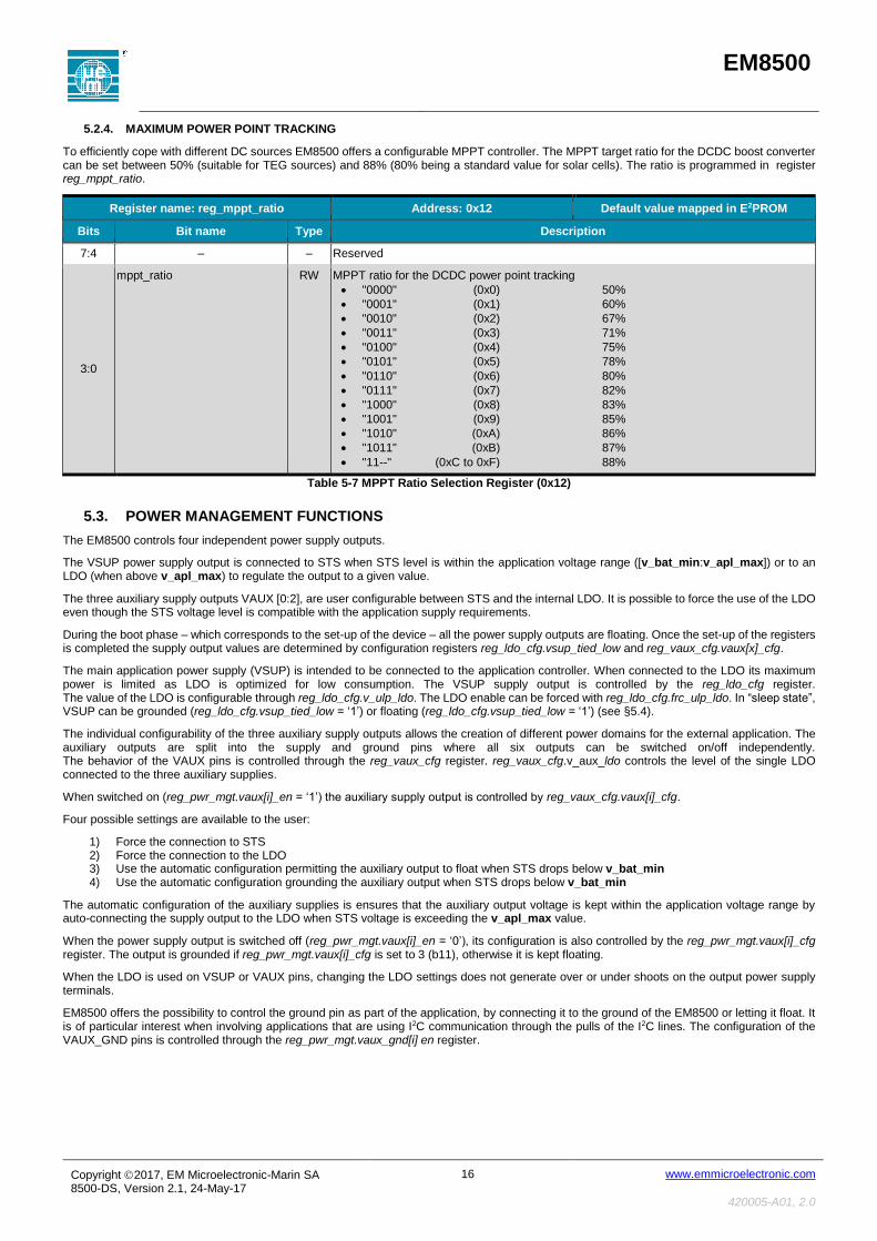
5.2.4. MAXIMUM POWER POINT TRACKING
To efficiently cope with different DC sources EM8500 offers a configurable MPPT controller. The MPPT target ratio for the DCDC boost converter can be set between 50% (suitable for TEG sources) and 88% (80% being a standard value for solar cells). The ratio is programmed in register reg_mppt_ratio.
Register name: reg_mppt_ratio Address: 0x12 Default value mapped in E2PROM
Bits Bit name Type Description
7:4 – – Reserved
3:0
mppt_ratio RW MPPT ratio for the DCDC power point tracking
"0000" (0x0) 50%
"0001" (0x1) 60%
"0010" (0x2) 67%
"0011" (0x3) 71%
"0100" (0x4) 75%
"0101" (0x5) 78%
"0110" (0x6) 80%
"0111" (0x7) 82%
"1000" (0x8) 83%
"1001" (0x9) 85%
"1010" (0xA) 86%
"1011" (0xB) 87%
"11--" (0xC to 0xF) 88%
Table 5-7 MPPT Ratio Selection Register (0x12)
5.3. POWER MANAGEMENT FUNCTIONS
The EM8500 controls four independent power supply outputs.
The VSUP power supply output is connected to STS when STS level is within the application voltage range ([v_bat_min:v_apl_max]) or to an LDO (when above v_apl_max) to regulate the output to a given value.
The three auxiliary supply outputs VAUX [0:2], are user configurable between STS and the internal LDO. It is possible to force the use of the LDO even though the STS voltage level is compatible with the application supply requirements.
During the boot phase – which corresponds to the set-up of the device – all the power supply outputs are floating. Once the set-up of the registers is completed the supply output values are determined by configuration registers reg_ldo_cfg.vsup_tied_low and reg_vaux_cfg.vaux[x]_cfg.
The main application power supply (VSUP) is intended to be connected to the application controller. When connected to the LDO its maximum power is limited as LDO is optimized for low consumption. The VSUP supply output is controlled by the reg_ldo_cfg register. The value of the LDO is configurable through reg_ldo_cfg.v_ulp_ldo. The LDO enable can be forced with reg_ldo_cfg.frc_ulp_ldo. In “sleep state”, VSUP can be grounded (reg_ldo_cfg.vsup_tied_low = ‘1’) or floating (reg_ldo_cfg.vsup_tied_low = ‘1’) (see §5.4).
The individual configurability of the three auxiliary supply outputs allows the creation of different power domains for the external application. The auxiliary outputs are split into the supply and ground pins where all six outputs can be switched on/off independently. The behavior of the VAUX pins is controlled through the reg_vaux_cfg register. reg_vaux_cfg.v_aux_ldo controls the level of the single LDO connected to the three auxiliary supplies.
When switched on (reg_pwr_mgt.vaux[i]_en = ‘1’) the auxiliary supply output is controlled by reg_vaux_cfg.vaux[i]_cfg.
Four possible settings are available to the user:
1) Force the connection to STS 2) Force the connection to the LDO 3) Use the automatic configuration permitting the auxiliary output to float when STS drops below v_bat_min 4) Use the automatic configuration grounding the auxiliary output when STS drops below v_bat_min
The automatic configuration of the auxiliary supplies is ensures that the auxiliary output voltage is kept within the application voltage range by auto-connecting the supply output to the LDO when STS voltage is exceeding the v_apl_max value.
When the power supply output is switched off (reg_pwr_mgt.vaux[i]_en = ‘0’), its configuration is also controlled by the reg_pwr_mgt.vaux[i]_cfg register. The output is grounded if reg_pwr_mgt.vaux[i]_cfg is set to 3 (b11), otherwise it is kept floating.
When the LDO is used on VSUP or VAUX pins, changing the LDO settings does not generate over or under shoots on the output power supply terminals.
EM8500 offers the possibility to control the ground pin as part of the application, by connecting it to the ground of the EM8500 or letting it float. It is of particular interest when involving applications that are using I2C communication through the pulls of the I2C lines. The configuration of the VAUX_GND pins is controlled through the reg_pwr_mgt.vaux_gnd[i] en register.
EM8500
Copyright 2017, EM Microelectronic-Marin SA 8500-DS, Version 2.1, 24-May-17
17 www.emmicroelectronic.com
420005-A01, 2.0
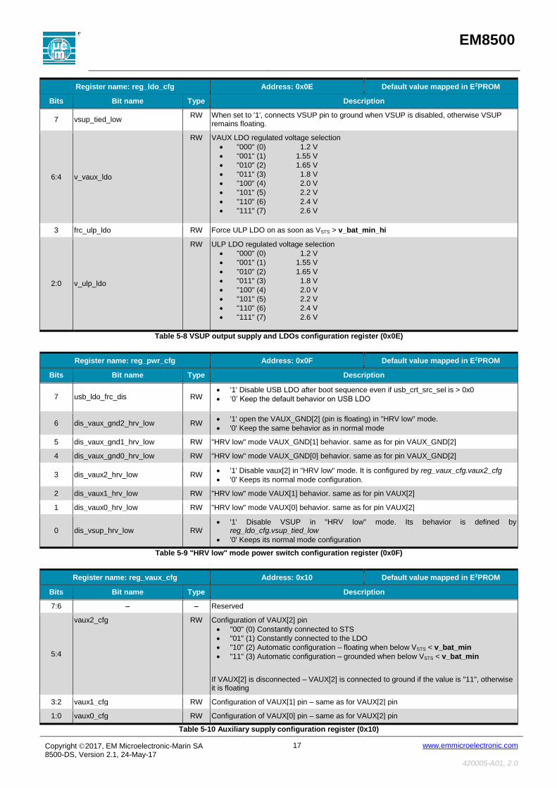
Register name: reg_ldo_cfg Address: 0x0E Default value mapped in E2PROM
Bits Bit name Type Description
7 vsup_tied_low RW When set to '1', connects VSUP pin to ground when VSUP is disabled, otherwise VSUP
remains floating.
6:4 v_vaux_ldo
RW VAUX LDO regulated voltage selection
"000" (0) 1.2 V
"001" (1) 1.55 V
"010" (2) 1.65 V
"011" (3) 1.8 V
"100" (4) 2.0 V
"101" (5) 2.2 V
"110" (6) 2.4 V
"111" (7) 2.6 V
3 frc_ulp_ldo RW Force ULP LDO on as soon as VSTS > v_bat_min_hi
2:0 v_ulp_ldo
RW ULP LDO regulated voltage selection
"000" (0) 1.2 V
"001" (1) 1.55 V
"010" (2) 1.65 V
"011" (3) 1.8 V
"100" (4) 2.0 V
"101" (5) 2.2 V
"110" (6) 2.4 V
"111" (7) 2.6 V
Table 5-8 VSUP output supply and LDOs configuration register (0x0E)
Register name: reg_pwr_cfg Address: 0x0F Default value mapped in E2PROM
Bits Bit name Type Description
7 usb_ldo_frc_dis RW '1' Disable USB LDO after boot sequence even if usb_crt_src_sel is > 0x0
‘0’ Keep the default behavior on USB LDO
6 dis_vaux_gnd2_hrv_low RW '1' open the VAUX_GND[2] (pin is floating) in "HRV low" mode.
'0' Keep the same behavior as in normal mode
5 dis_vaux_gnd1_hrv_low RW "HRV low" mode VAUX_GND[1] behavior. same as for pin VAUX_GND[2]
4 dis_vaux_gnd0_hrv_low RW "HRV low" mode VAUX_GND[0] behavior. same as for pin VAUX_GND[2]
3 dis_vaux2_hrv_low RW '1' Disable vaux[2] in "HRV low" mode. It is configured by reg_vaux_cfg.vaux2_cfg
'0' Keeps its normal mode configuration.
2 dis_vaux1_hrv_low RW "HRV low" mode VAUX[1] behavior. same as for pin VAUX[2]
1 dis_vaux0_hrv_low RW "HRV low" mode VAUX[0] behavior. same as for pin VAUX[2]
0 dis_vsup_hrv_low RW '1' Disable VSUP in "HRV low" mode. Its behavior is defined by
reg_ldo_cfg.vsup_tied_low
'0' Keeps its normal mode configuration
Table 5-9 "HRV low" mode power switch configuration register (0x0F)
Register name: reg_vaux_cfg Address: 0x10 Default value mapped in E2PROM
Bits Bit name Type Description
7:6 – – Reserved
5:4
vaux2_cfg RW Configuration of VAUX[2] pin
"00" (0) Constantly connected to STS
"01" (1) Constantly connected to the LDO
"10" (2) Automatic configuration – floating when below VSTS < v_bat_min
"11" (3) Automatic configuration – grounded when below VSTS < v_bat_min
If VAUX[2] is disconnected – VAUX[2] is connected to ground if the value is "11", otherwise it is floating
3:2 vaux1_cfg RW Configuration of VAUX[1] pin – same as for VAUX[2] pin
1:0 vaux0_cfg RW Configuration of VAUX[0] pin – same as for VAUX[2] pin
Table 5-10 Auxiliary supply configuration register (0x10)

EM8500
Copyright 2017, EM Microelectronic-Marin SA 8500-DS, Version 2.1, 24-May-17
18 www.emmicroelectronic.com
420005-A01, 2.0
Register name: reg_vaux_gnd_cfg Address: 0x11 Default value mapped in E2PROM
Bits Bit name Type Description
7:3 – – Reserved
2 vaux_gnd2_cfg RW '1' Auto disconnect when VSTS not within [v_bat_min.. v_apl_max]
'0' Fully manual connection
1 vaux_gnd1_cfg RW Configuration of VAUX_GND[1] pin – same as for VAUX_GND [2] pin
0 vaux_gnd0_cfg RW Configuration of VAUX_GND[0] pin – same as for VAUX_GND[2] pin
Table 5-11 Auxiliary ground pins configuration register (0x11)
Register name: reg_pwr_mgt Address: 0x19 Value at start-up mapped in E2PROM
Bits Bit name Type Description
7 frc_prim_dcdc_dis RW '1' Force the DCDC off
'0' Keep the automatic mode of the DCDC
6 vaux_gnd2_en RW Enable the VAUX_GND[2] connection (see reg_vaux_gnd_cfg.vaux_gnd2_cfg) when VSTS > v_bat_min_hi
5 vaux_gnd1_en RW Enable the VAUX_GND[1] connection (see reg_vaux_gnd_cfg.vaux_gnd0_cfg) when VSTS > v_bat_min_hi
4 vaux_gnd0_en RW Enable the VAUX_GND[0] connection (see reg_vaux_gnd_cfg.vaux_gnd0_cfg) when VSTS > v_bat_min_hi
3 vaux2_en RW Enable the VAUX[2] connection (see reg_vauxcfg.vaux2_cfg) when VSTS > v_bat_min_hi
2 vaux1_en RW Enable the VAUX[1] connection (see reg_vauxcfg.vaux1_cfg) when VSTS > v_bat_min_hi
1 vaux0_en RW Enable the VAUX[0] connection (see reg_vauxcfg.vaux0_cfg) when VSTS > v_bat_min_hi
0 sleep_vsup RW Enable the VSUP "sleep state" – disconnects VSUP for t_sleep_vsup interval
Table 5-12 Power switch enable register (0x19)
5.4. PRIMARY CELL CONFIGURATION
The EM8500 supports supplying an application through a combination of a primary cell and a harvesting element by setting reg_lts_cfg.prim_cell to ‘1’.
In this case the application is mainly supplied by STS. LTS is automatically connected to STS as soon as the harvesting element is not providing enough energy to supply the application. LTS is disconnected from STS as soon as the harvester provides enough energy to the system again.
LTS and STS are connected automatically when HRV_LOW is asserted, or if after a measurement of VSTS below v_bat_min_hi_dis, a successive measurement (1 ms later) on STS confirms that the level is still below v_bat_min_hi_dis. The connection remains for two periods of HRV measurements.
If the battery level is below v_bat_min_lo STS and LTS are kept disconnected to avoid damaging the battery cell.
The checks on the harvester and STS are done with the same frequencies as shown in §5.2.1.
It is possible to force the connection between STS and LTS, preventing the use of the DCDC converter to harvest energy from the harvester cell – reg_lts_cfg.prim_cell_connect = ‘1’. This is particularly useful to perform high energy tasks.
When the device is in LTS protect mode (reg.status.lts_protect = ‘1’) forcing the primary cell connection has no effect. The system continues to be supplied by the harvester. Forcing a connection leads to the collapse of the supply as the battery is too low.
By permanently connecting STS and LTS it is also possible to use only a primary cell (without harvester) and taking advantage of the EM8500 power management features to control the 4 power supply domains and their automated nodes.
Register name: reg_lts_cfg Address: 0x06 Default value mapped in E2PROM
Bits Bit name Type Description
7:3 – – Reserved
2 prim_cell_connect RW '1' Connect LTS and STS if reg_lts_cfg.prim_cell = ‘1’.
‘0’ Normal mode on STS
1 prim_cell RW '1' Sets the device in primary cell mode. The DCDC never charges LTS
‘0’ Sets the device in secondary cell mode (LTS is rechargeable)
0 no_bat_protect RW '1' Disables the battery protection feature. (reg.status.lts_protect = ‘0’)
‘0’ Enables the battery protection feature.
Table 5-13 LTS configuration register (0x06)
EM8500
Copyright 2017, EM Microelectronic-Marin SA 8500-DS, Version 2.1, 24-May-17
19 www.emmicroelectronic.com
420005-A01, 2.0
When the primary cell mode is selected the lux-meter function can only be used when both LTS and STS are forced to be connected together – reg_lts_cfg.prim_cell_connect = ‘1’.
5.5. SLEEP MODE AND WAKE-UP FUNCTIONS
In addition to the direct control of the power supply outputs the EM8500 supports stopping supplying the application (switching off VSUP) for a given time interval to allow very low consumption modes. When enabled, the auxiliary supplies are kept in the same state as before entering in the “sleep state”. The “sleep state” is not a functional mode of the power management unit, as the device is still working according to the configuration parameters set and is only acting on the state of the VSUP supply output.
The “sleep state” can also be interrupted (VSUP is connected again on STS or on the LDO according to the settings of the VSUP power switch see Table 5-8) by setting the WAKE_UP pin to a level above Vih_wk.
During “sleep state” the serial interface is disabled.
To avoid false wake-up detection, a debouncing logic is connected to the WAKE_UP pin. The debouncer function is enabled by default (factory default value on E2PROM), and can be disabled by setting the reg_ext_cfg. wake_up_deb_en to ‘0’. The wake-up is sensitive to the edge configured in reg_ext_cfg.wake_up_edge_cfg. It is not permitted to set reg_ext_cfg.wake_up_edge_cfg = “00”.
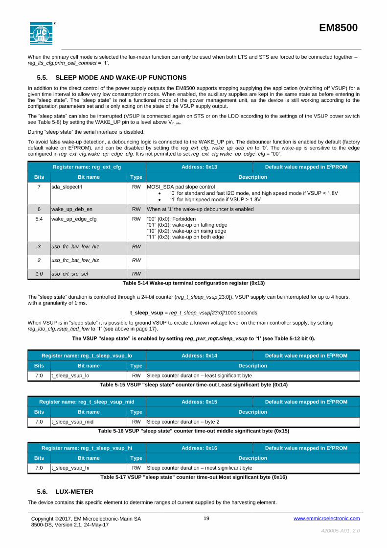
Register name: reg_ext_cfg Address: 0x13 Default value mapped in E2PROM
Bits Bit name Type Description
7 sda_slopectrl RW MOSI_SDA pad slope control
‘0’ for standard and fast I2C mode, and high speed mode if VSUP < 1.8V
‘1’ for high speed mode if VSUP > 1.8V
6 wake_up_deb_en RW When at '1' the wake-up debouncer is enabled
5:4 wake_up_edge_cfg RW “00” (0x0): Forbidden “01” (0x1): wake-up on falling edge “10” (0x2): wake-up on rising edge “11” (0x3): wake-up on both edge
3 usb_frc_hrv_low_hiz RW
2 usb_frc_bat_low_hiz RW
1:0 usb_crt_src_sel RW
Table 5-14 Wake-up terminal configuration register (0x13)
The “sleep state” duration is controlled through a 24-bit counter (reg_t_sleep_vsup[23:0]). VSUP supply can be interrupted for up to 4 hours, with a granularity of 1 ms.
t_sleep_vsup = reg_t_sleep_vsup[23:0]/1000 seconds
When VSUP is in “sleep state” it is possible to ground VSUP to create a known voltage level on the main controller supply, by setting reg_ldo_cfg.vsup_tied_low to ‘1’ (see above in page 17).
The VSUP “sleep state” is enabled by setting reg_pwr_mgt.sleep_vsup to ‘1’ (see Table 5-12 bit 0).
Register name: reg_t_sleep_vsup_lo Address: 0x14 Default value mapped in E2PROM
Bits Bit name Type Description
7:0 t_sleep_vsup_lo RW Sleep counter duration – least significant byte
Table 5-15 VSUP "sleep state" counter time-out Least significant byte (0x14)
Register name: reg_t_sleep_vsup_mid Address: 0x15 Default value mapped in E2PROM
Bits Bit name Type Description
7:0 t_sleep_vsup_mid RW Sleep counter duration – byte 2
Table 5-16 VSUP "sleep state" counter time-out middle significant byte (0x15)
Register name: reg_t_sleep_vsup_hi Address: 0x16 Default value mapped in E2PROM
Bits Bit name Type Description
7:0 t_sleep_vsup_hi RW Sleep counter duration – most significant byte
Table 5-17 VSUP "sleep state" counter time-out Most significant byte (0x16)
5.6. LUX-METER
The device contains this specific element to determine ranges of current supplied by the harvesting element.

EM8500
Copyright 2017, EM Microelectronic-Marin SA 8500-DS, Version 2.1, 24-May-17
20 www.emmicroelectronic.com
420005-A01, 2.0
The lux-meter is able to run in three modes:
Fully automatic mode
Automatic range selection
Fully manual mode
In fully automatic mode (selected by writing ‘1’ in reg_lux_meter_cfg.lux_meter_auto_meas) the device determines the value range for the current flowing in from the harvesting element. The result is available in the reg_lux_meter_result.lux_meter_result register field. The reg_lux_meter_result.lux_meter_busy bit indicates that the measurement is still ongoing and that the result is not available yet.
In automatic range selection mode (selected by writing ‘1’ in reg_lux_meter_cfg.lux_meter_auto_rng) the EM8500 automatically determines the optimal range, and measures the voltage at VDD_HRV for maximum precision. The reg_lux_meter_result.lux_meter_busy bit indicates that the range search is complete. In this mode lux-meter continues to operate until user disabled by writing ‘0’ into the reg_lux_meter_cfg.lux_meter_auto_rng.
The full manual mode allows the user to select the range. The mode is selected by writing on the bit reg_lux_meter_cfg.lux_meter_manu – ‘1’ to activate the mode, and ‘0’ to deactivate it. The selection of the range is done through the reg_lux_meter_cfg.lux_meter_rng field.
In case a lux-meter action is requested with LTS and STS disconnected, VLTS < v_bat_min_lo or – in primary cell mode – when reg_lts_cfg.prim_cell_connect = ‘0’ the action is disregarded and the result – in automatic mode – is invalid.
Register name: reg_lux_meter_cfg Address: 0x1C
Bits Bit name Type Reset Description
7 – – 0 Reserved
6 lux_auto_meas OS 0 Start the automatic lux-meter measurement. The lux-meter is disabled automatically when the measure is finished
5 lux_auto_rng RW 0 Enable the lux-meter, and search for the best range. It remains enabled
4 lux_manu RW 0 Enable the lux-meter in manual mode (range forced by reg_lux_meter_cfg.lux_lvl)
3:0 lux_lvl RW 0x0
Target current level to be detected
"0000" (0x0) 1 µA
"0001" (0x1) 2 µA
"0010" (0x2) 4 µA
"0011" (0x3) 8 µA
"0100" (0x4) 15 µA
"0101" (0x5) 30 µA
"0110" (0x6) 60 µA
"0111" (0x7) 120 µA
"1000" (0x8) 0.25 mA
"1001" (0x9) 0.5 mA
"1010" (0xA) 1 mA
"1011" (0xB) 1.8 mA
"1100" (0xC) 3.2 mA
"1101" (0xD) 6 mA
"1110" (0xE) 11 mA
"1111" (0xF) 17 mA
Table 5-18 Lux Meter Configuration Register (0x1C)

EM8500
Copyright 2017, EM Microelectronic-Marin SA 8500-DS, Version 2.1, 24-May-17
21 www.emmicroelectronic.com
420005-A01, 2.0
Register name: reg_lux_meter_result Address: 0x1D
Bits Bit name Type Reset Description
7:5 – – '000' Reserved
4 lux_meter_busy RO 0 Indicates that the lux-meter is still searching for best range
3:0 lux_meter_result RO 0x0
Lux-meter range status (result in automatic measurement mode)
"0000" (0x0) below 2 µA
"0001" (0x1) from 2 µA to 4 µA
"0010" (0x2) from 4 µA to 8 µA
"0011" (0x3) from 8 µA to 15 µA
"0100" (0x4) from 15 µA to 30 µA
"0101" (0x5) from 30 µA to 60 µA
"0110" (0x6) from 60 µA to 120 µA
"0111" (0x7) from 120 µA to 0.25 mA
"1000" (0x8) from 0.25 mA to 0.5 mA
"1001" (0x9) from 0.5 mA to 1 mA
"1010" (0xA) from 1 mA to 1.8 mA
"1011" (0xB) from 1.8 mA to 3.2 mA
"1100" (0xC) from 3.2 mA to 6 mA
"1101" (0xD) from 6 mA to 11 mA
"1110" (0xE) from 11 mA to 17 mA
"1111" (0xF) above 17 mA
Table 5-19 Lux-meter Result Register (0x1D)
5.7. USB CHARGING
The EM8500 is equipped with a USB power line input to supply the device and to charge has the energy bank elements.
When a voltage above Vusb_min is detected, a regulator between VDD_USB and VDD_STS is enabled. The regulated voltage is VUSB_REG. In addition to the regulator, a current source is activated between VDD_USB and VDD_LTS. This function is controlled by the reg_ext_cfg register. Four user selected level of charge current delivered to LTS are available (reg_ext_cfg.usb_crt_src_sel).
When VDD_USB is connected, pins HRV_LOW and BAT_LOW can be brought into HiZ state.
Register name: reg_ext_cfg Address: 0x13 Default value mapped in E2PROM
Bits Bit name Type Description
7 sda_slopectrl RW
6 wake_up_deb_en RW
5:4 wake_up_edge_cfg RW
3 usb_frc_hrv_low_hiz RW ‘1’ force HRV_LOW in Hi-Z state if usb_on = '1'
‘0’ HRV_LOW pin standard configuration
2 usb_frc_bat_low_hiz RW ‘1’ force BAT_LOW in Hi-Z state if usb_on = '1'
‘0’ BAT_LOW pin standard configuration
1:0 usb_crt_src_sel RW USB power current source selection
"00" (0x0) 0 mA (do not charge)
"01" (0x1) 5 mA
"10" (0x2) 10 mA
"11" (0x3) 20 mA
Table 5-20 USB Configuration Register (0x13)
Warning: When VDD_LTS is to be disconnected from its load, the USB current injected into LTS must be set to 0 mA, otherwise the device could be damaged.
5.8. MISCELLANEOUS FUNCTIONS
This chapter describes additional control functions related to the regulation loop.
5.8.1. SOFT RESET FUNCTION
The soft reset function restarts the EM8500 from its boot sequence. The behavior of the EM8500 is the same as in a normal boot sequence. A soft reset is generated by setting the register reg_soft_res_word to 0xAB. This register is enabled only if reg_protect_key is set to 0xE2. If the value of the reg_protect_key is different from 0xE2, the register reg_soft_res_word is set to 0x00.
The reg_protect_key register is reset by the soft reset. Creating a new soft sequence requires preloading the reg_protect_key again.

EM8500
Copyright 2017, EM Microelectronic-Marin SA 8500-DS, Version 2.1, 24-May-17
22 www.emmicroelectronic.com
420005-A01, 2.0
Register name: reg_soft_res_word Address: 0x1A
Bits Bit name Type Reset Description
7:0 soft_res_word RW 0x00 Force reset when set at 0xAB
Table 5-21 Soft reset register (0x1A)
Register name: reg_protect_key Address: 0x1B
Bits Bit name Type Reset Description
7:0 protect_key RW 0x00 Allow writing on reg_soft_res_word register when set at 0xE2 Allow writing on protected registers when set at 0x4B Allow writing on E2PROM when set at 0xA5
Table 5-22 Protected registers key (0x1B)
5.8.2. REGISTER PROTECTION
The EM8500 functionality is determined by the content of the configuration registers (like the supervising levels or periods). The registers are always accessible in read mode. Some registers are write protected against unwanted write operations.
The registers ranging is address space from 0x00 to 0x18 are write protected. Writing into these registers is enabled after setting reg_protect_key to 0x4B.
Note: The reg_protect_key is reset at the end of the communication transaction (see §6 on page 22). It is necessary to set it on the same communication transaction – on SPI keeping CS to ‘1’ or on I2C before putting a I2C stop.
Write access to the on-chip E2PROM is controlled by the same mechanism. Prior to a write operation into the E2PROM reg_protect_key must be set to 0xA5.
5.8.3. LTS PROTECTION DISABLE
By default the EM8500’s monitors voltage levels, namely lower voltage limit, to prevent damage to the LTS energy storage element.
This protection can be disabled by setting register reg_lts_cfg.no_bat_protect leaving the system connected to LTS even when the voltage level drops below v_bat_min. Disabling protection might be suitable for systems using super-caps or solid-state battery storage elements.
When LTS protection is active the EM8500 tries to start-up from LTS only once, if after booting it still detects that VLTS < v_bat_min it enables the protection and never try to restart from LTS. The system will then re-start as from a standard cold-start.
5.8.4. DCDC OFF FORCING
It is possible to stop the regulation loop by explicitly forcing the DCDC to stop its pumping operation. To stop the DCDC it is necessary to set the bit reg_pwr_mgt.frc_prim_dcdc_dis to ‘1’ (see Table 5-12). De-asserting this bit (write it to ‘0’) will re-enable the DCDC to its normal operation.
6. SERIAL INTERFACE
The EM8500 offers SPI and I2C serial interfaces selected by the CS pin.(see §6.2.1).
The configuration/function of the EM8500 is updated only after the end of a communication transaction. An SPI transaction is defined by all the bytes sent and received when the pad CS is kept to ‘1’. An I2C transaction is defined by all the data sent or received between a start and a stop I2C patterns.
Data synchronization between the communication interface and the internal part of the device is done at the end of a supervising loop. New information is active two milliseconds after the end of the transaction. All write transactions sent before the end of this synchronization interval are ignored. It is recommended to perform the device configuration in one transaction. Read transactions are allowed at any time.
6.1. I2C INTERFACE
The I2C slave interface is compatible with Philips I2C Specification version 2.1 (see specific timings on electrical specifications chapter). All modes (standard, fast, high speed) are supported. MOSI_SDA and SCL pins are not strictly open-drain (they represent diodes to VSUP).
The 7-bit device address is defined in the E2PROM (at address 0x58). This address is copied at boot into the reg_spi_i2c_cfg.ic2_addr register field.
The I2C bus uses the 2 wires SCL (Serial Clock) and MOSI_SDA. CS has to be connected to VSS. MOSI_SDA is bi-directional with open drain to VSS: it must be externally connected to VSUP via a pull up resistor.
The I2C interface supports single and multiple read and write transactions.
In the following figures, “S” indicates the I2C transaction start, “P” indicates the I2C transaction stop.
The multi-read and multi write transactions are described in the following figures.

EM8500
Copyright 2017, EM Microelectronic-Marin SA 8500-DS, Version 2.1, 24-May-17
23 www.emmicroelectronic.com
420005-A01, 2.0
SCL
S Pi2c addressWrite
Register address (n) Register value to be written @ nAddress/data couple to be
written
MOSI_SDA
ACKS ACKS ACKS
Figure 6-1: I2C write (multiple transactions)
To access registers in read mode, first address should first be send in write mode. Then a stop and a start conditions must be generated and data bytes are transferred with automatic address increment:
SCL
MOSI_SDA
SCL
MOSI_SDA
S Pi2c addressRead
Register read @ n Register read @ n+1, n+2, ...
ACKS ACKM NOACKM
i2c addressWrite
Register address (n)
ACKS ACKS
Figure 6-2: I2C read (multiple transactions)
In the case of a read transaction, it is possible to avoid stopping and starting again a new transaction by following the register address with a repeated start.
6.2. SPI INTERFACE
The SPI interface is a standard Serial to Peripheral Interface. It is compatible with two of the four standard transmission modes. The automatic selection between the two modes ([CPOL=’0’ and CPHA=’0’] and [CPOL=’1’ and CPHA=’1’]) is determined by the value of SCL after the CS rising edge.
The SPI interface can be used in 4-wire or 3-wire. The 3-wire is selected by setting the register reg_spi_i2c_cfg.spi_3w_en to '1’. The pin MOSI is used as a data pin in 3-wire mode.
The SPI interface is a byte-oriented transmission interface. The first byte sent is contains the address of the register and access type of the transmission – on the first transmitted bit (reads register – ‘1’ – or writes register – ‘0’). The following bytes contain register values. On read access the address read is incremented for each additional byte until the address 0x7F. When reaching this address, the devices internal address counter wraps to 0x00 and starts to read again from this address.
In case of a write transaction the protocol is based on an interleaved scheme of address and data. The first byte contains a 7-bit address and the write command (First sent bit of the first byte equal to ‘0’). The second byte contains data to be written to this address.
It is important to note that it is possible to send a set of write commands, followed by a multi read transaction within the same SPI transaction. Once in read mode, write accesses are not possible anymore in the same SPI transaction.
The following example shows a write of some registers followed by a check of the data.
0x00 0x05 0x01 0x03 0x06 0x02 0x80 0x00 0x00 0x00 0x00 Set hrv_period to 1/8 Hz Set hrv_meas to 128ms Set the system in primary cell mode Read registers 0x00 to 0x03
CS
SCL
MOSI_SDA R_Wn AD6 AD5 AD4 AD3 AD2 AD1 AD0 DI7 DI6 DI5 DI4 DI3 DI2 DI1 DI0
MISO ST7 ST6 ST5 ST4 ST3 ST2 ST1 ST0 DO7 DO6 DO5 DO4 DO3 DO2 DO1 DO0
Figure 6-3 SPI transaction scheme CPOL=1, CPHA=1

EM8500
Copyright 2017, EM Microelectronic-Marin SA 8500-DS, Version 2.1, 24-May-17
24 www.emmicroelectronic.com
420005-A01, 2.0
CS
SCL
MOSI_SDA R_Wn AD6 AD5 AD4 AD3 AD2 AD1 AD0 DI7 DI6 DI5 DI4 DI3 DI2 DI1 DI0
MISO ST6 ST5 ST4 ST3 ST2 ST1 ST0 DO7 DO6 DO5 DO4 DO3 DO2 DO1 DO0ST7
Figure 6-4 SPI transaction scheme CPOL=0, CPHA=0
CS
SCL
MISO
MISO
address "x", access type (read) and status byte
Mu
tli w
rite
Mu
tli r
ead
MOSI_SDA
MOSI_SDA
status
data to be written in 'x', output at '0'
address "x", access type (write) and status byte
address data to be written address data to be written
Next address/data couple other address/data couple
address "n"
status data @ n data @ n+1 data @ n+2 data @ x
Figure 6-5 Multi register access transaction
Along with the address information the SPI interface sends the status register (reg_status – address 0x22) as the first response byte. In the case of the 3-wire mode the protocol is identical to the I2C interface, and doesn’t allow having the status byte when sending the address to the device.
Interface signals are the following:
CS chip select, active high SCL clock MOSI_SDA data input; data input/output in 3-wire mode MISO data output; Hi-Z level in 3-wire mode
6.2.1. INTERFACE SELECTION
The interface selection process is done through the use of the CS pin.
At reset (at the end of the boot sequence) the default interface selection is I2C. The SPI selection is done by asserting the CS pin. After CS assertion the SPI interface is selected until the device is shut-down (VSTS below Vcs_lo).
If the CS pin is continuously asserted (through a hard connection to VSUP) the SPI interface is permanently selected. I2C is not available in this case.
Register name: reg_spi_i2c_cfg Address: 0x18 Default value mapped in E2PROM
Bits Bit name Type Description
7 spi_3w_en RW Set the SPI in its 3 wire mode (shared MOSI/MISO)
6:0 i2c_addr RW i2c address
Table 6-1 SPI/I2C configuration register (0x18)
6.3. E2PROM
6.3.1. ACCESSING THE E2PROM
The on-chip E2PROM contains the default working parameters of the device. The E2PROM address space is mapped into the EM8500 register map from address 0x40 (E2PROM address 0) to 0x7F ((E2PROM address 63). Some addresses are reserved (0x76 to 0x7F) and are accessible in read-only mode by the user; some contains the defaults values – as described on §8. All other addresses can be freely used.
The user can write on the E2PROM at any time. Note that no protection is built in to prevent incomplete write transaction caused by a lack of energy (STS too low). The user must ensure that the EM8500 is able to properly finish a write transaction.
Read and write accesses are performed through the serial interface. In difference to standard registers (addresses 0x00 to 0x3F), an E2PROM access requires a dead time. A read access needs a dead time between read address and the data. A write access requires a dead time after having sent the write data.

EM8500
Copyright 2017, EM Microelectronic-Marin SA 8500-DS, Version 2.1, 24-May-17
25 www.emmicroelectronic.com
420005-A01, 2.0
CS
SCL
MOSI_SDA
MISO
Tee_rd
Figure 6-6 SPI transaction for reading the E2PROM (CPOL=1)
CS
MOSI_SDA
MISO
Tee_rd
SCL
Figure 6-7 SPI transaction for reading the E2PROM (CPOL=0)
CS
SCL
MOSI_SDA
MISO status data @ n status data @ m
address "n" address "m"
Thd_rd Tee_rdTee_rd
Table 6-2 SPI multiple E2PROM read transactions
CS
SCL
MOSI_SDA
MISO
Tee_wr
0xA50x1B E2PROM address data
status
Tee_wr
0xA50x1B E2PROM address data
status
Figure 6-8 Two consecutive single E2PROM write SPI transactions
CS
SCL
MOSI_SDA
MISO
Tee_wr
0xA50x1B E2PROM address data
status
E2PROM address data
Tee_wr
Figure 6-9 SPI multi-byte transaction for writing the E2PROM
When the I2C serial interface is used only single action per transaction is allowed when accessing the E2PROM. As for an SPI transaction a dead time are necessary. Prior to a write transaction into the E2PROM it is necessary to set the reg_protection_key register to 0xA5.
For a write transaction, no other I2C transaction into the E2PROM address area is allowed for Twr_ee after the end of the write transaction. A transaction inside this time window is ignored by the device.
In the following diagram responses from EM8500 are shown in red, data from the I2C master in black.
The following abbreviations are used:
W Write transaction request
R Read transaction request
S Start an I2C transaction

EM8500
Copyright 2017, EM Microelectronic-Marin SA 8500-DS, Version 2.1, 24-May-17
26 www.emmicroelectronic.com
420005-A01, 2.0
P Stop an I2C transaction
A I2C Acknowledge
N I2C Non Acknowledge
SCL
MOSI_SDA I2C address WA
Tee_wr
S 0x1B A 0xA5 A reg address A reg data P I2C address WAS 0x1B A 0xA5 A reg address A reg data P
Tee_wr
Figure 6-10 I2C transaction for writing on the E2PROM
For a read transaction a dead-time (Trd_ee) has to be inserted in between the address setting transaction and the read action itself.
SCL
MOSI_SDA S I2C address W A Register address A P S I
2C address R A Read data N P
Tee_rd
Figure 6-11 I2C transaction for reading the E2PROM

EM8500
Copyright 2017, EM Microelectronic-Marin SA 8500-DS, Version 2.1, 24-May-17
27 www.emmicroelectronic.com
420005-A01, 2.0
7. TYPICAL CHARACTERISTICS
Figure 7-1 Charger Efficiency vs Input Voltage (IIN = 10µA)
Figure 7-2 Charger Efficiency vs Input Current (VIN = 1.5V)
Figure 7-3 Charger Efficiency vs Input Voltage (IIN = 100µA)
Figure 7-4 Charger Efficiency vs Input Current (VIN = 0.5V)
Figure 7-5 Charger Efficiency vs Input Voltage (IIN = 1mA)
Figure 7-6 Charger Efficiency vs Input Current (VIN = 0.2V)

EM8500
Copyright 2017, EM Microelectronic-Marin SA 8500-DS, Version 2.1, 24-May-17
28 www.emmicroelectronic.com
420005-A01, 2.0
8. REGISTER MAP
Index
0
t_h
rv_
peri
od
(2:0
)
t_h
rv_
me
as(2
:0)
t_sts
_p
eri
od
(2:0
)
t_lts_
pe
riod(2
:0)
v_
hrv
_m
in(5
:0)
hrv
_ch
eck_
lvl(3
:0)
no
_b
at_
pro
tect
v_
ba
t_m
ax_
hi(
5:0
)
v_
ba
t_m
ax_
lo(5
:0)
v_
ba
t_m
in_h
i_d
is(5
:0)
v_
ba
t_m
in_h
i_co
n(5
:0)
v_
ba
t_m
in_
lo(5
:0)
v_
ap
l_m
ax_h
i(5
:0)
v_
ap
l_m
ax_
lo(5
:0)
v_
ulp
_ld
o(2
:0)
dis
_vsu
p_
hrv
_lo
w
va
ux0
_cfg
(1:0
)
va
ux_
gn
d0_
cfg
mp
pt_
ratio
(3:0
)
usb
_crt
_src
_se
l(1
:0)
t_sle
ep
_vsu
p_
lo(7
:0)
t_sle
ep
_vsu
p_
mid
(7:0
)
t_sle
ep
_vsu
p_
hi(
7:0
)
t_lts_
hrv
_lo
w_p
eri
od(2
:0)
i2c_
ad
dr(
6:0
)
sle
ep
_vsu
p
No
te:
Ita
lic-u
nd
erl
ine
d r
eg
iste
rs a
re p
rote
cte
d a
ga
inst
accid
en
tal w
rite
actio
n. F
or
wri
tin
g t
hose
re
gis
ters
it
is r
equ
ire
d to
fir
st
wri
te r
eg
_p
rote
ct_
ke
y t
o 0
x4
B,
be
fore
wri
ting
in
to th
em
with
in t
he
sa
me
co
mm
un
ication t
ran
sa
ctio
n –
se
e §
5.8
.2
1
pri
m_
ce
ll
dis
_va
ux0
_hrv
_lo
w
va
ux_
gn
d1_
cfg
va
ux0
_e
n
2
pri
m_
ce
ll_con
ne
ct
dis
_va
ux1
_hrv
_lo
w
va
ux1
_cfg
(1:0
)
va
ux_
gn
d2_
cfg
usb
_fr
c_
ba
t_lo
w_
hiz
va
ux1
_e
n
3
- - - - -
frc_
ulp
_ld
o
dis
_va
ux2
_hrv
_lo
w
-
usb
_fr
c_
hrv
_lo
w_
hiz
-
va
ux2
_e
n
4
- - - - - -
v_
va
ux_
ldo
(2:0
)
dis
_vaux_gnd0
_hrv
_lo
w
va
ux2
_cfg
(1:0
)
- -
wake
_u
p_
edg
e_
cfg
(1:0
)
t_h
rv_
low
_pe
riod(2
:0)
va
ux_
gn
d0_
en
5
- - - - - -
dis
_vaux_gnd1
_hrv
_lo
w
- -
va
ux_
gn
d1_
en
6 - - - -
hrv
_ch
eck_
vld
- - - - - - - - -
dis
_vaux_gnd2
_hrv
_lo
w
- - -
wake
_u
p_
deb
_e
n
va
ux_
gn
d2_
en
7 - - - - - - - - - - - - - -
vsu
p_
tie
d_
low
usb
_ld
o_
frc_
dis
- - -
sd
a_
slo
pe
ctr
l
-
sp
i_3
w_e
n
frc_
pri
m_
dcd
c_
dis
Fa
cto
ry
Valu
e
0x0
6
0x0
6
0x0
2
0x0
5
0x0
1
0x0
4
0x0
0
0x2
A
0x2
9
0x1
E
0x1
E
0x1
D
0x2
5
0x2
1
0xC
F
0x7
E
0x1
5
0x0
1
0x0
6
0x6
5
0x9
9
0x3
A
0x0
0
0x6
7
0x7
7
0x0
0
Addre
ss
Dec
1
2
3
4
5
6
7
8
9
10
11
12
13
14
15
16
17
18
19
20
21
22
23
24
25
Hex
0x0
0
0x0
1
0x0
2
0x0
3
0x0
4
0x0
5
0x0
6
0x0
7
0x0
8
0x0
9
0x0
A
0x0
B
0x0
C
0x0
D
0x0
E
0x0
F
0x1
0
0x1
1
0x1
2
0x1
3
0x1
4
0x1
5
0x1
6
0x1
7
0x1
8
0x1
9
Regis
ter
Nam
e
reg
_t_
hrv
_p
eri
od
reg
_t_
hrv
_m
ea
s
reg
_t_
sts
_p
eri
od
reg
_t_
lts_p
eri
od
reg
_v_
hrv
_cfg
reg
_h
rv_
ch
eck_
lvl
reg
_lts_
cfg
reg
_v_
bat_
ma
x_
hi
reg
_v_
bat_
ma
x_
lo
reg
_v_
bat_
min
_h
i_d
is
reg
_v_
bat_
min
_h
i_co
n
reg
_v_
bat_
min
_lo
reg
_v_
ap
l_m
ax_
hi
reg
_v_
ap
l_m
ax_
lo
reg
_ld
o_
cfg
reg
_p
wr_
cfg
reg
_va
ux_
cfg
reg
_va
ux_g
nd
_cfg
reg
_m
pp
t_ra
tio
reg
_e
xt_
cfg
reg
_t_
sle
ep
_vsu
p_
lo
reg
_t_
sle
ep
_vsu
p_m
id
reg
_t_
sle
ep
_vsu
p_h
i
reg
_t_
hrv
_lo
w_
cfg
reg
_sp
i_i2
c_
cfg
reg
_p
wr_
mg
t
Table 8-1 Register summary with default value defined in E2PROM

EM8500
Copyright 2017, EM Microelectronic-Marin SA 8500-DS, Version 2.1, 24-May-17
29 www.emmicroelectronic.com
420005-A01, 2.0
Index
0
so
ft_
res_
word
(7:0
)
pro
tect_
ke
y(7
:0)
lux_
lvl(
3:0
)
lux_
me
ter_
resu
lt(3
:0)
lts_
pro
tect
sts
_b
at_
min
_lo
No
te:
Ita
lic-u
nd
erl
ine
d r
eg
iste
r (r
eg
_so
ft_re
s_w
ord
) is
pro
tecte
d a
ga
inst a
ccid
en
tal w
rite
actio
n.
For
wri
ting
it, it
is r
equ
ire
d to
fir
st
wri
te r
eg_
pro
tect_
ke
y t
o 0
xE
2,
be
fore
wri
ting in
to t
he
m w
ith
in t
he
sam
e c
om
mu
nic
ation
tra
nsa
ctio
n –
se
e
§5
.8.2
1
usb
_o
n
sts
_b
at_
min
_h
i
2
sw
_lts_
sts
sts
_a
pl_
ma
x_
lo
3
sw
_vd
cd
c_
lts_
nsts
sts
_a
pl_
ma
x_h
i
4
lux_
ma
nu
lux_
me
ter_
bu
sy
ba
t_lo
w
sts
_b
at_
ma
x_
lo
5
lux_
au
to_
rng
-
hrv
_lo
w
sts
_b
at_
ma
x_
hi
6
lux_
au
to_
me
as
-
hrv
_lu
x_
bu
sy
lts_
ba
t_m
in_
lo
7
- -
ee
pro
m_
da
ta_
bu
sy
lts_
ba
t_m
in_h
i
Reset
Valu
e
0x0
0
0x0
0
0x0
0
0x0
0
0x0
0
0x0
0
Addre
ss
Dec
26
27
28
29
34
35
Hex
0x1
A
0x1
B
0x1
C
0x1
D
0x2
2
0x2
3
Regis
ter
Nam
e
reg
_so
ft_
res_
word
reg
_p
rote
ct_
ke
y
reg
_lu
x_m
ete
r_cfg
reg
_lu
x_m
ete
r_re
su
lt
reg
_sta
tus
reg
_vld
_sta
tus
Table 8-2 Register summary – No E2PROM default values

EM8500
Copyright 2017, EM Microelectronic-Marin SA 8500-DS, Version 2.1, 24-May-17
30 www.emmicroelectronic.com
420005-A01, 2.0
Ind
ex
0
t_h
rv_
peri
od
(2:0
)
t_h
rv_
me
as(2
:0)
t_sts
_p
eri
od
(2:0
)
t_lts_
pe
riod(2
:0)
v_
hrv
_m
in(5
:0)
hrv
_ch
eck_
lvl(3
:0)
no
_b
at_
pro
tect
v_
ba
t_m
ax_
hi(
5:0
)
v_
ba
t_m
ax_
lo(5
:0)
v_
ba
t_m
in_h
i_d
is(5
:0)
v_
ba
t_m
in_h
i_co
n(5
:0)
v_
ba
t_m
in_
lo(5
:0)
v_
ap
l_m
ax_h
i(5
:0)
v_
ap
l_m
ax_
lo(5
:0)
v_
ulp
_ld
o(2
:0)
dis
_vsup_hrv
_lo
w
va
ux0
_cfg
(1:0
)
va
ux_
gn
d0_
cfg
mp
pt_
ratio
(3:0
)
usb
_crt
_src
_se
l(1
:0)
t_sle
ep
_vsu
p_
lo(7
:0)
t_sle
ep
_vsu
p_
mid
(7:0
)
t_sle
ep
_vsu
p_
hi(
7:0
)
t_lts_
hrv
_lo
w_p
eri
od(2
:0)
i2c_
ad
dr(
6:0
)
sle
ep
_vsu
p
No
te:
All
E2P
RO
M is p
rote
cte
d a
ga
inst a
ccid
en
tal w
rite
action
. F
or
wri
ting in
to t
he E
2P
RO
M it
is r
eq
uir
ed
to
fir
st
wri
te in
to r
eg_
pro
tect_
ke
y th
e v
alu
e 0
xA
5,
be
fore
wri
ting
in
to it
with
in t
he s
am
e c
om
mu
nic
ation
tra
nsa
ctio
n s
ee
§5
.8.2
1
pri
m_
ce
ll
dis
_vaux0_hrv
_lo
w
va
ux_
gn
d1_
cfg
va
ux0
_e
n
2
pri
m_
ce
ll_con
ne
ct
dis
_vaux1_hrv
_lo
w
va
ux1
_cfg
(1:0
)
va
ux_
gn
d2_
cfg
usb
_fr
c_
ba
t_lo
w_
hiz
va
ux1
_e
n
3
- - - - -
frc_
ulp
_ld
o
dis
_vaux2_hrv
_lo
w
-
usb
_fr
c_
hrv
_lo
w_
hiz
-
va
ux2
_e
n
4
- - - - - -
v_
va
ux_
ldo
(2:0
)
dis
_vaux_gnd0
_hrv
_lo
w
va
ux2
_cfg
(1:0
)
- -
wake
_u
p_
edg
e_
cfg
(1:0
)
t_h
rv_
low
_pe
riod(2
:0)
va
ux_
gn
d0_
en
5
- - - - - -
dis
_vaux_gnd1
_hrv
_lo
w
- -
va
ux_
gn
d1_
en
6
- - - -
hrv
_ch
eck_
vld
- - - - - - - - -
dis
_vaux_gnd2
_hrv
_lo
w
- - -
wake
_u
p_
deb
_e
n
va
ux_
gn
d2_
en
7
- - - - - - - - - - - - - -
vsu
p_
tie
d_
low
usb
_ld
o_
frc_
dis
- - -
sd
a_
slo
pe
ctr
l
-
sp
i_3
w_e
n
frc_
pri
m_
dcd
c_
dis
Fa
cto
ry
Valu
e
0x0
6
0x0
6
0x0
2
0x0
5
0x0
1
0x0
4
0x0
0
0x2
A
0x2
9
0x1
E
0x1
E
0x1
D
0x2
5
0x2
1
0xC
F
0x7
E
0x1
5
0x0
1
0x0
6
0x6
5
0x9
9
0x3
A
0x0
0
0x6
7
0x7
7
0x0
0
Ad
dre
ss
Dec
64
65
66
67
68
69
70
71
72
73
74
75
76
77
78
79
80
81
82
83
84
85
86
87
88
89
Hex
0x4
0
0x4
1
0x4
2
0x4
3
0x4
4
0x4
5
0x4
6
0x4
7
0x4
8
0x4
9
0x4
A
0x4
B
0x4
C
0x4
D
0x4
E
0x4
F
0x5
0
0x5
1
0x5
2
0x5
3
0x5
4
0x5
5
0x5
6
0x5
7
0x5
8
0x5
9
Reg
iste
r N
am
e
ee
pro
m0
ee
pro
m1
ee
pro
m2
ee
pro
m3
ee
pro
m4
ee
pro
m5
ee
pro
m6
ee
pro
m7
ee
pro
m8
ee
pro
m9
ee
pro
m1
0
ee
pro
m1
1
ee
pro
m1
2
ee
pro
m1
3
ee
pro
m1
4
ee
pro
m1
5
ee
pro
m1
6
ee
pro
m1
7
ee
pro
m1
8
ee
pro
m1
9
ee
pro
m2
0
ee
pro
m2
1
ee
pro
m2
2
ee
pro
m2
3
ee
pro
m2
4
ee
pro
m2
5
Table 8-3 E2PROM default values memory mapping

EM8500
Copyright 2017, EM Microelectronic-Marin SA 8500-DS, Version 2.1, 24-May-17
31 www.emmicroelectronic.com
420005-A01, 2.0
9. TYPICAL APPLICATIONS
9.1. SAMPLE SCHEMATICS
9.1.1. SOLAR CELL ASSISTED SYSTEM
EM8500
CAUX0
L1
VDD_LTS
LX1
VSS
VDD_HRV
VREG
VDD_USB
MOSI_SDA
MISO
SCL
VAUX_GND[2]
VAUX[2]
VAUX[1]
VAUX[0]
VSUP
Battery (typically secondary cell)
CSTS
CS
WAKE_UP
BAT_LOW
HRV_LOW
VAUX_GND[0]
VAUX_GND[1]
VDD_STSCHRV
I2C interface
SPI interface
CSUP
Cold-start Booster
MPPT
Controller
Boost
controller
Charge control and
supervisory
CREG
CLTS
VSS_DCDC
HOST
MCUPeripheral
(sensor, RF
transmitter, …)
Other
peripherals
Figure 9-1 Example of Application with a Solar Cell Harvester
Component Symbol Value
Booster inductor L1 47µH Harvester capacitor CHRV 4.7µF STS capacitor CSTS 47µF Regulator capacitor CREG 470 nF Main supply output capacitor CSUP 1 µF Auxiliary (2) supply output capacitor CAUX2 1 µF
Table 9-1 Component list for solar cell application

EM8500
Copyright 2017, EM Microelectronic-Marin SA 8500-DS, Version 2.1, 24-May-17
32 www.emmicroelectronic.com
420005-A01, 2.0
9.1.2. TERMO-ELECTRICAL GENERATOR (TEG) ASSISTED SYSTEM
EM8500
CAUX0
L1
VDD_LTS
LX1
VSS
VDD_HRV
VREG
VDD_USB
MOSI_SDA
MISO
SCL
VAUX_GND[2]
VAUX[0]
VAUX[1]
VAUX[2]
VSUPBattery
(typically secondary cell)
CSTS
CS
WAKE_UP
BAT_LOW
HRV_LOW
VAUX_GND[0]
VAUX_GND[1]
VDD_STS
CHRV
SPI interface
CSUP
Cold-start Booster
MPPT
Controller
Boost
controller
Charge control and
supervisory
CREG
CLTS
VSS_DCDCTEG
HOST
MCU
Peripheral
(sensor, RF
transmitter, …)
Wake-up
sensor
CAUX2
Figure 9-2 Example of Application with a Thermo-electrical Generator (TEG) Harvester
Component Symbol Value
Booster inductor L1 47µH Harvester capacitor CHRV 4.7µF STS capacitor CSTS 47µF Regulator capacitor CREG 470 nF Main supply output capacitor CSUP 1 µF Auxiliary (0) supply output capacitor CAUX0 1 µF Auxiliary (2) supply output capacitor CAUX2 1 µF
Table 9-2 Component list for TEG application
9.2. INDUCTOR SELECTION
The boost DCDC converter requires a properly selected inductor to obtain highest efficiency. Apart from the typical value of the inductor (47 µH ± 20%), coil saturation current and the internal resistivity need to be considered.
The saturation current should be at least 30% higher than the maximum peak current. The internal resistivity should be as low as possible – a typical value of 0.65 Ω is suitable.
9.2.1. REFERENCE INDUCTORS
Manufacturer Size RDC
Part number Comments Length Width Thickness Typ Max
TDK 4mm 4mm 2.4mm 560mΩ 644mΩ VLCF4024T-470MR44-2 High efficiency performances
TDK 3mm 3mm 1.2mm 1.25Ω 1.5Ω VLS3012ET-470M
TAIYO YUDEN 1.6mm 0.8mm 0.8mm 2.5Ω CBMF1608T470K Up to 500uW and Vhrv 1V max
Table 9-3 List of reference inductors
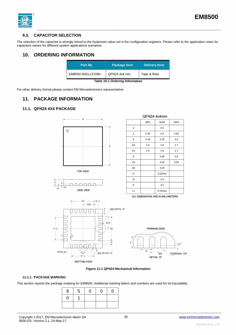
EM8500
Copyright 2017, EM Microelectronic-Marin SA 8500-DS, Version 2.1, 24-May-17
33 www.emmicroelectronic.com
420005-A01, 2.0
9.3. CAPACITOR SELECTION
The selection of the capacitor is strongly linked to the hysteresis value set in the configuration registers. Please refer to the application notes for capacitors values for different system applications scenarios.
10. ORDERING INFORMATION
Part Nb Package form Delivery form
EM8500-A001-LF24B+ QFN24 4x4 mm Tape & Reel
Table 10-1 Ordering Information
For other delivery format please contact EM Microelectronics representative.
11. PACKAGE INFORMATION
11.1. QFN24 4X4 PACKAGE
e/2
L1
e
L
TERMINAL/SIDE
TERMINAL TIP
DETAIL "A"
e SEE DETAIL "A"
bPIN #1 ID
1
2
5 * e
5 * e
D2
D2/2
K
L
E2/2
E2
SEE DETAIL "A"
K
BOTTOM VIEW
A3A1
A
SIDE VIEW
TOP VIEW
D
E
MIN NOM MAX
e
L
b
D2
E2
A
A1
A3
K
D
E
L1
0.45
0.18
2.5
2.5
0.5
0.5
0.25
2.6
2.6
0.85
0.02
0.20
0.20min
4.0
4.0
0.15max
0.55
0.3
2.7
2.7
0.9
0.05
QFN24 4x4mm
ALL DIMENSIONS ARE IN MILLIMETERS
Figure 11-1 QFN24 Mechanical Information
11.1.1. PACKAGE MARKING
This section reports the package marking for EM8500. Additional marking letters and numbers are used for lot traceability.
8 5 0 0 0
0 1
EM8500
Copyright 2017, EM Microelectronic-Marin SA 8500-DS, Version 2.1, 24-May-17
34 www.emmicroelectronic.com
420005-A01, 2.0
EM Microelectronic-Marin SA (“EM”) makes no warranties for the use of EM products, other than those expressly contained in EM's applicable General Terms of Sale, located at http://www.emmicroelectronic.com. EM assumes no responsibility for any errors which may have crept into this document, reserves the right to change devices or specifications detailed herein at any time without notice, and does not make any commitment to update the information contained herein.
No licenses to patents or other intellectual property rights of EM are granted in connection with the sale of EM products, neither expressly nor implicitly.
In respect of the intended use of EM products by customer, customer is solely responsible for observing existing patents and other intellectual property rights of third parties and for obtaining, as the case may be, the necessary licenses.
Important note: The use of EM products as components in medical devices and/or medical applications, including but not limited to, safety and life supporting systems, where malfunction of such EM products might result in damage to and/or injury or death of persons is expressly prohibited, as EM products are neither destined nor qualified for use as components in such medical devices and/or medical applications. The prohibited use of EM products in such medical devices and/or medical applications is exclusively at the risk of the customer.