quicklogic secure digital input/output (sdio) host ... sdio host controller provides a high-speed...
TRANSCRIPT

• • • • • • Proven System Block (PSB) for QuickLogic® Customer Specific Standard Products (CSSPs)
Secure Digital Input/Output (SDIO) Host Controller Data Sheet
Device Highlights
QuickLogic CSSPs are architected from a unique combination of semiconductor solution platforms and PSBs based on customer requirements. This data sheet represents a specific PSB that is available for inclusion in a CSSP. To discuss options for adding this PSB to an existing CSSP, or architecting a new CSSP, contact your QuickLogic Customer Solution Architect (CSA).
The QuickLogic SDIO Host Controller has the following features:
• Compliant with SD Specifications Version 2.xx (Part 1: Physical Layer Specification, v2.00, Part A2: SD Host Controller Standard Specification, v2.00, Part E1: SDIO Specification v2.00, etc.)
• Compliant with MultiMediaCard (MMC) Specification, Version 4.2
• Supports SD/SDIO 1-bit or 4-bit with clock rate up to 50 MHz
• Supports MMC 1-bit, 4-bit or 8-bit with clock rate up to 52 MHz
• Supports Secure Digital High Capacity (SDHC) greater than 2 Gbytes capacity
• High-speed and flexible to support multiple storage options and SDIO peripherals
• Supports SD/SDIO data transfer rate up to 200 Mbits/sec.
• Supports MMC data transfer rate up to 416 Mbits/sec.
• Embedded 512-byte read and write data buffers
• User configurable SD/MMC voltage support
• Power-off capability for SD/SDIO/MMC device by using an external power switch
• Boot from SD, MMC or JC-64 based managed NAND capability
Overview
The SDIO Host Controller PSB provides connectivity between the application processor and an SD/SDIO/MMC card.
The SDIO Host Controller PSB solution addresses the needs of handheld system designs. SD has become one of the leading standards for flash memory cards that are used in smartphones, personal media players, personal navigation devices and digital cameras. The recent addition of SDHC to the SD standard really underscores the strong demand for ever increasing storage capacity. The QuickLogic SDIO Host Controller PSB with SDHC support allows designers to easily connect high capacity SD cards to applications processors.
Target applications for this solution include high capacity storage for navigation systems that hold maps and point-of-interest databases, digital cameras required to hold images, and camcorders that use solid-state recording media. By extending the functionality of the SDIO Host Controller, QuickLogic provides designers with a fast track for adding SDHC compatibility to their products.
SDIO is also one of the leading standards for high-speed peripherals such as WiFi, mobile digital TV and GPS chipsets.
© 2010 QuickLogic Corporation www.quicklogic.com••• •••
1

Secure Digital Input/Output (SDIO) Host Controller Data Sheet Rev. C
2
SDIO Host Controller Architecture
The QuickLogic SDIO Host Controller is fully compatible with the SD Host Controller Standard Specification, Version 2.00 and MMC Specification, Version 4.2.
The SDIO Host Controller main features include:
• Supports clock rate up to 52 MHz
• Supports SD, SDIO and MMC
• Supports I/O commands 52 and 53
• Supports 1-bit and 4-bit data modes
• Supports SDIO device interrupt in 1-bit, 4-bit, and 8-bit modes
• Supports block size up to 512 bytes
The application processor can access the attached SD/SDIO card by writing or reading the SDIO Controller Host Register and Data FIFOs. Figure 1 shows the basic block diagram of the SDIO Host Controller architecture.
Figure 1: SDIO Host Controller Architecture Block Diagram
DAT[3:0]
CMD
Data FIFODAT
Control
CMDControl
HostRegisters
ClockManagement
CardDetection
SDIO Host Controller
WP#
CLK
Processor
SD/SDIOCard
Memory InterfaceSystemInterface
CD#
QuickLogic
www.quicklogic.com © 2010 QuickLogic Corporation•• ••••

Secure Digital Input/Output (SDIO) Host Controller Data Sheet Rev. C
Interface List and Description
Table 1 summarizes the SDIO Host Controller interface signals. The uppercase signals serve as an interface to off-chip components. The lowercase signals serve as an interface to on-chip back-end applications.
Table 1: SDIO Host Controller Interface
Signal Name Direction Description
RESET Input Asynchronous Reset (active high).
SYS_CLK Input System clock.
SD_BCLKX2 Input SD base clock by two.
SD/SDIO Signals
SDIO_ON OutputSD/SDIO power on control:0 = OFF 1 = ON
SDIO_CLK Output SD/SDIO clock.
SDIO_CMD Input/Output SD/SDIO command line.
SDIO_DAT[3:0] Input/Output SD/SDIO data lines.
SDIO_CD InputSD/SDIO Card Detection Pin:0 = Inserted 1 = Not inserted
SDIO_WP InputSD/SDIO Write Protection Pin:0 = Protected 1 = Write enabled
Host Register Interface
cs Input Chip Select
we Input Write Enable
be[x:0] Input Byte Enables
addr[x:0] Input Address Bus
wdata[x:0] Input Write data
rdata[x:0] Output Read data
intr Output Interrupt request to host system
wakeup Output Wakeup request to host system
led Output0 = LED off1 = LED on
© 2010 QuickLogic Corporation www.quicklogic.com• • • •••
3

Secure Digital Input/Output (SDIO) Host Controller Data Sheet Rev. C
4
Register Descriptions
Register TypesTable 2 lists abbreviations for all register types.
NOTE: If the Host Driver writes to RO, ROC, and RSVD registers, it must set the bits to '0' to avoid possible compatibility problems with future SD specifications.
Table 2: Register Type Abbreviations
Register Type Description
RORead-only register. Register bits are read-only and cannot be altered by software or any reset operation. Writes to these bits are ignored.
ROCRead-only status. These bits are initialized to zero at reset. Writes to these bits are ignored.
RWRead-Write register. Register bits are read-write and can be set or cleared by software to the desired state.
RW1CWrite-1-to-clear status. Register bits indicate status when read, a set bit indicating a status event may be cleared by writing a ‘1’. Writing a ‘0’ to RW1C bits has no effect.
RSVDReserved. The bit can be defined for future use and is currently set to ‘0’. These bits must be written as zero.
www.quicklogic.com © 2010 QuickLogic Corporation•• ••••

Secure Digital Input/Output (SDIO) Host Controller Data Sheet Rev. C
SDIO Host Controller RegistersQuickLogic’s SDIO Host Controller is fully compatible with the SD Host Controller Standard Specification, Version 2.00. Table 3 summarizes the SDIO Host Controller register set.
NOTE: For more details on register descriptions and operation sequences, refer to the SD Host Controller Specification, Version 2.0.
The following behaviors apply to the QuickLogic implementation of the SD Host Controller Specification’s SDIO Host Controller registers:
• Read from Not Defined address range returns a random value.
• Read from Data Port (offset 000020h when Buffer Read Enable bit in the Present State Register is ‘0’ has risk of destroying the FIFO logic and not allowed.
• Read from Response registers (offset 000010h – 00001Fh) returns a valid response value only if a command response has been received. It returns a random value if a response value is read after a command without a response is issued. It also returns a random value if the response registers are read before the command response is fully received.
• Block Gap Control Register value is ‘08h’ after reset.
• Capability Register value is fixed and depends on the requirements regarding Voltage Support and Clock Frequency.
Table 3: SDIO Host Controller Register Set
Offset Address[22:0]
Register NameBit31 ------ Bit24 Bit23 ------ Bit16 Bit15 ------ Bit8 Bit7 ------ Bit0
000000h Reserved
000004h Block Count Block Size
000008h Argument00000Ch Command Transfer Mode
000010h Response bit 31 - 0
000014h Response bit 63 - 32000018h Response bit 95 - 64
00001Ch Response bit 127 - 96
000020h Data Port000024h Present State
000028h Wakeup Control Block Gap Control Power Control Host Control
00002Ch Software Reset Timeout Control Clock Control000030h Error Interrupt Status Normal Interrupt Status
000034h Error Interrupt Status Enable Normal Interrupt Status Enable
000038h Error Interrupt Signal Enable Normal Interrupt Signal Enable00003Ch Reserved Auto CMD12 Error Status
000040h Capabilities
000044h Capabilities (Reserved)000048h Maximum Current Capabilities
00004Ch Maximum Current Capabilities (Reserved)
000050h – 0000F8h Not Defined0000FCh Host Controller Version Slot Interrupt Status
© 2010 QuickLogic Corporation www.quicklogic.com• • • •••
5

Secure Digital Input/Output (SDIO) Host Controller Data Sheet Rev. C
6
Table 4 provides a detail description of the Capability Register setting.
Functional and Module Description
The SDIO Host Controller provides a high-speed SD/SDIO/MMC interface to a processor and consists of the following components:
• Host Registers
• Data FIFO
• CMD Control
• DAT Control
• Clock Management
• Power Management and Card Detection
• Synchronization Block
Table 4: Capability Register Settings
Bit Signal Name Value Description
31-27 – 0 Reserved
26 1.8 V support 0 0 = 1.8 V is not supported
25 3.0 V support 0 0 = 3.0 V is not supported
24 3.3 V support 1 1 = 3.3 V is supported
23 Suspend support 1 1 = Suspend and Resume function is supported
22 DMA support 0 0 = DMA function is not supported
21 High-speed support 1 1 = High-speed (50 MHz) is supported
20-18 – 0 Reserved
17-16 Max block length 00b 00b: 512 byte maximum block length
15-14 – 0 Reserved
13-8 Base clock frequency 32h SD/SDIO base clock is 50 MHz
7 Timeout clock unit 1 1 = MHz
6 – 0 Reserved
5-0 Timeout clock frequency 32h Timeout clock frequency is 50 MHz
www.quicklogic.com © 2010 QuickLogic Corporation•• ••••

Secure Digital Input/Output (SDIO) Host Controller Data Sheet Rev. C
Figure 2 shows the SDIO Host Controller sub-module block diagram.
Figure 2: SDIO Host Controller Sub-module Block Diagram
Host Registers The Host Registers block consists of the following components:
• Standard SD/SDIO host register set
• Interrupt logic
• Auto CMD12 logic
The standard SD/SDIO host register set consists of seven parts:
• SD command generation — parameters to generate SD commands
• Response — response value from the card
• Data port — data access port to the internal buffers
• Host controls — host mode control and status
• Interrupt controls — interrupt statuses and enables
• Capabilities — host controller capability information
The Host Controller provides a 32-bit interface and supports byte accesses to the Host Registers. If the system bus is 8 or 16 bits wide, the system interface logic in the SDIO_Wrapper converts it to a 32-bit width.
The Auto CMD12 Logic automatically issues a CMD12 command after the last block of data is transferred if the Auto CMD12 Enable bit in the Transfer Mode register is set.
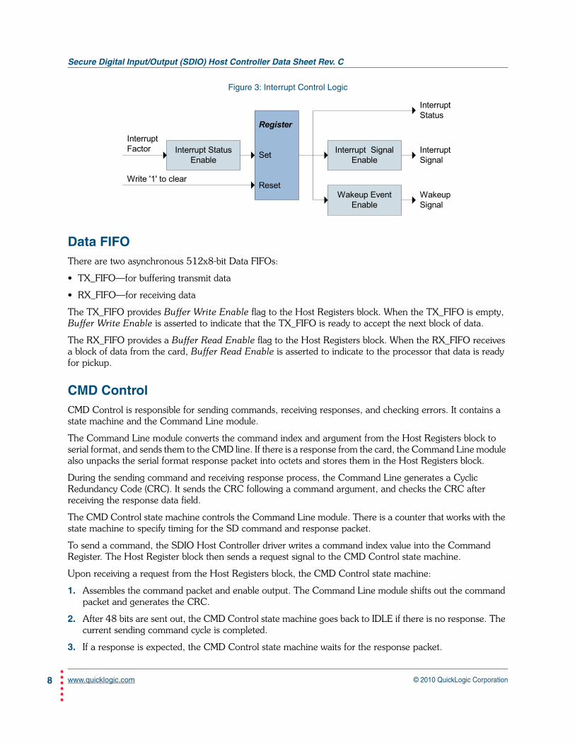
Interrupt control logic consists of interrupt status and enable registers. Figure 3 shows the interrupt control logic.
DAT[3:0]
CMD
Host Registers
SDIO Host Controller
CD#
WP
CLK
System Clock Domain
SD Clock Domain
SD Base Clock Domain
Power Management and
Card Detection
Clock Management
CMD Control
DAT Control
Data FIFO
Sync
Interrupt Logic
AutoCMD12 Logic
SD
IO B
us
FIFO Interface
System Clock
Register Interface
© 2010 QuickLogic Corporation www.quicklogic.com• • • •••
7
Secure Digital Input/Output (SDIO) Host Controller Data Sheet Rev. C
8
Figure 3: Interrupt Control Logic
Data FIFO There are two asynchronous 512x8-bit Data FIFOs:
• TX_FIFO—for buffering transmit data
• RX_FIFO—for receiving data
The TX_FIFO provides Buffer Write Enable flag to the Host Registers block. When the TX_FIFO is empty, Buffer Write Enable is asserted to indicate that the TX_FIFO is ready to accept the next block of data.
The RX_FIFO provides a Buffer Read Enable flag to the Host Registers block. When the RX_FIFO receives a block of data from the card, Buffer Read Enable is asserted to indicate to the processor that data is ready for pickup.
CMD ControlCMD Control is responsible for sending commands, receiving responses, and checking errors. It contains a state machine and the Command Line module.
The Command Line module converts the command index and argument from the Host Registers block to serial format, and sends them to the CMD line. If there is a response from the card, the Command Line module also unpacks the serial format response packet into octets and stores them in the Host Registers block.
During the sending command and receiving response process, the Command Line generates a Cyclic Redundancy Code (CRC). It sends the CRC following a command argument, and checks the CRC after receiving the response data field.
The CMD Control state machine controls the Command Line module. There is a counter that works with the state machine to specify timing for the SD command and response packet.
To send a command, the SDIO Host Controller driver writes a command index value into the Command Register. The Host Register block then sends a request signal to the CMD Control state machine.
Upon receiving a request from the Host Registers block, the CMD Control state machine:
1. Assembles the command packet and enable output. The Command Line module shifts out the command packet and generates the CRC.
2. After 48 bits are sent out, the CMD Control state machine goes back to IDLE if there is no response. The current sending command cycle is completed.
3. If a response is expected, the CMD Control state machine waits for the response packet.
Interrupt StatusEnable
Register
Set
Reset
Interrupt SignalEnable
Wakeup EventEnable
InterruptStatus
InterruptSignal
WakeupSignal
InterruptFactor
Write '1' to clear
www.quicklogic.com © 2010 QuickLogic Corporation•• ••••

Secure Digital Input/Output (SDIO) Host Controller Data Sheet Rev. C
4. If response does not come within 64 clock cycles, the CMD Control state machine goes to IDLE and issues a timeout error interrupt.
5. After receiving the first bit of the response packet, the CMD Control state machine starts to count the number of bits received. The Command Line module converts the incoming serial data into parallel data, checks the command index field, generates a CRC, and verifies the received CRC value.
6. Based on the response packet type, the CMD Control state machine ends response packet reception after either 48 or 136 bits.
The CMD Control state machine also provides command end and response end status to DAT Control so that it can start data transfer based on the transfer mode settings.
DAT Control DAT Control is responsible for transferring data between the Data FIFO and the SD data bus, and for detecting the SDIO interrupt. It consists of an SD data multiplexer, a state machine, and DAT Line sub-modules.
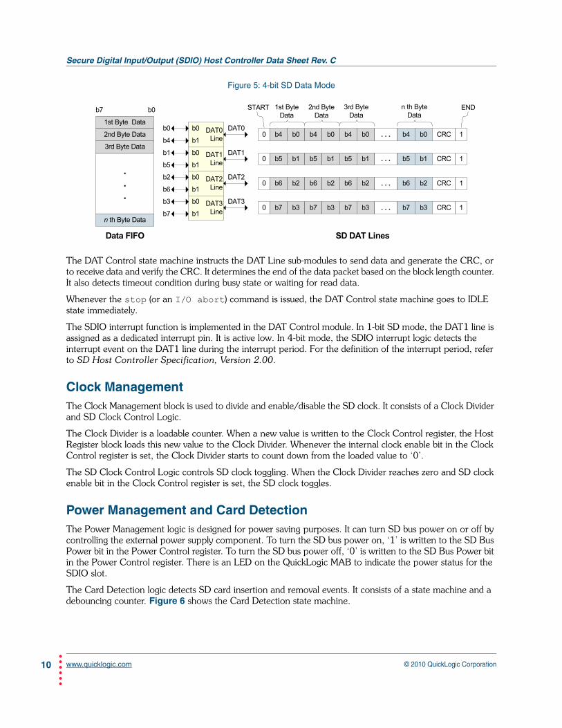
The SD data multiplexer supports 1-bit and 4-bit SD/SDIO modes. In 1-bit mode, only DAT0 is used. All 8-bit data from the Data FIFO connects to the DAT0 Line sub-module in the following way: bit0 from the Data FIFO connects to bit0 of the DAT0 Line module, bit1 from the Data FIFO connects to bit1 of the DAT0 Line module, etc. The data bit sequence on the SD data line is shown in Figure 4.
Figure 4: 1-bit SD Data Mode
In 4-bit mode, all four SD data lines DAT [3:0] are used. Figure 5 shows data connections between the Data FIFO and four DAT Line modules in 4-bit mode. The data sequence in 4-bit mode is also shown.
Data FIFO
DAT0Line
DAT0
START
b0
b1
b2
b3
b4
b5
b6
b7
b0
b1
b2
b3
b4
b5
b6
b7
SD DAT0 Line
01st Byte
Data2nd Byte
Data3rd Byte
Data . . . n th ByteData
CRC 1
END
b7 b6 b5 b4 b3 b2 b1 b0
b7 b6 b5 b4 b3 b2 b1 b0
1st Byte Data
2nd Byte Data
3rd Byte Data
.
.
.
n th Byte Data
b7 b0
© 2010 QuickLogic Corporation www.quicklogic.com• • • •••
9
Secure Digital Input/Output (SDIO) Host Controller Data Sheet Rev. C
10
Figure 5: 4-bit SD Data Mode
The DAT Control state machine instructs the DAT Line sub-modules to send data and generate the CRC, or to receive data and verify the CRC. It determines the end of the data packet based on the block length counter. It also detects timeout condition during busy state or waiting for read data.
Whenever the stop (or an I/O abort) command is issued, the DAT Control state machine goes to IDLE state immediately.
The SDIO interrupt function is implemented in the DAT Control module. In 1-bit SD mode, the DAT1 line is assigned as a dedicated interrupt pin. It is active low. In 4-bit mode, the SDIO interrupt logic detects the interrupt event on the DAT1 line during the interrupt period. For the definition of the interrupt period, refer to SD Host Controller Specification, Version 2.00.
Clock Management The Clock Management block is used to divide and enable/disable the SD clock. It consists of a Clock Divider and SD Clock Control Logic.
The Clock Divider is a loadable counter. When a new value is written to the Clock Control register, the Host Register block loads this new value to the Clock Divider. Whenever the internal clock enable bit in the Clock Control register is set, the Clock Divider starts to count down from the loaded value to ‘0’.
The SD Clock Control Logic controls SD clock toggling. When the Clock Divider reaches zero and SD clock enable bit in the Clock Control register is set, the SD clock toggles.
Power Management and Card DetectionThe Power Management logic is designed for power saving purposes. It can turn SD bus power on or off by controlling the external power supply component. To turn the SD bus power on, ‘1’ is written to the SD Bus Power bit in the Power Control register. To turn the SD bus power off, ‘0’ is written to the SD Bus Power bit in the Power Control register. There is an LED on the QuickLogic MAB to indicate the power status for the SDIO slot.
The Card Detection logic detects SD card insertion and removal events. It consists of a state machine and a debouncing counter. Figure 6 shows the Card Detection state machine.
Data FIFO
DAT0
START
b0
b1
b0
b1
b0
b1
b0
b1
b0
b4
b1
b5
b2
b6
b3
b7
SD DAT Lines
1st Byte Data
2nd Byte Data
3rd Byte Data
.
.
.
n th Byte Data
b7 b0
0 b4 b0 b4 b0 b4 b0 . . . b4 b0 CRC 1
0 b5 b1 b5 b1 b5 b1 . . . b5 b1 CRC 1
0 b6 b2 b6 b2 b6 b2 . . . b6 b2 CRC 1
0 b7 b3 b7 b3 b7 b3 . . . b7 b3 CRC 1
DAT0Line
DAT1Line
DAT2Line
DAT3Line
DAT1
DAT2
DAT3
1st ByteData
2nd ByteData
3rd ByteData
n th ByteData
END
www.quicklogic.com © 2010 QuickLogic Corporation•• ••••

Secure Digital Input/Output (SDIO) Host Controller Data Sheet Rev. C
Figure 6: Card Detection Finite State Machine
The state machine starts in Reset state at power-on and changes to the Debouncing state once the debouncing clock is valid. In the Debouncing state, provided that the SDIO_CD signal is stable for more than 256 clocks, the state changes to a Card Inserted state if SDIO_CD is ‘0’ or to No Card if SDIO_CD is ‘1’. If the card is removed, the state machine immediately moves from Card Inserted state to Debouncing state. In the same way, when the card is inserted, the state machine moves from No Card state to Debouncing state.
Synchronization BlockThe Sync block is used to synchronize the signals across different clock domains. It also provides a pulse signal based on the source T-flop signal’s transition.
Booting from SD/MMC/Managed NAND
QuickLogic has implemented a boot interface to managed NAND using its SDIO Host Controller device. This device offers configurable interfaces, making it adaptable for use with most processor families, as well as for use with SD, SDHC, MMC, and managed NAND memories. For processors already possessing these interfaces, the SDIO Host controller expands their capacity as well as offering boot capability.
The solution to boot from managed NAND needs two parts: a hardware component and a software component. The hardware component includes a Boot Controller and 2 K embedded SRAM. After the Reset signal, the Boot Controller loads the first four sectors of the managed NAND device to the SRAM. The software component is an initial program loader (IPL) routine that performs minimal CPU initialization and transfers the boot loader code from the managed NAND to the processor. Working together, these two components can take the system past the initial chicken-and-egg situation of needing software in order to load the software, allowing the managed NAND to serve both as program and data storage.
The QuickLogic implementation is a tested, proven solution. It has demonstrated that it can perform an entire boot sequence under both Linux and Windows® CE operating systems using a variety of application processors. It has been tested with various SD, SDHC, MMC, and managed NAND devices and has built-in autodetection of the memory interface to perform the proper device initialization sequence. This solution can easily be ported to all major application processors.
Booting from managed NAND imposes both hardware and software requirements on a design. The hardware requirements, shown in Figure 7, include a connection to the boot chip select line coming from the processor as well as control of the reset line. The reset line control allows the Host Controller to prevent the CPU from
Reset Debouncing
No Card
Card Inserted
DebouncingClock valid
SDIO_CD=1
SDIO_CD=0
© 2010 QuickLogic Corporation www.quicklogic.com• • • •••
11

Secure Digital Input/Output (SDIO) Host Controller Data Sheet Rev. C
12
operating until the managed NAND boot interface is ready. The boot chip select line’s memory interface configuration is also reconfigured after power-up to support the use of a READY signal to gate access to memory.
Figure 7: QuickLogic’s SDIO Host Controller Booting Process.
One software requirement is the development of an IPL program specific to the processor being used. The RAM capacity of the SDIO Host Controller, 2048 bytes, dictates that the IPL program be limited to 512 instructions, assuming a 32-bit processor. The IPL code thus must be optimized for the CPU and architecture it is to support. While 512 instructions is a small program space, it is an adequate size, especially if the processor also has on-chip RAM available for holding stacks and variables. The processor’s on-chip RAM is also useful for storing and running the boot loader program later in the process.
The IPL code is not the only software that must be adapted to the processor and architecture used in the design. The system’s Boot Loader code must be adapted so that the processor executes the code out of its internal RAM rather than external ROM. It must also support reading the code through the managed NAND memory interface. Similarly, the operating system will require drivers to be able to use the SDIO Host Controller to its full capability once the system has booted.
Three-Stage Boot Process
With both the software and hardware elements in place, the boot process follows a three step operation.
1. At power-up, the Host Controller keeps the processor in a reset state while it downloads the IPL code from managed NAND into its internal RAM. It then maps its internal RAM to serve as SRAM to the processor under control of the processor’s boot address chip select and releases the CPU from its reset state.
2. Once released, the CPU begins executing the IPL from the Host Controller’s RAM. The IPL code uses the Host Controller to load the Boot Loader code into the processor’s internal SRAM. The IPL then jumps to that SRAM address to begin the execution of the Boot Loader.
3. The Boot Loader initializes system SDRAM, and then loads the operating system from the managed NAND into system SDRAM. Once the OS is loaded, program execution jumps to the OS, concluding the boot process.
After the boot process is complete, the remainder of the managed NAND device (the portion not containing the boot software) can be accessed by the OS as a storage device within the file system. The amount of the managed NAND device required to contain the boot software (the IPL, Boot Loader and OS image) is very small – on the order of 64 Mbytes. The managed NAND device can be partitioned and formatted so that the remaining majority of the device can be accessed as user storage, while the 64 Mbyte boot portion of the managed NAND device is protected and kept secure by design.
ApplicationProcessor
SDMemoryReset
HostController
Host Controller
www.quicklogic.com © 2010 QuickLogic Corporation•• ••••

Secure Digital Input/Output (SDIO) Host Controller Data Sheet Rev. C
Using an approach such as this gives designers many benefits. To begin with, it simplifies board design and saves parts cost. Using managed NAND for both program and data storage eliminates the need for a separate NOR device. In addition, the interface to managed NAND uses fewer I/O lines, requiring only 6 lines versus 16 or more, for a conventional memory interface. These I/O resources are then available for other uses in the design.
Since the managed NAND offers standard, vendor-agnostic interfaces, designers have more supply options open to them. They can go with MMC or SD memory devices, both of which have JEDEC-standard pinouts, and have a wide range of suppliers from which to choose. Unlike raw NAND Flash, there is no vendor-specific software required in the design.
The QuickLogic SDIO Host Controller can also connect to multiple SD-based managed NAND devices simultaneously, as the controller can be customized to include a multiplexing structure for multiple SD devices or can be compatible with a multi-load MMC bus. This allows designers to mix and match memory suppliers and densities in their system designs to minimize bill of materials cost while precisely satisfying design requirements. For example, in a PND device, design requirements may call for 3 Gbytes of storage to accommodate map and point of interest data. To satisfy this requirement, a designer would typically choose a 4 Gbyte managed NAND device, but with the QuickLogic SDIO Host Controller solution, the designer now has the option of choosing a less expensive two-chip approach of 2 Gbytes + 1 Gbyte.
Using managed NAND also helps future-proof their design as increasing demands for memory capacity move storage requirements above 4 Gbytes. The standard interfaces of managed NAND hide the complexity of multi-level circuits, allowing designers to double memory capacity simply by changing to the new technology. The configurable nature of the SDIO Host Controller also ensures that developers can move to SDHC (high capacity) memories as needed. Such a move would be complicated when using raw NAND Flash because the higher density devices use block-oriented addressing rather than the byte-oriented addressing that processors expect. File structures for high-density devices also move, from FAT16 to FAT32, further complicating adoption of high density. The QuickLogic Complete Connectivity Solution for managed NAND boot accommodates all of these changes with the same hardware design, ensuring that designers can migrate to higher memory capacities with minimal effort.
managed NAND thus makes an excellent match to the system requirements. It offers the high density benefits of NAND Flash with the boot capability of NOR Flash in a single memory device. It also provides a vendor-agnostic interface, increasing supply options, and reduces software overhead as compared to raw Flash memories.
QuickLogic’s configurable SDIO Host Controller is an ideal solution for system developers as well. Its capacity and flexibility gives designers their choice of processor and memory bus interface types while providing additional I/O to the system along with the bootable managed NAND function. It also helps future proof designs by providing access to higher-density memory with minimal system changes.
Booting from managed NAND thus provides a compelling third option to the two types of Flash memory currently being used in designs. It offers cost savings, design simplification, and the capability of handling increasing memory densities. It also provides the ability to mix and match vendors, eliminating sole-source supply, and to mix and match memory densities using multiplexed SD or multiple-chip MMC designs. All these benefits translate into faster design times for current and future device generations, as well as reducing BOM costs in the highly dynamic and competitive mobile market.
© 2010 QuickLogic Corporation www.quicklogic.com• • • •••
13
Secure Digital Input/Output (SDIO) Host Controller Data Sheet Rev. C
14
Supported Operating Systems
The SDIO Host Controller PSB supports the following operating systems:
• Windows® CE
• Windows Mobile®
• Linux®
• Android®
Contact Information
Phone: (408) 990-4000 (US)
(647) 367-1014 (Canada)
+(44) 1932-21-3160 (Europe)
+(886) 2-2345-5600 (Taiwan)
+(86) 21-5116-0532 (China)
E-mail: [email protected]
Sales: [email protected]
Support: www.quicklogic.com/support
Internet: www.quicklogic.com
Revision History
Notice of Disclaimer
QuickLogic is providing this design, product or intellectual property "as is." By providing the design, product or intellectual property as one possible implementation of your desired system-level feature, application, or standard, QuickLogic makes no representation that this implementation is free from any claims of infringement and any implied warranties of merchantability or fitness for a particular purpose. You are responsible for obtaining any rights you may require for your system implementation. QuickLogic shall not be liable for any damages arising out of or in connection with the use of the design, product or intellectual property including liability for lost profit, business interruption, or any other damages whatsoever. QuickLogic products are not designed for use in life-support equipment or applications that would cause a life-threatening situation if any such products failed. Do not use QuickLogic products in these types of equipment or applications.
Revision Date Originator and Comments
A April 2008 Howard Li and Kathleen Murchek
B April 2008 Alex Paskovatyi, Stanley Hung, James Deihl and Kathleen Murchek
C July 2010 Kathleen Bylsma
www.quicklogic.com © 2010 QuickLogic Corporation•• ••••

Secure Digital Input/Output (SDIO) Host Controller Data Sheet Rev. C
QuickLogic does not assume any liability for errors which may appear in this document. However, QuickLogic attempts to notify customers of such errors. QuickLogic retains the right to make changes to either the documentation, specification, or product without notice. Verify with QuickLogic that you have the latest specifications before finalizing a product design.
Copyright and Trademark Information
Copyright © 2010 QuickLogic Corporation. All Rights Reserved.
The information contained in this document and is protected by copyright. All rights are reserved by QuickLogic Corporation. QuickLogic Corporation reserves the right to modify this document without any obligation to notify any person or entity of such revision. Copying, duplicating, selling, or otherwise distributing any part of this product without the prior written consent of an authorized representative of QuickLogic is prohibited.
QuickLogic is a registered trademark; and the QuickLogic logo is a trademark of QuickLogic. Other trademarks are the property of their respective companies.
© 2010 QuickLogic Corporation www.quicklogic.com• • • •••
15