quantum electronic transport in mesoscopic graphene devices
TRANSCRIPT

Quantum Electronic Transport in Mesoscopic Graphene Devices
CitationAllen, Monica Theresa. 2016. Quantum Electronic Transport in Mesoscopic Graphene Devices. Doctoral dissertation, Harvard University, Graduate School of Arts & Sciences.
Permanent linkhttp://nrs.harvard.edu/urn-3:HUL.InstRepos:33493258
Terms of UseThis article was downloaded from Harvard University’s DASH repository, and is made available under the terms and conditions applicable to Other Posted Material, as set forth at http://nrs.harvard.edu/urn-3:HUL.InstRepos:dash.current.terms-of-use#LAA
Share Your StoryThe Harvard community has made this article openly available.Please share how this access benefits you. Submit a story .
Accessibility

Quantum Electronic Transport in Mesoscopic Graphene
Devices
A dissertation presented
by
Monica Theresa Allen
to
The Department of Physics
in partial fulfillment of the requirements
for the degree of
Doctor of Philosophy
in the subject of
Physics
Harvard University
Cambridge, Massachusetts
April 2016

c©2016 - Monica Theresa Allen
All rights reserved.

Dissertation Advisor: Author:
Professor Amir Yacoby Monica Theresa Allen
Quantum Electronic Transport in Mesoscopic Graphene Devices
Abstract
Graphene provides a rich platform for the study of interaction-induced broken
symmetry states due to the presence of spin and sublattice symmetries that can be con-
trollably broken with external electric and magnetic fields. At high magnetic fields and low
temperatures, where quantum effects dominate, we map out the phase diagram of broken
symmetry quantum Hall states in suspended bilayer graphene. Application of a perpendicu-
lar electric field breaks the sublattice (or layer) symmetry, allowing identification of distinct
layer-polarized and canted antiferromagnetic ν = 0 states. At low fields, a new spontaneous
broken-symmetry state emerges, which we explore using transport measurements.
The large energy gaps associated with the ν = 0 state and electric field induced
insulating states in bilayer graphene offer an opportunity for tunable bandgap engineering.
We use local electrostatic gating to create quantum confined devices in graphene, including
quantum point contacts and gate-defined quantum dots.
The final part of this thesis focuses on proximity induced superconductivity in
graphene Josephson junctions. We directly visualize current flow in a graphene Josephson
junction using superconducting interferometry. The key to our approach involves recon-
struction of the real-space current density from magnetic interference using Fourier meth-
ods. We observe that current is confined to the crystal boundaries near the Dirac point and
that edge and bulk currents coexist at higher Fermi energies. These results are consistent
with the existence of “fiber-optic” edge modes at the Dirac point, which we model theoret-
iii

Abstract
ically. Our techniques also open the door to fast spatial imaging of current distributions
along more complicated networks of domains in larger crystals.
iv

Contents
Title Page . . . . . . . . . . . . . . . . . . . . . . . . . . . . . . . . . . . . . . . . iAbstract . . . . . . . . . . . . . . . . . . . . . . . . . . . . . . . . . . . . . . . . . iiiTable of Contents . . . . . . . . . . . . . . . . . . . . . . . . . . . . . . . . . . . . vList of Figures . . . . . . . . . . . . . . . . . . . . . . . . . . . . . . . . . . . . . viiList of Tables . . . . . . . . . . . . . . . . . . . . . . . . . . . . . . . . . . . . . . ixCitations to Previously Published Work . . . . . . . . . . . . . . . . . . . . . . . xAcknowledgments . . . . . . . . . . . . . . . . . . . . . . . . . . . . . . . . . . . . xi
1 Introduction 11.1 Monolayer and bilayer graphene . . . . . . . . . . . . . . . . . . . . . . . . . 11.2 The quantum Hall effect in graphene and interaction-driven broken symmetry
states . . . . . . . . . . . . . . . . . . . . . . . . . . . . . . . . . . . . . . . 41.3 Proximity induced superconductivity in a graphene Josephson junction . . . 71.4 Outline of this thesis . . . . . . . . . . . . . . . . . . . . . . . . . . . . . . . 11
2 Broken symmetry states in dual-gated suspended bilayer graphene 142.1 Overview . . . . . . . . . . . . . . . . . . . . . . . . . . . . . . . . . . . . . 142.2 Degeneracies in monolayer and bilayer graphene . . . . . . . . . . . . . . . . 152.3 Electric field tunable gap in suspended bilayers . . . . . . . . . . . . . . . . 162.4 Evolution of Landau levels in electric field . . . . . . . . . . . . . . . . . . . 182.5 Phase diagram of the ν = 0 state . . . . . . . . . . . . . . . . . . . . . . . . 222.6 Spontaneous gapped phase in bilayer graphene at zero field . . . . . . . . . 242.7 Device fabrication . . . . . . . . . . . . . . . . . . . . . . . . . . . . . . . . 27
3 Gate defined quantum confinement in suspended bilayer graphene 293.1 Overview . . . . . . . . . . . . . . . . . . . . . . . . . . . . . . . . . . . . . 293.2 Quantum confinement in graphene . . . . . . . . . . . . . . . . . . . . . . . 303.3 Device overview . . . . . . . . . . . . . . . . . . . . . . . . . . . . . . . . . . 323.4 Quantum confinement at zero magnetic field . . . . . . . . . . . . . . . . . . 323.5 Coulomb blockade in the quantum Hall regime . . . . . . . . . . . . . . . . 353.6 Geometric control over Coulomb blockade period . . . . . . . . . . . . . . . 363.7 Methods . . . . . . . . . . . . . . . . . . . . . . . . . . . . . . . . . . . . . . 413.8 Extended Discussion . . . . . . . . . . . . . . . . . . . . . . . . . . . . . . . 43
v

Contents
4 Spatially resolved edge currents in monolayer and bilayer graphene 474.1 Overview . . . . . . . . . . . . . . . . . . . . . . . . . . . . . . . . . . . . . 474.2 Guided-wave electronic states in graphene . . . . . . . . . . . . . . . . . . . 484.3 Experiment: spatial imaging of current flow using Josephson interferometry 494.4 Extended Discussion . . . . . . . . . . . . . . . . . . . . . . . . . . . . . . . 59
4.4.1 Modeling electronic guided modes . . . . . . . . . . . . . . . . . . . 594.4.2 Josephson junctions: Device overview . . . . . . . . . . . . . . . . . 734.4.3 Fourier method for extraction of supercurrent density distribution . 744.4.4 Gaussian fits to extract edge state widths . . . . . . . . . . . . . . . 764.4.5 Edge versus bulk amplitudes . . . . . . . . . . . . . . . . . . . . . . 764.4.6 Bayesian method for extraction of supercurrent density distribution 774.4.7 Normal state device characterization . . . . . . . . . . . . . . . . . . 82
5 Visualization of phase-coherent electron interference in a ballistic grapheneJosephson junction 855.1 Overview . . . . . . . . . . . . . . . . . . . . . . . . . . . . . . . . . . . . . 855.2 Electron optics in ballistic graphene . . . . . . . . . . . . . . . . . . . . . . 865.3 Superconducting transport in a ballistic graphene Josephson junction . . . . 885.4 Modulation of multiple Andreev reflection intensity using cavity resonances 935.5 Visualization of edge and bulk current flow using Josephson interferometry 955.6 Model of superconducting interference in the presence of guided edge states 975.7 Extended Discussion . . . . . . . . . . . . . . . . . . . . . . . . . . . . . . . 100
A Supplementary Figures 111A.1 Supplementary Figures for Chapter 3 . . . . . . . . . . . . . . . . . . . . . . 111A.2 Supplementary Figures for Chapter 4 . . . . . . . . . . . . . . . . . . . . . . 118A.3 Supplementary Figures for Chapter 5 . . . . . . . . . . . . . . . . . . . . . . 120
B Fabrication of Suspended Graphene Devices 125B.1 Fabrication of dual-gated suspended bilayer graphene . . . . . . . . . . . . . 125B.2 Current annealing procedure for graphene . . . . . . . . . . . . . . . . . . . 126
C Preparation of graphene - boron nitride layered heterostructures 128C.1 Piranha cleaning recipe for wafers . . . . . . . . . . . . . . . . . . . . . . . . 128C.2 Flake pick-up procedure for assembly of van der Waals heterostructures . . 129C.3 Exfoliation of MoS2 . . . . . . . . . . . . . . . . . . . . . . . . . . . . . . . 130
Bibliography 131
vi

List of Figures
1.1 Band structure of monolayer graphene . . . . . . . . . . . . . . . . . . . . . 21.2 Pseudospin-momentum locking in monolayer and bilayer graphene . . . . . 41.3 The band structure of bilayer graphene . . . . . . . . . . . . . . . . . . . . . 51.4 Quantum Hall effect in monolayer and bilayer graphene . . . . . . . . . . . 61.5 Andreev reflection at the graphene-superconductor interface . . . . . . . . . 81.6 Electrodynamics of a Josephson junction . . . . . . . . . . . . . . . . . . . . 8
2.1 Broken layer symmetry in suspended dual-gated bilayer graphene . . . . . . 172.2 Evolution of Landau levels in electric field . . . . . . . . . . . . . . . . . . . 192.3 Phase diagram of competing ordered states at charge neutrality . . . . . . . 232.4 Experimental evidence of a spontaneous gap in suspended bilayer graphene 26
3.1 Suspended gate-defined bilayer graphene quantum dot . . . . . . . . . . . . 333.2 Coulomb blockade at B = 0 . . . . . . . . . . . . . . . . . . . . . . . . . . . 353.3 Coulomb blockade at B = 5.2 T . . . . . . . . . . . . . . . . . . . . . . . . . 373.4 Geometric control over Coulomb blockade period . . . . . . . . . . . . . . . 38
4.1 ‘Fiber-optic’ modes and spatially resolved current imaging in a grapheneJosephson junction . . . . . . . . . . . . . . . . . . . . . . . . . . . . . . . . 53
4.2 Gate-tunable evolution of edge and bulk current-carrying states in graphene 544.3 Boundary currents in bilayer graphene in the presence of broken crystal in-
version symmetry . . . . . . . . . . . . . . . . . . . . . . . . . . . . . . . . . 554.4 ‘Fiber-optics’ theoretical model of transport in graphene . . . . . . . . . . . 604.5 Spatially-resolved density of states (DOS) for guided modes in MLG obtained
for a delta-function line potential model . . . . . . . . . . . . . . . . . . . . 684.6 Bayesian estimation method for extracting the current distribution . . . . . 804.7 Bayesian estimation results: ratio of the supercurrent carried by the edge
states as a function of carrier density . . . . . . . . . . . . . . . . . . . . . . 804.8 Bayesian method for extraction of asymmetric current distributions . . . . . 824.9 Normal resistance characterization and ballistic supercurrent propagation in
graphene Josephson junctions . . . . . . . . . . . . . . . . . . . . . . . . . . 83
vii

List of Figures
5.1 Normal state signatures of electron wave interference in a graphene Fabry-Perot cavity . . . . . . . . . . . . . . . . . . . . . . . . . . . . . . . . . . . . 89
5.2 Interplay between superconductivity and the Fabry-Perot interference in aballistic graphene Josephson junction . . . . . . . . . . . . . . . . . . . . . . 92
5.3 Spatially resolved supercurrent imaging in a ballistic graphene cavity . . . . 965.4 Theoretical model of edge and bulk interference in the ballistic regime . . . 98
A.1 Scanning electron micrographs of gate defined quantum dots in graphene . 111A.2 Broken symmetry quantum Hall states in local gated graphene devices . . . 112A.3 Graphene quantum point contacts defined by local gating . . . . . . . . . . 113A.4 Conductance through a quantum point contact at nonzero source-drain bias 114A.5 Coulomb diamonds and even-odd effect at B=0 . . . . . . . . . . . . . . . . 115A.6 Quantum confinement in device D3 . . . . . . . . . . . . . . . . . . . . . . 116A.7 Quantum dot size determined by simulations . . . . . . . . . . . . . . . . . 117A.8 Characterization of proximity induced superconductivity in a bilayer graphene
Josephson junction . . . . . . . . . . . . . . . . . . . . . . . . . . . . . . . . 118A.9 Additional superconducting interferometry plots for device ML1, showing
edge to bulk transition in real space over a large range of carrier density . . 119A.10 Additional superconducting interferometry plots for device BL3 . . . . . . . 119A.11 Ballistic resistance oscillations in a gate-defined Fabry-Perot interferometer
on hBN . . . . . . . . . . . . . . . . . . . . . . . . . . . . . . . . . . . . . . 120A.12 Nontrivial current flow through a graphene Fabry-Perot resonator, as re-
vealed by Fraunhofer interferometry . . . . . . . . . . . . . . . . . . . . . . 121A.13 Dependence of normalized Fraunhofer interference on cavity resonances in
additional samples . . . . . . . . . . . . . . . . . . . . . . . . . . . . . . . . 121A.14 Interplay between multiple Andreev reflection and cavity resonances in an
additional device . . . . . . . . . . . . . . . . . . . . . . . . . . . . . . . . . 122A.15 Additional multiple Andreev reflection data sets from sample B3 . . . . . . 123A.16 Experimental dependence of multiple Andreev reflection amplitude on cavity
interferences . . . . . . . . . . . . . . . . . . . . . . . . . . . . . . . . . . . . 123A.17 Theoretical dependence of multiple Andreev reflection amplitude on cavity
transmission . . . . . . . . . . . . . . . . . . . . . . . . . . . . . . . . . . . . 124
viii

List of Tables
3.1 Measured quantum dot sizes from Coulomb blockade fits . . . . . . . . . . . 393.2 Simulated dot sizes obtained from Models 1 and 2 . . . . . . . . . . . . . . 40
4.1 List of device dimensions for graphene Josephson junctions . . . . . . . . . 50
ix

Citations to Previously Published Work
Large portions of Chapter 2 have appeared in the following paper:
“Broken-symmetry states in doubly gated suspended bilayer graphene”. R.T.Weitz, M.T. Allen, B.E. Feldman, J. Martin, and A. Yacoby. Science 330,812-816 (2010)
Chapter 3 appears in its entirety as
“Gate-defined quantum confinement in suspended bilayer graphene.” M. T.Allen, J. Martin, A. Yacoby. Nature Communications 3:934 (2012).
The material covered in Chapter 4 appears in
“Spatially resolved edge currents and guided-wave electronic states in graphene.”M. T. Allen, O. Shtanko, I. C. Fulga, A. R. Akhmerov, K. Watanabe, T.Taniguchi, P. Jarillo-Herrero, L. S. Levitov, and A. Yacoby. Nature Physics,12, 128-133 (2016).
The material covered in Chapter 5 appears in
“Visualization of phase-coherent electron interference in a ballistic grapheneJosephson junction.” M. T. Allen, O. Shtanko, I. C. Fulga, J. Wang, D. Nur-galiev, K. Watanabe, T. Taniguchi, A. R. Akhmerov, P. Jarillo-Herrero, L. S.Levitov, and A. Yacoby. arXiv:1506.06734 (2015).
Electronic preprints are available on the Internet at the following URL:
http://arXiv.org
x

Acknowledgments
First, I would like to thank Amir Yacoby for his scientific guidance, stimulating
discussions, and for giving me the freedom and resources to explore of a range of new
phenomena in graphene. In addition to having a strong theoretical background, Amir is a
creative experimentalist who provided the inspiration behind many of the ideas explored in
this thesis. I would also like to thank my thesis committee, Robert Westervelt and Ronald
Walsworth, for their advice, support, and interest in my progress.
Leonid Levitov deserves special recognition for his insights on our work on broken
symmetry quantum Hall states and theoretical contributions on the induced superconduc-
tivity experiments. I am also grateful to Pablo Jarillo-Herrero and Philip Kim and their
students for stimulating discussions, particularly regarding hBN device fabrication.
I would like to thank my research collaborators, including Jens Martin, who men-
tored me as an undergraduate and during the early stages of my PhD, as well as Thomas
Weitz and Ben Feldman, who worked closely with me on the investigation of correlated
electron states in suspended bilayer graphene devices. I had the privilege of working di-
rectly with several theory students and postdocs, including Oles Shtanko, Ion Cosma Fulga,
Anton Akhmerov, and Daniyar Nurgaliev. I also appreciate fruitful discussions with Pro-
fessors Bertrand Halperin, Allan MacDonald, Jay Deep Sau, Dima Abanin, and Rahul
Nandkishore.
Within the Yacoby lab, I benefited from the technical expertise of Vivek Venkat-
achalam, Hendrik Bluhm, and Oliver Dial. I’d also like to thank postdocs Marc Warner,
Francesco Casola, Patrick Maletinksy, Toeno van der Sar, Kristaan de Greve, and Lan
Luan, as well as graduate students Andrei Levin, Gilad Barak, Gilad Ben-Shach, Sungkun
Hong, Tony Zhou, Mike Grinolds, Sandra Foletti, Michael Schulman, Sean Hart, Hechen
Ren, Shannon Harvey, Yuliya Dovgenko, Di Wei, Lucas Orona, and Michael Kosowsky.
Thanks to Jimmy Williams, Hugh Churchill, Patrick Herring, Yongjie Hu, and Ferdinand
xi

Acknowledgments
Keummeth from the Marcus lab. I also appreciate discussions with the Kim lab and Jarillo-
Herrero lab, especially Patrick Maher, Carlos Forsythe, Xiaomeng Liu, Hadar Steinberg,
Javier Sanchez-Yamagishi, Valla Fatemi, Joel Wang, and Britt Baugher. I would also like to
acknowledge the important contributions of our boron nitride crystal growers, K. Watanabi
and T. Taniguchi.
I extend special thanks to Giorgio Frossati, for his technical expertise and pa-
tience when troubleshooting issues with the Frossati dilution refrigerator remotely from the
Netherlands. Many thanks to the attentive staff of the Harvard Center for Nanoscale Sys-
tems, especially Jiangdong Deng, Yuan Lu, Ling Xie, and Jason Tresback. I am grateful to
our administrative staff, including Yacoby lab administrators Carolyn Moore and Hannah
Belcher, as well as the physics department graduate administrator Lisa Cacciabaudo.
During graduate school I was generously supported by the Purcell Fellowship at
Harvard and the DOE Office of Science Graduate Fellowship (DOE-SCGF).
I’d like to thank everyone who made my graduate school experience more pleasant.
I’m grateful to Jen, Van, Mikhail, Kirill, and Nike for many years of friendship and company.
Finally, I would like to thank Shrenik, Andrew, and my parents for their love and support.
xii

Chapter 1
Introduction
1.1 Monolayer and bilayer graphene
Monolayer graphene is a two dimensional sheet of carbon atoms arranged in a hon-
eycomb lattice [1,2]. These atoms are connected by hybridized sp2 orbitals within the plane,
while mobile electrons in the out-of-plane pz orbitals are responsible for the high conduc-
tivity of graphene. There are two relevant symmetries for graphene: the conventional spin
of electrons and a pseudospin associated with relative weight of the electronic wavefunction
on the two sublattices, A and B (see Fig. 1.1). The lattice unit vectors are a1 = a2 (3,√
3)
and a2 = a2 (3,−
√3), where a = 1.42A is the distance between nearest-neighbor carbon
atoms, and the reciprocal vectors are b1 = 2π3a (1,
√3) and b2 = 2π
3a (1,−√
3). There are two
inequivalent Dirac points at the corners of the Brillouin zone in momentum space:
K =
(2π
3a,
2π
3√
3a
)and K′ =
(2π
3a,−2π
3√
3a
)(1.1)
The band structure of monolayer graphene can be derived from a tight-binding calculation
that accounts for hopping between both nearest neighbor and next nearest neighbor atoms,
1

Chapter 1: Introduction
Figure 1.1: The two sublattices of graphene, A and B, and lattice unit vectors a1 and a2
are labeled in the schematic. The upper right panel shows the Brillouin zone in momentumspace, along with the reciprocal vectors and the K and K′ points. The bottom panelillustrates the band structure of graphene E±(k) obtained from tight binding calculations.At low energies, the linear dispersion relation between energy and momentum gives rise tomassless Dirac fermions (inset). Images from A.H. Castro Neto, et al., Rev. Mod. Phys.81, 109 - 162 (2009).
which yields the dispersion relation [2]:
E±(k) = ±t
√√√√3 + 2 cos(√
3kya) + 4 cos
(√3
2kya
)cos
(3
2kxa
)
- t′(
2 cos(√
3kya) + 4 cos(√
32 kya
)cos(
32kxa
))(1.2)
where t ∼ 2.8 eV is the nearest neighbor hopping energy and t′ ∼ 0.1 eV is the next nearest
neighbor hopping energy. While the band structure is symmetric about zero energy when
t′ = 0, an electron-hole asymmetry can arise in the presence of finite next nearest neighbor
hopping. To determine the dispersion at low energies near the Dirac point K, one may
2

Chapter 1: Introduction
expand the full expression E±(k) using k = K + q for |q| |K|, where q the momemtum
relative to the Dirac point. Upon expanding to first order in |q|/|K| and neglecting next
nearest neighbor hopping, E±(q) = ±vF |q|, where vF = 3ta/2 ∼ 106 m/s is the Fermi
velocity in graphene.
In momentum space, the electronic wavefunction ψ±,K(k) around K consists of
a two component spinor that describes the relative weight of the wavefunction on the two
sublattices:
ψ±,K(k) =1√2
e−iθk/2
±eiθk/2
for HK = ~vF
0 kx − iky
kx + iky 0
= ~vFσ · k (1.3)
where θk = arctan(kx/ky), HK is the low-energy Hamiltonian near the point K, and
σ = (σx, σy), for σx =
0 1
1 0
, σy =
0 −i
i 0
(1.4)
Note that states near each Dirac point have a well-defined chirality associated with the
locking between pseudospin and momentum, giving rise to a Berry phase of π (illustrated
in Fig. 1.2). The eigenenergies of H are E = ±vFk: this dispersion relation describes
electronic charge carriers that behave as massless Dirac fermions. At the other valley K′,
ψ±,K’(k) =1√2
eiθk/2
±e−iθk/2
for HK′ = ~vFσ∗ · k (1.5)
Bernal-stacked bilayer graphene has a parabolic dispersion E = ±v2Fk
2/t⊥ (where
t⊥ ∼ 0.4 eV is an interlayer hopping parameter), giving rise to massive charge carriers with
effective mass m∗ ∼ 0.05me, where me is the mass of the electron [2] (Fig. 1.3). Due
3

Chapter 1: Introduction
Figure 1.2: The left panel illustrates locking between pseudospin and momentum in oppositevalleys K and K′ in monolayer graphene, associated with a Berry’s phase of π. The rightpanel illustrates the winding of pseudospin with momentum near the Dirac point in bilayergraphene, associated with a Berry’s phase of 2π. The left image is from A.H. Castro Neto,et al., Rev. Mod. Phys. 81, 109 - 162 (2009), and the right image is from Park and Mazari,PRB (2011).
to the direct correspondence between layer and sublattice index, application of an electric
field perpendicular to the bilayer graphene flake breaks sublattice symmetry and opens an
electrostatically tunable bandgap [3–7]. In the presence of an interlayer bias V , the energy
of the conduction band becomes: E = V −2V v2Fk
2/t⊥+v4Fk
4/2t2⊥V . Chapter 2 will discuss
the experimental observation of an electric field induced bandgap in bilayer graphene in
greater detail.
1.2 The quantum Hall effect in graphene and interaction-
driven broken symmetry states
When a magnetic field B is applied perpendicular to a two-dimensional electron gas
(2DEG), the electronic wavefunctions are solutions to the Hamiltonian H = (p− eA)2/2m
with Landau gauge A = −Byx. The applied B field leads to the formation of a discrete
ladder of Landau levels, each carrying a degeneracy N = eB/h, with energy spacing En =
4

Chapter 1: Introduction
Figure 1.3: Bernal-stacked bilayer graphene has a gapless parabolic dispersion at zero inter-layer bias, and charge carriers are massive chiral fermions with effective mass m∗ ∼ 0.05me.Application of an electric field perpendicular to the flake breaks layer (or sublattice) sym-metry, inducing a gate-tunable bandgap in the density of states. Image: E. V. Castro etal., (2008)
~ωc(n+ 1/2) for ωc = eB/m and integer n.
An unconventional quantum Hall effect arises and in monolayer and bilayer graphene,
influenced by both the chirality of charge carriers and the band structure [1,2,8–11]. Because
monolayer graphene has a linear dispersion, its Landau level energies are different from those
in a convention 2DEG. Similar to the above case, one modifies the Hamiltonian H with by re-
placing p→ p+eA. The electronic wavefunction thus satisfies: vF (p+eA)·σψ(r) = Eψ(r)
with A = −Byx. The resulting Landau level energies are: En =√
2e~v2F |n|B (Fig. 1.4).
The electronic transport signature of the quantum Hall effect in graphene is a series of
quantized conductance plateaus at σxy = 4(n + 1/2)e2/h = 2, 6, 10 . . . e2/h. The 4e2/h
spacing of the plateaus directly reflects the four-fold spin and valley symmetry of graphene.
Because bilayer graphene has massive charge carriers and a parabolic dispersion, the Lan-
dau levels are equally spaced in energy, similar to the case of the conventional 2DEG:
En = ~ωc√n(n− 1).
Because Landau levels are highly degenerate flat energy bands with low kinetic
energy, the quantum Hall regime provides a natural setting for exploring correlated states
that arise from strong interactions between electrons [12–14]. Coulomb repulsions between
5

Chapter 1: Introduction
Figure 1.4: The linear and parabolic band structures of monolayer and bilayer graphenegive rise to quadratic and linear Landau level energy spacings, respectively. In monolayergraphene, the quantum Hall effect is manifested as a sequence of plateaus in transverseconductivity, σxy = ±4(n+ 1/2)e2/h = ±2, 6, 10 . . . e2/h. In bilayer graphene, the sequenceis σxy = ±4(n+1)e2/h = ±4, 8, 12 . . . e2/h. In both cases, the 4e2/h spacing of the plateausis a result of the four-fold spin and valley symmetry; however, there is an eightfold degener-acy in the lowest Landau level in bilayer graphene due to an additional orbital degeneracy.Image adapted from McCann and Falko (2006).
carriers are particularly relevant when the kinetic energy EKE of electrons is substantially
weaker than their interaction energy Ee−e = e2
εr for dielectric constant ε. For example, at
zero magnetic field Ee−e = e2
ε
√n, with carrier density n ∝ gkdF , dimensionality d, and de-
generacy g. When considering free electrons, Ee−e/EKE ∝ gm/ε√n, indicating that large
electron-electron interaction strength is favored by massive carriers, large degeneracy, low
carrier density, and a weak dielectric environment. In the quantum Hall regime, the mag-
netic length lB =√~/eB defines the relevant inter-particle spacing and so the interaction
energy Ee−e ∝ 1/lB ∼√B becomes important at high magnetic fields.
Quantum Hall ferromagnetism is one example of a many-body phenomenon that
emerges in graphene devices at high magnetic fields. Due to the Pauli exclusion principle,
6

Chapter 1: Introduction
repulsions between electrons favor spontaneous spin and/or valley polarization (or combina-
tions of those), resulting in Landau level energy gaps that far exceed the Zeeman energy. For
example, in the spin-polarized quantum Hall ferromagnetic state |ψ〉 = ϕ(r1, r2, . . . , rn)| ↑↑
. . . ↑〉, the orbital part ϕ(r1, r2, . . . , rn) must be exchange antisymmetric and vanishes as
particles approach each other, thus lowering the Coulomb interaction energy. The exper-
imental manifestation of quantum Hall ferromagnetism in graphene is the emergence of
broken-symmetry conductance plateaus at all integer multiples of e2/h in electronic trans-
port measurements [15–19]. Chapter 2 provides a detailed discussion of experiments that
control spin- and layer-polarized quantum Hall ferromagnetic states in bilayer graphene.
Use of a dual-gated approach enables independent control over the layer pseudospin and
the carrier density, which allows one to map out a phase diagram of competing spin and
valley ordered states in bilayer graphene as a function of electric and magnetic fields.
1.3 Proximity induced superconductivity in a graphene Joseph-
son junction
The Josephson effect
When two superconducting electrodes are coupled to a graphene sheet to form a
Josephson junction, a dissipationless supercurrent can flow through the device mediated by
Andreev reflection at the superconductor-graphene interfaces [20–22]. When an electron in
the graphene is incident on this interface, it can be Andreev reflected as a hole with opposite
spin and valley (necessary to preserve the singlet pairing and zero total momentum of the
Cooper pair), as illustrated in Fig. 1.5. The Josephson effect can be summarized by the
two Josephson relations: I = Ic sin γ (DC Josephson effect) and dγdt = 2eV
~ (AC Josephson
effect), where γ is the phase difference across the junction, Ic is the critical current, and V
7

Chapter 1: Introduction
Figure 1.5: Andreev reflection switches both spin and valley to preserve singlet pairing andzero total momentum of the Cooper pair. The the diagram, 0 is the incoming electron, Ais the Andreev retroreflected hole with opposite spin and valley, B is an ordinary reflectedelectron, and C and D indicate transmission through the interface on different sides of theFermi surface.
Figure 1.6: (a) Atomic force micrograph of a graphene Josephson junction (from Heerscheet al. Nature (2007)). (b) I-V curve of a Josephson junction, where critical current Ic marksthe transition between normal and superconducting regimes. (c) Circuit for modeling theelectrodynamics of a Josephson junction, consisting of a junction in parallel with a resistorand capacitor. (d) Tilted washboard model: superconducting state corresponds to a particlewith mass (~/2e)2C trapped in a well in an effective potential U(γ) = −EJ cos γ − ~I
2eγ.
8

Chapter 1: Introduction
is the voltage drop [23]. To understand the electrodynamics of a Josephson junction, we
consider a circuit consisting of a junction in parallel with both a shunting resistor R and
capacitor C (Fig. 1.6). Express the DC current bias as: I = Ic sin γ + V/R + C · dV/dt.
Defining the Josephson energy as EJ = ~Ic/2e and an “effective mass” m = (~/2e)2C:
md2γ
dt2= EJ sin γ +
~I2e
+−1
R
(~2e
)2 dγ
dt(1.6)
This is the equation of motion of a particle with mass (~/2e)2C moving in an effective
potential U(γ) and subject to a drag force F with a damping coefficient proportional to
1/R (tilted washboard picture):
md2γ
dt2=−dUdγ
+ F where U(γ) = −EJ cos γ − ~I2eγ and F = −cdγ
dt∝ 1
R
dγ
dt(1.7)
The superconducting state of the junction corresponds to one in which the “massive particle”
is trapped in an energy minimum of the periodic potential, in which the energy barrier
heights are proportional to the critical current Ic. The average slope of the potential is
defined by the applied DC current bias I. When I > Ic, the particle will begin moving
down the hill because the slope at every point is negative, eventually reaching an average
velocity that is analogous to the DC voltage V ∝ dγ/dt. In a scenario with small damping,
hysteresis is expected upon changing the value of applied current bias.
Spatial visualization of current flow using superconducting interferometry
One can obtain information on the spatial distribution of current within a Joseph-
son junction by applying a magnetic flux Φ through the junction area, which induces a
position-dependent superconducting phase difference parallel to the graphene/contact in-
terface [23]. As a result, the critical current Ic exhibits interference fringes in B field, given
9

Chapter 1: Introduction
by:
Ic(B) = |Ic(B)| =∣∣∣∣∫ ∞−∞
J(x) exp(2πi(L+ lAl)Bx/Φ0)dx
∣∣∣∣ (1.8)
where x is the dimension along the graphene/superconductor interface, L is the distance
between contacts, lAl is the magnetic penetration length scale (determined by the London
penetration depth of the superconductor and flux focusing), and Φ0 = h/2e is the flux
quantum. This integral expression applies in the narrow junction limit where L W ,
relevant for our system.
Observing that Ic(B) represents the complex Fourier transform of the current
density distribution J(x), one can apply Fourier methods to extract the spatial structure
of current-carrying electronic states [24]. Because the antisymmetric component of J(x)
vanishes in the middle of the junction, the relevant quantity for analyzing edge versus bulk
behavior is the symmetric component of distribution. By reversing the sign of Ic(B) for
alternating lobes of the superconducting interference patterns, we reconstruct Ic(B) from
the recorded critical current. One can determine the real-space current density distribution
across the sample by computing the inverse Fourier transform:
Js(x) ≈∫ ∞−∞Ic(B) exp(2πi(L+ lAl)Bx/Φ0)dB (1.9)
We employ a raised cosine filter to taper the window at the endpoints of the scan
in order to reduce convolution artifacts due to the finite scan range Bmin < B < Bmax.
This the explicit expression used is:
Js(x) ≈∫ Bmax
Bmin
Ic(B) cosn(πB/2LB) exp(2πi(L+ lAl)Bx/Φ0)dB (1.10)
where n = 0.5−1 and LB = (Bmax−Bmin)/2 is the magnetic field range of the scan. Chap-
10

Chapter 1: Introduction
ters 4 and 5 employ Fraunhofer interferometry to provide spatial visualization of current
flow in graphene Josephson junctions.
1.4 Outline of this thesis
This work explores low-dimensional physics in graphene, especially in regimes
where electron interactions or the wavelike nature of particles plays a dominant role, includ-
ing (1) correlated states that arise from interacting electrons in two dimensions, (2) single
electron tunneling in quantum dots, and (3) electronic waveguiding via one-dimensional
potentials along the edges of a crystal. The organization of the rest of this thesis is as
follows:
• Chapter 2: Broken-symmetry states in suspended bilayer graphene. When
a large magnetic field is applied in a direction perpendicular to a two-dimensional elec-
tron system, Coulomb forces between electrons exceed their kinetic energy, leading to
the emergence of collective states that cannot be described by a single-particle picture.
Bilayer graphene provides a rich platform for investigation of broken-symmetry states
due to the presence of both spin and valley symmetries, which can be controllably
broken with external magnetic and electric fields, respectively. We map out the phase
diagram of competing ordered states for the ν = 0 quantum Hall ferromagnet and
observe a phase transition between high field (valley-polarized) and low field (later re-
vealed to be canted antiferromagnetic) states. This chapter also describes observation
of a spontaneous gapped state at low fields near the charge neutrality point.
• Chapter 3: Gate-defined quantum confinement in suspended bilayer graphene.
Quantum-confined devices that manipulate single electrons in graphene provide an
appealing platform for spin-based quantum computing, but the gapless dispersion
11

Chapter 1: Introduction
of graphene poses a obstacle for confinement of electrons. Here we report quantum
confinement in bilayer graphene via local band structure control and observe single
electron tunneling in two regimes: at zero magnetic field using the electric field in-
duced gap and at finite magnetic fields using Landau level confinement. The observed
Coulomb blockade periodicity agrees with electrostatic simulations based on local
top-gate geometry.
• Chapter 4: Spatially resolved edge currents in graphene. Graphene pro-
vides a platform to explore electronic analogs of optical effects due to the nonclassical
nature of ballistic charge transport. Inspired by guiding of light in fiber optics, we
demonstrate a means to guide the flow of electrons at the edges of a graphene crystal
near charge neutrality. To visualize these states, we employ superconducting interfer-
ometry in a graphene Josephson junction and reconstruct the real-space supercurrent
density using Fourier methods. We present a model that interprets the observed edge
currents as guided-wave states, confined to the edge by natural band bending and
transmitted as plane waves.
• Chapter 5: Visualization of electron interference in a ballistic graphene
Josephson junction. The final part of this thesis focuses on exploring new regimes
of superconducting transport in graphene Josephson junctions, in which the wavelike
nature of electrons is a dominant feature. The microscopic role of boundaries on wave
interference in graphene is an unresolved question due to the challenge of detecting
charge flow with submicron resolution. We apply Fraunhofer interferometry to achieve
real-space imaging of cavity modes in a graphene Fabry-Perot resonator, providing
evidence of separate interference conditions for edge and bulk currents. We also
observe modulation of the multiple Andreev reflection amplitude on and off resonance,
12

Chapter 1: Introduction
a direct measure of cavity transparency.
13

Chapter 2
Broken symmetry states in
dual-gated suspended bilayer
graphene
2.1 Overview
The single-particle energy spectra of graphene and its bilayer counterpart exhibit
multiple degeneracies that arise through inherent symmetries. Interactions among charge
carriers should spontaneously break these symmetries and lead to ordered states that exhibit
energy gaps. In the quantum Hall regime, these states are predicted to be ferromagnetic in
nature, whereby the system becomes spin polarized, layer polarized, or both. The parabolic
dispersion of bilayer graphene makes it susceptible to interaction-induced symmetry break-
ing even at zero magnetic field. We investigated the underlying order of the various broken-
symmetry states in bilayer graphene suspended between top and bottom gate electrodes.
We deduced the order parameter of the various quantum Hall ferromagnetic states by con-
14

Chapter 2: Broken symmetry states in dual-gated suspended bilayer graphene
trollably breaking the spin and sublattice symmetries. At small carrier density, we identified
three distinct broken-symmetry states, one of which is consistent with either spontaneously
broken time-reversal symmetry or spontaneously broken rotational symmetry
2.2 Degeneracies in monolayer and bilayer graphene
In mono- and bilayer graphene, an unconventional quantum Hall effect arises from
the chiral nature of the charge carriers in these materials [1, 2, 8–11]. In monolayers, the
sequence of Hall plateaus is shifted by a half integer, and each Landau level (LL) is fourfold
degenerate due to spin and valley degrees of freedom. The latter valley degree of freedom
refers to the conduction and valence bands in single-layer graphene forming conically shaped
valleys that touch at two inequivalent Dirac points. In bilayer graphene, an even richer
picture emerges in the lowest LL caused by an additional degeneracy between the zeroth and
first orbital LLs, giving rise to an eightfold degeneracy. Systems in which multiple LLs are
degenerate give rise to broken-symmetry states caused by electron-electron interactions [12].
Such interaction-induced broken-symmetry states in the lowest LL of bilayer graphene have
been theoretically predicted [13,14] and experimentally observed [15–19], but the nature of
their order parameters is still debated. For example, two possible order parameters that
have been suggested for the gapped phase at filling factor ν = 0 at large magnetic fields are
either layer or spin polarization [14]. Moreover, recent theoretical studies predict that even
in the absence of external magnetic and electric fields, the parabolic dispersion of bilayer
graphene can lead to broken-symmetry states that are induced by interactions among the
charge carriers [25–32]. In this work, we map out the various broken-symmetry states as a
function of external magnetic and electric field. The nature of these phases can be deduced
by investigating their stability under the variation of these symmetry-breaking fields.
15

Chapter 2: Broken symmetry states in dual-gated suspended bilayer graphene
2.3 Electric field tunable gap in suspended bilayers
The observation of broken-symmetry states driven by effects of interaction is ham-
pered by the presence of disorder and requires high sample quality. We have developed
a method in which bilayer graphene is suspended between a top gate electrode and the
substrate. This approach allows us to combine the high quality of suspended devices with
the ability to independently control electron density and perpendicular electric field Eperp.
A false-color scanning electron micrograph of a typical device is shown in Fig.
2.1a. The suspended graphene (red) is supported by gold contacts (yellow). Suspended
top gates (blue) can be designed to cover only part of the graphene (left device) or to fully
overlap the entire flake (right device), including part of the contacts. We have investigated
both types of devices, which show similar characteristics. The fabrication of such two-
terminal devices is detailed in the final section of the chapter (Device Fabrication) and is
schematically illustrated in Fig. 2.1a. To improve sample quality, we current anneal [33,34]
our devices in vacuum at 4 K before measurement.
The high quality of our suspended flakes is evident from the dependence of resis-
tance versus applied electric field at zero magnetic field. As theoretically predicted [3–5]
and experimentally verified in transport [6,7] and optical [6,35,36] experiments, an applied
perpendicular electric field Eperp opens a gap ∆ ∼ dEperp/k in the otherwise gapless dis-
persion of bilayer graphene, as schematically shown in the lower left inset to Fig. 2.1b.
Here, d is the distance between the graphene sheets and k is a constant that accounts for
imperfect screening of the external electric field by the bilayer [3,5,29]. The conductance of
our suspended bilayer graphene sheet at 100 mK as a function of back (Vb) and top gate (Vt)
voltage is shown in Fig. 2.1b. The opening of a field-induced band gap is apparent from
the decreased conductance at the charge neutrality point with increasing applied electric
16

Chapter 2: Broken symmetry states in dual-gated suspended bilayer graphene
Figure 2.1: (a) False-color scanning electron micrograph of a bilayer graphene flake sus-pended between Cr/Au electrodes with suspended Cr/Au top gates. A schematic of a crosssection along a line marked by the two arrows is shown on the right, including a brief depic-tion of the sample fabrication. We used a threestep electron-beam lithography process inwhich Cr/Au contacts are first fabricated on the bilayer graphene, followed by depositionof a SiO2 spacer layer on top of the flake and finally the structure of a Cr/Au topgateabove the SiO2 layer. Subsequent etching of part of the SiO2 leaves the graphene bilayersuspended between the top and bottom gate electrodes. (b) Conductance map as functionof top and bottom gate voltage at T = 100 mK of a suspended bilayer graphene flake. (c)Line trace along the dashed lines in (b) showing the sheet resistance as a function of chargecarrier density at constant electric field. (d) Traces of the maximal sheet resistance at thecharge neutrality point as a function of applied electric field at different temperatures.
field Eperp = (αVt − βVb)/2eε0. Here, α and β are the gate coupling factors for Vt and Vb,
respectively, which we determine from the Landau fan in the quantum Hall regime, e is the
electron charge, and ε0 is the vacuum permittivity.
The presence of an energy gap is also illustrated by the line cut in Fig. 2.1c,
which shows the resistance at constant Eperp as a function of total density n = (αVt +βVb).
17

Chapter 2: Broken symmetry states in dual-gated suspended bilayer graphene
By varying the density, the resistance can be changed by a factor 103. Line traces of
the maximum sheet resistance as a function of Eperp at various temperatures (Fig. 2.1d)
illustrate the exponential dependence of the resistance on electric field, as well as a decrease
in resistance with temperature. The sheet resistance at 100 mK increases by more than a
factor of 2× 10³ (from 8 kΩ per square to 20 MΩ per square) for Eperp between 20 and 90
mV/nm. Compared to previous measurements of dually gated graphene bilayers embedded
in a dielectric [6], our measurements show an increase by a factor of 103 in resistivity at
the same electric field, which is the result of the high quality of our flakes. The unexpected
finding of a nonmonotonous dependence of the resistance at small applied electric field will
be discussed below. The oscillations in the conductance traces shown in Fig. 2.1c are
repeatable and result from mesoscopic conductance fluctuations.
2.4 Evolution of Landau levels in electric field
The evolution of different LLs in our samples at nonzero magnetic field was revealed
by measuring conductance as a function of Eperp. The two-terminal conductance as a
function of density and electric field at various different magnetic fields (Fig. 2.2a-d) shows
the previously reported eightfold degeneracy of the lowest LL, which is fully lifted because
of electron-electron interactions [15,16,19]. Plateaus at ν = 0,±1,±2,±3 can be identified
by their slope in a fan diagram. Vertical line cuts that correspond to a constant filling
factor show that the conductance is quantized except at particular values of electric field,
denoted by stars or dots in Fig. 2.2a-d. The ν = 0 state is quantized except near two values
of the applied electric field (marked with dots). This value of electric field increases as the
magnetic field B increases. The ν = ±2 state is quantized for all electric fields except near
Eperp = 0; finally, the ν = ±4 state is quantized for all electric fields.
18

Chapter 2: Broken symmetry states in dual-gated suspended bilayer graphene
Figure 2.2: (a) to (d) Maps of the conductance in units of e2/h as a function of appliedelectric field Eperp and density n at various constant magnetic fields at T = 60 mK. Linetraces are taken from the data along the dashed lines. Horizontal line traces correspondto cuts at constant electric field; vertical line cuts correspond to cuts along constant fillingfactor. In (b), the orange line cut corresponds to the electric field dependence of ν = 0 andthe vertical line cuts to the density dependence of the conductance at two constant electricfields showing the emergence of ν = 2 at large electric fields. In (c), the red vertical line cutcorresponds to the electric field dependence of ν = 0. The horizontal line cuts in green andblue show the density dependence of the conductance at two different electric fields showingthe suppression of the ν = 0 state at a finite electric field. In (d), the brown (violet) line cutshows the conductance as function of electric field at ν = 1 (ν = 3). (e) Schematic diagramof the energetic position of the lowest LL octet (gray lines) as a function of Eperp. Thequantum numbers U, L, ↑, and ↓ of the LLs are indicated in the squares. The respectivefilling factors ν are indicted in black numbers. The LLs in the main scheme are all doublydegenerate in orbital quantum numbers. The effect of the electric field on the orbital LLs isshown in the two insets. The two different ν = 0 states are marked with Roman numerals.In all images, the crossing of LLs at zero electric field is marked with a star and the crossingat zero energy is marked with a dot.
19

Chapter 2: Broken symmetry states in dual-gated suspended bilayer graphene
A qualitative understanding of this phenomenology can be gained from a simplified
scheme of the LL energies as a function of electric field (Fig. 2.2e, gray lines) for nonzero
magnetic field. We start by neglecting the breaking of the orbital degree of freedom so
that the LLs are each doubly degenerate [11]. We assume, in accordance with theoretical
predictions, that at Eperp = 0 only the spin degeneracy is lifted, giving rise to a spin-
polarized ν = 0 quantum Hall ferromagnetic state [14, 29]. In the lowest LL, the layer and
valley index are equivalent [11] so that an electric field that favors one of the layers directly
controls the valley-pseudospin. As a result, LLs of quantum number U (upper layer) or L
(lower layer) are expected to have different slopes in electric field. At several points, marked
by dots or stars in the schematic of Fig. 2.2e, LL crossings occur. A LL crossing is seen at
Eperp = 0 for both ν = 2 and ν = −2, and two LL crossings are seen for ν = 0 at nonzero
Eperp. We hypothesize that these crossings are responsible for the increased conductance in
our transport experiments [37]. Figure 2.2e shows the LL energy, whereas we have direct
control over the density of the bilayer rather than its chemical potential. However, on a
quantum Hall plateau, the chemical potential lies between two LL energies, which enables
us to relate our scheme in Fig. 2.2e to our transport data as detailed below.
The LL crossings at zero average carrier density are marked by dots in Fig. 2.2. In
our proposed scheme, these transitions separate a spin-polarized ν = 0 state at low electric
fields (I) from two layer-polarized ν = 0 states at large electric fields (II) of opposite layer
polarization. The line cut in Fig. 2.2c at constant filling factor shows that insulating ν = 0
states are well developed at zero electric field and at large electric fields, but the crossover
between these states is marked by a region of increased conductance. The experimentally
observed large resistance of the phase at Eperp = 0 [15,16] is at variance with the theoretical
prediction of percolating edge modes [38] in the case of a spin-polarized ν = 0 state. A
possible reason for this discrepancy is the mixing of counterpropagating edge modes and
20

Chapter 2: Broken symmetry states in dual-gated suspended bilayer graphene
subsequent opening of a gap [39].
The LL crossings at ν = ±2 near zero electric field are marked by stars in Fig.
2.2. An example of such a crossing is apparent in the vertical line cut shown in Fig. 2.2b.
There, the conductance at ν = ±2 increases near zero electric field, which is explained in
our scheme by a crossing between two LLs of identical spin polarization but opposite layer
polarization. The consequence of these crossings is that only ν = 0 and n = ±4 states occur
at zero electric field, whereas layer-polarized n = ±2 states emerge only at finite electric
field, as is apparent in the horizontal line cuts of Fig. 2.2b.
Assuming that the ν = ±1 and ±3 states are partially layer polarized [14], the
electric field should also induce a splitting at these filling factors (inset to Fig. 2.2e) that is,
however, more fragile and only seen at higher magnetic fields. Our simple model predicts
that the n = ±3 state will have a crossing at zero electric field, and we attribute the increase
in conductance at Eperp = 0 in the left line cut in Fig. 2.2d to be a signature of this crossing.
The n = ±1 state is expected to have three crossings: one at zero electric field and two near
the same nonzero electric field at which the transition between the ν = 0 states is observed.
All three of these crossings are apparent from the regions of increased conductance in the
right line cut in Fig. 2.2d. The observation that n = ±1 and ±3 states are enhanced with
electric field is an indication of their partial layer polarization. Theory nonetheless predicts
that n = ±1,±2,±3 should also be seen at Eperp = 0 [14]. However, the predicted energy
gaps of these states are expected to be considerably smaller than that of ν = 0 and hence
visible only at large magnetic field. Indeed, for B > 4 T, these broken symmetry states at
Eperp = 0 can also be observed in our data.
21

Chapter 2: Broken symmetry states in dual-gated suspended bilayer graphene
2.5 Phase diagram of the ν = 0 state
When we examine the conductance at the charge neutrality point as a function
of electric and magnetic field (Fig. 2.3a) in more detail, we observe that regions of high
conductance mark the transition between the low- and high-field ν = 0 states (highlighted
with dots in Fig. 2.2). The transition moves out to larger electric fields as the magnetic field
is increased, which implies that phase I is stable at large magnetic fields and is destabilized
by an electric field. This observation is also consistent with our energy diagram (Fig. 2.2e),
which predicts that the ν = 0 LL crossing will move out to higher electric fields when the
magnetic field increases. The increased stability of this phase at higher magnetic fields
reconfirms our initial assumption that phase I is spin polarized. In contrast, the phase at
large electric fields (phase II) is stabilized by an electric field, consistent with it being layer
polarized.
The dependence of the transition region between the two phases on electric and
magnetic field is shown more clearly in Fig. 2.3b, where we have extracted the maximum
conductance in Fig. 2.3a for all positive values of electric field. At large magnetic field,
the transition line is linear and is independent of sample quality and temperature (we have
investigated a total of five samples at temperatures between 100 mK and 5 K). At magnetic
fields below about 2 T, however, the transition line is linear only in the highest quality
sample and at low temperatures (inset to Fig. 2.3a and dashed line in Fig. 2.3b). A
surprising observation is that the extrapolation of the linear dependence from high B down
to B = 0 results in a crossing at a nonzero electric field, Eoff . Moreover, the slope and Eoff
that characterize the large B behavior seem to have no systematic dependence on sample
quality or temperature T (Fig. 2.3c-d). The conductance at the transition between the
ν = 0 phases decreases both with increasing B as well as with decreasing T [see Fig. S5
22

Chapter 2: Broken symmetry states in dual-gated suspended bilayer graphene
(23)]. Such behavior is qualitatively expected given that LL mixing at these crossing points
can lead to the opening of gaps in the spectrum.
Figure 2.3: (a) Conductance in units of e2/h as a function of applied electric and magneticfields at zero average carrier density at 1.4 K. The transition between different ν = 0 statesis characterized by a region of increased conductance. (Inset) Measurement taken at 100mK when the sample has been tilted with respect to the magnetic field, plotted againstthe perpendicular component of the magnetic field after thermal cycling. The color scaleof the inset ranges from 0 (blue) to 4.5 (red) e2/h. The y axis of the inset ranges from 0 to1.3 T. (b) Comparison of the slope of the transition line when the sample is perpendicularto the magnetic field and at a 45 degree angle. (c) and (d) Comparison of the Eoff andhigh magnetic field slope of the transition line for different temperatures. Different colorscorrespond to different samples.
To further elucidate the nature of the transition, we investigated the role of the
Zeeman energy Ez across the ν = 0 transition in detail. We tilted the sample with respect
to the magnetic field, which altered Ez but left all interaction-dependent energy scales the
23

Chapter 2: Broken symmetry states in dual-gated suspended bilayer graphene
same. Figure 2.3b shows both measurements under titled magnetic field (green line) and
data taken in purely perpendicular field (blue line). The two transition lines have similar
slopes, which indicates that Ez is negligible and the transition predominantly depends on
the perpendicular component of the magnetic field, underscoring that exchange effects and
the LL degeneracies play an important role. However, this explanation does not account
for the B = 0 offset.
The crossover between two phases with the application of an electric field has also
been predicted theoretically by Gorbar et al. [40] and Nandkishore and Levitov [29]. Gorbar
et al. [40] predict a transition from a quantum Hall ferromagnetic state at low electric fields
to an insulating state dominated by magnetic catalysis with a slope of about 2 mV nm−1
T−1. Nandkishore and Levitov [29] predict a transition from a quantum Hall ferromagnetic
state to a layer insulating state at large electric fields, with a slope of 34 mV nm−1 T−1.
Our measured slope is about 11 mV nm−1 T−1. A qualitative comparison between the
experimentally obtained values and the theory is difficult because of the lack of knowledge
of the screening that the bilayer provides to the applied electric field once LLs are formed.
2.6 Spontaneous gapped phase in bilayer graphene at zero
field
A notable feature seen in the inset to Fig. 2.3a and in Fig. 2.3b is that the
transition line appears to have a nonzero offset in electric field, Eoff ∼ 20 mV/nm. The B
= 0 offset coincides with the extrapolated one from high fields when the sample quality is
high and the temperature is low. This result suggests that the transition from a spin- to a
layer-polarized phase persists all the way down to B = 0, but careful measurements near
B = 0 and Eperp = 0 (Fig. 2.4a) show that this conclusion is incorrect. We will discuss
24

Chapter 2: Broken symmetry states in dual-gated suspended bilayer graphene
possible origins for Eoff in the remainder of this manuscript.
The conductance close to the charge neutrality point at small electric and magnetic
fields is shown in Fig. 2.4a. The conductance at B = 0 and Eperp = 0 exhibits a local
minimum and increases upon increase of Eperp and B. The electric field value at which
the conductance reaches a maximum coincides with Eoff . Together with observation of a
maximum of the conductance at a finite value Boff = ±50 mT, our observations suggest
that neither the spin-polarized phase I nor the layer-polarized phase II extend down to B
= 0 and Eperp = 0. Instead, our measurements are consistent with the presence of a third
phase at small electric and magnetic fields. The electric field dependence of the resistance
is at variance with simple calculations of the band structure of bilayer graphene. In a
tight binding model, bilayer graphene is expected to evolve from a gapless semimetal to
a gapped semiconductor whose gap magnitude depends monotonically on electric field [3].
However, our measurements show that the conductance does not decrease monotonically
with electric field, instead exhibiting a local maximum at about ±20 mV/nm (Fig. 2.4b).
The maximum resistance at B = 0 and close to zero carrier density as a function of Eperp for
different temperatures increases as T decreases [see Fig. 2.1d], reaching 20 kΩ at the lowest
temperature of 100 mK. It therefore strongly suggests that the neutral bilayer graphene
system is already gapped at Eperp = 0 and B = 0 and that fields larger than Eoff or Boff
transfer the system into the layer- or spin-polarized phases (Fig. 2.4a). In Fig. 2.4b, the
dependence of the conductance as a function of density and electric field at B = 0 is shown.
Also in this case, a minimum of the conductance at small electric field and density can be
discerned, indicating that the spontaneous phase is unstable away from the charge neutrality
point. The temperature dependence at the crossover field of Eperp = ±20 mV/nm is weak
(Fig. 2.1d), consistent with the closure of a gap. Our observations cannot be explained
with known single-particle effects.
25
Chapter 2: Broken symmetry states in dual-gated suspended bilayer graphene
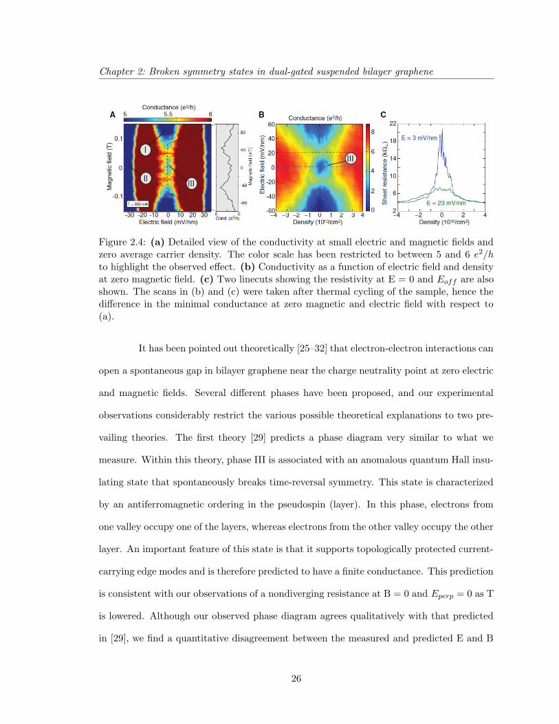
Figure 2.4: (a) Detailed view of the conductivity at small electric and magnetic fields andzero average carrier density. The color scale has been restricted to between 5 and 6 e2/hto highlight the observed effect. (b) Conductivity as a function of electric field and densityat zero magnetic field. (c) Two linecuts showing the resistivity at E = 0 and Eoff are alsoshown. The scans in (b) and (c) were taken after thermal cycling of the sample, hence thedifference in the minimal conductance at zero magnetic and electric field with respect to(a).
It has been pointed out theoretically [25–32] that electron-electron interactions can
open a spontaneous gap in bilayer graphene near the charge neutrality point at zero electric
and magnetic fields. Several different phases have been proposed, and our experimental
observations considerably restrict the various possible theoretical explanations to two pre-
vailing theories. The first theory [29] predicts a phase diagram very similar to what we
measure. Within this theory, phase III is associated with an anomalous quantum Hall insu-
lating state that spontaneously breaks time-reversal symmetry. This state is characterized
by an antiferromagnetic ordering in the pseudospin (layer). In this phase, electrons from
one valley occupy one of the layers, whereas electrons from the other valley occupy the other
layer. An important feature of this state is that it supports topologically protected current-
carrying edge modes and is therefore predicted to have a finite conductance. This prediction
is consistent with our observations of a nondiverging resistance at B = 0 and Eperp = 0 as T
is lowered. Although our observed phase diagram agrees qualitatively with that predicted
in [29], we find a quantitative disagreement between the measured and predicted E and B
26

Chapter 2: Broken symmetry states in dual-gated suspended bilayer graphene
transition values. We find that the magnetic field at which the spontaneous phase breaks
down is about 50 mT, an order of magnitude smaller than the theoretically predicted value
of 500 mT [29]. An applied electric field of about Eoff = 20 mV/nm quenches the spon-
taneous gap, compared to the predicted value of 26 mV/nm for the screened electric field.
Notably, we need to scale our measured Eoff by the screening constant k, which means that
our values differ by roughly a factor k = 3 from the theory [29]. A second prevailing theory
for the observed behavior stems from symmetry breaking, which results in the lowering of
the density of states at the charge neutrality point. One such example is the nematic state
that stems from the breaking of rotational symmetry due to electron-electron interactions.
This phase has been predicted to lead to a decreased density of states at the charge neu-
trality point due to the breaking of the system into two Dirac cones [31,32], consistent with
our measured decrease in conductance at small densities. Further experimental support for
the above two scenarios is given in [18], where it is shown that known single-particle effects
cannot explain the observed behavior.
2.7 Device fabrication
Substrate cleaning and graphene deposition are performed similar procedure to
that described by Feldman et al. [15]. Graphene bilayers are identified by their contrast
in an optical microscope and their characteristic quantum Hall effect. Suitable flakes are
contacted with Cr/Au contacts (3 nm/100 nm) by standard electron beam lithography,
thermal metal evaporation and lift-off in acetone. Silicon dioxide is structured on top of
graphene bilayers in a second electron beam lithography step, followed by electron beam
evaporation of silicon dioxide and lift off. The silicon dioxide is used as a spacer layer to
separate the top gate from the flake. A final electron beam lithography step is used to
27

Chapter 2: Broken symmetry states in dual-gated suspended bilayer graphene
pattern top gates that are suspended above the substrate in the areas that the silicon oxide
had been evaporated. Finally, the device is immersed into 5:1 buffered oxide etch for 90s
and dried in methanol in a critical point dryer.
28

Chapter 3
Gate defined quantum confinement
in suspended bilayer graphene
3.1 Overview
Quantum confined devices that manipulate single electrons in graphene are emerg-
ing as attractive candidates for nanoelectronics applications. Previous experiments have
employed etched graphene nanostructures, but edge and substrate disorder severely limit
device functionality. Here we present a technique that builds quantum confined structures
in suspended bilayer graphene with tunnel barriers defined by external electric fields that
open a bandgap, thereby eliminating both edge and substrate disorder. We report clean
quantum dot formation in two regimes: at zero magnetic field B using the energy gap in-
duced by a perpendicular electric field and at B > 0 using the quantum Hall ν = 0 gap
for confinement. Coulomb blockade oscillations exhibit periodicity consistent with electro-
static simulations based on local top gate geometry, a direct demonstration of local control
over the band structure of graphene. This technology integrates single electron transport
29

Chapter 3: Gate defined quantum confinement in suspended bilayer graphene
with high device quality and access to vibrational modes, enabling broad applications from
electromechanical sensors to quantum bits.
3.2 Quantum confinement in graphene
Nanopatterned graphene devices, from field-effect transistors to quantum dots [9,
41, 42], have been the subject of intensive research due to their novel electronic properties
and two-dimensional structure [1, 2]. For example, nanostructured carbon is a promising
candidate for spin-based quantum computation [43] due to the ability to suppress hyper-
fine coupling to nuclear spins, a dominant source of spin decoherence [44–46], by using
isotopically pure 12C. Graphene is a particularly attractive host for lateral quantum dots
since both valley and spin indices are available to encode information, a feature absent in
GaAs [47–49]. Yet graphene lacks an intrinsic bandgap [2], which poses a serious challenge
for the creation of such devices. Transport properties of on-substrate graphene nanos-
tructures defined by etching [9, 42] are severely limited by both edge disorder and charge
inhomogeneities arising from ionized impurities in gate dielectrics [50, 51]. The absence of
spin blockade in etched double dots is perhaps symptomatic of these obstacles [52,53]. Un-
zipping carbon nanotubes yields clean nanoribbon dots, but this approach cannot produce
arbitrarily shaped nanostructures with tunable constrictions [54]. However, local bandgap
engineering in bilayer graphene enables production of tunable tunnel barriers defined by
local electrostatic gates [55], thus providing clean electron confinement isolated from edge
disorder.
Bernal stacked bilayer graphene is naturally suited for bandgap control because of
its rich system of degeneracies that couple to externally applied fields. At B = 0, breaking
layer inversion symmetry opens an energy gap tunable up to 250 meV with an external
30

Chapter 3: Gate defined quantum confinement in suspended bilayer graphene
perpendicular electric field E [4,6,7,11,56–58] that can be used for confinement. In devices
with low disorder and at high magnetic fields, gapped states emerge from Coulomb-driven
effects that break its eightfold degeneracy (spin, valley, and orbital), resulting in quantum
Hall plateaus at all integer multiples of e2/h for electron charge e and Planck’s constant
h [59]. Due to the Pauli exclusion principle, Coulomb repulsions between electrons favor
spontaneous spin and/or valley polarization (or combinations of those), known as quantum
Hall ferromagnetism, resulting in a gap at zero carrier density that far exceeds the Zeeman
splitting energy gµBB [15,16]. The large exchange-enhanced energy gap of ∆ = 1.7 meV/T
measured for the ν = 0 state is ideally suited for quantum confinement [18]. Because valley
and layer indices are identical in the lowest Landau level, one may additionally induce a
tunable valley gap in the density of states by applying a perpendicular E field that breaks
layer inversion symmetry [60]. This coupling of valley index to E field is the key property
that enables direct experimental control of the relative spin and valley gap sizes in magnetic
field.
Here we demonstrate a technology that enables microscopic bandgap control in
graphene for the first time. We report fully suspended quantum dots in bilayer graphene
with smooth, tunable tunnel barriers defined by local electrostatic gating. Local gap control
in graphene opens an avenue to explore a variety of intriguing systems, including spin
qubits [43], topological confinement and valleytronics [61], quantum Hall edge modes in an
environment well-isolated from edge disorder, gate-controlled superconductivity, and many
more. While not the sole use for this technology, quantum dots provide a good experimental
platform to rigorously demonstrate local bandgap engineering due to the precise quantitative
relationship between dot area and quantized charge tunneling periodicity. Our technique,
which artificially modifies the bandgap of bilayer graphene over nanometer scales, achieves
clean electron confinement isolated from both edge and substrate disorder.
31

Chapter 3: Gate defined quantum confinement in suspended bilayer graphene
3.3 Device overview
We fabricate fully suspended quantum dots with 150 to 450 nm lithographic di-
ameters as illustrated schematically in Fig. 3.1a following the procedure described in the
Methods. Graphene is suspended between two Cr/Au electrodes and sits below suspended
local top gates (Fig. 3.1b and Supplementary Fig. A.1). Before measurement, the devices
are current annealed in vacuum to enhance quality. The high quality of our suspended
flakes is evident from the full lifting of the eightfold degeneracy in the quantum Hall regime
(Supplementary Fig. A.2) [60] and large resistances attained by opening the E field induced
gap at B = 0 and E = 90V/nm, a hundred times greater than reported for on-substrate
bilayers at similar electric fields [6, 60]. Measurements are conducted in a dilution refriger-
ator at an electron temperature of 110 mK, as determined from fits to Coulomb blockade
oscillations.
3.4 Quantum confinement at zero magnetic field
At B = 0, the electric field effect in bilayer graphene enables the production of
quantum confined structures with smooth, tunable tunnel barriers defined by local gat-
ing [47], thus avoiding disorder arising from the physical edge of the flake. Broken layer
inversion symmetry opens a bandgap ∆ ∝ E = (αVt − βVb)/2eε0, where Vt and Vb are top
and back gate voltages with coupling factors α and β, respectively, and ε0 is vacuum per-
mittivity. Coupling to the back gate β is extracted from Landau fans in the quantum Hall
regime and the relative gate coupling α/β can be determined from the Dirac peak slope in
a Vt vs. Vb plot of conductance at B = 0. Properties of individual quantum point contacts
are described in greater detail in Supplementary Figs. A.3 and A.4, where pinch-off and
behavior consistent with conductance quantization are observed. Quantum dot formation
32

Chapter 3: Gate defined quantum confinement in suspended bilayer graphene
Figure 3.1: (a) Schematic cross-section of a suspended gate-defined bilayer graphene quan-tum dot. The electric field and carrier density profiles are controlled with back and top gatevoltages Vb and Vt, while application of a bias Vsd across the electrodes enables transportmeasurements. (b) Scanning electron micrograph of quantum dot device similar to D4 (seeMethods for sample labeling key). Bilayer graphene (not visible) is suspended between twoelectrodes below local top gates. Green and blue lines indicate cross-sectional cuts in (a)and (c), respectively. Red lines mark the estimated graphene boundaries. The scale barrepresents 1µm. (c) Quantum dot formation at B = 0, illustrated in a cross-sectional cutof energy vs. position. EC and EV mark the edges of the conductance and valence bands.Tunnel barriers are formed by inducing a bandgap with an external E field while fixing Vt
and Vb at a ratio that places the Fermi energy EF within the gap. Uncompensated backgate voltage in the non top-gated regions enables charge accumulation in the dot and leads.
at B = 0 is illustrated schematically in Fig. 3.1c. To create tunnel barriers beneath the
top gates, we induce a bandgap by applying a field E while fixing Vt and Vb at a ratio
that maintains zero carrier density n, where n = αVt + βVb. In the non top-gated regions,
there is a finite charge accumulation due to an uncompensated back gate voltage. For gates
33

Chapter 3: Gate defined quantum confinement in suspended bilayer graphene
in a quantum dot geometry, this restricts electron transport to resonant tunneling events
through the constrictions.
Periodic Coulomb blockade oscillations are observed at B = 0 which couple to
both top and back gates (Fig. 3.2a). A peak in the 2D Fourier transform corresponding to
an oscillation spacing of ∼ 11mV in Vb reflects this strong periodicity (Fig. 3.2b), and the
appearance of higher harmonics reveals the non-sinusoidal nature of the Coulomb blockade
peaks when kBT EC, where kB is Boltzmann’s constant, T is temperature, and EC is the
dot charging energy. Coulomb diamonds shown in Fig. 3.2c have symmetric structure that
suggests equal tunnel coupling to both the source and drain leads. The dot charging energy
extracted from the DC bias data is EC ≈ 0.4 meV. Fig. 3.2d indicates that the periodic
Coulomb blockade oscillations have comparable capacitive coupling to each pair of top gates.
Furthermore, an even-odd effect is visible in a Coulomb blockade plot as a function of Vt12
at fixed Vt34 = 9.27 V and Vb = −10.7 V (Supplementary Fig. A.5), consistent with the
presence of a two-fold degeneracy. The conductance modulations that couple exclusively to
the back gate in Fig. 3.2a likely result from weak parallel conductance channels under gates
3 and 4 (as labeled in Fig. 3.1b) and are unrelated to the central gate-defined quantum dot
formation because capacitive coupling to Vt12 is absent. The horizontal modulations in Fig.
3.2d couple only to Vt34 but not Vt12 and are thus expected to have similar origins. Because
these features are sparse and aperiodic in nature, we expect that they are not generated
by random dot formation in the constrictions or under the local gates. We note that the
highly resistive ν = 0 gap in the quantum Hall regime enables more robust confinement
than the electric field induced gap, and we demonstrate that all background conductance
fluctuations are completely eliminated in Fig. 3.3.
34

Chapter 3: Gate defined quantum confinement in suspended bilayer graphene
Figure 3.2: (a) Conductance map (units of e2/h) of Coulomb blockade oscillations as afunction of back gate voltage (Vb) and the voltage on top gates 1 and 2 (Vt12) at T = 110mK in a four gate dot (device D4). The voltage on top gates 3 and 4 is fixed at Vt34 = 9.27V. (b) 2D fast Fourier transform (units of e2/h · V ) of (a) reveals the periodic structure.A peak corresponding to an oscillation spacing of ∼ 11mV in Vb reflects strong periodicity,while the appearance of higher harmonics reveals the non-sinusoidal nature of the Coulombblockade peaks when kBT EC. (c) Coulomb diamonds are shown in a plot of ∆G/∆Vt12asa function of Vt12 and VDC, where G is conductance in units of e2/h and VDC is the DCbias across the electrodes. The voltages Vb = −10.7V and Vt34 = 9.27 V are held constant.Symmetric Coulomb diamonds suggests equal tunnel coupling to source and drain leads.The dot charging energy is EC ≈ 0.4 meV. (d) Conductance map (units of e2/h) of Coulombblockade oscillations as a function of Vt12 and Vt34 at fixed back gate voltage Vb = −10.7V.
3.5 Coulomb blockade in the quantum Hall regime
Coulomb blockade oscillations can also be generated at finite B field using the
exchange-enhanced ν = 0 gap. Here the bilayer is naturally in a gapped quantum Hall
state at zero density, where high resistances due to quantum Hall ferromagnetism make this
system ideal for confinement. An isolated puddle of charge is created by fixing the Fermi
energy in the top-gated regions at the middle of the ν = 0 gap while allowing occupation
of higher Landau levels elsewhere, shown schematically in Fig. 3.3a. It should be noted
that measurements in the quantum Hall regime are conducted in the valley-polarized ν = 0
state, far from the transition to the spin-polarized phase [60]. Fig. 3.3b shows over forty
consecutive Coulomb blockade oscillations generated at 5.2 T in a 2-gate dot with a 400
35

Chapter 3: Gate defined quantum confinement in suspended bilayer graphene
nm lithographic diameter. The slopes of the resonances indicate symmetric coupling to
the two top gates, as expected for a centrally located dot. As top gate voltages are swept
to more positive values, peak amplitude is suppressed, revealing moderate tunnel barrier
tunability. Also seen in Fig. 3.3b are interruptions in the conductance resonances (vertical
and horizontal features) that couple exclusively to a single top gate; due to their sparse and
aperiodic nature, we believe that they represent charging events below the gates. Coulomb
blockade oscillations are robust over a wide voltage range: Fig. 3.3c shows an additional
forty peaks generated under new gate conditions. The Coulomb diamonds exhibit symmetric
tunnel coupling to source and drain leads and a dot charging energy of EC ≈ 0.4 meV. The
strongly periodic nature of the oscillations is evident in the Fourier transform of the data
(Fig. 3.3d). See Supplementary Fig. A.6 for additional Coulomb blockade data.
3.6 Geometric control over Coulomb blockade period
To demonstrate geometric control over dot size, we examine the correspondence
between top gate dimensions and Coulomb blockade peak spacing. Measurements were
performed on five dots with lithographic diameters ranging from 150-450 nm at magnetic
fields of 0 to 7 T. The ability to decrease peak spacing by increasing lithographic dot size is
illustrated in Fig. 3.4a-c. Fig. 3.4a and 3.4b show Coulomb blockade peak conductance as
a function of back gate voltage Vb observed in device D1 at B = 5.2 T, and D2 at B = 7 T,
respectively (see Methods for sample labeling key). Black points represent data and the red
lines are fits used to extract peak positions. Fig. 3.4c shows relative peak position, V (p)−V0,
plotted as a function of peak number p for the first 10 peaks of Fig. 3.4a and 3.4b, where V (p)
is the position of peak p in back gate voltage, and V0 is the position of the first peak. Each
data set is accompanied by a corresponding plot of y(p) = [19
∑8q=0 V (q+1)−V (q)]p, where
36

Chapter 3: Gate defined quantum confinement in suspended bilayer graphene
Figure 3.3: (a) Quantum dot formation at B > 0, illustrated in a cross-sectional cut ofenergy vs. position. Tunnel barriers are formed using the exchange-enhanced ν = 0 gap,where high resistances due to quantum Hall ferromagnetism are ideal for confinement. Anisolated puddle of charge is created by fixing the Fermi energy in the top-gated regions atthe middle of the ν = 0 gap while allowing occupation of higher Landau levels elsewhere.Inset : Schematic illustration of the top gate geometry for device D1. (b) Conductancemap (units of e2/h) of Coulomb blockade oscillations as a function of Vt1 and Vt2 in atwo top-gate dot (device D1), at fixed back gate voltage Vb = −15.4V and T = 110 mK.The slopes of the resonances indicate symmetric coupling to the two top gates, as expectedfor a centrally located dot. As top gate voltages are swept to more positive values, peakamplitude is suppressed, revealing moderate tunnel barrier tunability. Inset : Scanningelectron micrograph of a device similar to D1. (c) Coulomb diamonds are shown in a plotof conductance (units of e2/h) as a function of Vt1 and DC bias VDC, where Vt2 = 11 Vand Vb = −14.4 V are fixed. Symmetric Coulomb diamonds suggests equal tunnel couplingto source and drain leads. The dot charging energy is EC ≈ 0.4 meV. (d) 2D fast Fouriertransform (units of e2/h · V ) of the boxed region in (b), revealing the strongly periodicnature of the oscillations and higher harmonics.
p and q are peak index numbers, representing the average peak spacing (black lines in Fig.
3.4c). The dot area extracted from quantized charge tunneling is given by A = 1/(β ·∆Vb),
where ∆Vb is the back gate voltage needed to increase dot occupation by one electron (Table
3.1). A comparison of measured dot diameter, d = 2√A/π, with effective lithographic
37

Chapter 3: Gate defined quantum confinement in suspended bilayer graphene
diameter, dlith = 2√Alith/π, indicates that d generally exceeds dlith. This is contrary to the
reduced dimensions observed in GaAs dots, where smaller dimensions are observed due to
depletion [62].
Figure 3.4: (a) Coulomb blockade peak conductance as a function of back gate voltageVb observed in device D1 at B = 5.2 T. Black points represent data and the red lineindicates a functional fit used to extract peak positions. The top gate voltages are fixedat Vt1 = 11.402 V and Vt2 = 12 V.(b) Coulomb blockade in device D2 at B = 7 T. Thetop gate voltages are fixed at Vt1 = Vt3 = 13 V and Vt2 = Vt4 = 12 V. (c) Relative peakposition, V (p)−V0, plotted as a function of peak number p for the first 10 peaks of (a) and(b). V (p) is the position of peak p in back gate voltage Vb, and V0 is the position of the firstpeak (V0 = −15.4907 V and −17.9875 V for plots (a) and (b), respectively). Each blackline is a plot of y(p) = [1
9
∑8q=0 V (q + 1)− V (q)]p, where p and q are peak index numbers,
representing the average peak spacing for the particular data set. Inset : Simulated dot sizeversus measured size. Error bars represent the range of diameters expected for measuredCoulomb blockade peak spacings within one standard deviation of the mean. (d) COMSOLsimulation of density profile (in arbitrary units) for the lithographic gate pattern of deviceD4 for top gate voltage Vt1 = Vt2 = 12 V. Electron transport is restricted to resonanttunneling events through the constrictions, indicated by the arrows.
To obtain a better quantitative understanding of the discrepancy between litho-
graphic and measured dot sizes, we use a commercial finite element analysis simulation tool
(COMSOL) to calculate the expected dot area for each top gate geometry. The spatial
38

Chapter 3: Gate defined quantum confinement in suspended bilayer graphene
Table 3.1: Measured quantum dot sizes from Coulomb blockade fits
Device β, m−2V −1 〈∆Vb〉, mV St. deviation of ∆Vb Diameter, d = 2√A/π
D1 2.85× 10¹⁴ 14.0 1.8 565(+40/− 34) nmD2 3.19× 10¹⁴ 34.1 5.3 342(+30/− 24) nmD3 3.05× 10¹⁴ 68.8 4.2 260(±8) nmD4 2.71× 10¹⁴ 10.7 1.7 663(+60/− 47) nmD5 2.85× 10¹⁴ 13.7 1.3 571(+29/− 26) nm
β: density at 1 V on the back gate. 〈∆Vb〉: average peak spacing. Dot diameter: d = 2√A/π
for area A = 1/(β ·∆Vb). Error bars in the last column: range of diameters for CB peakspacings within one standard deviation of the mean. See Fig. 3.4a.
carrier density profile is modeled for a fixed top gate potential by solving the Poisson equa-
tion assuming a metallic flake in free space (Fig. 3.4d and Supplementary Fig. A.7). This
assumption is justified by local compressibility measurements of the ν = 0 state yielding
dµ/dn = 2 × 10⁻¹⁷eV m2 at 2 T, which translates to a screening of 99% of the applied Vb
voltage by the bilayer [18]. Remarkably, one may calculate dot size purely from gate geom-
etry without relying on measured gap parameters. Assuming that charge accumulation in
the quantum dot occurs when the carrier density exceeds a fixed cutoff d0, the dot size is
defined as the area bounded by the intersection with the density distribution f(x, y) with
the cutoff. Here the cutoff d0 is placed at the saddle points of the simulated density profile
within the constrictions. This condition enables maximal tunneling without loss of con-
finement, assuming that the tunneling probability into the dot decays exponentially with
barrier width. Moving the cutoff to densities far greater than d0 would pinch off the con-
strictions and suppress tunneling, while placement far below d0 would lead to high barrier
transparency and eventual loss of confinement. The simulated dot area from this method,
plotted in Fig. 3.4c (inset), is simply the area bounded by the closed contour of f(x, y) at
fixed density d0 (Supplementary Fig. A.7). Alternatively, one may calculate dot size by
imposing a cutoff equaling the measured gap width (Table 3.2) and accounting for density
39

Chapter 3: Gate defined quantum confinement in suspended bilayer graphene
offsets due to a displacement of the measurement voltage from the charge neutrality point
(see Extended Discussion). The cutoffs extracted by these two models are equivalent to
within δn ∼ 1010cm−2, the carrier density fluctuations due to disorder in our suspended
bilayers (Supplementary Fig. A.7) [15].
Table 3.2: Simulated dot sizes obtained from Models 1 and 2
Device d0, m−2 d1, m−2 Diameter (Model 1) Diameter (Model 2)
D1 7.87× 10¹⁴ 6.81× 10¹⁴ 489 nm 564 nmD2 1.85× 10¹⁴ 1.45× 10¹⁴ 170 nm 204 nmD3 7.59× 10¹⁴ 8.34× 10¹⁴ 340 nm 300 nmD4 4.29× 10¹⁴ 3.90× 10¹⁴ 504 nm 537 nmD5 6.96× 10¹⁴ 6.59× 10¹⁴ 533 nm 562 nm
Densities d0 and d1: cutoff values above which charge accumulation begins in Models 1and 2. Dot diameter: d = 2
√A/π for area A. Diameters from Model 2 were computed at
maximum offset doffset = (Vmeas − VCNP )β. See Fig. A.7.
Our model establishes a quantitative link between measured dot size and litho-
graphic geometry and therefore may serve as a design tool for future bilayer nanodevices
requiring submicron spatial control. These include double dot systems which form the basis
of a spin-based quantum computer [43]. The production of suspended graphene quantum
dots also enables study of coupling between quantized electronic and vibrational degrees
of freedom [63, 64], with potential applications to nanoelectromechanical devices and the
detection of quantized mechanical motion in a membrane [65–68]. Furthermore, the com-
bination of high sample quality with local gating enables study of edge modes that emerge
at the interface of broken symmetry quantum Hall states in an environment well-isolated
from edge disorder (Supplementary Fig. A.2).
40

Chapter 3: Gate defined quantum confinement in suspended bilayer graphene
3.7 Methods
Device fabrication
Following mechanical exfoliation of highly oriented pyrolytic graphite crystals,
graphene is deposited on a 300 nm thermally grown SiO2 layer, which covers a doped silicon
substrate functioning as a global back gate. Bilayer flakes are identified based on contrast
to the substrate with an optical microscope and later verified through quantum Hall data.
Cr/Au (3/100 nm) electrodes are defined on selected bilayers using electron beam (ebeam)
lithography, thermal evaporation, and liftoff in acetone. A SiO2 spacer layer approximately
150 nm thick is deposited with ebeam evaporation after a second lithography step. Local
top gates are placed over the SiO2 spacers in a two step ebeam lithography process. First
small features that define the tunnel barriers and constrictions are patterned using Cr/Au
of thickness 3/75 nm, and thicker support structures constructed of 3/300 nm of Cr/Au
that traverse the evaporated SiO2 step are deposited immediately afterwards. The devices
are immersed in 5:1 buffered oxide etch for 90 s and dried in a critical point dryer, which
leaves both the graphene and the top gates suspended.
Dot geometries and measurement conditions
We analyze five fully suspended quantum dots with lithographic diameters, dlith =
2√Alith/π, of 150 to 450 nm. Listed here are details on individual sample geometries
and measurement conditions. Device D1 is a circular two gate dot with dlith = 400 nm
measured at B = 5.2 T with the valley polarized ν = 0 gap used for confinement. Device
D2 is a circular dot with dlith =150 nm consisting of three main gates with a plunger gate
suspended above (see Supplementary Figure A.1). Measurements were conducted at B = 0
and 7 T with the E field induced and ν = 0 gaps used for confinement, respectively. Device
41

Chapter 3: Gate defined quantum confinement in suspended bilayer graphene
D3 is a circular four gate dot with dlith = 300 nm measured at B = 7 T. Device D4 is a
circular four gate dot with dlith = 400 nm measured at B = 0 and 3 T. Device D5 is a
two gate elliptical dot with cross sectional lengths of 200 and 250 nm measured at B = 5
T. Additional scanning electron microscope (SEM) images of locally gated quantum dot
devices are provided in Supplementary Fig. A.1. Top gate labeling for devices D2 and D4
is provided in Supplementary Fig. A.1 and Fig. 3.1, respectively. All measurements are
conducted using standard Lockin techniques in a Leiden Cryogenics Model Minikelvin 126-
TOF dilution refrigerator. A voltage bias setup is used, where AC excitations ranging from
4− 80µV are applied at a frequency of 35.35 Hz with a 100 ms time constant. An electron
temperature of T = 110 mK is extracted from Coulomb blockade fits.
Despite the complex fabrication process required to make local gated devices, the
graphene exhibits high quality as evidenced by symmetry breaking in the quantum Hall
regime. Supplementary Fig. A.2 contains Landau fans (measured in device D4 and in
a two gate split-gate device) plotted as conductance as a function of back gate voltage
Vb and magnetic field B, with zero voltage on the top gates. In the split gate device,
a map of quantized conductance as a function of the voltages on each split top gate is
provided in Supplementary Fig. A.2, where the voltage Vb = −3V and field B = 4T are
held constant. This provides evidence of local control over broken symmetry quantum Hall
states in suspended bilayer graphene.
Measured dot size extracted from Coulomb blockade fits
The dot area extracted from quantized charge tunneling is given by A = 1/(β ·
∆Vb), where ∆Vb is the back gate voltage needed to increase dot occupation by one electron
and β is the carrier density induced by 1 V on the back gate. The global density to voltage
conversion is obtained by fitting Landau level filling factors ν = nh/eB from bulk quantum
42

Chapter 3: Gate defined quantum confinement in suspended bilayer graphene
Hall data. The peak spacing ∆Vb ≡ V i+1b,res− V
ib,res of a given data set is extracted by fitting
each Coulomb blockade oscillation to the conductance expression:
G(Vb) = A · cosh
(ea|Vb − Vb,res|
2.5kBT
)−2
(3.1)
where e is the electron charge, kB is Boltzmann’s constant, T is temperature, A is peak
amplitude, Vb,res, is the back gate voltage at resonance, and a = Cg/(Cl + Cr + Cg) is
determined from the slopes of the Coulomb diamonds (Cg is capacitance to the back gate
and Cl and Cr are capacitances across the left and right tunnel barriers, respectively). This
expression is valid in the regime ∆E kBT e2/C, where ∆E is the single particle level
spacing. This functional fit to the data is shown explicitly in Fig. 3.4a,b. Coulomb blockade
data from an additional device is provided in Supplementary Figure A.4.
3.8 Extended Discussion
Even-odd effects
At zero magnetic field, the presence of a four-fold degeneracy due to spin and
valley symmetries may affect the Coulomb blockade periodicity (at high electric fields in
the quantum Hall regime, both spin and valley degeneracies should be broken). In device
D4, an even-odd effect is visible in a Coulomb blockade plot as a function of Vt12 at fixed
Vt34 = 9.27V and Vb = −10.7V (Supplementary Fig. A.5). This is consistent with the
presence of a two-fold degeneracy, where the constant interaction model yields electron
addition energy Eadd = EC for N odd and Eadd = EC+∆E for N even (for charging energy
EC and orbital energy spacing ∆E) because electrons of opposite index can occupy a single
orbital state [40, 41]. Although the application of a large electric field breaks sublattice
symmetry, spin and valley degeneracies remain intact, so an explanation of our observation
43

Chapter 3: Gate defined quantum confinement in suspended bilayer graphene
of a two-fold rather than four-fold effect remains an open question. Also, the theoretical
estimate of ∆E based on device geometry is larger than the measured value; this discrepancy
cannot be explained by a single particle picture and requires further investigation.
Model 1: Cutoff defined by constriction saddle points
We first discuss simulation of the spatial density profile for each quantum dot, as
shown in Fig. 3.4d, which is relevant to the final two sections of the Extended Discussion.
COMSOL Multiphysics, a commercial finite element analysis simulation tool, is used to
model the spatial carrier density profile for a fixed top gate potential by solving the Poisson
equation, ∇2V = −ρ/ε0. First the lithographic top gate pattern, designed using TurboCAD,
is imported into COMSOL and placed in a parallel plane defined 150 nm above the graphene
flake. The flake is assumed to be a two dimensional metallic plate, which is justified by
local compressibility measurements of the ν = 0 state yielding dµ/dn = 2 × 10⁻¹⁷eV m2
at 2 T, which translates to a screening of 99% of the applied Vb voltage by the bilayer
(for dn = 1.5 × 109 cm−2) [42]. A fixed potential matching the experimental value at
which Coulomb blockade oscillations appear is assigned to the top gates, while the flake
is grounded. The perpendicular electric field component, Ez(x, y), is solved in a plane
5 nm above the flake. The approximate carrier density profile is given by the function
f(x, y) = e · Ez(x, y)/ε0 up to a constant offset. This is because the graphene screens all
in-plane electric fields. A contour plot representing the simulated spatial density profile in
device D4 at a top gate voltage of 12 V is presented in Supplementary Figure A.7.
In the first modeling approach, whose results are presented in Fig. 3.4c, one may
calculate dot size purely from gate geometry without relying on measured gap parameters.
Assuming that charge accumulation in the quantum dot occurs when the carrier density
exceeds a fixed cutoff d0, the dot size is defined as the area bounded by the intersection with
44

Chapter 3: Gate defined quantum confinement in suspended bilayer graphene
the density distribution f(x, y) with the cutoff. Here the cutoff d0 is placed at the saddle
points of the simulated density profile within the constrictions. This condition enables
maximal tunneling without loss of confinement, assuming that the tunneling probability into
the dot decays exponentially with barrier width. Thus, the simulated dot area computed
by this method is simply the area bounded by the closed contour of f(x, y) at fixed density
d0 (Supplementary Fig. A.7a).
The model is used to estimate the extent to which dot size should change in
response to a changing top gate voltage. The dot diameter, d = 2√A/π, for sample D2 is
computed to be 170 nm at top gate voltage Vt = 9 V and 173.5 nm at Vt = 13V. This 3.5
nm increase in diameter, a 2 percent change, over a 4 V range is substantially smaller than
the experimental error bars due to fluctuations in peak spacing (Fig. 3.4). This prediction
is consistent with the overall experimental observation of an approximately constant dot
size over the measurement ranges presented in this paper.
Model 2: Cutoff determined from measured ν = 0 gap and offset from charge
neutrality point
In the second modeling approach, we determine quantum dot dimensions using
both the simulated density distribution and experimental gap measurements. First the
spatial density profile induced by the top gates, f(x, y), is modeled using COMSOL following
the procedure described in the preceding section of the Extended Discussion. To determine
the quantum dot size from the density profile, we impose a cutoff d1 determined by the
width of the gap (ν = 0 or E field induced) above which charge accumulation begins.
Explicitly, d1 = (V+ − V−)β, where V+ and V− are the positive and negative back gate
voltages at which a plot of conductance versus Vb intersects 1e2/h. Additionally we account
for overall offsets in density due to a displacement of the measurement voltage from the
45

Chapter 3: Gate defined quantum confinement in suspended bilayer graphene
charge neutrality point. This offset is given by doffset = (Vmeas − VCNP )β, where Vmeas is
the measured back gate voltage at which Coulomb blockade oscillations appear, and VCNP
is the measured back gate voltage at which the charge neutrality point appears at B = 0
when the top gates are fixed at the potential defined in the density profile simulation. Thus,
the spatial density profile with proper offsets included is g(x, y) = f(x, y) − dsat + doffset,
where dsat is the saturating value of f(x, y) deep within the tunnel barriers defined by the
top gates. Physically dsat is the offset in carrier density induced by the back gate that
places the Fermi energy at the center of the bandgap. Similar to Model 1, the simulated
dot area computed by this method is the area bounded by the contour lines of g(x, y) at
fixed density d1. Results of Models 1 and 2 are presented in Table 3.2 and Supplementary
Figure A.7.
46

Chapter 4
Spatially resolved edge currents in
monolayer and bilayer graphene
4.1 Overview
Extreme nonclassical forms of electronic transport realized in graphene by exploit-
ing the light-like properties of carriers in this material are of keen interest for nanoscience
research [69–76]. In this vein, finding ways to confine and direct electronic waves through
nanoscale streams and streamlets, unimpeded by the presence of other carriers, has remained
a grand challenge [77–80]. Inspired by guiding of light in fiber optics, here we demonstrate
a route to engineer such a flow of electrons using a new technique for mapping currents
at submicron scales. We employ real-space imaging of current flow in graphene to provide
direct evidence of confinement of electron waves at the edges of a graphene crystal near
charge neutrality. This is achieved by using superconducting interferometry in a graphene
Josephson junction and reconstructing the spatial structure of conducting pathways using
Fourier methods [24]. The observed edge currents arise from coherent guided wave states,
47

Chapter 4: Spatially resolved edge currents in monolayer and bilayer graphene
confined to the edge by band bending and transmitted as plane waves. As an electronic
analog of photon guiding in optical fibers, the observed states afford new nonclassical means
for information transduction and processing at the nanoscale.
4.2 Guided-wave electronic states in graphene
Electrons in Dirac materials such as graphene can be manipulated using external
fields that control electron refraction and transmission in the same way that lenses and
optical elements manipulate light [69, 70, 74, 75]. Several of the key ingredients, including
phase-coherent Klein transmission and reflection [71–73], ballistic transport [76] and trans-
verse focusing on micrometer scales [81], have already been established. One promising yet
unexplored direction, which we investigate here, is the quasi-1D confinement of electrons
in direct analogy to refraction-based confinement of photons in optical fibers. Electronic
guided modes formed by a line gate potential, while discussed in the literature [77–80], have
so far evaded direct experimental realization. Extending the fiber optics techniques to the
electronic domain is key for achieving control of electron waves at a level comparable to
that for light in optical communication systems.
Rather than pursuing the schemes discussed in Refs. [77–80], here we explore
modes at the graphene edges. The atomically sharp graphene edges provide a natural
vehicle for band bending near the boundary which then confines the electronic waves in
the direction transverse to the edge. The resulting guided “fiber-optic” modes are situated
outside the Dirac continuum (see Fig. 4.1a,b), propagating along crystal edge as plane
waves and decaying into the bulk as evanescent waves. This approach to carrier guiding is
particularly appealing because of the ease with which band bending at the graphene edge
can be realized, as well as because there is no threshold for fiber-optic states to occur:
48

Chapter 4: Spatially resolved edge currents in monolayer and bilayer graphene
they are induced by an edge potential of either sign, positive or negative, no matter how
weak (see discussion below and in the Extended Discussion). The presence of such guided
modes enhances the density of current-carrying states at the edge. The effects of electron
confinement and guiding are strongest near charge neutrality where the edge potential is
unscreened, while uniform behavior is recovered away from neutrality (see Fig. 4.1c and
Fig. 4.5).
The edge currents associated with guided states, anticipated at zero magnetic field,
have so far eluded experimental detection due to the challenge of imaging current with sub-
micron spatial resolution. In particular, scanning tunneling spectroscopy (STS) images den-
sity of states but not current flow [82,83], while macroscopic conductivity cannot distinguish
the edge and bulk contributions [84, 85]. With this motivation, we developed a technique
to spatially image electric current pathways and applied it to high-mobility graphene. We
employ superconducting quantum interferometry in a graphene Josephson junction to re-
construct the spatial structure of the electronic states which transmit supercurrent, which
allows edge and bulk contributions to be disentangled [24,86].
4.3 Experiment: spatial imaging of current flow using Joseph-
son interferometry
Our approach employs gated Josephson junctions consisting of graphene coupled
to superconducting titanium/aluminum electrodes (Fig. 4.1d). A gate electrode is used
to tune the carrier density, n, in the graphene. In order to access the intrinsic properties
of graphene at densities near charge neutrality, flakes are isolated from substrate-induced
disorder through placement on thin hexagonal boron nitride (hBN) substrates [87]. A total
of four bilayer and one monolayer devices are investigated, all of which exhibit similar
49

Chapter 4: Spatially resolved edge currents in monolayer and bilayer graphene
behavior (Table 4.1). Measurements of the AC voltage drop dV across the junction in
response to an AC current modulation dI were conducted using lockin techniques in a
dilution refrigerator at 10 mK, well below the critical temperature of Al. Figures 4.1e-h
exemplify transport data from one of the bilayer devices. Upon sweeping DC current bias
IDC , a sharp transition in resistance between dissipationless and normal metal behavior
appears at a critical current Ic, a transport signature of the Josephson effect (Fig. 4.1e,f).
Table 4.1: List of device dimensions for graphene Josephson junctions
Device L (nm) W (nm) Aspect ratio, L/W Contact width (nm)
BL1 250 1200 0.208 400ML1 300 1200 0.25 300BL2 300 800 0.375 400BL3 350 1200 0.292 600BL4 250 900 0.278 400
L and W refer to junction length and width, respectively, as labeled in Fig. 4.1d of themain text. Contact width refers to the size of the superconducting Ti/Al electrodes inthe direction perpendicular to W. BLx and MLx refer to bilayer and monolayer graphenedevices, respectively.
We obtain real-space information by applying a magnetic flux Φ through the junc-
tion area, which induces a position-dependent superconducting phase difference parallel to
the graphene/contact interface [23]. As a result, the critical current Ic exhibits interference
fringes in B field (Figure 4.1e). The measured interference patterns feature well defined
nodes, which indicates the absence of field inhomogeneity such as that due to vortices [88].
The critical current Ic can be expressed as the magnitude of the complex Fourier transform
of the current density distribution J(x), providing a simple and concise description of our
system. That is, Ic = |Ic(B)|, where
Ic(B) =
∫ W/2
−W/2J(x) · e2πiLBx/Φ0dx (4.1)
50

Chapter 4: Spatially resolved edge currents in monolayer and bilayer graphene
where Φ0 = h/2e is the flux quantum, h is Planck’s constant, e is the elementary charge, W
is the width of the flake, and L is the distance between contacts (Fig. 4.1d). Here, following
the conventional treatment for wide junctions (LW ), we ignore the y dependence. The
spatial distribution of supercurrent thus dictates the shape of the interference pattern [23,
24,49].
The results obtained with this technique show strikingly different behavior at
high and low carrier densities. We observe the conventional uniform-current behavior at
high density, Ic(B)/Ic(0) ∼ | sin(πΦ/Φ0)/(πΦ/Φ0)|, which mimics single-slit Fraunhofer
diffraction (Fig. 4.1e). Defining features of such interference include a central lobe of
width 2Φ0 and side lobes with period Φ0 and decaying 1/B amplitude. However, near the
Dirac point, our results exhibit a striking departure from this picture and show a two-slit
“SQUID-like” interference (Fig. 4.1f) [89]. Such behavior arises when supercurrent is
confined to edge channels and is characterized by slowly decaying sinusoidal oscillations of
period Φ0. Importantly, these two regimes are easily distinguishable without much analysis
by the width of the central lobe, which is twice as wide for the uniform case as compared
to the case of edge flow.
The real-space current distribution can be obtained by inverting the relation in
Eq.(1) with the help of the Fourier techniques of Dynes and Fulton [24] (see Extended Dis-
cussion). The resulting current density map reveals strong confinement of supercurrent to
the edges of the crystal near the Dirac point (Fig. 4.1h), a robust experimental feature seen
in all five devices. The width of the edge channel, extracted quantitatively from Gaussian
fits, is on the order of the electron wavelength (∼ 200 nm) and consistent across multiple
samples. This value is likely an upper bound because the peak width is manifested in the
decay envelope of the interference pattern, external factors that suppress the critical current
amplitude at high B, such as activation and decay of the Al superconducting gap, may also
51

Chapter 4: Spatially resolved edge currents in monolayer and bilayer graphene
contribute to peak broadening. At high electron density, a conventional Fraunhofer-like
behavior is recovered (Fig. 4.1e), suggesting a uniform distribution of supercurrent (Fig.
4.1g). A more numerically expensive Bayesian estimation of the current distribution pro-
duces current maps and standard error estimates that agree with the Fourier techniques
(see Extended Discussion and Fig.4.6 within).
By tuning carrier concentration with a gate electrode, our measurements reveal
coexistance of edge and bulk modes at intermediate densities. As illustrated in Fig.4.2,
our monolayer graphene device exhibits SQUID-like quantum interference through charge
neutrality, giving the spatial image of supercurrent that confirms edge-dominated transport
(Fig. 4.2a-c,f). As density is increased, bulk current flow increases monotonically and
crosses over to mostly uniform flow across the sample (Fig. 4.2d), signified by conventional
Fraunhofer-like interference at high electron density (Fig. 4.2e). To track the evolution of
edge and bulk currents with density, line cuts of the individual contributions are provided in
Figure 4.2e, where the gate voltage corresponding to the charge neutrality point is identified
as a dip in the current amplitude. Notably, raw interference near the Dirac point (Fig. 4.2e)
and at high electron concentration (Fig. 4.2f) exhibit the salient features that distinguish
edge-dominated from bulk-dominated transport, including a width of ϕ0 versus 2ϕ0 of the
central lobe, as well as Gaussian versus 1/B decay of the lobe amplitudes for low and high
densities, respectively.
Similarly, we systematically explore the correspondence between edge and bulk
flow in bilayer graphene and detect boundary currents in the presence of broken crystal
inversion symmetry (Fig. 4.3). As the Fermi energy approaches the Dirac point from
the hole side, the bulk is suppressed faster than the edge, leading to emergence of robust
52

Chapter 4: Spatially resolved edge currents in monolayer and bilayer graphene
Figure 4.1: (a, b) Guided edge modes induced by an intrinsic band bending near crystalboundary, for single-layer and bilayer graphene (schematic). Mode frequencies positionedoutside the Dirac continuum ensure mode decoupling from the bulk states. In a bilayer,the modes occur in pairs [green and red curves : dispersion for positive and negative po-tential strength, respectively]. (c) The guided modes are manifested through peaks in thedensity of current-carrying states at the boundaries, prominent near charge neutrality (red :n = 0.05 × 1011cm−2; blue: n = 2.5 × 1011cm−2). (d) Schematics of superconductinginterferometry in a graphene Josephson junction. A flux is threaded through the junctionarea to produce interference patterns, as current bias Vsd is applied between the contactsand the voltage across the device is recorded. Carrier density n is tuned by a gate voltageVb. (e, f) The interference pattern is of a single-slit type at high density, turning intoa two-slit interference near neutrality (device BL1). (g, h) Current flow, extracted fromthe interference data using Fourier techniques, is uniform at high density and peaks at theedges close to neutrality.
edge currents near zero carrier density (Fig. 4.3a,b). In this device, current distributions
are not plotted at the immediate Dirac point due to suppression of proximity-induced
superconductivity at high normal state resistances. We note that the range in hole density
53

Chapter 4: Spatially resolved edge currents in monolayer and bilayer graphene
over which the bulk contribution is recovered varies in different devices. Further, application
of an interlayer electric field E breaks crystal inversion symmetry and induces a bandgap [3,
90], manifested as a gate-tunable insulating state at the Dirac point (Fig. 4.3c,d). In this
regime, conductance is mediated by edge currents that enclose the bulk, even in the presence
of a gap (Fig. 4.3e,f).
Figure 4.2: (a) Edge-dominated SQUID-like interference pattern at neutrality in deviceML1 (n = 2.38 × 109 cm−2). (b, c) Real-space image of current flow confined to theboundaries over a range of densities near neutrality, shown alongside with the raw interfer-ence data (corresponding to the white box in (d)). (d) A real-space map of current flowas a function of electron concentration reveals coexistence of edge and bulk modes at inter-mediate densities. Over the entire scan, the full range of carrier modulation extends intothe high 1011 range cm−2. (e) Conventional Fraunhofer pattern for uniform current flow athigh electron density (n = 7× 1011 cm−2). (f) Comparison of current amplitudes along theedge (red) and bulk (blue) from panel (c). Current flow is edge-dominated near neutrality.Minima for both contributions coincide in n, indicating that a positional edge/bulk densityoffset is not present.
54

Chapter 4: Spatially resolved edge currents in monolayer and bilayer graphene
Figure 4.3: (a) Spatially resolved supercurrent map in device BL2, in a normalized plot ofJ(x)/Jmax(x). Edge-dominated transport occurs near charge neutrality, while an increasingbulk contribution is tuned with carrier concentration. (b) Comparison of current amplitudesalong the edge (red) and through the bulk (blue) from panel (a). Enhanced edge currents areprominent at neutrality, whereas a uniformly distributed flow is recovered at high densities.The normal state conductance G(e2/h) vs. carrier density is also shown (black). (c)Measurement schematic for superconducting interferometry in a dual-gated bilayer grapheneJosephson junction. A dual-gated device consists of bilayer graphene flake on hBN witha suspended top gate, where application of voltages Vt and Vb on the top and back gatesenables independent control of the transverse electric field E and carrier density n. (d)Resistance map as a function of Vb and Vt for bilayer BL4. Enhanced resistance at highE fields indicates the emergence of a gate-tunable insulating state due to broken crystalinversion symmetry. (e) Spatially-resolved boundary currents as a function of E field.The vertical axis is a trace along the red path labeled in (b). (f) Sequence of Fraunhofermeasurements at various locations on the current map in panel (e).
55

Chapter 4: Spatially resolved edge currents in monolayer and bilayer graphene
As a simple model of electronic fiber-optic states we consider massless Dirac par-
ticles in graphene monolayer in the presence of a line potential:
H = vσ · p+ V (x), (4.2)
where σi are pseudospin Pauli matrices and v ≈ 106 m/s. We seek plane-wave solutions of
the Schrodinger equation, ψ(x, y) = eikyϕ(x), where k is the wavevector component along
the line and ϕ(x) is a two-component spinor wavefunction depending on the transverse co-
ordinate. This problem can be tackled by a matrix gauge transformation ψ(x) = U(x)ψ(x),
which eliminates the potential V (x) and generates a mass term in the Dirac equation.
Namely, U(x) = e−iθ(x)σx with θ(x) = 1~v∫ x
0 V (x′)dx′ yields
H = U(x)HU−1(x) = ~v[−iσx∂x + kσy cos 2θ(x)− kσz sin 2θ(x)]. (4.3)
As a simple example, we consider the case of an armchair edge, for which the problem
on a half plane for carriers in valleys K and K ′ is equivalent to the problem on a full
plane for a single valley. Applying the above method to a potential localized in an interval
−d < x < d and focusing on the long-wavelength modes such that kd 1, we can use
a step approximation θ(x) ≈ (u/2v) sgn (x) with the parameter u = 1~∫ d−d V (x′)dx′. We
arrive at the seminal Jackiw-Rebbi problem for a Dirac equation with a mass kink
H = ~v(−iσx∂x + σyk + σzm(x)), (4.4)
where k = k cos(u/v), m(x) = −k sin(u/v) sgn (x). The Jackiw-Rebbi problem can be
solved directly and explicitly [91], yielding guided-wave states as products of the zero-mode
state found from H for k = 0 and the plane wave factors eiky. The energies of these states
56

Chapter 4: Spatially resolved edge currents in monolayer and bilayer graphene
are simply ε = η~vk with the sign η = sgn (m(0+)−m(0−)). This gives a linear dispersion
ε = ~v|k| with v = v cos(u/v)sgn (sin(u/v)). Since |v| < v, for each k the energies of
these states lie outside the bulk continuum |ε| ≥ ~v|k| (see Fig. 4.1a). Decoupling from
the bulk states ensures confinement to the region near the x = 0 line. The connection
with the theory of zero modes renders robustness to our confinement mechanism. Similar
guided-wave states are obtained for an edge potential in graphene bilayer (see Fig. 4.1b).
In Figure 4.4, we compare supercurrent density measurements with a theoretical
prediction for density of states. Current density traces J(x) measured in bilayer device
BL3 at different densities have a strong edge component near neutrality, gradually evolving
to the bulk flow away from neutrality. Traces of the density of states, obtained from the
above model, exhibit qualitatively similar behavior (Fig. 4.4b). For the simulation, a delta
function potential approximation was used with the best-fit value ~u = 0.7 eV·nm (see
Extended Discussion).
Another key feature borne out by the above model is the robustness of the guided
states in the presence of edge disorder. Indeed, since the lengthscales defined by the evanes-
cent waves are on the order of electron wavelength λ, the resulting modes are weakly
confined to the edge at low carrier density. Such modes can naturally decouple from the
short-range edge disorder by diffracting around it. In particular, our analysis of monolayer
graphene yields the mode damping that quickly vanishes at long electron wavelengths near
charge neutrality, scaling as γ(k) ∼ k2 (see Extended Discussion section). This resembles
the behavior of optical guided states in so-called “weakly-guiding” optical fibers, where a
similar suppression of disorder scattering occurs due to evanescent waves diffracting around
edge disorder.
One appealing aspect of the fiber-optic model is that it can naturally accommodate
a wide range of different microscopic physical mechanisms discussed theoretically in the
57

Chapter 4: Spatially resolved edge currents in monolayer and bilayer graphene
literature [91–95] that may produce an edge potential. Examples include pinning of the
Fermi energy to the low-energy states due to broken A/B sublattice symmetry [93–95],
density accumulation caused by dangling bonds or trapped charges at the boundaries, or
electrostatics [91, 92]. The competition of these effects can produce a complex dependence
of the edge potential V (x) on carrier density. Pinpointing the precise microscopic origins
of the edge potential requires further study.
To the best of our knowledge, the fiber-optic modes is among the simplest models
fully consistent with the observations. While edge density accumulation can influence the
edge potential and in principle also support guided edge currents, the fact that the charge
neutrality points for both edge and bulk roughly coincide in density n suggests an absence
of a positional charge imbalance on a large scale (Fig. 4.2f). In addition, edge-dominated
current flow is observed near the Dirac point but not at higher densities, behavior not
expected for strong edge doping. Explanations involving electron-hole puddles are excluded
by the reproducibility of edge currents with width on the order of electron wavelength
across many samples, as well as the observation that edge currents tend to be stronger
in clean samples with ballistic Fabry-Perot interference [96] (see Fig.4.9 for normal state
characterization of the graphene). Large charge inhomogeneities across the sample would
suppress Fabry-Perot interference and are thus unlikely.
Lastly, it is widely known that the A/B sublattice imbalance for broken bonds
at the edge can lead to edge modes in pristine graphene at neutrality. Such dispersing
zero-mode states can exist even in the absence of a line potential, forming edge modes
for an atomically perfect zigzag edge [93–95]. However, our simulations for disordered
edge show that these states are highly localized on the disorder length scale, and also that
edge roughness induces strong scattering between the states at the boundary and in the
bulk, which hinderds ballistic propagation. Similarly, valley Hall currents predicted at the
58

Chapter 4: Spatially resolved edge currents in monolayer and bilayer graphene
boundaries of a gapped bilayer due to momentum-space Berry curvature of the bands [97,98]
are susceptible to disorder scattering at the boundaries. We therefore conclude that such
states are unlikely to contribute to the observed boundary currents.
Our measurements establish that edge currents are present in graphene even at
zero magnetic field, near the Dirac point. The observed edge currents are linked to electronic
guided-wave states formed due to band bending at the edge, demonstrating confinement of
electron waves at a level comparable to that for light in photonic systems. This defines a
new mode for transmission of electronic signals at the nanoscale. We also anticipate this
work will inspire more detailed investigations of boundary states in graphene and other
materials. Such capabilities are also of keen interest due to the predicted topological nature
of edge states along stacking domain boundaries in bilayer graphene [99,100].
4.4 Extended Discussion
4.4.1 Modeling electronic guided modes
Main results
A realistic model of supercurrent-carrying states in graphene SNS junctions should
account for several microscopic effects. This includes, in particular, the details of transport
through the NS interfaces, the realistic edge potential profile due to band bending near
graphene edge, and the effects of disorder. Since treating all these issues simultaneously
and on equal footing may be challenging, we use a simplified model. First, we completely
ignore the effects of induced superconductivity, focusing on the normal metallic state of
pristine graphene. Second, we consider a clean system and account for disorder scattering
perturbatively at the end. Third, since all the states in a clean system, being delocalized, are
capable of carrying supercurrent, we resort to evaluating the density of states (DOS) taking
59

Chapter 4: Spatially resolved edge currents in monolayer and bilayer graphene
Figure 4.4: (a) Real-space maps of measured current flow J(x) in bilayer device BL3 atfixed carrier densities on the hole side, showing edge currents near the Dirac point and acontinuous evolution towards bulk flow. (b) Theoretical plot of spatially resolved densityof states in bilayer graphene at fixed carrier densities for edge waveguide model. For thesimulation, an effective delta function potential approximation is used with the best-fit value~u = 0.7 eV·nm (see Extended Discussion). In each density of states simulation, the valueof lambda is always consistent with the carrier density specified for that line cut. Bandmass of bilayer graphene is taken 0.028me where me is electron mass.
it to reflect on the current-carrying capacity of the system. Naturally, such an approach
should be used with caution for disordered systems in which some states are localized, and
therefore can contribute to DOS but not to supercurrent. However, since the states in a
clean system are of a plane wave character, contributing to current with the weights given by
their occupancies and all possessing a roughly similar current-carrying capacity, we adopt
the DOS-based approximation on the merit of its simplicity.
Below we focus on the two cases of interest: the monolayer graphene (MLG) and
60

Chapter 4: Spatially resolved edge currents in monolayer and bilayer graphene
bilayer graphene (BLG). States in MLG are described by the massless Dirac Hamiltonian
H0 = v
0 px − ipy
px + ipy 0
= vσ1px + vσ2py (4.5)
with v ≈ 106m/s the carrier velocity and σ1, σ2 the pseudospin Pauli matrices. States in
BLG are described by the Hamiltonian
H0 =1
2m∗
0 (px − ipy)2
(px + ipy)2 0
=1
2m∗
σ1(p2
x − p2y) + 2σ2pxpy
(4.6)
with the band mass value m∗ = 0.028me.
As stated above, we use spatially resolved DOS as a measure of current-carrying
capacity of the system. We analyze the quantity
N(µ, r) =dn(r)
dµ, n(r) = 〈ψ†(r)ψ(r)〉, (4.7)
where n is the total carrier density and µ is the chemical potential. Below we evaluate
DOS as a function of position and energy, focusing on the characteristic features due to the
guided modes.
Our analysis of the spatial dependence of DOS and other related quantities is
facilitated by the following observations. First, as discussed in the main text, the problem
of guided states on a halfplane x > x0 near the edge x = x0 in MLG can be mapped onto a
similar problem on a full plane by accounting for the states in valleys K and K ′ mixing at the
edge. This mapping is particularly transparent for the armchair edge, where the boundary
condition for the spinor wavefunctions in the two valleys is simply ψK + ψK′ = 0. In this
case, one can see that the two-valley half-plane problem is mathematically equivalent to the
61

Chapter 4: Spatially resolved edge currents in monolayer and bilayer graphene
problem posed on a full plane for particles in just one valley, provided the line potential for
the latter problem is taken to be a sum of the original edge potential and its mirror-reflected
double, V (x > x0) → V (|x− x0|).
Second, the states with the wavelengths larger than the edge potential width can
be described by treating the potential in a delta function approximation. In that, a realistic
microscopic potential V (x) is replaced by a delta-function pseudopotential
V (x) = ~uδ(x− x0), u =1
~
∫V (x′)dx′ (4.8)
where x0 is the edge position. Here we parameterized the effective potential strength by
the quantity u which has the dimension of velocity. A system of width w with two parallel
edges positioned at x0 = ±w/2 can therefore be described by a Hamiltonian in the full
plane −∞ < x <∞, −∞ < y <∞:
H = H0 + ~uδ(x+ w/2) + ~uδ(x− w/2), (4.9)
where H0 is the 2×2 Dirac Hamiltonian for carriers with one spin/valley projection in MLG
or BLG, see Eqs.(4.5),(4.6).
Lastly, taking into account that for for relevant densities n ∼ 1011 cm−2 typical
electronic wavelength values λ ∼ n−1/2 ≈ 50 nm are much smaller than the distance between
edges w = 800− 1200 nm, we can represent DOS as a sum of partial contributions
N(µ, x) = N0(µ) +N1(µ, x− w/2) +N1(µ, x+ w/2). (4.10)
62

Chapter 4: Spatially resolved edge currents in monolayer and bilayer graphene
Here N0(µ) is the DOS of a uniform infinite system with fixed spin/valley projection,
N0(µ) =|µ|
2π~2v2(MLG), N0(µ) =
m∗
2π~2(BLG) (4.11)
and N1(µ, x±w/2) are the contributions to DOS from a pair of delta-function line potentials
placed at x = ±w/2.
Below we derive an exact expression for DOS perturbed by a delta function. For
MLG we find
N1(ε, x) =4u
π~2Im
∫dp
2π
p2e−2κε,p|x|/~
κε,p[4εu+ (4v2 − u2)κε,p
] (MLG) (4.12)
where κε,p =√p2 − (ε/v)2. For BLG we find
N1(ε, x) = − 2
π~2uIm
∫dp
2π
[1 + F0(0)][F 20 (x) + F 2
1 (x) + F 22 (x)]− 2F1(0)F0(x)F1(x)
[1 + F0(0)]2 − F 21 (0)
(BLG)
(4.13)
where we introduced the notation
F0(x) =m∗u
2
[1
κ−ε,pe−κ
−ε,p|x| − 1
κ+ε,pe−κ
+ε,p|x|
](4.14)
F1(x) =m∗u
2
[1
κ−ε,p
(1− p2
m∗ε
)e−κ
−ε,p|x| +
1
κ+ε,p
(1 +
p2
m∗ε
)e−κ
+ε,p|x|
](4.15)
F2(x) = −pu2ε
(e−κ
−ε,p|x| − e−κ
+ε,p|x|
)(4.16)
where κ±ε,p =√p2 ± 2m∗ε.
In the expressions given in Eq.(4.12) and Eq.(4.13) the energy ε is taken to have an infinites-
imal positive imaginary part, which is essential for handling the poles in the denominators
due to the guided modes. After evaluating the integral, ε must be replaced by the chemical
63

Chapter 4: Spatially resolved edge currents in monolayer and bilayer graphene
potential, ε = µ. The spatial dependence of DOS in MLG described by Eq.(4.12) is shown
in Fig. 4.5.
In our model, which is essentially non-interacting, the effects of screening can be
included in a heuristic way by treating the potential strength in Eq.(4.9) as a function of
carrier density parameterized by the chemical potential µ. We use a simple model which
captures the overall behavior seen in the data
u→ u′(µ) =u
1 + (|µ|/µ0)α(4.17)
where the parameter µ0 depends on microscopic details. Comparing to the data indicates
that a reasonably good fit can be achieved for α ≈ 2.
The results for MLG, of the form given in Eq. (4.10), are presented in Fig. 1c of
the main text. The spatially resolved density of states is obtained for carrier densities n =
0.05 ·1011cm−2 (red curve) and n = 2.5 ·1011
cm−2 (blue curve), where n accounts for the spin
and valley degeneracy. Potential strength used is ~u = −1.5 ~v ≈ 1 eV·nm, the screening
parameter value is µ0 = 0.2√π~2v2n0 ≈ 7 meV, with n0 = 1011
cm−2 the corresponding carrier
density.
A similar approach was used to model the density profile in BLG, with a pair of
line delta functions mimicking the graphene edge potential. The resulting spatially resolved
DOS in BLG, of the form given in Eq.(4.10) with N1(ε, x) defined in Eq.(4.13), is shown
in Fig. 4b of the main text. The delta-function potential strength was parameterized in
the same way as for MLG. The curves in Fig. 4b were obtained using the best-fit value
~u = 0.7 eV·nm and assuming no screening.
64

Chapter 4: Spatially resolved edge currents in monolayer and bilayer graphene
Microscopic derivation
To obtain Eq. (4.12) and Eq. (4.13) we consider long-wavelength modes for a line
potential positioned at x = 0. This problem is described by the Hamiltonian H = H0+V (x)
with V (x) = ~uδ(x). Here we construct the Greens function which takes the full account
of scattering by the potential V (x). The discrete spectrum of the system, arising due
to guided modes, can be conveniently expressed through the poles of the electron Greens
function. The Greens function, in this case, can be evaluated using Dysons’s equation and
the T-matrix representation:
G = G0 +G0V G0 +G0V G0V G0 + · · · = G0 +G0TG0 (4.18)
where G0 = (iε−H0)−1.
Naively, Dyson’s equation for the T-matrix can be solved in an explicit way as
T (ε, py) = ~u(
1− ~u∫
dpx2π~
G0(ε,p))−1
(4.19)
In our problem, however, such a solution potentially misses the effects of the electron wave-
function phase variation in space near the delta-function potential. Indeed, the result in
Eq.(4.19) can be seen to rely on the assumption of the wavefunction continuity in the vicin-
ity of the delta-function. However, the property of wavefunction continuity holds for BLG
but does not hold for MLG where the wavefunction phase experiences a jump across the
delta-function (see discussion in the main text). The correct expression for the T-matrix
for the MLG case, which is more complicated than that in Eq.(4.19), can be constructed
by performing a suitable gauge transformation (to be discussed elsewhere). This analysis
also indicates that despite the discontinuity pitfalls Eq.(4.19) provides a reasonable approx-
65

Chapter 4: Spatially resolved edge currents in monolayer and bilayer graphene
imation at not too large coupling strength values u. We will therefore use Eq.(4.19) on the
merit of its simplicity to evaluate DOS at the weak-to-moderate coupling strengths. For
that Eq.(4.19) has to be combined with the general expression for spatially resolved DOS
N(ε, r) = − 1
πIm TrG(ε, r, r′)r=r′ , (4.20)
where the energy variable is analytically continued from positive imaginary values to real
values via iε → ε + i0 with the trace taken over pseudospin variables. The results of this
calculation for the MLG and BLG systems are presented below.
Microscopic derivation: MLG case
Evaluating the integral in Eq.(4.19) gives
T (ε, py) = ~u(
1 +u
2v(iε+ σ1p)
)−1(4.21)
where we defined
ε =ε√
ε2 + v2p2y
p =vpy√
ε2 + v2p2y
(4.22)
Here ε is the Euclidean (Matsubara) frequency. Performing the analytic continuation iε→
ε+ i0 we find the T-matrix poles
ε = ±v|py|, v = v4v2 − u2
4v2 + u2(4.23)
where the sign is given by ± = signu. Eq.(4.23) describes the guided mode dispersion.
Since |v| < v, the energies ε = ±v|py| are positioned, for each py value, outside the Dirac
continuum of the bulk states. This expression behaves in a qualitatively similar way to the
66

Chapter 4: Spatially resolved edge currents in monolayer and bilayer graphene
exact dispersion derived in the main text, Eq. (1) (see Fig.4.1a of the main text). The
guided modes described by Eq.(4.23) are quasi-1D states that propagate as plane waves in
the y direction along the x = 0 line and decay exponentially as evanescent waves in the
transverse direction.
To proceed with our calculation of spatially resolved DOS, we need Greens function
evaluated in a mixed position-momentum representation
G0(ε, py, x) =
∫dpx2π~
eipxxG0(ε,p) =−iε− σ2p− iσ1sign(x)
2~vexp(−κ(iε)|x|/~
)(4.24)
where κ(iε) =√
(ε/v)2 + p2y.
The trace of an equal-point Greens function in Eq.(4.20) then could be evaluated
from Eq.(4.18) with the help of Eq.(4.21):
TrG(ε, x′ = x) =∑py
(ε
i~v+
4up2e−2κ|x|/~
~[(2v + iuε)2 − u2p2
]) (4.25)
where the two terms represent contributions of G0 and G0TG0, respectively.
We start with considering the first term of (4.25). Introducing a UV cutoff p0 =
ε0/v we evaluate the sum over py as
∫ p0
−p0
dpy2π~
ε√ε2 + v2p2
y
=ε
π~vlnε0
ε. (4.26)
Performing analytic continuation iε→ δ − iε, we arrive at
N0(ε) = − ε
π2~2v2Im ln
ε0
δ − iε(4.27)
where δ = +0. Taking the imaginary part, we obtain the expression in Eq.(4.11).
67

Chapter 4: Spatially resolved edge currents in monolayer and bilayer graphene
Next, we evaluate the second term in Eq.(4.25). Performing the same analytic
continuation, we arrive at the result in Eq.(4.12). The expression in Eq.(4.12) can be
conveniently analyzed by dividing the integral into two parts, taken over the domains |py| >
|ε|/~v and |py| < |ε|/~v, respectively. The latter contribution is particularly simple because
it is governed by the pole (4.23) and can be easily evaluated as an integral of a delta function,
giving
Ng.w.(ε, x) =2u|ε|
~2v(4v2 − u2)e−2√
(v/v)2−1|x||ε|/~v (4.28)
This contribution is solely due to the guided mode. As illustrated in the Fig 4.5, this term
dominates the peak structure in DOS for guided waves. The contribution of the region
|py| > |ε|/~v describes the enhancement of DOS dues to the states in the continuum being
pulled on the delta-function potential. This contribution is evaluated numerically.
Figure 4.5: Plotted is the excess contribution to the spatially-resolved DOS, ∆N(ε, x) =N(ε, x)−N0(ε) vs. distance from the delta function, where we subtracted the bulk contri-bution N0(ε) given in Eq. (4.11). The left panel shows the full excess contribution obtainedfrom Eq. (4.12), the right panel shows the contribution solely due to the guided modes, Eq.(4.28). The two contributions are nearly identical, confirming that the peak in DOS canserve as a signature of the guided modes. Parameter values used: ~u = −1.5~v, energiesε = ε0, 0.5ε0, 0.1ε0, where ε0 = π~√πn0, n0 = 1011
cm−2 (higher peaks correspond to higher
energy values ε).
We used the full expression in Eq.(4.12) to produce the spatially resolved DOS
curves shown in Fig.4.1c of the main text. In that, we accounted for screening, as described
68

Chapter 4: Spatially resolved edge currents in monolayer and bilayer graphene
in Eq.(4.17). Because of screening, the peak structure is more prominent at low chemical
potential, and is suppressed relatively to the bulk DOS at high chemical potential values.
Microscopic derivation: BLG case
Following the same procedure as above, we derive the free electron Greens function
for BLG in a mixed position-momentum representation:
G0(ε, py, x) =
∫dpx2π~
eipxxG0(ε,p) = − 1
~u
(F0(x) + σ1F1(x) + iσ2F2(x)sign(x)
)(4.29)
where we used the quantities defined in Eqs. (4.14)-(4.16). The dispersion relation can then
be obtained from the T-matrix:
T (ε, py) = ~u(
1− ~uG0(ε, py, x)∣∣x=0
)−1(4.30)
Solving for the poles of this 2×2 T-matrix, we obtain two independent equations describing
mode dispersion
ε(p) =u
2
(κ+ε,p −
p2
κ−ε,p
), ε(p) =
u
2
(κ−ε,p −
p2
κ+ε,p
)(4.31)
where κ±ε,p =√p2 ± 2m∗ε(p). These equations have be easily solved numerically, giving
two independent guided modes.
The resulting mode spectrum is more complicated than in the MLG case, Eq.(4.23).
For energies ε ≤ ε′ = m∗u2/4 two modes exist, whereas for higher energies only one mode
exists. The latter features dispersion with the large-py asymptotic of the form
ε(py) ≈ −signu
(p2y
2m∗− m∗u2
4
)|py| m∗|u| (4.32)
69

Chapter 4: Spatially resolved edge currents in monolayer and bilayer graphene
For both modes the dispersion relation is such that the mode frequencies lie outside the
continuum spectrum of BLG bulk (see Fig.4.1b of the main text). This property ensures
1D confinement.
The effect of disorder
In the presence of disorder scattering, guided modes acquire a finite lifetime. This
is described by a complex dispersion frequency
ε = v|py| − iγ/2 (4.33)
where the imaginary part can be expressed through the inverse lifetime, γ = 1/τ .
Here we estimate the effect of disorder scattering assuming that it occurs pre-
dominantly at the graphene edge. We model the effect of edge roughness by a fluctuating
confining potential strength, for simplicity treating the fluctuations as a gaussian white
noise:
V (x, y) = ~(u+ δu(y)
)δ(x),
⟨δu(y)δu(y′)
⟩=
α
~2δ(y − y′). (4.34)
Writing the Greens function as a series expansion in the potential V + δV , Eq.(4.34), we
have
G = G0 +G0(V + δV )G0 +G0(V + δV )G0(V + δV )G0 + ... (4.35)
In averaging the Greens function over disorder, we employ the gaussian noise model in
which we only need to account for the pair correlators 〈δu(y)δu(y′)〉. In a non-crossing
approximation, we express the disorder-averaged Greens function through a suitable self-
energy
〈G〉 = G0 +G0(V + Σ)G0 +G0(V + Σ)G0(V + Σ)G0 + ... (4.36)
70

Chapter 4: Spatially resolved edge currents in monolayer and bilayer graphene
where
Σ(ε) = α
∫dpx2π~
G(ε, py, x, x′)x=x′=0 (4.37)
The quantity (4.37) is complex-valued, with the imaginary part expressed through the
density of states N(ε) at x = 0 as
ImTr Σ(ε) = −παN(ε)x=0. (4.38)
The disorder scattering rate for the guided waves in MLG can now be found from the
dispersion relation obtained from the T-matrix pole, Eg(4.19), which is corrected by the
presence of Σ as follows
1 + (~u+ Σ(iε))iε+ σ1p
2~v= 0. (4.39)
Here we continue to use the Euclidean (Matsubara) frequency notation, as in Eqs.(4.19),
(4.21).
Since the density of states scales linearly with energy, N(ε) ∼ |ε| (see Eqs.(4.28),(4.11)),
we can solve Eq.(4.39) in the long-wavelength limit treating Σ(iε) as a perturbation. Writing
ε = ε0(py) + δε, where ε0 = v|py| is a solution for Σ = 0, we linearize in δε to obtain
δε = − 1
~u
(1− v2
v2
)Σ(iε0)|py|v (4.40)
where v is given by Eq.(4.23). After analytic continuation, we obtain dispersion relation in
the form (4.33) with
γ(py) =πα
~|u|
(1− v2
v2
)|py|vN
(v|py|
)x=0
(4.41)
71

Chapter 4: Spatially resolved edge currents in monolayer and bilayer graphene
Accounting for the linear scaling N(ε) ∼ |ε|, we find that the damping rate scales as p2y,
γ(py) =2παp2
y
~3(4v2 − u2)
(1− v2
v2
)(4.42)
(we approximated the density of states by the expression in Eq.(4.28) which dominates near
the line potential). The mean free path, defined by l = vτ with τ = ~/γ, can now be related
to the guided mode wavelength λ as
l =λ2
ξ, ξ =
8π3α
~2v2
1− v2/v2
4− u2/v2. (4.43)
For an edge which is rough on the atomic scale we expect the values ξ on the order of lattice
constant. The mean free path given by Eq.(4.43) grows rapidly with wavelength. Physically,
the quadratic scaling l ∼ λ2 in Eq.(4.43) originates from the confinement becoming weaker
at small ε, which allows the mode to diffract around disorder. This is in a direct analogy
with the weakly guiding fiber designs for optical waves, where weak confinement is employed
to achieve exceptionally long mean free paths.
Similar estimates hold for the BLG case. Indeed, the property of waves to diffract
around disorder of the characteristic scale smaller than the wavelength is completely general,
being valid for waves of any nature, electronic or else. Since the relation between carrier
density and wavelength is the same for MLG and BLG, experimental densities translate
to the wavelength values similar to those used above, λ ∼ 50 nm. As in the MLG case,
scattering by a short-range scatterers localized at the edge becomes inefficient at small ε,
leading to large mean free path values.
72

Chapter 4: Spatially resolved edge currents in monolayer and bilayer graphene
4.4.2 Josephson junctions: Device overview
We analyze five graphene Josephson junctions on hBN with widths ranging from
W = 800− 1200 nm and lengths ranging from L = 250− 350 nm (see Fig. 4.1d of the main
text for a labeled device schematic). Listed in Table 4.1 are details on individual sample
geometries. The small L/W aspect ratios place these devices are in the narrow junction
limit, where the the critical current Ic can be approximated as a phase dependent summation
over many parallel 1D current channels. Electrical measurements are conducted using
standard Lockin techniques in a Leiden Cryogenics Model Minikelvin 126-TOF dilution
refrigerator with a base temperature of 10 mK, well below the critical temperature of Al.
Using a dry transfer method, graphene/hBN stacks are sequentially deposited on
a 300 nm thermally grown SiO2 layer, which covers a doped silicon substrate functioning
as a global back gate. Graphene flakes are etched to the desired geometry using a 950
PMMA A4 polymer mask (∼ 200 nm thick; spun at 4000 rpm) followed by an RIE O2
plasma etch. Titanium/aluminum (Ti/Al) superconducting electrodes are defined on se-
lected flakes using electron beam (ebeam) lithography on a 950 PMMA A4 resist mask,
followed by thermal evaporation and liftoff in acetone. For the titanium adhesion layer,
we evaporate 10 nm at a rate of 0.3 Angstrom/s. This is followed by an evaporation of
a 70 nm aluminum layer at a rate of 0.5 Angstrom/s at pressures in the low to mid 10−7
Torr range. For dual-gated bilayers, suspended top gates are fabricated using a standard
PMMA/MMA/PMMA trilayer resist method which leaves a 200 nm air gap between the
top gate and graphene. After using ebeam lithography to define the gates, which employs
position-dependent dosage, Cr/Au (3/425 nm) gates are deposited using thermal evapo-
ration and liftoff in acetone. To remove processing residues and enhance quality, devices
were current annealed in vacuum at dilution refrigerator temperatures. We note that edge
currents were detected both in current-annealed and intrinsically high quality non-annealed
73

Chapter 4: Spatially resolved edge currents in monolayer and bilayer graphene
devices; typically the appearance of edge currents coincided with the occurrence of Fabry-
Perot interference in the ballistic transport regime. All five graphene Josephson junctions
exhibit similar transport behavior. Additional data sets are provided in the Supplementary
Figures.
4.4.3 Fourier method for extraction of supercurrent density distribution
In a magnetic field B, the critical current Ic(B) through a Josephson junction
equals the magnitude of the complex Fourier transform of the current density distribution
J(x):
Ic(B) = |Ic(B)| =∣∣∣∣∫ ∞−∞
J(x) exp(2πi(L+ lAl)Bx/Φ0)dx
∣∣∣∣ (4.44)
where x is the dimension along the width of the superconducting contacts (labeled in Fig.
4.1d), L is the distance between contacts, lAl is the magnetic penetration length (due to a
finite London penetration depth in the superconductor and flux focusing), and Φ0 = h/2e
is the flux quantum. Relevant in the narrow junction limit where current is only a function
of one coordinate, Eq. (4.44) provides a simple and concise description of our system.
We employ Fourier techniques introduced by Dynes and Fulton to extract the real space
current density distribution from the magnetic interference pattern Ic(B). By expressing
the current density as J(x) = Js(x) + Ja(x), where Js(x) and Ja(x) are the symmetric and
antisymmetric components, the complex critical current can be rewritten as:
Ic(B) =
∫ ∞−∞
Js(x) cos(2π(L+lAl)Bx/Φ0)dx+i
∫ ∞−∞
Ja(x) sin(2π(L+lAl)Bx/Φ0)dx (4.45)
We calculate symmetric component of distribution, the relevant quantity for analyzing
edge versus bulk behavior, as the antisymmetric component goes to zero in the middle of
the sample. For symmetric solutions, Ic(B) is purely real. To reconstruct Ic(B) from the
74

Chapter 4: Spatially resolved edge currents in monolayer and bilayer graphene
measured critical current, the sign of Ic(B) is reversed for alternating lobes of the Fraunhofer
interference patterns. The extracted supercurrent distribution is expressed as an inverse
Fourier transform:
Js(x) ≈∫ ∞−∞Ic(B) exp(2πi(L+ lAl)Bx/Φ0)dB (4.46)
Because Ic(B) is only nonzero over a rectangular window dictated by the finite scan range
Bmin < B < Bmax, distribution extracted numerically is given by the convolution of J(x)
with the sinc function. To reduce artifacts due the convolution, we employ a raised cosine
filter to taper the window at the endpoints of the scan. Explicitly,
Js(x) ≈∫ Bmax
Bmin
Ic(B) cosn(πB/2LB) exp(2πi(L+ lAl)Bx/Φ0)dB (4.47)
where n = 0.5− 1 and LB = (Bmax −Bmin)/2 is the magnetic field range of the scan.
While the presence of magnetic vortices can provide a different origin for anomalous
Fraunhofer patterns, this physics does not apply to our experiment because the width of our
devices is small compared to length scales relevant for that phenomenon. Furthermore, if
magnetic vortices were the origin of the anomalous Fraunhofer patterns, they should equally
affect response at all carrier densities for the same range of flux. The fact that anomalous
patterns only arise at densities near charge neutrality further rules out magnetic vortices
as a possible origin.
75

Chapter 4: Spatially resolved edge currents in monolayer and bilayer graphene
4.4.4 Gaussian fits to extract edge state widths
To extract a length scale for the width of the edge currents near the Dirac point,
we fit the experimental supercurrent density distribution Jc(x) to the Gaussian function
JGc (x) = b
(exp
(−(x− a)2
c
)+ exp
(−(x+ a)2
c
))(4.48)
where a determines the spatial peak offset, b determines peak height, and c determines
peak width. For the data in Fig. 4.1h, the fit parameters are a = 0.515, b = 8.8, and
c = 0.017. The effective edge current width, given by the Gaussian full width at half
maximum xFWHM = 2√c · ln 2, is 220 nm.
4.4.5 Edge versus bulk amplitudes
To more quantitatively assess the evolution of edge and bulk currents with elec-
tronic carrier density n, we plot line cuts of the individual contributions (see Fig. 4.2f and
4.3b). These are given by:
Jedgec (n) =
−xW +ε1∑xi=−xW
Jc(xi, n)
N1and Jbulkc (n) =
ε2∑xi=−ε2
Jc(xi, n)
N2(4.49)
for a graphene flake whose full width spans from −xW to xW . Jedgec (n) is the spatially
averaged current amplitude over a small window of width ε1 from the edge of the flake.
Similarly, Jbulkc (n) is the spatially averaged current amplitude over a strip of width 2ε2
around the center of the flake. N1 = ε1/xstep and N2 = ε2/xstep, where xstep is the distance
between data points (determined by the magnetic field range of the scan). For example, for
the plots in Fig. 4.2f, xW = 405 nm, ε1 = 29 nm, and ε2 = 87 nm.
Based on the edge versus bulk current profiles, one may infer whether edge doping
76

Chapter 4: Spatially resolved edge currents in monolayer and bilayer graphene
is the dominant cause of edge currents in our devices. In the presence of edge doping, the
edge versus bulk contributions should be reversed for opposite polarities of bulk carriers
(for example, edge dominated behavior at high densities on the electron side and bulk
dominated behavior at high densities on the hole side), which is not consistent with the
data. Bulk-dominated or flat distributions appear at both high electron and hole doping
fairly consistently. As a second test, one can track the edge versus bulk contributions
through the Dirac point to detect an offset in gate voltage between the charge neutrality
point at the edge versus in the bulk. We did not detect positional density offset substantial
enough to account for the large edge currents in these devices (Fig. 4.2f).
4.4.6 Bayesian method for extraction of supercurrent density distribution
The critical current as a function of the magnetic field, Ic(B), is related to the
current density through the junction, Jc(x), as
Ic(B) =
∫ W2
−W2
dx Jc(x) exp (2πixLB/Φ0) , (4.50)
with L and W the length and width of the junction, and Φ0 = h/2e the superconducting
flux quantum.
In the measured |Ic(B)| all information about its complex phase is lost, making
the problem of determining the current density not have a unique solution. Using the
method of Dynes and Fulton (DF), a unique solution can be found under the assumption
of a symmetric current distribution, Jc(x) = Jc(−x). In practice however, disorder and
inhomogeneities in the junction will lead to asymmetric current densities. Additionally,
since experiments are performed over a finite range of magnetic fields, there is a cutoff in
the current density resolution. Neither this finite resolution, nor experimental uncertainties
77

Chapter 4: Spatially resolved edge currents in monolayer and bilayer graphene
are taken into account in the DF method, meaning it can only provide a qualitative estimate
of Jc(x).
To gain a more quantitative understanding, we instead ask what is the distribu-
tion of Jc(x) which produces the same critical current Ic(B). We answer this question by
performing Bayesian inference to obtain the posterior distribution of the current density,
given the measured critical current. In our case, Bayes’ rule reads:
P(Jc; |Ic|
)=P(|Ic|; Jc
)P(Jc)
P(|Ic|) . (4.51)
Here, P(Jc; |Ic|
)is the posterior distribution of the current density, the quantity we
want to calculate, while P(Jc)
is its prior distribution. The likelihood function P(|Ic|; Jc
)indicates the compatibility of the measured critical current with a given current density:
P(|Ic|; Jc
)= exp
[−(|Ic| − |Ifc |)2
2ε2
], (4.52)
where Ifc is the current obtained from Jc by using Eq. (4.50), Ic is the measured current,
and ε is the measurement error. The factor P(|Ic|)
is the same for all current densities,
meaning it does not enter into determining their relative probabilities.
The experimental current profiles are extracted from scans of the differential resis-
tance as a function of DC current bias and magnetic field, dV/dI(IDC, B). Within the same
scan, for some field values dV/dI has a clear maximum, while for others it monotonically
increases towards its normal state value. We extract the critical current as the value IDC at
which the differential resistance is x ×max dV/dI, choosing a value of x . 1. This selects
points close to the maxima at field values where they are well defined, and points close to
where the differential resistance reaches its normal state value otherwise. The uncertainty
is obtained in the same fashion, by choosing a slightly smaller cutoff.
78

Chapter 4: Spatially resolved edge currents in monolayer and bilayer graphene
We maximize the likelihood function using a Monte Carlo sampling algorithm.
[101] To get a large resolution of the current density without a significant increase in the
dimensionality of the sampling space, we expand Jc(x) as
Jc(x) =
N∑n=0
An cos(2πnx/L) (4.53)
and enforce Jc(x) > 0 for all x. The An coefficients determine the shape of the distribution,
which in Eq. (4.53) is assumed to be symmetric, Jc(x) = Jc(−x). Using an asymmetric
form would typically lead to a critical current which shows node lifting – the minima of
Ic(B) have nonzero values. While this feature is present in the measured critical current,
it can be accounted for by factors other than an asymmetric current distribution, such as
relatively small aspect ratios (∼5), and a non-sinusoidal current-phase relationship arising
from a large junction transparency. Using a symmetric Jc avoids this ambiguity, and has
the additional advantage of providing a more direct comparison between our method and
that of Dynes and Fulton.
The likelihood function is maximized by allowing the An coefficients to vary at
each Monte Carlo step. As N is increased the posterior distribution of the current density
widens, an indication of over-fitting. This increase in uncertainty serves as a criterion for
choosing N , which for the typical dataset is between 4 and 8. The priors of An are set to
the uniform distribution [−max(Ic),max(Ic)].
An example of our method is shown in Fig. 4.6, using N = 5. The current
density is peaked at the edges of the sample, a feature also recovered in the DF approach.
The corresponding critical current is in good agreement with the measured one, with the
exception of the regions close to the nodes. Fig. 4.6 indicates that the supercurrent through
the junction flows mainly along its edges. As a further test of the edge state contribution,
79

Chapter 4: Spatially resolved edge currents in monolayer and bilayer graphene
we modify the functional form of the current density in Eq. (4.53), to explicitly allow for
edge states. We add delta functions to the current density at the edges of the sample,
Jc(x) → Jc(x) + dLδ(x + W/2) + dRδ(x − W/2), and estimate the contribution of edge
states as the ratio of dL + dR to the total current density J totc . As the carrier density
approaches zero a significant fraction of the supercurrent is carried by the edge states, with
(dL + dR)/J totc ' 0.45 (see Fig. 4.7).
Figure 4.6: Posterior distribution of the current density (left panel), and correspondingcritical current (right panel). The values of Ic obtained from the posterior distribution(orange) are in good agreement with the measured critical current (blue).
Figure 4.7: Each scan corresponds to a Fraunhofer pattern, with Fig. 4.6 showing the 8th
scan. (Increasing scan number corresponds to decreasing carrier density.)
The amount of disorder leading to the appearance of guided edge modes in our
80

Chapter 4: Spatially resolved edge currents in monolayer and bilayer graphene
samples can indeed be expected to be different at the two edges. However, as shown earlier
in the Extended Discussion, the mean free path of the guided edge modes is estimated to
be significantly larger than the junction length. This is a consequence of weak confinement
at the edge, making the edge mode wavefunctions extend far from the edge and lie mostly
outside of the confining potential. Such states can diffract around disorder at the edge
gaining large mean free path. As a result, impurity scattering is ineffective, so we expect
a similar amount of current flowing at the two edges, and use a theoretical model where
symmetry is explicitly built in.
Current asymmetry generically leads to interference patterns which show node
lifting, a phenomenon where the minima of the critical current Ic(B) acquire non-zero values.
Because minimal node lifting is observed experimentally, the distributions are qualitatively
expected to be almost symmetric. This behavior provides indirect confirmation of the
guided edge mode model, which allows for a large degree of symmetry even in the presence
of disordered edges. While minor node lifting is present in the measured data, it can be
ascribed to other factors than an asymmetric current distribution, such as a large aspect
ratio, and non-sinusoidal current phase relations. The use of a symmetric current model
avoids the ambiguity of which combinations of factors lead to node lifting.
To give bounds on asymmetry of edge currents, we include results on Bayesian
analysis for non-symmetric distributions. The effect of an asymmetric current distribution
can be quantified by adding∑N
i=1Bn sin(2πnx/L) to the current distribution Jc(x), with
N=5 as for the symmetric part. We have included a new figure (Fig. 4.8) showing the
spatial distribution of current through the junction, which remains peaked at the edges but
becomes slightly asymmetric as a consequence of node-lifting.
81

Chapter 4: Spatially resolved edge currents in monolayer and bilayer graphene
Figure 4.8: Same as Fig. 4.6, but including the effect of an asymmetric current distributionby adding
∑Ni=1Bn sin(2πnx/L) to the current distribution Jc(x), with N = 5 as for the
symmetric part. The posterior current density distribution (left) remains peaked at theedges, but becomes asymmetric, as a consequence of node-lifting. The corresponding criticalcurrent is now in good agreement with the measured one also in the node regions (right).
4.4.7 Normal state device characterization
We have provided normal state characteristics of the graphene layer in Fig. 4.9
and used conventional wisdom to determine whether devices are clean, including Dirac
point width and Fabry-Perot oscillations, both of which indicate high quality flakes. To
assess the intrinsic graphene quality, we estimate the charge inhomogeneity to be in the
low 1010 cm−2 range based on Dirac point width on the normal resistance curves. Note
that this is a conservative upper bound that likely overestimates the amount of disorder
because the presence of Fabry-Perot resonances on the hole side broadens the curve (Fig.
4.9). By comparison, the edge-dominated transport regime exists over a widow extending
to densities ∼ 2− 3× 1011 cm−2 (see Fig. 4.2d; also Figs. 4.3a, 4.4a of the main text) away
from the charge neutrality point, exceeding the intrinsic charge inhomogeneity by roughly
an order of magnitude. Furthermore, the window (in density) of edge-dominated transport
consistently exceeds the charge inhomogeneity in multiple devices that exhibit edge currents
(see caption of Fig. 4.9 for detailed parameters).
82

Chapter 4: Spatially resolved edge currents in monolayer and bilayer graphene
Figure 4.9: (a) Normal resistance of device ML1. At hole dopings, Fabry-Perot oscillationsappear, a signature of ballistic transport. The Dirac point’s full width at half maximumis about 3.4 × 10¹⁰
cm−2. The edge-to-bulk crossover density is roughly 3 × 10¹¹
cm−2. (b)
Normal resistance of device BL4. Ballistic Fabry-Perot oscillations also appear on the holeside. (c) Normal resistance of device BL2. Signatures of Fabry-Perot interference appearupon zooming into the hole side of the neutrality point (see inset). The Dirac point’s fullwidth at half maximum is about 6.9 × 10¹⁰
cm−2. The edge-to-bulk crossover density is
roughly −3× 1011cm−2. (d) Normal resistance of device BL3. The Dirac point’s full width
at half maximum is about 8 × 1010cm−2. The edge-to-bulk crossover density is roughly
−2.5 × 1011cm−2. (e) Ballistic supercurrent oscillations in the Fabry-Perot regime, shown
in a plot of applied DC current bias vs density at zero magnetic field. The critical currentIc marks the transition between dissipationless and resistive states. Data taken from deviceML1. (f) Plot of critical current Ic oscillations from the data in panel (e). (g) Plot ofthe IcRn product from the data in panel (e). (h) Oscillations in panel (a) plotted versus2d/λF , where λF is the Fermi wavelength and d = 225 nm is the effective cavity length.Resonances appear when the constructive interference conditions are satisfied for electronwaves in a resonator, 2d = NλF for integer N , verifying that the oscillations are indeedassociated with Fabry-Perot interference.
As a second indicator of quality, the existence of Fabry-Perot interferences on the
hole side of normal state resistance curves show that the samples are in the ballistic limit
(see Fig. 4.9). Large spatial density fluctuations would prevent such resonances from being
resolved in transport. Edge currents only appear in the cleanest devices and tend to emerge
83

Chapter 4: Spatially resolved edge currents in monolayer and bilayer graphene
in ballistic samples that exhibit Fabry-Perot interference, which suggests that the observed
edge states are indeed correlated with higher sample quality. The reproducibility of the
width of the edge currents over many independent samples also rules out random disorder
effects, which would yield a wide range of edge peak shapes and widths. While current
annealing has been noted to enhance quality, it is not strictly necessary for observation of
edge modes, which have been observed in both annealed and non-annealed devices.
We estimate the contact quality as follows: at carrier density n = 1011 cm−2, the
normal state resistance of device ML1 is 350 Ohms (Fig. 4.9a). At this density, the Fermi
wavelength is λ = 112 nm. Given that the width of the device is W=1200 nm, the number
of conducting channels (N) can be estimated from the sample geometry using the relation
N = aW/(λ/2) = 84 modes, where a = 4 accounts for the spin and sublattice degeneracies
in graphene. The ideal conductance is therefore 84e2/h = 307 Ohms. By comparing this
value to the measured resistance, this yields a total estimated contact resistance of 43 Ohms,
or transmission coefficient of ∼ 90%.
84

Chapter 5
Visualization of phase-coherent
electron interference in a ballistic
graphene Josephson junction
5.1 Overview
Interference of standing waves in electromagnetic resonators forms the basis of
many technologies, from telecommunications [102] and spectroscopy [103] to detection of
gravitational waves [104]. However, unlike the confinement of light waves in vacuum, the
interference of electronic waves in solids is complicated by boundary properties of the crystal,
notably leading to electron guiding by atomic-scale potentials at the edges [77–80]. The
microscopic role of boundaries on wave interference is an unresolved question due to the
challenge of detecting charge flow with submicron resolution. Here we employ Fraunhofer
interferometry to achieve spatial imaging of cavity modes in a graphene Fabry-Perot (FP)
resonator, embedded between two superconductors to form a Josephson junction [21, 22].
85

Chapter 5: Visualization of phase-coherent electron interference in a ballistic grapheneJosephson junction
By directly visualizing current flow using Fourier methods [24], our measurements reveal
surprising spatial redistribution of current on and off resonance. These findings provide
evidence of separate interference conditions for edge and bulk states and elucidate the
microscopic nature of interference at the crystal boundaries. We also observe modulation
of the multiple Andreev reflection amplitude on and off resonance, a direct measure of
cavity transparency. These results represent a new regime of Josephson behavior at the
intersection of superconductivity and electron-optics.
5.2 Electron optics in ballistic graphene
Graphene provides an appealing platform to explore “electron-optics” due to the
ballistic nature of wavelike carriers and ability to engineer transmission of electronic waves
in real space using electrostatic potentials [69–76]. In particular, the electronic analog
to refractive index is the Fermi energy, which is tunable via electrostatic gating [70, 105].
Because the gapless spectrum of Dirac materials enables continuous tunability of carrier
polarity, positive and negative index of refraction regions can be combined in bipolar struc-
tures that form the building blocks of Veselago “electronic lenses” [74], Fabry-Perot (FP)
interferometers [70–74, 76], and whispering gallery mode cavities [106]. Electronic analogs
to optical interferometers attract attention because relativistic effects such as hyperlens-
ing and phase-coherent Klein transmission provide capabilities beyond conventional op-
tics [69–76, 107]. Here we investigate the simplest analog to an optical interferometer, the
electron FP resonator, which consists of standing electron waves confined between two re-
flective interfaces [48, 108]. Despite extensive exploration in the momentum domain, in
which Fermi momentum is simply tuned with a gate, little information is available about
the real-space distribution of current flow due to the challenge of imaging current paths
86

Chapter 5: Visualization of phase-coherent electron interference in a ballistic grapheneJosephson junction
with submicron resolution. Furthermore, in real devices, atomically sharp potentials at
the edges of graphene can confine electron waves into guided edge modes, in analogy to
the guiding of light in optical fibers [77–80], as we have demonstrated experimentally in
prior work [109]. To investigate the nature of these boundary currents, we measure the
interference of standing waves in a graphene Josephson junction and image the real space
distribution of supercurrent flow using Fraunhofer interferometry [24]. By visualizing the
spatial structure of current-carrying states in the cavity using Fourier methods, our mea-
surements disentangle edge from bulk current flow and highlight the surprising role of the
crystal boundaries.
In a coherent electron cavity, quantum interference of electron waves replaces clas-
sical diffusion as a key feature of electronic transport [48, 108]. In our system, a pair of
superconducting electrodes is coupled to a graphene membrane, defining a ballistic cavity
between the two graphene-electrode interfaces. As the Fermi wavelength in the cavity is
tuned with a gate, the quantized energy levels of the cavity are moved on and off resonance
with the Fermi energy of the superconducting leads, thus inducing an oscillatory critical
current whose period satisfies the FP interference conditions. Due to the chiral nature of
fermions in monolayer and bilayer graphene, at zero magnetic field carrier trajectories with
an incidence angle θ and refraction angle angle θ′ produce a contribution to FP fringes in
the single-particle transmission probability of the form
T (θ) ∼ |t1(θ)|2|t2(θ)|2
|1− r1(θ)r2(θ)e2ik‖L|2, k‖ = k cos θ′ (5.1)
where t1,2 and r1,2 are the angle-dependent transmission and reflection amplitudes for the
two p-n junctions. The resulting fringes are dominated by the angles for which both the
transmission and reflection are reasonably high (the first harmonic of FP fringes is at its
87

Chapter 5: Visualization of phase-coherent electron interference in a ballistic grapheneJosephson junction
brightest when the product of transmission and reflection coefficients |t(θ)|2|r(θ)|2 takes a
maximum value). In general, a spread of angles for different trajectories in the bulk gives
rise to a spread of the FP oscillation periods, somewhat reducing the fringe visibility in
the net current. In contrast, no suppression is expected for interference fringes due to edge
modes, as discussed in detail later.
5.3 Superconducting transport in a ballistic graphene Joseph-
son junction
We employ proximity induced superconductivity to shed light on the microscopic
nature of electron interference in a graphene Josephson resonator [110–113]. On a prac-
tical level, graphene provides an accessible interface for superconducting electrodes be-
cause it is purely a surface material, unlike 2D electron gases embedded in semiconduc-
tor heterostructures. Although graphene is not intrinsically superconducting, proximity-
induced superconductivity can be mediated by phase coherent Andreev reflection at the
graphene/superconductor interface [21, 22]. This process features an electron-hole conver-
sion by the superconducting pair potential that switches both spin and valley to preserve
singlet pairing and zero total momentum of the Cooper pair [20]. In this study, we employ
gated mesoscopic Josephson junctions consisting of bilayer graphene suspended between two
superconducting Ti/Al electrodes, as well as a graphene device on hBN. The superconduc-
tors serve three roles: (1) they create electrostatic potentials that confine electron waves,
serving as electronic analogs to mirrors (2) superconducting interferometry can extract spa-
tial information on how current flows through the system, and (3) beyond equilibrium,
scattering events between the superconductors and graphene (multiple Andreev reflections)
depend critically on resonance conditions and reveal how the resonator couples to the out-
88

Chapter 5: Visualization of phase-coherent electron interference in a ballistic grapheneJosephson junction
side world.
Figure 5.1: (a) Gated mesoscopic Josephson junction consisting of bilayer graphene sus-pended between two superconducting Ti/Al electrodes. L is the lithographic distance be-tween contacts and W is the junction width. In the presence of magnetic field, a fluxthreads the junction area. A current bias is applied between the electrodes and the voltagedrop across the device is recorded. A voltage applied to the back gate electrode Vb tunesthe Fermi wavelength λF in the cavity. (b) Plot of the normal resistance Rn, obtained bysweeping the gate voltage Vb at a fixed bias exceeding Ic. Data sets in panels (b-d) are fromdevice B1. Left inset: Charge transfer at the boundaries of the superconducting electrodesleads to intrinsic n-doped regions near the contacts, forming an electronic resonator whenthe bulk is tuned to hole doping. Dips in resistance appear when constructive interferencesconditions in the cavity are satisfied, 2L = mλF . Right inset: When the bulk is tunedto electron doping, standing waves are not formed, leading to monotonic resistance. (c)Fabry-Perot diamonds obtained using voltage bias spectroscopy, as shown in color maps ofR(Ω) and its derivative dRn/dVb, as function of back gate voltage Vb and voltage bias VDC .Data from sample B1. (d) Rn plotted versus 2d/λF , where d is the effective junction lengthand λF is the Fermi wavelength. By comparing the junction length L to the effective sized extracted from fits, we determined that the contact-doped regions extend at most 100nm into the channel, consistent with the results of scanning photocurrent studies. Repro-ducibility of the oscillation period is demonstrated in three devices of length L = 500 nm.The blue resistance curve is from sample B1, the green curve is from sample B4, and thered curve is from sample B5 and offset by -250 Ω. Resonances marked by dips in resistanceappear when constructive interferences conditions are satisfied.
89

Chapter 5: Visualization of phase-coherent electron interference in a ballistic grapheneJosephson junction
A schematic of a suspended graphene Josephson junction is provided in Figure
5.1a. To access the ballistic regime, we developed a new method to isolate the flake from
charge disorder in the underlying dielectric by suspending it over the back gate electrode,
described in detail in the Extended Discussion. This approach combines the high purity
of suspended devices with superconductivity enables creation of ballistic waveguides where
the mean free path le of electrons exceeds channel length L. We note that similar results
are also obtained on a gate-defined resonator in monolayer graphene encapsulated in hBN,
discussed later, which enables a higher degree of electronic control over the cavity while
preserving sample quality.
The superconducting leads serve not only as electronic probes but also induce a
resonant electron cavity in the scaling limit le > L (Fig. 5.1b) [48, 108]. The graphene in
the immediate vicinity of the Ti/Al contact is n-doped by charge transfer [114], forming
an intrinsic n-n or n-p junction near the interface when the graphene has electron or hole
carriers, respectively. We exploit contact induced doping to define the resonator because
it is scalable to ultrashort channel lengths, provides electrostatic barriers that are sharp
compared to the electron wavelength, and is less complex than gate-defined methods [115–
118]. Analogous to an optical Fabry-Perot cavity, the n-p junctions serve as the electronic
counterparts to mirrors while the ballistic graphene channel serves as an electron waveguide.
The Fermi wavelength λF of electrons in the cavity is directly tunable with a gate electrode
which controls the carrier density n.
Fabry-Perot (FP) resonances in ballistic junctions arise due to reflection from p-n
junctions formed near superconducting leads when carrier polarity in the graphene region
is opposite to the polarity of contact doping. Figure 5.1b shows a plot of the normal
resistance Rn, obtained by sweeping the gate voltage Vb at a fixed bias exceeding Ic. We
observe well-resolved resistance oscillations at small positive carrier densities (Vb < 0) when
90

Chapter 5: Visualization of phase-coherent electron interference in a ballistic grapheneJosephson junction
n-p-n junction formation is favored and monotonic behavior when doping is unipolar. The
dips in Rn coincide with carrier densities satisfying the constructive interference condition
2d = mλF for electron waves in a resonator, where d is the effective cavity length and m is
an integer. Sweeping the gate voltage changes the Fermi energy in the graphene and hence
the Fermi wavenumber, given by kF = 2π/λF =√πn for a 2D Fermi disk with fourfold
degeneracy. The correspondence to FP interference conditions can be seen more clearly in
Fig. 5.1c, which shows that Rn is periodic as a function of 2d/λF . Reproducibility of the
oscillation period is demonstrated in three devices of 500 nm length (Fig. 5.1c), while shorter
junctions exhibit larger periods as expected. Quantum confinement between the cavity
“mirrors” gives rise to discrete energy levels with spacing hvF /2d, where vF = ~kF /m∗
is the Fermi velocity and and m∗ is the effective electron mass in bilayer graphene. We
evaluate this energy scale to be of the order 1 meV using the height of FP diamonds, as
measured using voltage bias spectroscopy (Fig. 5.1d).
The interplay between cavity resonances and supercurrent is evident from a resis-
tance colormap as a function of IDC and Vb (Fig. 5.2a-b) showing critical current oscillations
whose period satisfies FP interference conditions, consistent with supercurrent propagation
via ballistic charge carriers [119]. As λF in the cavity is tuned with the gate, the quantum
levels of the cavity are moved on or off resonance with the Fermi energy of the supercon-
ducting leads, thus inducing a oscillating critical current periodic in√n for bilayer graphene.
This phenomena is observed in two independent systems: (1) suspended bilayer graphene
resonators defined by contact-induced doping (Fig. 5.2b) and (2) a gate-defined resonator
in monolayer graphene on hBN (Fig. 5.2c and Supplementary Fig. A.11), both of which
exhibit similar behavior. In total, five suspended bilayer devices are studied with a litho-
graphic distance L between superconducting contacts of 350 to 500 nm and contact width
W of 1.5 to 3.2 µm, in addition to one gate-defined monolayer device with cavity dimensions
91

Chapter 5: Visualization of phase-coherent electron interference in a ballistic grapheneJosephson junction
of L = 100 nm and W = 2.7 µm (see Extended Discussion). Figure 5.2c displays critical
current modulations in a gate-defined monolayer resonator whose oscillations are periodic
in n, in agreement with a monolayer FP model for cavity length ∼ 100 nm.
Figure 5.2: (a, b) Plots of resistance as a function of DC current bias and back gate volt-age. The critical current Ic oscillates with a period that satisfies the Fabry-Perot (FP)interference conditions, consistent with supercurrent propagation via ballistic charge car-riers. (c)Differential resistance of a gate-defined FP resonator in monolayer graphene onhBN (device M1 ), as a function of top gate voltage and DC bias current when the back gatevoltage is held fixed at -1.75 V. The critical current, defined by the width of zero resistanceregion along the current axis, oscillates with the same periodicity as normal state resistance,in agreement with a FP model for cavity length ∼ 100 nm. (d) Schematic illustration of themechanism of multiple Andreev reflection in a graphene Josephson junction for voltage biaseV = 2∆/3. (e) Line cuts of resistance versus DC voltage bias on (Vb=0.3 V, red curve)and off (Vb=0.14 V, blue curve) resonance. Well defined MAR peaks appear at 2∆,∆,and 2∆/3 when the density is tuned off resonance, while MAR is completely suppressedon resonance. Data is from device B3. (f)Theoretically obtained conductance profiles inthe short junction limit, as a function of applied bias voltage. The curve corresponding tohigh transmission, Ghigh (red) is computed for a single mode with transmission 0.9. Thelow transmission curve (blue) is obtained for 4 modes with transmission 0.6. Lower trans-parencies lead to the formation of conductance resonances at bias voltages correspondingto 2∆/3, ∆, and 2∆.
92

Chapter 5: Visualization of phase-coherent electron interference in a ballistic grapheneJosephson junction
5.4 Modulation of multiple Andreev reflection intensity us-
ing cavity resonances
We employ yet another property of superconductor-normal-superconductor (SNS)
systems to gain insight into the coupling between the cavity modes with the superconduct-
ing reservoirs. Because the phenomenon of multiple Andreev reflection (MAR) is known
to be extremely sensitive to the coupling between electrons in the normal metal and the
superconductor, we use voltage bias spectroscopy to map out the interplay between MAR
oscillation amplitude and cavity transmission (Fig. 5.2d-e). The millielectronvolt energy
scale associated with FP interference substantially exceeds the Al superconducting gap ∆,
allowing one to study the system close to equilibrium conditions for the resonator. A col-
ormap of resistance Rn as a function of applied voltage bias VDC and gate voltage Vb shows
modulations due to FP interference (Supplementary Figure A.16). Well defined MAR peaks
appear at 2∆,∆, and 2∆/3 when the density is tuned off resonance, while MAR is com-
pletely suppressed on resonance, as visible in line cuts of resistance on and off resonance
in Fig. 5.2e (additional data sets are provided in Supplementary Figs. A.14-A.15). It is
notable that the amplitude of the multiple Andreev reflections depends strongly on cavity
resonance conditions, thereby providing a direct measure of the tunable coupling between
the resonator and the outside world.
The change in visibility of MAR on and off FP resonances is most naturally ex-
plained by changes in the distribution of transmission eigenvalues, which can be understood
using the following model. Because supercurrent is predominately transmitted by bulk
modes, as indicated by the Fraunhofer interferometry data (Supplementary Fig. A.12), we
simplify our analysis by focusing on resonances of bulk states. The magnitude of multi-
ple Andreev reflection peaks is small for modes with high transmission probability due to
93

Chapter 5: Visualization of phase-coherent electron interference in a ballistic grapheneJosephson junction
the absent suppression of higher order scattering processes [120]. In a FP cavity a larger
fraction of the current is carried by highly transmitting modes when the cavity is tuned to
the resonant wave length. In a short junction different modes contribute independently to
the current, producing the observed multiple Andreev reflection pattern. In our junction,
ξ = ~vF /∆ ≈ 450 − 700 nm, while the junction size is ≈ 350 nm, so we expect the short
junction limit to qualitatively hold.
In order to compare this model to the observed experimental data, we have mod-
eled the current through the junction as a sum of contributions of the modes with high
(∼ 0.9), medium (∼ 0.6), and low transmission (∼ 0.3) coefficient (Fig. A.17). This
separation was chosen to avoid overfitting, while keeping the qualitative features of I-V
relationships with different transparencies. We then approximate
I(V ) =∑n
ρ(Tn) · I(V, Tn), (5.2)
with Tn the transmission probability in various channels, ρ the density of transmission eigen-
values, and I(V, T ) the contribution of a single mode with transmission probability T to the
total current, calculated in the short junction limit following Ref. [120]. Fitting the model
to the measured conductance curves on and off resonance (Fig. 5.2e and Supplementary
Fig. A.17) shows that the junction transparency is increased on resonance and suggests
good qualitative agreement between this theoretical interpretation and the experiment.
We obtain the estimated contributions of each Tn by fitting the measured I-V traces
using the Eq. (5.2) constrained by the condition ρ(Tn) > 0. The fits show no systematic
error, and increasing the number of Tn leads to noisier fits, indicating overfitting. The
coefficient ρ corresponding to large transmissions increase, while the ones corresponding to
low transmissions decrease whenever the system is on resonance, at values of the back gate
94

Chapter 5: Visualization of phase-coherent electron interference in a ballistic grapheneJosephson junction
voltage where the normal state conductance is also peaked (see Supplementary Fig. A.17).
The normal state conductance estimated using our model GN = g0∑
n Tnρ(Tn) is smaller
than the measured one for all back gate voltages, which may be due to deviations from the
short junction theory, or the nonlinear behavior of the p-n junctions.
5.5 Visualization of edge and bulk current flow using Joseph-
son interferometry
Next we employ superconducting interferometry as a tool to spatially resolve
optics-like phenomena associated with electron waves confined within a ballistic graphene
Josephson junction. Unlike experiments in 1D systems [110, 111, 121], one can thread flux
through the junction and explore the rich interplay between magnetic interference effects
and cavity transmission. Upon application of a magnetic field B, a flux Φ penetrates the
junction area and induces a superconducting phase difference ∆ϕ(x) = 2πΦx/Φ0W parallel
to the graphene/contact interface, where Φ0 = h/2e is the flux quantum, h is Planck’s
constant, and e is the elementary charge. When a flux penetrates the junction area, the
critical current Ic(B) exhibits oscillations in magnetic field given by:
Ic(B) =
∣∣∣∣∣∫ W/2
−W/2J(x) · e2πiLBx/Φ0dx
∣∣∣∣∣ (5.3)
where L is the distance between superconducting electrodes (Fig. 5.1) [23,24]. This integral
expression applies in the wide junction limit, relevant for our system, where LW and the
current density is only a function of one coordinate. Because the critical current Ic(B) equals
magnitude of the complex Fourier transform of the real-space supercurrent distribution
J(x), the shape of the interference pattern is determined directly by the spatial distribution
of supercurrent across the sample [24,49].
95

Chapter 5: Visualization of phase-coherent electron interference in a ballistic grapheneJosephson junction
Figure 5.3: (a) Theoretical calculation of the superconducting interference pattern for thecase of uniform current flow, plotted as the normalize critical current Ic(B)/Ic(B = 0).(b) Plot of normalized critical current Ic(B)/Ic(B = 0), indicating a nontrivial dependenceof superconducting interference on cavity resonances. The value of Ic at each pixel wasobtained by measuring the DC voltage Vsd across the junction as a function as a functionof DC current bias IDC and extracting the maximum derivative dVsd/dIDC . Red and greendotted lines indicate on and off resonance conditions for the cavity, respectively. Datawas collected from device B2. (c) Real-space normalized supercurrent density distributionJ(x)/Jmax(x) extracted from the Ic(B) data in (b) using Fourier techniques (see ExtendedDiscussion for details).
To visualize current flow associated with interfering electron waves in graphene,
we measure supercurrent modulations in B field that arise from a Fraunhofer diffraction. In
a conventional graphene Josephson junction with uniform current density, the normalized
critical current Ic(B)/Ic(0) = | sin(πΦ/Φ0)/(πΦ/Φ0)| is described by Fraunhofer diffraction
and should be independent of gate voltage, as depicted in the theoretical plot in Fig. 5.3a.
Our results exhibit a striking departure from this picture and feature nodes in Ic(B)/Ic(0)
as a function of both Vb and B: Figure 5.3b and Supplementary Fig. A.12 display the
different behavior of the normalized interference pattern Ic/Ic(B = 0) at gate voltages
corresponding to on and off resonance conditions (labeled by the red and green dotted
lines, respectively). Reproducibility of this phenomenon in additional samples is shown in
Supplementary Fig. A.13. Using Eq.(5.3), one can extract an effective spatial distribution
96

Chapter 5: Visualization of phase-coherent electron interference in a ballistic grapheneJosephson junction
of the supercurrent J(x) by taking the inverse Fourier transform of the above Ic(B) line
plots with the technique of Dynes and Fulton [24] (see Extended Discussion). As revealed
in Fig. 5.3c, the normalized spatial distribution features bulk-dominated current flow on
resonance and an enhanced edge current contribution off resonance.
5.6 Model of superconducting interference in the presence
of guided edge states
Inspired by the relation between the spatial current distribution J(x) and critical
current Ic(B) in Eq. (5.3), we directly model the spatial distribution of current paths for bi-
layer graphene in the FP regime (Fig. 5.4a-b). These calculations take into account guided
edge modes due to band-bending at the crystal boundaries, which have been experimentally
observed in Ref. [109]. This electron guiding effect can be quantified by an edge potential,
which is capable of confining carriers to edge-defined ‘waveguides’ in analogy to the con-
finement of photons in fiber optic cables. Energies of these edge states lie outside the bulk
continuum (Fig. 5.4a), which ensures an evanescent-wave decay of carrier states into the
bulk. The resulting states are effectively one-dimensional, propagating as plane waves along
the graphene edges. Applying the FP quantization condition in the p-n-p region leads to a
sequence of FP maxima positioned at kn = πn/L, where n is an integer and L represents
distance between superconducting contacts. These quasi-1D states guided along the edge
feature head-on transmission and reflection and hence should produce much stronger FP
fringes than the bulk states.
As shown in the theoretical dispersion in Fig. 5.4a, the interference conditions in
the bulk and at the edge should not coincide due to the difference in the carrier dispersion at
the edge and in the bulk as well as due to the angle-dependence of the FP period for the latter
97

Chapter 5: Visualization of phase-coherent electron interference in a ballistic grapheneJosephson junction
carriers. Hence a gradual increase of doping will trigger repeated switching between the
bulk-dominated and edge-dominated regimes, with the current distribution switching from
an approximately uniform to edge like, accordingly. Qualitatively, this would be manifested
in the dependence of measured critical current on applied magnetic field, switching between
Fraunhofer and more SQUID-like behavior (Fig. 5.4b-c).
Figure 5.4: (a) Spectrum of bilayer graphene with small edge potential, for which oneedge mode dominates. In panels (a,b) p0 = λm∗/2~, E0 = p2
0/2m∗ and x0 = ~/p0 with
m∗=0.04 me (BLG band mass) and delta function potential strength λ = 0.5 eV·nm.Energies corresponding to quantized momenta are represented by horizontal red lines. (b)Theoretical plot of critical current Ic as a function of barrier energy and applied magneticfield in presence of edge modes. Bulk and edge currents produce distinct FP patterns dueto different dispersion laws and angle dependent transmission of bulk modes. (c) Plot ofcritical current Ic as a function of back gate voltage Vb and applied magnetic field B. Redand green dotted lines indicate on and off resonance conditions, respectively. Data wascollected from device B2.
To quantify these phenomena, we model FP resonances using the approach de-
scribed in Ref. [109]. Assuming that the edge potential is sufficiently short-ranged, we
approximate it with a delta function. We obtain the density of persistent current along the
edge (chosen to be along y axis) from the exact Green’s function G in a mixed coordinate-
98

Chapter 5: Visualization of phase-coherent electron interference in a ballistic grapheneJosephson junction
momentum representation:
j(ε, x) = − π
Im
∑ky ,x′=x
[G(ε, x, x′, ky)Jy
](5.4)
where Jy is the operator for current along the edge (see Eq. (8-9) in supplement of Ref.
[109]). The sum in Eq.(5.4) runs over the values kn = πn/L for one sign of n. Each
term in Eq.(5.4) has poles corresponding to bounded states for the momentum value kn,
each of which corresponds a to current maximum at the edge. To translate this into an
experimentally observable quantity, we model Fraunhofer interference pattern Ic(B) using
the theoretical amplitude and spatial distribution of edge modes (see Extended Discussion).
This result, plotted in Fig. 5.4b, captures the key features of the raw data in Fig. 5.4c,
namely the redistribution of current on and off resonance as well as the suppression of side
lobes’ intensity on resonance. Thus, the measurements are consistent with a model that
features separate FP interference of guided-wave edge currents, in parallel to interference
of bulk modes. This further suggests that the quasi-1D edge currents previously observed
[109] have ballistic character. Despite its simplified nature, which neglects disorder and
finite temperature effects, our model captures the essential features of the measurements.
While the edge potential featured in this simulation accommodates a single edge channel,
we note that the number of guided modes may exceed one for stronger potentials. In this
case, each mode would contribute independently to the interference pattern, giving rise to
fringes with complicated multi-period structure at the edge.
In summary, we utilize different aspects of proximity-induced superconductivity,
particularly Fraunhofer interferometry and Andreev scattering, as new tools to resolve
optics-like phenomena associated with electron waves confined within a ballistic graphene
Josephson junction. This enables real-space visualization of cavity modes in a graphene
99

Chapter 5: Visualization of phase-coherent electron interference in a ballistic grapheneJosephson junction
FP resonator, which reveals surprising redistribution of current on and off resonance and
provides direct evidence of the ballistic nature of guided edge currents. These results con-
stitute a strong departure from conventional Josephson behavior in graphene and motivate
further exploration of new effects at the intersection of superconductivity and optics-like
phenomena.
5.7 Extended Discussion
Theoretical model of ballistic supercurrent in a graphene Fabry-Perot resonator
Here we consider a graphene SNS junction in which Fabry-Perot (FP) interference
and oscillations arise due to a pair of p-n junctions which act as mirrors of an electron
FP resonator. There are two kinds of propagating electronic states in this system: one-
dimensional edge modes and two-dimensional bulk modes. We first analyze the contribution
to supercurrent due to the edge modes and subsequently consider the bulk modes.
In our analysis we assume electron wavelength values much smaller than the junc-
tion length, λ L, which allows us to use the semiclassical approximation. In the experi-
mental regime of interest the carrier density in graphene varies in the range (2.5−6.0)×1010
cm−2 corresponding to wavelength values 0.14− 0.22 micron, which is a few times smaller
than the junction length L = 0.35 µm. We therefore expect the semiclassical approach to
provide a reasonably good starting point.
The contribution of ballistic modes to supercurrent is described by theory origi-
nally derived by Kulik and subsequently explored by other researchers [122–125]. In the
semiclassical regime the supercurrent is given by [124]
j(ϕ) =e∆
~
∞∑k=1
(−1)k+1L
ξ
sin kϕ
sinh kLξ
(5.5)
100

Chapter 5: Visualization of phase-coherent electron interference in a ballistic grapheneJosephson junction
where ∆ is the order parameter in the leads and, for the sake of clarity, we suppress an
order-one prefactor. Here the phase ϕ accounts for both the phase difference ∆ϕ between
superconducting leads and the Aharonov-Bohm phase gained by a pair of Andreev quasi-
particles in the presence of a magnetic vector potential A:
ϕ = ∆ϕ+2e
~c
∫ 2
1A(r)dr, A(r) = (−By, 0, 0) (5.6)
where the integral is taken along the pair trajectory. Here we analyze a rectangular system
0 < x < L, 0 < y < W , focusing on the modes propagating along system edges y = 0 and
y = W . Evaluating the integral∫ 2
1 A(r)dr we find the phase value −2πΦ/Φ0 for the y = W
edge and zero for the y = 0 edge (here Φ = BLW is the magnetic flux through the system
and Φ0 = hc/2e is the magnetic flux quantum).
The result in Eq.(5.5), which is valid in the absence of backscattering, can be
generalized to the FP resonator case by introducing scattering matrices Se and Sh for
the electrons and the corresponding Andreev-reflected holes. Scattering of the electrons
originating in contact 1 and moving to contact 2 and of the back-reflected holes moving
from 2 to 1 can be described by the matrices
Se =
R T ′e−iδ
T eiδ R′
, Sh =
R T eiδ
T ′e−iδ R′
(5.7)
where δ = ϕ/2. The form of Se and Sh guarantees that ShSe = 1 for δ = 0, which
corresponds to fully coherent Cooper pair transmission through the N region. Here R and
T are the FP scattering amplitudes
T =t1t2e
iD
1− r1r2e2iD, R = r′1 +
t1t′1r2e
2iD
1− r1r2e2iD, (5.8)
101

Chapter 5: Visualization of phase-coherent electron interference in a ballistic grapheneJosephson junction
and R′ = −R, T ′ = T denote scattering amplitudes for propagation in the reverse direction
(the quantity D = pFL denotes the one-way optical path in the FP resonator, with pF the
Fermi momentum inside the pnp region). Here the transmission and reflection amplitudes
for individual pn junctions satisfy the unitarity conditions:
t′i = ti r′i = −ri |ri|2 + |ti|2 = 1 (5.9)
from which it follows that the scattering matrices Se and Sh comprised of the compound
FP amplitudes (5.8) are unitary.
To combine the S-matrices (5.7) with Eq.(5.5) we note that different terms in
this equation describe processes involving repeated transmission of several Cooper pairs.
The total scattering matrix for a Cooper pair passing through the junction is She = ShSe.
Accordingly, the contribution to current corresponding to the k = 1 term in Eq.(1)(5.5) is
given by a single pair transmission:
j1 ∼1
2i((She)11 − (She)22) =
1
2iTr (σzShe) = |T |2 sinϕ. (5.10)
By analogy, the contribution of a repeated transmission of two pairs corresponding to k = 2
in Eq.(5.5) can be written as
j2 ∼1
2iTr(σzS
2he
)= |T |4 sin 2ϕ+ 2|T |2|R|2 sinϕ. (5.11)
Here the first term describes the contribution of two sequentially transmitted pairs, whereas
the second term describes the contribution of two pairs only one of which made it though
the resonator. Generalizing these observations to processes of higher order, we can write
102

Chapter 5: Visualization of phase-coherent electron interference in a ballistic grapheneJosephson junction
the contribution of k pairs as
jk ∼1
2iTr(σzS
khe
)=
k∑m=0
am sinmϕ (5.12)
where ak = |T |2k, ak−1 = k|T |2(k−1)|R|2, ... The net current is then given by a sum of all
partial contributions with different k values as follows
j =e∆
~Im
∞∑k=1
(−1)k+1L
ξ
Tr [σz(ShSe)k]
sinh kLξ
(5.13)
which for unit transmission T = T ′ = 1, R = −R′ = 0 matches Eq.(5.5) (here again we
suppress an order-one prefactor).
Proceeding with the analysis of Eq.(5.13) we note that for ballistic dynamics the
correlation length is defined as ξ = ~vF /2πkT . For experimental temperature T ≈ 10 mK
and densities (2.5−6.0)×1010 cm−2 this yields values ξ ∼ 10−20µm which are substantially
larger than system dimension L = 0.35 µm. For ξ L we can approximate
L
ξ sinh kLξ
≈ 1
k
and perform summation over k in Eq.(5.13) to obtain
j =evFλF
ImTr[σz ln(1 + ShSe)
](5.14)
Combining the contributions of the y = 0 and y = W edges in a single expression, we have
Ie = η(EF )j(∆ϕ) + j(∆ϕ− 2πΦ/Φ0)
(5.15)
where η is a dimensionless parameter depending on the edge potential strength.
103

Chapter 5: Visualization of phase-coherent electron interference in a ballistic grapheneJosephson junction
To describe the contribution of the bulk modes we need to account for the contribu-
tions of various oblique trajectories. Since the junction length L = 0.35 µm is considerably
smaller than its width W = 1.7 µm, we focus on the wide junction limit W L and neglect
the boundary effects. In this case the only relevant characteristic of a trajectory is its angle
relative to the pn interfaces and contacts. Denoting by θ the angle relative to x axis we
write the net contribution of the bulk modes to supercurrent as
Ib = pF
∫ W
0dy
∫ π/2
−π/2dθ cos θj(ϕ(y), θ), (5.16)
ϕ(y) = ∆ϕ− 2πΦ(y)
Φ0, Φ(y) = BWy, (5.17)
where y parameterizes the trajectory transverse displacement (along the y axis) and j(ϕ(y), θ)
is the current along the trajectory given by a suitable generalization of Eq.(5.14) (here again
we suppress an order-one prefactor in the expression for Ib).
The increased length of oblique trajectories can be accounted for via L → L =
L/ cos θ, whereas the optical path that controls the FP interference is obtained as
D → D = pFL cos θ ∓ πBL2
2Φ0tan θ. (5.18)
Here we accounted for the opposite Aharonov-Bohm phases gained by an electron and a
hole in the presence of a magnetic field (for L W this is a small effect compared to the
y-dependent phase in Eq.(5.17)).
The transmission and reflection of the individual pn interfaces are given by the
functions of the incidence angle θ accounting for Klein scattering, as appropriate for the
monolayer and bilayer graphene.
104

Chapter 5: Visualization of phase-coherent electron interference in a ballistic grapheneJosephson junction
The net critical current used to obtain Fig. 5.4b of the main text is given by
Ic = max∆ϕ
(Ie(∆ϕ) + Ib(∆ϕ)) (5.19)
We note parenthetically that in general the Fermi momentum takes different values
inside and outside the FP resonator. The same is true for the inner and outer incidence
angles, which satisfy pF sin θ = p′F sin θ′ (here the primed variables correspond to the region
outside the resonator). For the inner incidence angle varying in the range −π/2 < θ < π/2
the outer incidence angle varies in the range −θ′max < θ′ < θ′max, where
θ′max =
arcsin(pF /p
′F ) pF < p′F
π/2 pF ≥ p′F
(5.20)
These relations guarantee that the mode counting performed using pF and θ in a
crosssection inside the pnp region yields the results identical to those found from the mode
counting performed outside the pnp region (with p′F and θ′ used in place of pF and θ).
Fabrication and design of ballistic graphene Josephson junctions
• Suspended Josephson junctions :
We investigate suspended Josephson junctions of two types. The first type, which corre-
sponds to data shown in Fig. 5.1 and 5.2a-b, features superconducting electrodes in the
interior of the flake. Graphene is mechanically exfoliated directly onto on a 300 nm SiO2
dielectric layer that coats a doped silicon wafer serving as a global back gate. Next, thin
Cr/Au leads are defined using e-beam lithography in a pseudo-four probe geometry in or-
der to make electrical contact to the bilayer graphene device. These contacts are spaced
105

Chapter 5: Visualization of phase-coherent electron interference in a ballistic grapheneJosephson junction
roughly 1-1.5 µm apart in order to leave room for the superconducting contacts that will
eventually define the Josephson junction itself. These Cr/Au (3/30 nm) contacts are de-
posited using thermal evaporation, followed by immersion in acetone for metal liftoff. Next,
thick gold electrodes are defined in a way that overlaps the outer edges of the thin contacts,
thus maintaining electrical contact to the flake. The thick electrodes serve a dual purpose:
(1) to provide structural support and mechanically hold up the entire suspended graphene
Josephson junction and (2) provide an electrical connection between the Josephson junction
and the bondpads. After an evaporation mask is defined using e-beam lithography, Cr/Au
(3/200 nm) is deposited. To define the Josephson junction, a pair of rectangular Ti/Al
superconducting contacts are patterned in the interior of the flake and extending over the
thin Cr/Au leads to maintain electrical contact to the bondpads. The superconducting
electrodes are patterned using e-beam lithography, followed by thermal evaporation of a 10
nm Ti adhesion layer and a 70 nm superconducting Al layer. Finally, in order to protect the
superconductor from degradation in acid during the suspension process, a PMMA polymer
etch mask is defined over the superconducting contacts using e-beam lithography. After
development, the entire chip is immersed in a buffered oxide wet etchant to remove 150 nm
of the underlying SiO2 dielectric layer, leaving the Josephson junction fully suspended. Im-
mediately following the etch, the substrate is immersed in methanol, followed by an acetone
soak to dissolve the PMMA mask, after which the chip is again immersed in methanol and
dried in a critical point dryer.
The second type of suspended Josephson junction, which corresponds to the data
in Fig. 5.2e-f and Fig. 5.3, features superconducting electrodes that extend over the full
width of the flake. This Josephson geometry is preferable for imaging current flow due to
the uniform distance between contacts and rectangular junction dimensions. Devices are
fabricated on a 300 nm SiO2 dielectric layer that coats a doped silicon wafer that serves as
106

Chapter 5: Visualization of phase-coherent electron interference in a ballistic grapheneJosephson junction
a global back gate. Bilayer graphene flakes are deposited over predefined narrow trenches
that are etched into the SiO2 with a depth of 150 nm. Next, thin Cr/Au contacts and
bondpads are defined using e-beam lithography in a pseudo-four probe geometry in order
to make electrical contact to the bilayer graphene device. These contacts are spaced far
apart on either side of the etched trench in order to leave room for the superconducting
contacts that will eventually define the Josephson junction itself. These Cr/Au (3/30 nm)
contacts are deposited using thermal evaporation. The devices are then immersed in acetone
for metal liftoff, transferred immediately into methanol, and carefully dried using a critical
point dryer due the delicate nature of suspended graphene membranes. To construct the
Josephson junction, superconducting Ti/Al contacts are patterned along the trench edges
using e-beam lithography and with width large enough to achieve electrical contact with the
Cr/Au leads. The superconducting contacts are deposited using thermal evaporation with
the following procedure: a 10 nm Ti adhesion layer is deposited, followed by a 50 nm layer
of Al superconductor. As with the previous step, metal liftoff is conducted by immersion
in acetone and methanol, followed by drying in a critical point dryer. The motivation
for using Cr/Au bondpads is to achieve the best possible electrical connection to the gold
bonding wires and sample holder pins. Aluminum, by contrast, oxidizes upon exposure
to air and forms intermetallic compounds at the interface with gold bonding wire, which
would be expected to degrade electrical contact. Devices are current annealed in vacuum
at dilution refrigerator temperatures in order to remove organic processing residues and
enhance quality. All low temperature data is collected using standard lockin measurement
techniques in a Leiden Cryogenics Model Minikelvin 126-TOF dilution refrigerator with a
base temperature of ∼ 10 mK.
• Suspended Josephson junction device dimensions :
107

Chapter 5: Visualization of phase-coherent electron interference in a ballistic grapheneJosephson junction
Sample B1 : Fig. 5.1b, 5.1d, the blue curve in Fig. 5.1c, and Fig. 5.2a-b. Type 1 geometry.
Distance between superconducting electrodes: 500 nm. Width of superconducting contacts
(defines transverse dimension of junction): 1.7 µm.
Sample B2 : Fig. 5.3b-c, Fig. 5.4c, and Supplementary Fig. A.12: Type 2 geome-
try. Distance between superconducting electrodes: 350 nm. Junction width: 1.7 µm.
Sample B3 : Fig. 5.2e-f, Supplementary Fig. A.15: Type 2 geometry. Distance
between superconducting electrodes: 350 nm. Junction width: 1.7 µm. Note: Data sets B2
and B3 are from the same physical device but are collected after different current annealing
iterations and thus have different disorder configurations.
Sample B4 : Fig. 5.1c: green curve. Type 1 geometry. Distance between su-
perconducting electrodes: 500 nm. Width of superconducting contacts (defines transverse
dimension of junction): 3.2 µm.
Sample B5 : Fig. 5.1c: red curve. Type 1 geometry. Distance between supercon-
ducting electrodes: 500 nm. Width of superconducting contacts: 1.65 µm.
Sample B6 : Supplementary Fig. A.13-A.14: Type 2 geometry. Distance between
superconducting electrodes: 350 nm. Junction width: 1.5 µm.
Sample B7 : Supplementary Fig. A.13: Type 2 geometry. Distance between super-
conducting electrodes: 350 nm. Junction width: 1.5 µm. Note: Data sets B6 and B7 are
from the same physical device but are collected after different current annealing iterations
and thus have different disorder configurations.
• Josephson junctions on hBN :
To investigate a separate device design, the gate-defined FP cavity, we also consider one
dual-gated monolayer graphene Josephson junction encapsulated in hexangonal boron ni-
tride (hBN). By isolating the graphene from the surface roughness and charge disorder
108

Chapter 5: Visualization of phase-coherent electron interference in a ballistic grapheneJosephson junction
associated with the underlying silicon dioxide gate dielectric, hBN substrates enable high
device quality to be achieved, which is a crucial ingredient for observing ballistic charge
transport. This Josephson junction has a distance of 750 nm between the superconducting
contacts and a flake width of 2.7 µm. The top gate length, which defines the size of the FP
resonator, is ∼100 nm. The superconducting electrodes consist of an adhesion layer of Ti
(10 nm) and a superconducting layer of Al (60 nm). The top gate consists of Ti/Au (5/50
nm). The thicknesses of the top and bottom hBN flakes that encapsulate the graphene are
∼19 nm and ∼30 nm, respectively, as measured by atomic force microscopy (AFM).
• Encapsulated Josephson junction device dimensions :
Sample M1 : Fig. 5.2c, Supplementary Fig. A.11: Distance between superconducting
electrodes: 750 nm. Junction width: 2.7 µm. The top gate length: ∼100 nm.
Fourier method for extraction of supercurrent density distribution
In order to disentangle edge from bulk current flow through the resonator, we em-
ploy the Fourier techniques of Dynes and Fulton to reconstruct the real-space supercurrent
distribution from the magnetic interference pattern Ic(B). This procedure, described in
detail in Ref. (10) of the main text, is briefly summarized here. When a magnetic field B is
applied perpendicular to the junction area, the critical current Ic(B) through a Josephson
junction is:
Ic(B) = |Ic(B)| =∣∣∣∣∫ ∞−∞
J(x) exp(2πi(L+ lAl)Bx/Φ0)dx
∣∣∣∣ (5.21)
where x is the dimension along the width of the superconducting contacts (labeled in Fig.
5.1), L is the distance between contacts, lAl is the magnetic penetration length scale (de-
termined by the London penetration depth of the superconductor and flux focusing), and
Φ0 = h/2e is the flux quantum. This integral expression applies in the narrow junction
109

Chapter 5: Visualization of phase-coherent electron interference in a ballistic grapheneJosephson junction
limit where LW , relevant for our system.
Observing that Ic(B) represents the complex Fourier transform of the current
density distribution J(x), one can apply Fourier methods to extract the spatial structure of
current-carrying electronic states. Because the antisymmetric component of J(x) vanishes
in the middle of the junction, the relevant quantity for analyzing edge versus bulk behavior
is the symmetric component of distribution. By reversing the sign of Ic(B) for alternating
lobes of the superconducting interference patterns, we reconstruct Ic(B) from the recorded
critical current. One can determine the real-space current density distribution across the
sample by computing the inverse Fourier transform:
Js(x) ≈∫ ∞−∞Ic(B) exp(2πi(L+ lAl)Bx/Φ0)dB (5.22)
We employ a raised cosine filter to taper the window at the endpoints of the scan
in order to reduce convolution artifacts due to the finite scan range Bmin < B < Bmax.
This the explicit expression used is:
Js(x) ≈∫ Bmax
Bmin
Ic(B) cosn(πB/2LB) exp(2πi(L+ lAl)Bx/Φ0)dB (5.23)
where n = 0.5− 1 and LB = (Bmax −Bmin)/2 is the magnetic field range of the scan.
110

Appendix A
Supplementary Figures
A.1 Supplementary Figures for Chapter 3
Figure A.1: (a) Tilted SEM image of a four gate quantum dot device. (b) SEM image of athree gate quantum dot taken with the Inlens detector. An additional plunger gate used tocontrol the density in the dot is suspended above the lower gates. The suspended graphenebilayer is faintly visible below the gates. (c) Colored SEM image of a device similar tothat pictured in (b) taken with the SE2 detector. Red lines mark the estimated grapheneboundaries. The gate geometry is nearly identical to that of device D2, and the top gatelabeling that accompanies the data in Fig. 3.4b is provided here.
111

Appendix A: Supplementary Figures
Figure A.2: (a) Landau fan in device D4 plotted as conductance (in units of e2/h) asa function of back gate voltage Vb and magnetic field B. All top gates are fixed at zerovolts. (b) Landau fan in a two gate split-gate device with zero voltage on the top gates.(c) Conductance map (in units of e2/h) of the device in part (b) as a function of thevoltages on each split top gate. The voltage Vb = −3V and field B = 4T are held constant.This provides direct evidence of local control over broken symmetry quantum Hall states insuspended bilayer graphene. Inset : Scanning electron micrograph of the split gate devicefeatured in parts (b) and (c). The scale bar represents 1 µm.
112

Appendix A: Supplementary Figures
Figure A.3: By opening a bandgap beneath local top gates in a quantum point contact(QPC) geometry, electron transport is restricted to conductance through the constriction.(a) Tilted false-color SEM image of three suspended QPC devices in series. (b) SEM imageof fully suspended QPC with 200 nm between split gates (labeled with blue arrows). Thecentral gate (labeled with a pink arrow) tunes the carrier density in the channel. Beneath thesplit side gates, one may induce a bandgap by applying a perpendicular E field, meanwhilefixing the top and back gate voltages, Vt1 and Vb, at a ratio that places the Fermi energy nearthe center of the gap. Application of voltage Vt2 to the central gate independently tunesthe carrier density within the channel, enabling one to sweep the Fermi wavelength for afixed constriction width. (c) Pinching off of the constriction at B = 0 is illustrated. Thisis a plot of conductance (in units of e2/h) versus central gate voltage, Vt2. The split gatesare fixed at Vt1 = −9.75 V and the back gate is at Vb = 11.4 V. (d) Plot of conductancein units of e2/h versus central gate voltage, Vt2, in a device similar to that pictured in partb. The split gates are fixed at Vt1 = −10 V and the back gate is at Vb = 11.9 V. At B = 0conductance steps are visible at values of 4, 6, and 8 e2/h (bottom panel), while stepsenerge at integer multiples of e2/h in the presence of an in-plane magnetic field of B = 5T (top panel). This behavior is suggestive of a broken valley degeneracy at B = 0 and thegradual breaking spin degeneracy with increasing magnetic field. The central panel, a plotof ∆G/∆Vt2, shows the gradual emergence of the integer steps over a 5 T field range.
113

Appendix A: Supplementary Figures
Figure A.4: (a) Schematic of DC bias behavior for a QPC. The black lines in the bottompanel represent transitions between conductance plateaus as a function of Vgate and VDC .The energy diagrams in the upper panels show placement of the source and drain chemicalpotentials (µs, µd) relative to the one-dimensional subbands at the locations marked withblue circles. (b) Plot of conductance in units of e2/h versus central gate voltage (labeledVt2) in a device similar to that pictured in Fig. A.2b. Steps emerge at integer multiplesof e2/h in the presence of an in-plane magnetic field of B = 5 T (top panel). A map of∆G/∆Vt2 as a function of DC bias and central gate voltage exhibits behavior consistant withconductance quantization, though the features are obscured by Fabry-Perot like interferencepatterns
114

Appendix A: Supplementary Figures
Figure A.5: (a) Coulomb diamonds in device D4 are shown in a plot of G as a functionof Vt12 and VDC , where G is conductance in units of e2/h and VDC is the DC bias acrossthe electrodes. The voltages Vb = −10.7V and Vt34 = 9.27 V are held constant. (b) Plot of∆G/∆Vt12 for the data in part (a). (c) Even-odd effect visible in a conductance plot (unitsof e2/h) of Coulomb blockade oscillations as a function of Vt12 at fixed Vb = −10.7V andVt34 = 9.27V. Black points represent data and the red line indicates a functional fit used toextract peak positions. In the presence of a two-fold degeneracy, the constant interactionmodel yields electron addition energy Eadd = EC for N odd and Eadd = EC + ∆E for Neven (for charging energy EC and orbital energy spacing ∆E) because electrons of oppositeindex can occupy a single orbital state. (d) Peak spacing (in volts) as a function of peaknumber for the fitted data in part (c).
115

Appendix A: Supplementary Figures
Figure A.6: (a) Coulomb blockade peak conductance vs. back gate voltage Vb at B = 7 T.Top gate voltages are Vt1 = Vt3 = 11 V and Vt2 = 10.5 V. (b) Peak spacings for the datain part a. (c) Coulomb diamonds in a plot of ∆G/∆Vb, where G is conductance in unitsof e2/h and VDC is the DC bias across the contacts. (d-f) Conductance(e2/h) of Coulombblockade peaks vs. Vt1, Vt2, and Vt3, respectively. Similar coupling to each top gate suggestsa centrally located dot. (g) False-color scanning electron micrograph of a dot similar toD3. Voltages Vt1, Vt2, and Vt3 are applied to pins 3, 15, and 9&10, respectively. The gatesconnected to pins 9 and 10 are shorted together.
116

Appendix A: Supplementary Figures
Figure A.7: (a) Contour plot representing COMSOL simulation of spatial density profilein device D4 at a top gate voltage of 12 V. The red line (indicated by the black arrow)is the contour line at the saddle points of the density profile, and the area bounded bythe closed portion of this curve represents the quantum dot size calculated by Model 1.Inset : Cross sectional cut of density profle along y = 0. The points of intersection withthe cutoff (red circles) coincide with the red contour line that determines the dot area. (b)Simulated dot size versus measured size. Circles and squares represent areas calculatedusing Models 1 and 2, respectively. Error bars represent the range of diameters expectedfor measured Coulomb blockade peak spacings within one standard deviation of the mean.(c) Comparison between cutoffs in the two modeling approaches. Carrier densities d0 andd1 represent the cutoff values above which charge accumulation begins in Models 1 and 2,respectively. The black dashed lines are plots of y = x ± δn, where δn ∼ 1014 m−2 is thedensity variation due to disorder in our suspended flakes [39].
117

Appendix A: Supplementary Figures
A.2 Supplementary Figures for Chapter 4
Figure A.8: (a) Bipolar supercurrent in graphene, observed in a color map of resistance asa function of DC current bias and back gate voltage. The zero resistance superconductingstate is indicated in dark blue, while the normal state resistance is indicated by the coloredregions at high bias. (b) I-V curves from the data in part (a), plotted for various fixeddensities. A DC current bias is applied between the electrodes, and the resulting voltagedrop across the junction is recorded. The critical current Ic marks the transition betweendissipationless and resistive states. The inset shows typical hysteresis curves based on scandirection of the applied current bias. (c) Plot of the IcRn product for the data in part(a), where Ic is the critical current and Rn is the normal state resistance. Suppression isobserved near the Dirac point, consistent with previous observations in graphene Josephsonjunctions.
118

Appendix A: Supplementary Figures
Figure A.9: Supercurrent density distribution as a function of position, for the carrierdensity range ∼ 0− 7× 10¹¹
cm−2, corresponding to the data in Fig. 4.2d of the main text.
Figure A.10: (A) Sequence of Fraunhofer measurements in bilayer device BL3 for thecurrent maps in panels (B) and (C), shown in plots of dV/dI(Ω) as a function of magneticfield B (mT) and current bias IDC (nA). (B) Real space image of current flow J(x) as afunction of carrier density on the hole side, showing edge currents near the Dirac point anda continuous evolution of bulk flow. (C) Individual line cuts of J(x) plotted from (B). Thisis the data set in Fig. 4.4a of the main text, plotted with a properly scaled vertical axis(supercurrent density, nA/µm).
119

Appendix A: Supplementary Figures
A.3 Supplementary Figures for Chapter 5
Figure A.11: Normal state resistance of a monolayer graphene device on hBN as a functionof top gate when the back gate is held fixed at -1.75 V (resistance line cut corresponds tothe white dotted line in the inset). Data was collected from sample M1. The oscillationperiod agrees with a Fabry-Perot model with a cavity length ∼ 100 nm. Inset shows thatoscillation occurs in p-n-p and n-p-n regions, which is characteristic of Klein tunneling inmonolayer graphene. The oscillations also suggest the ballistic nature of electronic transportin the locally gated region.
120

Appendix A: Supplementary Figures
Figure A.12: (a) Unsaturated map of the critical current Ic(B) data from Fig. 5.3b, plottedover a full color scale range. (b) Plot of normalized critical current Ic(B)/Ic(B = 0) fromthe data in Fig. 5.3b, indicating a nontrivial dependence of Fraunhofer interference oncavity resonances. Red and green dotted lines indicate on and off resonance conditionsfor the cavity, respectively. (c) Real-space supercurrent density distribution J(x) extractedfrom the Fraunhofer interference Ic(B) data in Fig. 5.3b using Fourier techniques. (Fig.5.3c in the main text is a plot of the real-space normalized supercurrent density distributionfor this data set.) Data was collected from sample B2.
Figure A.13: Plot of normalized critical current Ic(B)/Ic(B = 0), indicating nontrivialdependence of Fraunhofer interference on cavity resonances. Red dotted lines indicate onresonance conditions for the cavity. Data was collected from samples B6 (panel (a)) and B7(panel (b)), which exhibit qualitatively similar behavior to sample B2 in SupplementaryFig. A.12.
121

Appendix A: Supplementary Figures
Figure A.14: Experimental resistance profiles obtained using voltage bias spectroscopy,measured at fixed back gate voltages Vb tuned to on or off resonance conditions for thecavity (red or blue curves, respectively). The amplitude of the multiple Andreev reflections,manifested in resistance dips at 2∆/n for integer n, is strongly modulated by cavity trans-mission and thus exhibits suppression when carrier density is tuned on-resonance. (a) Redcurve: Vb = −0.7 V, (on-resonance, corresponding to a dip in normal state resistance). Bluecurve: Vb = −0.85 V, (off-resonance, corresponding to a peak in normal state resistance).(b) Red curve: Vb = −0.95 V (on-resonance); Blue curve: Vb = −1.025 V (off-resonance).In panels (a) and (b), the red curves are offset by −500Ω for clarity. (c) All curves frompanels (a) and (b), plotted on the same resistance scale. Red curve: Vb = −0.7 V (on-resonance); dark blue curve: Vb = −0.85 V (off-resonance); magenta curve: Vb = −0.95 V(on-resonance).; light blue curve: Vb = −1.025 V (off-resonance). Data was collected fromsample B6, which shows qualitatively equivalent behavior to sample B3 in Fig. 5.2e of themain text.
122

Appendix A: Supplementary Figures
Figure A.15: More voltage bias spectroscopy data from sample in Fig. 5.2e, taken atadditional back gate voltages. Red curve: Vb = −0.1 V (on-resonance); Blue curve: Vb =−0.3 V (off-resonance).
Figure A.16: Right panel : A colormap of resistance Rn as a function of applied voltage biasVDC and gate voltage Vb shows modulations due to Fabry-Perot interference. Left panel :Derivative plot dRn/dVDC for the data on the right. Data sets are from device B3.
123

Appendix A: Supplementary Figures
Figure A.17: (a) Theoretical resistance profiles as a function of applied bias voltage, corre-sponding to the experimental data in Fig. 5.2e. The red curve (on resonance, Vb = 0.3V )shows suppressed MAR features, while in the blue curve (off resonance, Vb = 0.5V ) MARpeaks appear at bias voltages 2∆, ∆, and 2∆/3. The red curve has been shifted upwardsby 0.015R0 for clarity. (b) Simulated resistance map obtained by fitting the measured datato the short junction model, plotted continuously as a function of applied DC bias voltageV and back gate voltage. The theoretical resistance profile is in good agreement with theexperimental one (Fig. A.16), showing well defined MAR peaks when the system is offresonance, and suppressed MAR features on resonance. (c) Mode contributions ρ (thicksolid lines) corresponding to large (red), medium (green), and small (blue) transmissions,as a function of back gate voltage. The black and blue dashed lines show the normal stateconductance values from measurement and theory, respectively.
124

Appendix B
Fabrication of Suspended
Graphene Devices
B.1 Fabrication of dual-gated suspended bilayer graphene
Wafer preparation: First sonicate the Si/SiO2 wafer in acetone for 5 minutes
and isopropanol for 5 minutes. Acid clean the wafer in H2SO4 (96%):H2O2(30%):H2O
4:1:10 at 65 C for 5 minutes, followed by a rinse in water. Do a second acid clean in
NH4OH(29%):H2O2(30%):H2O 3:1:10 at 65 C for 5 minutes, followed by a rinse in water.
Then ozone clean the substrate at 60C for 30 minutes, bake it at 250 C for 30 minutes, bake
it at 160 C for 10 minutes, and then deposit graphene (we use standard green-label Scotch
tape for exfoliation). I used highly ordered pyrolytic graphite (HOPG) ordered from SPI
supplies, product number 430HP-AB (HOPG GD ZYA, 12x12x2 mm).
Lithography for electrical contacts, gate dielectric, and top gates: To
prepare the e-beam resist, spin on 495 PMMA C6 (from Microchem) at 4000 rpm, 40
seconds. Bake at 180 C for 6 minutes. Then spin on 950 PMMA A4 at 4000 rpm, 40
125

Appendix B: Fabrication of Suspended Graphene Devices
seconds. Bake at 180 C for 5 minutes. After the lithography, develop in MIBK/IPA 1:3
developer for 4 minutes, 30 seconds, followed by a rinse in isopropanol. Scratch the corner
of the chip to make electrical contact to the back gate. Ozonate the chip at 60 C for 1
minute. Evaporate the metal for the contacts in the cleanroom thermal evaporator. First
pump down the chamber to pressures in the low to mid 10−7 Torr range. Evaporate 3 nm
of chromium at a rate of 0.1 A/s, followed by 100 nm of gold at a rate of 1.5 A/s. Do
liftoff in acetone at 80 C. For the top gate dielectric, use the same lithography procedure as
for the contacts. Deposit about 280 nm of SiO2 using e-beam evaporation in the Edwards
EE-2 evaporator at a rate of 1.5 A/s. To define the top gates, use the same lithography
procedure as for the contacts. Thermally evaporate 3 nm of chromium at a rate of 0.1 A/s,
followed by 300 nm of gold at a rate of 1.5 A/s. [Note: for local suspended top gates, define
the smallest features as follows. Spin on 950 PMMA A4 at 4000 rpm, 40 seconds and bake
at 180 C for 10 minutes. Evaporate 3 nm of chromium at a rate of 0.1 A/s, followed by 75
nm of gold at a rate of 1 A/s. The rest of the process is identical to that for globally gated
devices.] Finally, etch in 5:1 buffered oxide etch (BOE) for 1 minute, 30 seconds, followed
by a rinse in two beakers of methanol. Dry in the critical point dryer CD-1.
B.2 Current annealing procedure for graphene
Connect device contacts to the parameter analyzer using BNC cables, connecting
the source and drain contacts to terminals 2 and 3 on the parameter analyzer, respectively.
When current annealing, use the following settings on the parameter analyzer: SMU1 - V
- CONST; SMU2 - V - VAR1; SMU3 - Common - CONST. Set the compliance of VAR1
(SMU2) to 10 mA (sets an upper bound on current through the sample; we stay well below
this during current annealing). Make sure the “double” setting is selected to ensure the
126

Appendix B: Fabrication of Suspended Graphene Devices
bias automatically ramps to zero volts after the scan. To current anneal, sweep the DC
voltage bias from zero to two volts at the “medium” rate setting (and allow the voltage to
automatically ramp to zero). To assess samples changes due to annealing, measure flake
resistance as a function of back gate voltage at zero DC bias. To do this, use the following
settings on the parameter analyzer: SMU1 - V - VAR1; SMU2 - V - VAR2; SMU3 - Common
- CONST. Ramp the back gate (SMU1) from 0 to 15 V with a step size of 20 mV and a
compliance of 10 nA. Set the source-drain bias (SMU2) to 200 uV. Define R2=V2/I2 and
display V1, R2, and I1. I use the same procedure for both two terminal and multi-terminal
graphene devices.
127

Appendix C
Preparation of graphene - boron
nitride layered heterostructures
C.1 Piranha cleaning recipe for wafers
For graphene-boron nitride heterostructures, I used Nova Si/SiO2 wafers (Descrip-
tion: 6” P/Bo < 100 > 0.001-0.004 ohm-cm; 500±18 µm Thick SSP Prime Grade Si wafers
w/ Primary Flat only, 2850 A Dry Chlorinated), which are stored in the wafer cabinet on
the 6th floor. To clean the wafers, prepare an acid mixture of H2SO4:H2O2 at a ratio of
3:1 in a glass beaker. Place the wafers in the piranha solution and soak for 30 minutes at
80 C on the hot plate. Immediately remove the wafers from the solution and place them
in a beaker of water to rinse. Then soak them in a second beaker of clean water for a few
minutes (about 5 minutes). Blow dry with the nitrogen gas gun. Exfoliate all graphene and
hBN flakes directly onto the piranha-cleaned Si/SiO2 wafers using room-temperature exfo-
liation with the blue tape (gently rub plastic tweezers over the tape for about 2-3 minutes
to deposit flakes).
128

Appendix C: Preparation of graphene - boron nitride layered heterostructures
C.2 Flake pick-up procedure for assembly of van der Waals
heterostructures
PPC preparation: To pick up flakes, we used a polymer consisting of 15 wt%
Alfa Aesar polypropelyne carbonate (PPC) in anisole. Specifically, use 3 grams of PPC in
20 mL anisole. Place this in a brown glass bottle with a small magnetic stir rod and leave
it on the hot plate at 90 C overnight with the stirrer on to allow the polymer to dissolve.
Preparation of glass slide/polymer stack: Prepare roughly a 1 mm thick
PDMS layer in a plastic petri dish (or buy it commercially). The full stack consists of a
glass microscope slide/ PDMS square/transparent tape/PPC. First place a square of PDMS
(about 2 mm in size) onto a glass microscope slide and cover with transparent Scotch tape.
For the top layer, spin PPC at 3000 rpm for 1 minute onto a Si wafer and bake at 90 C for
5 minutes. Cut a window larger than the size of the PDMS square into a piece of Scotch
tape (green label) and secure the tape on the PPC. Peel the PPC off the Si wafer with the
tape (scratching corner with tweezers to get it started, if necessary), align the window over
the PDMS, and tape it in place over the PDMS.
Flake pick-up and transfer: Align the square polymer stack over the desired
pickup flake on the Si/SiO2 wafer. Lower the stack with the z-micrometer to bring the PPC
into contact with the flake at room temperature. Heat to 45 C. Good contact should be
achieved, as indicated by a large green region extending around the target flake. Cool to
30 C, then disengage stack. Pickup is successful if flake appears transparent on the PPC
stack. To transfer the pick-up flake onto a target flake, align the stack over the target flake
on the Si/SiO2 wafer and bring into contact at room temperature. Heat to 80 C. Disengage
using the z-micromanipulator. Green regions indicate where the polymer has adhered to
the chip and purple regions indicate where the polymer remains on the PDMS stack. To
129

Appendix C: Preparation of graphene - boron nitride layered heterostructures
remove the PPC deposited on the wafer, immerse chip in chloroform for 15 minutes. Rinse
in IPA and blow dry with nitrogen gas.
C.3 Exfoliation of MoS2
Sonicate Si/SiO2 wafers in acteone for 5 minutes and isopropanol for 5 min-
utes. Then clean the wafers using an oxygen reactive ion etch: use the recipe “Joel-
WangO2cleaning of substrate” on the RIE-8 tool in the cleanroom. Exfoliate the MoS2
using Scotch tape, heat the chip on a hot plate at 160 C, and press the tape onto the chip
for roughly 1 minute, 30s to deposit MoS2.
130

Bibliography
[1] M. I. Katsnelson, K. S. Novoselov, and A. K. Geim. Chiral tunneling and the Kleinparadox in graphene. Nat. Phys., 2:620–625, 2006.
[2] A. H. CastroNeto, F. Guinea, N. M. R. Peres, K. S. Novoselov, and A. K. Geim. Theelectronic properties of graphene. Rev. Mod. Phys., 81:109–162, 2009.
[3] E. McCann. Asymmetry gap in the electronic band structure of bilayer graphene.Phys. Rev. B, 74:161403, 2006.
[4] E. V. Castro, K. S. Novoselov, S. V. Morozov, N. M. R. Peres, J. M. B. Lopes dosSantos, J. Nilsson, F. Guinea, A. K. Geim, and A. H. Castro Neto. Biased bilayergraphene: Semiconductor with a gap tunable by the electric field effect. Phys. Rev.Lett., 99(21):216802, 2007.
[5] H. K. Min, B. Sahu, S. K. Banerjee, and A. H. MacDonald. Ab initio theory of gateinduced gaps in graphene bilayers. Phys. Rev. B, 75:155115, 2007.
[6] J. B. Oostinga, H. B. Heerche, X. Liu, A. F. Morpurgo, and L. M. K. Vandersypen.Gate-induced insulating state in bilayer graphene devices. Nature Materials, 7:151–157, 2007.
[7] Y. Zhang, T. Tang, C. Girit, Z. Hao, M. C. Martin, A. Zettl, M. F. Crommie,Y. R. Shen, and F. Wang. Direct observation of a widely tunable bandgap in bi-layer graphene. Nature, 459:820–823, 2009.
[8] Y. B. Zhang, Y. W. Tan, H. L. Stormer, and P. Kim. Experimental observation ofthe quantum hall effect and berry’s phase in graphene. Nature, 438:201–204, 2005.
[9] K. S. Novoselov, E. McCann, S. V. Morozov, V. I. Falko, M. I. Katsnelson, U. Zeitler,D. Jiang, F. Schedin, and A. K. Geim. Unconventional quantum Hall effect andBerry’s phase of 2π in bilayer graphene. Nat. Phys., 2:177–180, 2006.
[10] A. K. Geim and K. S. Novoselov. The rise of graphene. Nat. Mater., 6:183, 2007.
[11] E. McCann and V. I. Fal’ko. Landau-level degeneracy and quantum Hall effect in agraphite bilayer. Phys. Rev. Lett., 96:086805, 2006.
131

Bibliography
[12] K. Yang, K. Moon, L. Zheng, A. H. MacDonald, S. M. Girvin, D. Yoshioka, and S.-C.Zhang. Quantum ferromagnetism and phase transitions in double–layer quantum hallsystems. Phys. Rev. Lett., 72:732, 1994.
[13] M. Ezawa. Intrinsic zeeman effect in graphene. J. Phys. Soc. Jpn., 76:094701, 2007.
[14] Y. Barlas, R. Cote, K. Nomura, and A. H. MacDonald. Intra-landau-level cyclotronresonance in bilayer graphene. Phys. Rev. Lett., 101:097601, 2008.
[15] B. E. Feldman, J. Martin, and A. Yacoby. Broken symmetry states and divergentresistance in suspended bilayer graphene. Nature Physics, 5:889–893, 2009.
[16] Y. Zhao, P. Cadden-Zimansky, Z. Jiang, and P. Kim. Symmetry breaking in thezero-energy Landau level in bilayer graphene. Phys. Rev. Lett., 104(6):066801, 2010.
[17] W. Bao, Z. Zhao, H. Zhang, G. Liu, P. Kratz, L. Jing, J. Velasco, D. Smirnov, andC. N. Lau. Magnetoconductance oscillations and evidence for fractional quantum hallstates in suspended bilayer and trilayer graphene. Phys. Rev. Lett., 105:246601, 2010.
[18] J. Martin, B. E. Feldman, R. T. Weitz, M. T. Allen, and A. Yacoby. Local compress-ibility measurements of correlated states in suspended bilayer graphene. Phys. Rev.Lett., 105(25):256806, 2010.
[19] C. R. Dean, A. F. Young, I. Meric, C. Lee, L. Wang, S. Sorgenfrei, K. Watanabe,T. Taniguchi, P. Kim, K. L. Shepard, and J. Hone. Boron nitride substrates forhigh-quality graphene electronics. Nat. Nanotech., 5:722, 2010.
[20] C. W. J. Beenakker. Andreev reflection and Klein tunneling in graphene. Rev. Mod.Phys., 80:1337–1354, 2008.
[21] H. B. Heersche, P. Jarillo-Herrero, J. B. Oostinga, L. M. K. Vandersypen, and A. F.Morpurgo. Bipolar supercurrent in graphene. Nature, 446:56–59, 2007.
[22] X. Du, I. Skachko, and E. Y. Andrei. Josephson current and multiple andreev reflec-tions in graphene sns junctions. Phys. Rev. B, 77:184507, 2008.
[23] M. Tinkham. Introduction to Superconductivity. McGraw-Hill Book Co., New York,NY, 1975.
[24] R. C. Dynes and T. A. Fulton. Supercurrent density distribution in Josephson junc-tions. Phys. Rev. B, 3:3015, 1971.
[25] F. D. M. Haldane. Model for a quantum hall effect without landau levels: Condensed-matter realization of the “parity anomaly”. Phys. Rev. Lett., 61:2015, 1988.
[26] S. Raghu, X.-L. Qi, C. Honerkamp, and S.-C. Zhang. Topological mott insulators.Phys. Rev. Lett., 100:156401, 2008.
[27] H. Min, G. Borghi, M. Polini, and A. H. MacDonald. Pseudospin magnetism ingraphene. Phys. Rev. B, 77:041407, 2008.
132

Bibliography
[28] R. Nandkishore and L. Levitov. Dynamical screening and excitonic instability inbilayer graphene. Phys. Rev. Lett., 104:156803, 2010.
[29] R. Nandkishore and L. Levitov. Flavor symmetry and competing orders in bilayergraphene, Preprint at.
[30] F. Zhang, H. Min, and M. Poliniand A. H. MacDonald. Spontaneous inversion sym-metry breaking in graphene bilayers. Phys. Rev. B, 81:041402, 2010.
[31] O. Vafek and K. Yang. Many–body instability of coulomb interacting bilayer graphene:Renormalization group approach. Phys. Rev. B, 81:041401, 2010.
[32] Y. Lemonik, I. L. Aleiner, C. Toke, and V. I. Falko. Spontaneous symmetry breakingand lifshitz transition in bilayer graphene. Phys. Rev. B, 82:201408(R), 2010.
[33] J. Moser, A. Barreiro, and A. Bachtold. Current–induced cleaning of graphene. Appl.Phys. Lett., 91:163513, 2007.
[34] K. I. Bolotin, K. J. Sikes, Z. Jiang, M. Klima, G. Fudenberg, J. Hone, P. Kim,and H. L. Stormer. Ultrahigh electron mobility in suspended graphene. Solid StateCommun., 146:351, 2008.
[35] A. B. Kuzmenko, E. van Heumen, D. van der Marel, P. Lerch, P. Blake, K. S.Novoselov, and A. K. Geim. Infrared spectroscopy of electronic bands in bilayergraphene. Phys. Rev. B, 79:115441, 2009.
[36] J. Shan T. F. Heinz K. F. Mak, C. H. Lui. Observation of an electric-field-inducedband gap in bilayer graphene by infrared spectroscopy. Phys. Rev. Lett., 102:256405,2009.
[37] Y. P. Shkolnikov, E. P. De Poortere, E. Tutuc, and M. Shayegan. Valley splittingof alas two-dimensional electrons in a perpendicular magnetic field. Phys. Rev. Lett.,89:226805, 2002.
[38] D. A. Abanin, K. S. Novoselov, U. Zeitler, P. A. Lee, A. K. Geim, and L. S. Levitov.Dissipative quantum hall effect in graphene near the dirac point. Phys. Rev. Lett.,98:196806, 2007.
[39] E. Shimshoni, H. A. Fertig, and G. V. Pai. Onset of an insulating zero-plateauquantum hall state in graphene. Phys. Rev. Lett., 102:206408, 2009.
[40] E. V. Gorbar, V. P. Gusynin, and V. A. Miransky. Dynamics and phase diagram ofthe ν = 0 quantum hall state in bilayer graphene. Phys. Rev. B, 81:155451, 2010.
[41] I. Meric, M. Y. Han, A. F. Young, B. Ozyilmaz, P. Kim, and K. L. Shepard. Cur-rent saturation in zero-bandgap, top-gated graphene field-effect transistors. NatureNanotechnology, 3:654–659, 2008.
[42] C. Stampfer, J. Guttinger, F. Molitor, D. Graf, T. Ihn, and K. Ensslin. TunableCoulomb blockade in nanostructured graphene. Appl. Phys. Lett., 92(1):012102, 2008.
133

Bibliography
[43] B. Trauzettel, D. V. Bulaev, D. Loss, and G. Burkard. Spin qubits in graphenequantum dots. Nature Physics, 3:192–196, 2007.
[44] A. V. Khaetskii, D. Loss, and L. Glazman. Electron spin decoherence in quantumdots due to interaction with nuclei. Phys. Rev. Lett., 88:186802, 2002.
[45] J. R. Petta, A. C. Johnson, J. M. Taylor, E. A. Laird, A. Yacoby, M. D. Lukin, C. M.Marcus, M. P. Hanson, and A. C. Gossard. Coherent manipulation of coupled electronspins in semiconductor quantum dots. Science, 309(5744):2180–2184, 2005.
[46] F. H. L. Koppens, C. Buizert, K. J. Tielrooij, I. T. Vink, K. C. Nowack, T. Meunier,L. P. Kouwenhoven, and L. M. K. Vandersypen. Driven coherent oscillations of asingle electron spin in a quantum dot. Nature, 442:766–771, 2006.
[47] P. Recher, J. Nilsson, G. Burkard, and B. Trauzettel. Bound states and magneticfield induced valley splitting in gate-tunable graphene quantum dots. Phys. Rev. B,79:085407, 2009.
[48] Y. Wu, V. Perebeinos, Y. Lin, T. Low, F. Xia, and P. Avouris. Quantum behavior ofgraphene transistors near the scaling limit. Nano Lett., 12(3):1417–1423, 2012.
[49] H. Y. Hui, A. M. Lobos, J. D. Sau, and S. Das Sarma. Proximity-induced supercon-ductivity and Josephson critical current in quantum spin Hall systems. 2014.
[50] K. Todd, H. Chou, S. Amasha, and D. Goldhaber-Gordon. Quantum dot behavior ingraphene nanoconstrictions. Nano Lett., 9(1):416–421, 2008.
[51] J. Martin, N. Akerman, G. Ulbricht, T. Lohmann, J. H. Smet, K. von Klitzing, andA. Yacoby. Observation of electron-hole puddles in graphene using a scanning single-electron transistor. Nat. Phys., 4:144–148, 2008.
[52] F. Molitor, S. Droscher, J. Guttinger, A. Jacobsen, C. Stampfer, T. Ihn, and K. En-sslin. Transport through graphene double dots. Appl. Phys. Lett., 94(22):222107,2009.
[53] X. L. Liu, D. Hug, and L. M. K. Vandersypen. Gate-defined graphene double quantumdot and excited state spectroscopy. Nano. Lett., 10(5):1623–1627, 2010.
[54] X. Wang, Y. Ouyang, L. Jiao, H. Wang, L. Xie, J. Wu, J. Guo, and H. Dai. Graphenenanoribbons with smooth edges behave as quantum wires. Nature Nanotechnology,6:563–567, 2011.
[55] J. M. Pereira, P. Vasilopoulos, and F. M. Peeters. Tunable quantum dots in bilayergraphene. Nano Lett., 7:946–949, 2007.
[56] E. McCann. Asymmetry gap in the electronic band structure of bilayer graphene.Phys. Rev. B, 74(16):161403, 2006.
134

Bibliography
[57] F. Xia, D. B. Farmer, Y. Lin, and P. Avouris. Graphene field-effect transistors withhigh on/off current ratio and large transport band gap at room temperature. Nano.Lett., 10(2):715–718, 2010.
[58] T. Taychatanapat and P. Jarillo-Herrero. Electronic transport in dual-gated bilayergraphene at large displacement fields. Phys. Rev. Lett, 105:166601, 2010.
[59] K. Nomura and A. H. MacDonald. Quantum Hall ferromagnetism in graphene. Phys.Rev. Lett., 96(25):256602, 2006.
[60] R. T. Weitz, M. T. Allen, B. E. Feldman, J. Martin, and A. Yacoby. Broken-symmetrystates in doubly gated suspended bilayer graphene. Science, 330(6005):812–816, 2010.
[61] I. Martin, Y. M. Morpurgo, and A. F. Morpurgo. Topological confinement in bilayergraphene. Phys. Rev. Lett., 100:036804, 2008.
[62] D. B. Chklovskii, B. I. Shklovskii, and L. I. Glazman. Electrostatics of edge channels.Phys. Rev. B, 46(7):4026–4034, 1992.
[63] R. Leturcq, C. Stampfer, K. Inderbitzin, L. Durrer, C. Hierold, E. Mariani, M. G.Schultz, F. von Oppen, and K. Ensslin. Franck Condon blockade in suspended carbonnanotube quantum dots. Nature Physics, 5:327–331, 2009.
[64] G. A. Steele, A. K. Huttel, B. Witkamp, M. Poot, H. B. Meerwaldt, L. P. Kouwen-hoven, and H. S. J. van der Zant. Strong coupling between single-electron tunnelingand nanomechanical motion. Science, 325(5955):1103–1107, 2009.
[65] A. V. Shytov, L. S. Levitov, and C. W. J. Beenakker. Electromechanical noise in adiffusive conductor. Phys. Rev. Lett., 88:228303, 2002.
[66] M. D. LaHaye, O. Buu, B. Camarota, and K. C. Schwab. Approaching the quantumlimit of a nanomechanical resonator. Science, 304(5667):74–77, 2004.
[67] J. S. Bunch, A. M. van der Zande, S. S. Verbridge, I. W. Frank, D. M. Tanenbaum,J. M. Parpia, H. G. Craighead, and P. L. McEuen. Electromechanical resonators fromgraphene sheets. Science, 315(5811):490–493, 2007.
[68] C. Chen, S. Rosenblatt, K. I. Bolotin, W. Kalb, P. Kim, I. Kymissis, H. L. Stormer,T. F. Heinz, and J. Hone. Performance of monolayer graphene nanomechanical res-onators with electrical readout. Nature Nanotechnology, 4:861–867, 2009.
[69] A. H. Castro Neto, F. Guinea, N. M. R. Peres, K. S. Novoselov, and A. K. Geim. Theelectronic properties of graphene. Rev. Mod. Phys., 81:109–162, 2009.
[70] M. I. Katsnelson, K. S. Novoselov, and A. K. Geim. Chiral tunnelling and the kleinparadox in graphene. Nat. Phys., 2:620–625, 2006.
[71] A. F. Young and P. Kim. Quantum interference and Klein tunnelling in grapheneheterojunctions. Nat. Phys., 5:222–226, 2009.
135

Bibliography
[72] L.C. Campos, A.F. Young, K. Surakitbovorn, K. Watanabe, T. Taniguchi, andP. Jarillo-Herrero. Quantum and classical confinement of resonant states in a tri-layer graphene Fabry-Perot interferometer. Nat. Commun., 3:1239, 2012.
[73] A. Varlet, M.-H. Liu, V. Krueckl, D. Bischoff, P. Simonet, K. Watanabe, T. Taniguchi,K. Richter, K. Ensslin, and T. Ihn. Fabry-Perot interference in gapped bilayergraphene with broken anti-Klein tunneling. Phys. Rev. Lett., 113:116601, 2014.
[74] V. V. Cheianov, V. Fal’ko, and B. L. Altshuler. The focusing of electron flow and aVeselago lens in graphene p-n junctions. Science, 315(5816):1252–1255, 2007.
[75] A. V. Shytov, M. S. Rudner, and L. S. Levitov. Klein backscattering and Fabry-Perotinterference in graphene heterojunctions. Phys. Rev. Lett., 101:156804, 2008.
[76] A. S. Mayorov, R. V. Gorbachev, S. V. Morozov, L. Britnell, R. Jalil, L. A. Pono-marenko, P. Blake, K. S. Novoselov, K. Watanabe, T. Taniguchi, and A. K. Geim.Micrometer-scale ballistic transport in encapsulated graphene at room temperature.Nano Lett., 11:2396–2399, 2011.
[77] J. M. Pereira, V. Mlinar, F. M. Peeters, and P. Vasilopoulos. Confined statesand direction-dependent transmission in graphene quantum wells. Phys. Rev. B,74:045424, 2006.
[78] F.-M. Zhang, Y. He, and X. Chen. Guided modes in graphene waveguides. AppliedPhysics Letters, 94(21), 2009.
[79] R. R. Hartmann, N. J. Robinson, and M. E. Portnoi. Smooth electron waveguides ingraphene. Phys. Rev. B, 81:245431, 2010.
[80] J. R. Williams, T. Low, M. S. Lundstrom, and C. M. Marcus. Gate-controlled guidingof electrons in graphene. Nat. Nanotech., 6:222–225, 2011.
[81] T. Taychatanapat, K. Watanabe, T. Taniguchi, and P Jarillo-Herrero. Electricallytunable transverse magnetic focusing in graphene. Nat. Phys., 9:225–229, 2013.
[82] K. A. Ritter and J. W. Lyding. The influence of edge structure on the electronicproperties of graphene quantum dots and nanoribbons. Nat. Mater., 8:235–242, 2009.
[83] C. Tao, L. Jiao, O. V. Yazyev, Y. C. Chen, J. Feng, X. Zhang, R. B. Capaz, J. M.Tour, S. G. Louie, H. Dai, and M. F. Crommie. Spatially resolving edge states ofchiral graphene nanoribbons. Nat. Phys., 7:616–620, 2011.
[84] J. B. Oostinga, H. B. Heersche, X. Liu, A. F. Morpurgo, and L. M. K. Vandersypen.Gate-induced insulating state in bilayer graphene devices. Nat. Mater., 7:151–157,2007.
[85] D. Bischoff, F. Libisch, J. Burgdrfer, T. Ihn, and K. Ensslin. Characterizing wavefunctions in graphene nanodevices: Electronic transport through ultrashort grapheneconstrictions on a boron nitride substrate. Phys. Rev. B, 90:115405, 2014.
136

Bibliography
[86] A. Barone and G. Paterno. Physics and Applications of the Josephson Effect. JohnWiley and Sons Inc., 1982.
[87] C. R. Dean, A. F. Young, I. Meric, C. Lee, L. Wang, S. Sorgenfrei, K. Watanabe,T. Taniguchi, P. Kim, K. L. Shepard, and J. Hone. Boron nitride substrates forhigh-quality graphene electronics. Nat. Nanotech., 5:722–726, 2010.
[88] J. C. Cuevas and F. S. Bergeret. Magnetic interference patterns and vortices indiffusive SNS junctions. Phys. Rev. Lett., 99:217002, 2007.
[89] R. C. Jaklevic, J. Lambe, and J. E. Mercereau. Quantum interference effects inJosephson tunneling. Phys. Rev. Lett., 12:159, 1964.
[90] E. V. Castro, K. S. Novoselov, S. V. Morozov, N. M. R. Peres, J. M. B Lopes dosSantos, J. Nilsson, F. Guinea, A. K. Geim, and A. H. Castro Neto. Biased bilayergraphene: Semiconductor with a gap tunable by the electric field effect. Phys. Rev.Lett., 99:216802, 2007.
[91] R. Jackiw and C. Rebbi. Solitons with fermion number . Phys. Rev. D, 13:3398–3409,1976.
[92] P. G. Silvestrov and K. B. Efetov. Charge accumulation at the boundaries of agraphene strip induced by a gate voltage: Electrostatic approach. Phys. Rev. B,77:155436, 2008.
[93] K. Nakada, M. Fujita, G. Dresselhaus, and M. S. Dresselhaus. Edge state in grapheneribbons: Nanometer size effect and edge shape dependence. Phys. Rev. B, 54:17954,1996.
[94] A. R. Akhmerov and C. W. J. Beenakker. Boundary conditions for Dirac fermions ona terminated honeycomb lattice. Phys. Rev. B, 77:085423, 2008.
[95] E. V. Castro, N. M. R. Peres, J. M. B Lopes dos Santos, A. H. Castro Neto, andF. Guinea. Localized states at zigzag edges of bilayer graphene. Phys. Rev. Lett.,100:026802, 2008.
[96] M. T. Allen, O. Shtanko, I. C. Fulga, J. I.-J. Wang, D. Nurgaliev, K. Watanabe,T. Taniguchi, A. R. Akhmerov, P. Jarillo-Herrero, L. S. Levitov, and A. Yacoby.Visualization of phase-coherent electron interference in a ballistic graphene josephsonjunction. 2015.
[97] D. Xiao, W. Yao, and Q. Niu. Valley-contrasting physics in graphene: Magneticmoment and topological transport. Phys. Rev. Lett., 99:236809, 2007.
[98] J. Jung, F. Zhang, Z. Qiao, and A. H. MacDonald. Valley-hall kink and edge statesin multilayer graphene. Phys. Rev. B, 84:075418, 2011.
[99] F. Zhang, A. H. MacDonald, and E. J. Mele. Valley Chern numbers and boundarymodes in gapped bilayer graphene. PNAS, 110:10546–10551, 2013.
137

Bibliography
[100] J. S. Alden, A. W. Tsen, P. Y. Huang, R. Hovden, L. Brown, J. Park, D. A. Muller,and P. L. McEuen. Strain solitons and topological defects in bilayer graphene. PNAS,110:11256–11260, 2013.
[101] A. Patil, D. Huard, and C. J. Fonnesbeck. Pymc: Bayesian stochastic modelling inpython. Journal of Statistical Software, 35(4):1–81, 7 2010.
[102] A. Spisser, R. Ledantec, C. Seassal, J.L. Leclercq, T. Benyattou, D. Rondi, R. Blon-deau, G. Guillot, and P. Viktorovitch. Highly selective and widely tunable 1.55 umInP/air-gap micromachined Fabry-Perot filter for optical communications. PhotonicsTechnology Letters, IEEE, 10(9):1259–1261, Sept 1998.
[103] T. J. Balle and W. H. Flygare. FabryPerot cavity pulsed Fourier transform microwavespectrometer with a pulsed nozzle particle source. Review of Scientific Instruments,52(1):33–45, 1981.
[104] A. Abramovici, W. E. Althouse, R. W. P. Drever, Y. Gursel, S. Kawamura, F. J.Raab, D. Shoemaker, L. Sievers, R. E. Spero, K. S. Thorne, R. E. Vogt, R. Weiss,S. E. Whitcomb, and M. E. Zucker. LIGO: The laser interferometer gravitational-waveobservatory. Science, 256(5055):325–333, 1992.
[105] J. R. Williams, T. Low, M. S. Lundstrom, and C. M. Marcus. Gate-controlled guidingof electrons in graphene. Nat. Nanotech., 6:222–225, 2011.
[106] Y. Zhao, J. Wyrick, F. D. Natterer, J. F. Rodriguez-Nieva, C. Lewandowski,K. Watanabe, T. Taniguchi, L. S. Levitov, N. B. Zhitenev, and J. A. Stroscio. Creatingand probing electron whispering-gallery modes in graphene. Science, 348(6235):672–675, 2015.
[107] N. Gu, M. Rudner, and L. Levitov. Chirality-assisted electronic cloaking of confinedstates in bilayer graphene. Phys. Rev. Lett., 107:156603, 2011.
[108] W. Liang, M. Bockrath, D. Bozovic, J. Hafner, M. Tinkham, and H. Park. Fabry-perotinterference in a nanotube electron waveguide. Nature, 411:665–669, 2001.
[109] M. T. Allen, O. Shtanko, I. C. Fulga, A. Akhmerov, K. Watanabi, T. Taniguchi,P. Jarillo-Herrero, L. S. Levitov, and A. Yacoby. Spatially resolved edge currents andguided-wave electronic states in graphene. Nature Physics, 12:128–133, 2016.
[110] T. Nishio, T. Kozakai, S. Amaha, M. Larsson, H. A. Milsson, H. Q. Xu, G. Zhang,K. Tateno, H. Takayanagi, and K. Ishibashi. Supercurrent through inas nanowireswith highly transparent superconducting contacts. Nanotechnology, 22:445701, 2011.
[111] H. I. Jorgensen, K. Grove-Rasmussen, T. Novotny, K. Flensberg, and P. E. Linde-lof. Electron transport in single-wall carbon nanotube weak links in the fabry-perotregime. Phys. Rev. Lett., 96:207003, 2006.
[112] V. E. Calado, S. Goswami, G. Nanda, M. Diez, A. R. Akhmerov, K. Watanabe,T. Taniguchi, T. M. Klapwijk, and L. M. K. Vandersypen. Ballistic josephson junc-tions in edge-contacted graphene. 2015.
138

Bibliography
[113] M. Ben Shalom, M. J. Zhu, V. I. Fal’ko, A. Mishchenko, A. V. Kretinin, K. S.Novoselov, C. R. Woods, K. Watanabe, T. Taniguchi, A. K. Geim, and J. R. Prance.Proximity superconductivity in ballistic graphene, from fabry-perot oscillations torandom andreev states in magnetic field. 2015.
[114] P. Blake, R. Yang, S. V. Morozov, F. Schedin, L. A. Ponomarenko, A. A. Zhukov, R. R.Nair, I. V. Grigorieva, K. S. Novoselov, and A. K. Geim. Influence of metal contactsand charge inhomogeneity on transport properties of graphene near the neutralitypoint. Solid State Comm., 149:1068–1071, 2009.
[115] A. F. Young and P. Kim. Quantum interference and klein tunneling graphene hetero-junctions. Nat. Phys., 5:222–226, 2009.
[116] A. L. Grushina, D. Ki, and A. Morpurgo. A ballistic pn junction in suspendedgraphene with split bottom gates. App. Phys. Lett., 102:223102, 2013.
[117] P. Rickhaus, R. Maurand, M. Liu, M. Weiss, K. Richter, and C. Schonenberger.Ballistic interferences in suspended graphene. 2013.
[118] M. T. Allen, J. Martin, and A. Yacoby. Gate-defined quantum confinement in sus-pended bilayer graphene. Nat. Commun., 3:934, 2012.
[119] G. E. Rittenhouse and J. M. Graybeal. Fabry-perot interference peaks in the criti-cal current for ballistic superconductor-normal-metal-superconductor Josephson junc-tions. Phys. Rev. B, 49:1182–1187, 1994.
[120] D. Averin and A. Bardas. Ac josephson effect in a single quantum channel. Phys.Rev. Lett., 75:1831–1834, 1995.
[121] P. Jarillo-Herrero, J. A. van Dam, and L. P. Kouwenhoven. Quantum supercurrenttransistors in carbon nanotubes. Nature, 439:953–956, 2006.
[122] I. O. Kulik. Macroscopic quantization and the proximity eddect in sns junctions.Sov.Phys. JETP, 30(5):944, 1970.
[123] A. V. Svidzinskii. Spatially Inhomogeneous Problems in the Theory of Superconduc-tivity. Nauka, Moscow, 1982.
[124] V. Barzykin and A. M. Zagoskin. Coherent transport and nonlocality in meso-scopic sns junctions: anomalous magnetic interference patterns. Superlattices andmicrostructures, 25(5):797–807, 1999.
[125] U. Ledermann, A. L. Fauchere, and G. Blatter. Nonlocality in mesoscopic josephsonjunctions with strip geometry. Physical Review B, 59(14):R9027, 1999.
139