quantitative analysis of hole-trapping and defect-creation in
TRANSCRIPT

ECS Journal of Solid State Science and Technology, 3 (9) Q3023-Q3026 (2014) Q3023
JSS FOCUS ISSUE ON OXIDE THIN FILM TRANSISTORS
Quantitative Analysis of Hole-Trapping and Defect-Creationin InGaZnO Thin-Film Transistor under Negative-Biasand Illumination-StressMai Phi Hung,z Dapeng Wang, Tasuya Toda, Jingxin Jiang, and Mamoru Furuta∗
Environmental Science and Engineering, Kochi University of Technology, Kami, Kochi 782-8502, Japan
We report two measurement methods, named positive gate pulse mode (PGPM) and double sweeping mode (DSM), which canestimate the hysteresis induced by hole trapping in a gate insulator (�Vhole) and by defect creation in the IGZO channel (�Vdefect).The effects of IGZO deposition temperature and of stress temperature on defect creation in the channel under negative bias andillumination stress (NBIS) are investigated. The results show that high deposition temperature of IGZO reduces defect creation inthe channel under NBIS. The average activation energy for hole trapping in a GI under NBIS has been calculated to be 0.39 eV. Theresults of PGPM and DSM measurement are valuable for the further progress in the work to improve NBIS reliability of IGZO TFT.© The Author(s) 2014. Published by ECS. This is an open access article distributed under the terms of the Creative CommonsAttribution Non-Commercial No Derivatives 4.0 License (CC BY-NC-ND, http://creativecommons.org/licenses/by-nc-nd/4.0/),which permits non-commercial reuse, distribution, and reproduction in any medium, provided the original work is not changed inany way and is properly cited. For permission for commercial reuse, please email: [email protected]. [DOI: 10.1149/2.005409jss]All rights reserved.
Manuscript submitted April 11, 2014; revised manuscript received June 23, 2014. Published July 17, 2014. This paper is part of theJSS Focus Issue on Oxide Thin Film Transistors.
InGaZnO (IGZO) thin-film transistors (TFTs) with field effectmobility >10 cm2/(V · s) are now used in high definition, large areaether active matrix liquid crystal displays (AMLCD) and active matrixorganic light emitting diode displays (AMOLED).1,2 However, thereliability of IGZO TFTs under negative bias and illumination stress(NBIS) still requires improvement. Three possible reasons for NBISinstability in IGZO TFTs have been reported: (i) hole trapping in a gateinsulator (GI),3,4 (ii) donor like defect creation in the IGZO channel,5–7
and (iii) electron trapping at a back channel interface.8 Many efforts toimprove NBIS reliability of IGZO TFT have been reported.9–14 Holetrapping at front channel interface could be reduced by using AlOx asa gate insulator9 or by using TiO2 as a hole blocking layer.14 The donorlike state creation could be reduced by annealing IGZO TFTs in a highpressure water vapor,10 wet O2,11 hydrogen environment.12 An AlOx,SrOx passivation layer could be used to suppress deep subgap defectsin the IGZO channel.13 In our previous study,8 both hole trappingin a GI and donor like state creation in an IGZO channel inducedhysteresis (Vh) in an IGZO TFT under NBIS. However, unlike a-SiTFT, the NBIS degradation mechanism in IGZO TFT is not consistent.It depends on the TFT structure,15 the IGZO composition16 and thefabrication process.17 Therefore, an understanding of the contributionof hole trapping in a GI and donor like state creation in an IGZOchannel to Vh is essential in the work to improve oxide TFT stability.
Capacitance-voltage measurement is usually used to detect defectcreation in the IGZO channel.18,19 Subthreshold voltage swing [Ss= dVg/d log ID (V/decade)] could also be used to estimate the totalnumber of generated defects (�Ndefect) using the equation:
�Ndefect = (Ci/q)[q log(e)�Ss/(KT) − 1]. [1]
The threshold voltage shift induced by generated defects (�Vdefect)can be calculated using the following equation:
�Vdefect = q�Ndefect/Ci [2]
where Ci is gate capacitance per unit area, q is the elementary charge,K is the Boltzmann constant and T is the absolute temperature (K).However, to the best of our knowledge, there is no direct methodfor separately measuring of hysteresis induced by trapped hole ina gate insulator (�Vhole) and hysteresis induced by defect creationin a channel (�Vdefect). In this study, we demonstrate our developedmeasurement method, referred to in our previous study as positive
∗Electrochemical Society Active Member.zE-mail: [email protected]
gate pulse mode (PGPM), which can estimate �Vhole and �Vdefect.We found that IGZO deposition temperature strongly affects defectcreation in the channel under NBIS. On the other hand, increasingstress temperature (NBITS) has stronger enhancement effects on holetrapping in a GI than on defect creation in an IGZO channel.
Experimental
Figure 2e shows the cross sectional view of a bottom-gate top-contact IGZO-TFT which was fabricated on a glass substrate. 50-nm-thick thin film Cr was deposited on a glass substrate by DC magnetronsputtering, and was patterned to form a gate electrode by photolithog-raphy and wet-etching. A 150-nm-thick SiOx gate insulator (GI) wasthen deposited by plasma enhanced chemical vapor deposition (PE-CVD) at a substrate temperature of 350◦C. A 45-nm-thick IGZO filmwas deposited on the GI by DC magnetron sputtering at a substratetemperature of room temperature (TFT-1), 150 (TFT-2) and 220◦C(TFT-3), and was patterned to form an active channel by photolithog-raphy and dry-etching. An Ar/O2 gas flow rate of 18.7/1.3 sccm anda deposition pressure of 0.3 Pa were used for the IGZO deposition. A200-nm-thick SiOx etching stopper (ES) was deposited on the IGZOchannel by PE-CVD at a substrate temperature of 170◦C. Top contactholes were then opened by dry-etching. An Indium-Tin-Oxide (ITO)film was deposited by DC magnetron sputtering, and was patternedto form source-and-drain electrodes by dry-etching. A 200-nm-thickSiOx passivation layer was deposited by PE-CVD at a substrate tem-perature of 170◦C. Finally, measurement holes were opened by pho-tolithography and dry-etching.
Before transfer characteristic measurements and reliability eval-uations, the IGZO-TFTs were annealed for 1 hour in N2 ambientat 350◦C. An Agilent 4156C semiconductor parameter analyzer wasused to evaluate electrical properties and reliability of the TFT and wascontrolled by an Agilent VEE program. The transfer characteristic ofIGZO-TFTs with a channel width/length of 50/20 μm were measuredusing double sweeping mode (DSM) and positive gate pulse mode(PGPM).8 Figure 1 is a schematic of PGPM, which is a transfer char-acteristic measurement method in which a short positive gate pulse isapplied to the TFT before every transfer characteristic measurementsduring the NBIS. The positive gate pulse accumulates electrons in thechannel. By capturing the accumulated electrons, the generated donorlike defects are stabilized. As we discussed in previous report,8 thepositive gate pulse not only stabilizes the generated defects but alsoassists hole de-trapping from the GI. Therefore, the pulse width was
) unless CC License in place (see abstract). ecsdl.org/site/terms_use address. Redistribution subject to ECS terms of use (see 54.39.17.49Downloaded on 2018-02-12 to IP

Q3024 ECS Journal of Solid State Science and Technology, 3 (9) Q3023-Q3026 (2014)
Figure 1. Schematic of positive gate pulse mode (PGPM).
set at 1 ms, and the pulse height was determined by Vth in reversemeasurement (Vrev) of the TFT after 104 s NBIS (or NBITS) in orderto stabilize the generated defects, and to reduce hole de-trapping fromthe GI. Details of the PGPM was reported in ref. 8.
In these experiments, gate bias stress (Vst) of –40 V was appliedat room temperature (RT) with 0.2 mW/cm2 blue light (λ = 460 nm)irradiation (NBIS). The stress temperature was varied at 35 and 50◦Cfor NBITS. Threshold voltage (Vth) is defined as the gate voltage at adrain current (ID) of 1 nA. The subthreshold swing [Ss = dVg/d logID (V/decade)] is extracted near Vth region and is defined as the gatevoltage required to increase ID from 0.1 to 1 nA.
Results and Discussion
Figures 2a, 2b, and 2c show the transfer characteristics of TFT-1,TFT-2 and TFT-3 respectively. Ss values of all TFTs fluctuated be-tween 0.38 and 0.42 V/decade. However, electron mobility decreasedfrom 17.14 to 12.19 cm2/V · s and Vth decreased from 3.41 to 1.98 Vwhen the deposition temperature of the IGZO channel was increasedfrom RT to 220◦C. The correlation between electron mobility, Vth andIGZO deposition temperature is shown in Fig. 2d. Hall measurementof the IGZO thin film showed that when IGZO deposition temperaturewas increased from RT to 220◦C, carrier concentration increased from
Figure 2. Transfer characteristic of (a) TFT-1, (b) TFT-2, (c) TFT-3, (d) cor-relation between electron mobility, threshold voltage and IGZO depositiontemperature, and (e) cross section view of IGZO-TFT.
ΔVh
10-14
10-12
10-10
10-8
10-6
Dra
in c
urre
nt I
DS
(A)
-10 0 10 20Gate Voltage VGS (V)
0 10 20 0 10 20
RT 160oC 220oC
ΔVdefect
ΔVhole
0
5
10
15
20
Hys
tere
sis
Vh
(V)
0 2 4 6 8 10 Stress time (x103 s)
2 4 6 8 10 2 4 6 8 10
(b)(a) (c)
(d) (e) (f)
RRTDSM
PGPM
0
5
10
15
0 100 200
Hys
tere
sis
(V)
Deposition temperature (oC)
holedefect
EE-E-
DSMPGPM
Initial
FW REV
150oC
Figure 3. Transfer characteristic of (a) TFT-1, (b) TFT-2, (c) TFT-3 after 104s NBIS measured using DSM and PGPM, and duration of hysteresis detectedusing DSM and PGPM in (d) TFT-1, (e) TFT-2, (f) TFT-3 under NBIS (Insetshows dependence of �Vdefect and �Vhole on IGZO deposition temperature).
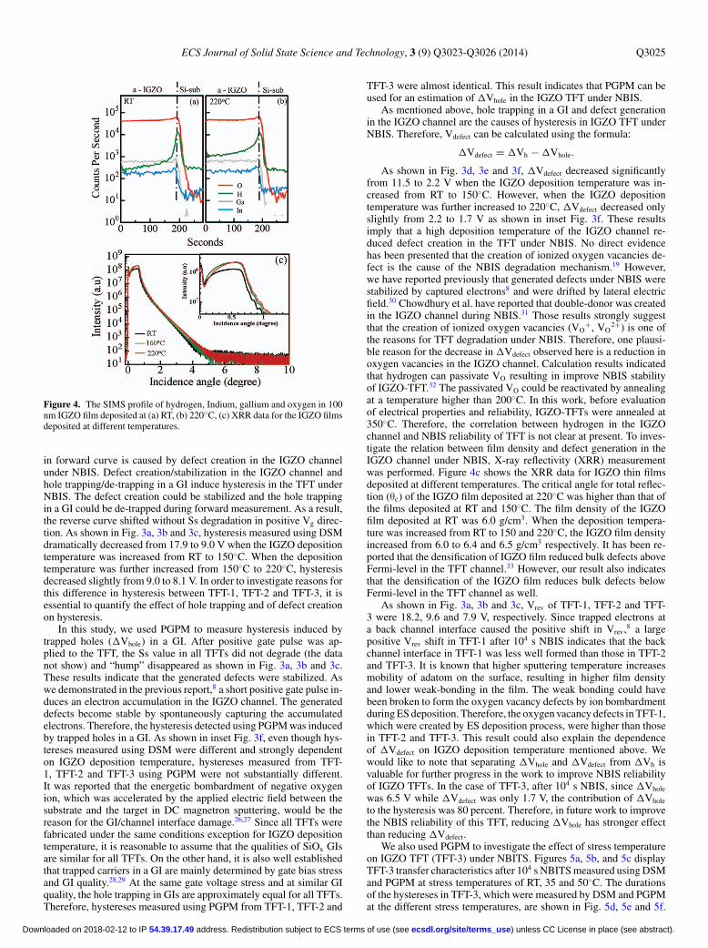
–7 × 10¹⁸ to –3 × 10¹⁹, resulting in the decrease in Vth mentionedabove. It is known that carrier mobility in an IGZO films increaseswith carrier concentration due to the potential barrier, which locatedin vicinity of conduction band edge, can be ovecome.1,20 However, ourresults show that the mobility decreases when carrier concentrationincreases. In order to investigate the reason, 100 nm IGZO film wasdeposited on high conductive Si substrate at RT and 220◦C. The com-position and hydrogen content in an IGZO film were evaluated usingthe secondary ion mass spectrometry (SIMS) measurement. Figure 4aand 4b show the composition distribution and hydrogen profile in anIGZO film deposited at RT and 220◦C respectively. Results of SIMSmeasurement show that In, Ga, O ion intensity in the channel didnot depend on the IGZO deposition temperature. However, hydrogenconcentration in the IGZO film deposited at 220◦C was higher thanthat in the films deposited at RT. The increasing hydrogen concentra-tion in the IGZO films with deposition temperature is consistent withthe deposition temperature dependence of the carrier concentration inIGZO and Vth mentioned above. The reason for the correlation be-tween carrier mobility and IGZO deposition temperature is not clearat present. However, It was reported that hydrogen plays not only asa shallow donor21 but also as a scattering center in the conductionpath.22,23 Therefore, the carrier scattering induced by hydrogen is onepossible reason for the decrease in carrier mobility mentioned above.The free hydrogen and hydrogen contained compounds in a sputteringchamber and in a sputtering target can play as the sources for hydrogenin IGZO film.24 It has been reported that the diffusion coefficient24
and solubility25 of hydrogen increase with temperature. As a result,the hydrogen contain in the IGZO film deposited at 220◦C was higherthan that deposited at RT.
The transfer characteristics measured using DSM and PGPM fromTFT-1, TFT-2 and TFT-3 after 104 s NBIS are shown in Fig. 3a, 3band 3c respectively. Figures 3d, 3e and 3f display the duration of Vh
measured from TFT-1, TFT-2 and TFT-3 using DSM and PGPM. Inforward curve measured by DSM, “hump” appeared, the reverse curveshifted positively, a hysteresis increased and on current decreased. Aswe reported in ref. 8, the electron trapping at back channel inter-face causes the positive shift in the reverse curve without mobilitydegradation. Therefore, on current degradation is due to positive shiftof Vth. Figure 3a, 3b, and 3c shows that on current degradation inTFT is proportional to positive shift in reverse curve. These resultsstrongly support our hypotheses that the electron trapping at a backchannel interface is a reason of a positive shift in reverse curve andof on current degradation. The ref. 8 also indicated that the “hump”
) unless CC License in place (see abstract). ecsdl.org/site/terms_use address. Redistribution subject to ECS terms of use (see 54.39.17.49Downloaded on 2018-02-12 to IP
ECS Journal of Solid State Science and Technology, 3 (9) Q3023-Q3026 (2014) Q3025
Figure 4. The SIMS profile of hydrogen, Indium, gallium and oxygen in 100nm IGZO film deposited at (a) RT, (b) 220◦C, (c) XRR data for the IGZO filmsdeposited at different temperatures.
in forward curve is caused by defect creation in the IGZO channelunder NBIS. Defect creation/stabilization in the IGZO channel andhole trapping/de-trapping in a GI induce hysteresis in the TFT underNBIS. The defect creation could be stabilized and the hole trappingin a GI could be de-trapped during forward measurement. As a result,the reverse curve shifted without Ss degradation in positive Vg direc-tion. As shown in Fig. 3a, 3b and 3c, hysteresis measured using DSMdramatically decreased from 17.9 to 9.0 V when the IGZO depositiontemperature was increased from RT to 150◦C. When the depositiontemperature was further increased from 150◦C to 220◦C, hysteresisdecreased slightly from 9.0 to 8.1 V. In order to investigate reasons forthis difference in hysteresis between TFT-1, TFT-2 and TFT-3, it isessential to quantify the effect of hole trapping and of defect creationon hysteresis.
In this study, we used PGPM to measure hysteresis induced bytrapped holes (�Vhole) in a GI. After positive gate pulse was ap-plied to the TFT, the Ss value in all TFTs did not degrade (the datanot show) and “hump” disappeared as shown in Fig. 3a, 3b and 3c.These results indicate that the generated defects were stabilized. Aswe demonstrated in the previous report,8 a short positive gate pulse in-duces an electron accumulation in the IGZO channel. The generateddefects become stable by spontaneously capturing the accumulatedelectrons. Therefore, the hysteresis detected using PGPM was inducedby trapped holes in a GI. As shown in inset Fig. 3f, even though hys-tereses measured using DSM were different and strongly dependenton IGZO deposition temperature, hystereses measured from TFT-1, TFT-2 and TFT-3 using PGPM were not substantially different.It was reported that the energetic bombardment of negative oxygenion, which was accelerated by the applied electric field between thesubstrate and the target in DC magnetron sputtering, would be thereason for the GI/channel interface damage.26,27 Since all TFTs werefabricated under the same conditions exception for IGZO depositiontemperature, it is reasonable to assume that the qualities of SiOx GIsare similar for all TFTs. On the other hand, it is also well establishedthat trapped carriers in a GI are mainly determined by gate bias stressand GI quality.28,29 At the same gate voltage stress and at similar GIquality, the hole trapping in GIs are approximately equal for all TFTs.Therefore, hystereses measured using PGPM from TFT-1, TFT-2 and
TFT-3 were almost identical. This result indicates that PGPM can beused for an estimation of �Vhole in the IGZO TFT under NBIS.
As mentioned above, hole trapping in a GI and defect generationin the IGZO channel are the causes of hysteresis in IGZO TFT underNBIS. Therefore, Vdefect can be calculated using the formula:
�Vdefect = �Vh − �Vhole.
As shown in Fig. 3d, 3e and 3f, �Vdefect decreased significantlyfrom 11.5 to 2.2 V when the IGZO deposition temperature was in-creased from RT to 150◦C. However, when the IGZO depositiontemperature was further increased to 220◦C, �Vdefect decreased onlyslightly from 2.2 to 1.7 V as shown in inset Fig. 3f. These resultsimply that a high deposition temperature of the IGZO channel re-duced defect creation in the TFT under NBIS. No direct evidencehas been presented that the creation of ionized oxygen vacancies de-fect is the cause of the NBIS degradation mechanism.19 However,we have reported previously that generated defects under NBIS werestabilized by captured electrons8 and were drifted by lateral electricfield.30 Chowdhury et al. have reported that double-donor was createdin the IGZO channel during NBIS.31 Those results strongly suggestthat the creation of ionized oxygen vacancies (VO
+, VO2+) is one of
the reasons for TFT degradation under NBIS. Therefore, one plausi-ble reason for the decrease in �Vdefect observed here is a reduction inoxygen vacancies in the IGZO channel. Calculation results indicatedthat hydrogen can passivate VO resulting in improve NBIS stabilityof IGZO-TFT.32 The passivated VO could be reactivated by annealingat a temperature higher than 200◦C. In this work, before evaluationof electrical properties and reliability, IGZO-TFTs were annealed at350◦C. Therefore, the correlation between hydrogen in the IGZOchannel and NBIS reliability of TFT is not clear at present. To inves-tigate the relation between film density and defect generation in theIGZO channel under NBIS, X-ray reflectivity (XRR) measurementwas performed. Figure 4c shows the XRR data for IGZO thin filmsdeposited at different temperatures. The critical angle for total reflec-tion (θc) of the IGZO film deposited at 220◦C was higher than that ofthe films deposited at RT and 150◦C. The film density of the IGZOfilm deposited at RT was 6.0 g/cm3. When the deposition tempera-ture was increased from RT to 150 and 220◦C, the IGZO film densityincreased from 6.0 to 6.4 and 6.5 g/cm3 respectively. It has been re-ported that the densification of IGZO film reduced bulk defects aboveFermi-level in the TFT channel.33 However, our result also indicatesthat the densification of the IGZO film reduces bulk defects belowFermi-level in the TFT channel as well.
As shown in Fig. 3a, 3b and 3c, Vrev of TFT-1, TFT-2 and TFT-3 were 18.2, 9.6 and 7.9 V, respectively. Since trapped electrons ata back channel interface caused the positive shift in Vrev,8 a largepositive Vrev shift in TFT-1 after 104 s NBIS indicates that the backchannel interface in TFT-1 was less well formed than those in TFT-2and TFT-3. It is known that higher sputtering temperature increasesmobility of adatom on the surface, resulting in higher film densityand lower weak-bonding in the film. The weak bonding could havebeen broken to form the oxygen vacancy defects by ion bombardmentduring ES deposition. Therefore, the oxygen vacancy defects in TFT-1,which were created by ES deposition process, were higher than thosein TFT-2 and TFT-3. This result could also explain the dependenceof �Vdefect on IGZO deposition temperature mentioned above. Wewould like to note that separating �Vhole and �Vdefect from �Vh isvaluable for further progress in the work to improve NBIS reliabilityof IGZO TFTs. In the case of TFT-3, after 104 s NBIS, since �Vhole
was 6.5 V while �Vdefect was only 1.7 V, the contribution of �Vhole
to the hysteresis was 80 percent. Therefore, in future work to improvethe NBIS reliability of this TFT, reducing �Vhole has stronger effectthan reducing �Vdefect.
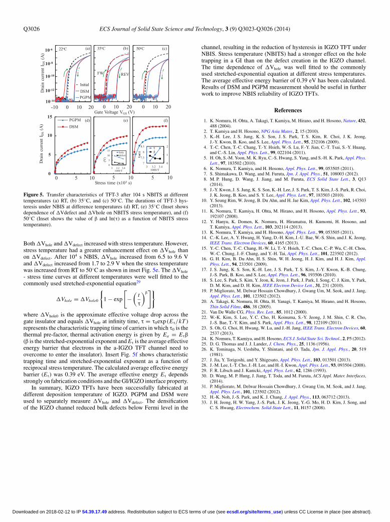
We also used PGPM to investigate the effect of stress temperatureon IGZO TFT (TFT-3) under NBITS. Figures 5a, 5b, and 5c displayTFT-3 transfer characteristics after 104 s NBITS measured using DSMand PGPM at stress temperatures of RT, 35 and 50◦C. The durationsof the hystereses in TFT-3, which were measured by DSM and PGPMat the different stress temperatures, are shown in Fig. 5d, 5e and 5f.
) unless CC License in place (see abstract). ecsdl.org/site/terms_use address. Redistribution subject to ECS terms of use (see 54.39.17.49Downloaded on 2018-02-12 to IP
Q3026 ECS Journal of Solid State Science and Technology, 3 (9) Q3023-Q3026 (2014)
RRT
RRT
22oC 35oC 50oC
10-14
10-12
10-10
10-8
10-6
Dra
in c
urre
nt I
DS
(A)
-10 0 10 20 0 10 20Gate Voltage VGS (V)
0 10 20
0
5
10
15
Dra
in c
urre
nt I
DS
(A)
0 5 10 5 10Stress time (x103 s)
5 10
(b)(a) (c)
(d) (e) (f)
0
1
2
7
7.5
8
8.5
3 3.2 3.41000/T
hole
b
τβ
Ln(
τ)
0
5
10
15
3 3.2 3.41000/T
holedefect
DSM
PGPM
EE-E-
DSM
PGPM
Initial
FW REV
Figure 5. Transfer characteristics of TFT-3 after 104 s NBITS at differenttemperatures (a) RT, (b) 35◦C, and (c) 50◦C. The durations of TFT-3 hys-teresis under NBIS at difference temperatures (d) RT, (e) 35◦C (Inset showsdependence of �Vdefect and �Vhole on NBITS stress temperature), and (f)50◦C (Inset shows the value of β and ln(τ) as a function of NBITS stresstemperature).
Both �Vhole and �Vdefect increased with stress temperature. However,stress temperature had a greater enhancement effect on �Vhole thanon �Vdefect. After 104 s NBIS, �Vhole increased from 6.5 to 9.6 Vand �Vdefect increased from 1.7 to 2.9 V when the stress temperaturewas increased from RT to 50◦C as shown in inset Fig. 5e. The �Vhole
- stress time curves at different temperatures were well fitted to thecommonly used stretched-exponential equation29
�Vhole = �Vhole0
{1 − exp
[−
(t
τ
)β]}
where �Vhole0 is the approximate effective voltage drop across thegate insulator and equals �Vhole at infinity time, τ = τ0exp (Eτ/kT )represents the characteristic trapping time of carriers in which τ0 is thethermal pre-factor, thermal activation energy is given by Ea = Eτβ(β is the stretched-exponential exponent and Eτ is the average effectiveenergy barrier that electrons in the a-IGZO TFT channel need toovercome to enter the insulator). Insert Fig. 5f shows characteristictrapping time and stretched-exponential exponent as a function ofreciprocal stress temperature. The calculated average effective energybarrier (Eτ) was 0.39 eV. The average effective energy Eτ dependsstrongly on fabrication conditions and the GI/IGZO interface property.
In summary, IGZO TFTs have been successfully fabricated atdifferent deposition temperature of IGZO. PGPM and DSM wereused to separately measure �Vhole and �Vdefect. The densificationof the IGZO channel reduced bulk defects below Fermi level in the
channel, resulting in the reduction of hysteresis in IGZO TFT underNBIS. Stress temperature (NBITS) had a stronger effect on the holetrapping in a GI than on the defect creation in the IGZO channel.The time dependence of �Vhole was well fitted to the commonlyused stretched-exponential equation at different stress temperatures.The average effective energy barrier of 0.39 eV has been calculated.Results of DSM and PGPM measurement should be useful in furtherwork to improve NBIS reliability of IGZO TFTs.
References
1. K. Nomura, H. Ohta, A. Takagi, T. Kamiya, M. Hirano, and H. Hosono, Nature, 432,488 (2004).
2. T. Kamiya and H. Hosono, NPG Asia Mater., 2, 15 (2010).3. K.-H. Lee, J. S. Jung, K. S. Son, J. S. Park, T. S. Kim, R. Choi, J. K. Jeong,
J.-Y. Kwon, B. Koo, and S. Lee, Appl. Phys. Lett., 95, 232106 (2009).4. T.-C. Chen, T.-C. Chang, T.-Y. Hsieh, W.-S. Lu, F.-Y. Jian, C.-T. Tsai, S.-Y. Huang,
and C.-S. Lin, Appl. Phys. Lett., 99, 022104 (2011).5. H. Oh, S.-M. Yoon, M. K. Ryu, C.-S. Hwang, S. Yang, and S.-H. K. Park, Appl. Phys.
Lett., 97, 183502 (2010).6. K. Nomura, T. Kamiya, and H. Hosono, Appl. Phys. Lett., 99, 053505 (2011).7. S. Shimakawa, D. Wang, and M. Furuta, Jpn. J. Appl. Phys., 51, 108003 (2012).8. M. P. Hung, D. Wang, J. Jiang, and M. Furuta, ECS Solid State Lett., 3, Q13
(2014).9. J.-Y. Kwon, J. S. Jung, K. S. Son, K.-H. Lee, J. S. Park, T. S. Kim, J.-S. Park, R. Choi,
J. K. Jeong, B. Koo, and S. Y. Lee, Appl. Phys. Lett., 97, 183503 (2010).10. Y. Seung Rim, W. Jeong, B. Du Ahn, and H. Jae Kim, Appl. Phys. Lett., 102, 143503
(2013).11. K. Nomura, T. Kamiya, H. Ohta, M. Hirano, and H. Hosono, Appl. Phys. Lett., 93,
192107 (2008).12. Y. Hanyu, K. Domen, K. Nomura, H. Hiramatsu, H. Kumomi, H. Hosono, and
T. Kamiya, Appl. Phys. Lett., 103, 202114 (2013).13. K. Nomura, T. Kamiya, and H. Hosono, Appl. Phys. Lett., 99, 053505 (2011).14. C.-K. Lee, A. Y. Hwang, H. Yang, D.-H. Kim, J.-U. Bae, W.-S. Shin, and J. K. Jeong,
IEEE Trans. Electron Devices, 60, 4165 (2013).15. Y.-C. Chen, T.-C. Chang, H.-W. Li, T.-Y. Hsieh, T.-C. Chen, C.-P. Wu, C.-H. Chou,
W.-C. Chung, J.-F. Chang, and Y.-H. Tai, Appl. Phys. Lett., 101, 223502 (2012).16. G. H. Kim, B. Du Ahn, H. S. Shin, W. H. Jeong, H. J. Kim, and H. J. Kim, Appl.
Phys. Lett., 94, 233501 (2009).17. J. S. Jung, K. S. Son, K.-H. Lee, J. S. Park, T. S. Kim, J.-Y. Kwon, K.-B. Chung,
J.-S. Park, B. Koo, and S. Lee, Appl. Phys. Lett., 96, 193506 (2010).18. S. Lee, S. Park, S. Kim, Y. Jeon, K. Jeon, J. Park, J. Park, I. Song, C. J. Kim, Y. Park,
D. M. Kim, and D. H. Kim, IEEE Electron Device Lett., 31, 231 (2010).19. P. Migliorato, M. Delwar Hossain Chowdhury, J. Gwang Um, M. Seok, and J. Jang,
Appl. Phys. Lett., 101, 123502 (2012).20. A. Takagi, K. Nomura, H. Ohta, H. Yanagi, T. Kamiya, M. Hirano, and H. Hosono,
Thin Solid Films, 486, 38 (2005).21. Van De Walle CG, Phys. Rev. Lett., 85, 1012 (2000).22. W.-K. Kim, S. Lee, Y. C. Cho, H. Koinuma, S.-Y. Jeong, J. M. Shin, C. R. Cho,
J.-S. Bae, T.-Y. Kim, and S. Park, Appl. Phys. Lett., 98, 122109 (2011).23. S. Oh, G. Choi, H. Hwang, W. Lu, and J.-H. Jang, IEEE Trans. Electron Devices, 60,
2537 (2013).24. K. Nomura, T. Kamiya, and H. Hosono, ECS J. Solid State Sci. Technol., 2, P5 (2012).25. D. G. Thomas and J. J. Lander, J. Chem. Phys., 25, 1136 (1956).26. K. Tominaga, N. Ueshiba, Y. Shintani, and O. Tada, Jpn. J. Appl. Phys., 20, 519
(1981).27. J. Jia, Y. Torigoshi, and Y. Shigesato, Appl. Phys. Lett., 103, 013501 (2013).28. J.-M. Lee, I.-T. Cho, J.-H. Lee, and H.-I. Kwon, Appl. Phys. Lett., 93, 093504 (2008).29. F. R. Libsch and J. Kanicki, Appl. Phys. Lett., 62, 1286 (1993).30. D. Wang, M. P. Hung, J. Jiang, T. Toda, and M. Furuta, ACS Appl. Mater. Interfaces,
(2014).31. P. Migliorato, M. Delwar Hossain Chowdhury, J. Gwang Um, M. Seok, and J. Jang,
Appl. Phys. Lett., 101, 123502 (2012).32. H.-K. Noh, J.-S. Park, and K. J. Chang, J. Appl. Phys., 113, 063712 (2013).33. J. H. Jeong, H. W. Yang, J.-S. Park, J. K. Jeong, Y.-G. Mo, H. D. Kim, J. Song, and
C. S. Hwang, Electrochem. Solid-State Lett., 11, H157 (2008).
) unless CC License in place (see abstract). ecsdl.org/site/terms_use address. Redistribution subject to ECS terms of use (see 54.39.17.49Downloaded on 2018-02-12 to IP