qualitative discussion of mos transistors. big picture es220 (electric circuits) – r, l, c,...
TRANSCRIPT

Qualitative Discussion of MOS Transistors

Big Picture
• ES220 (Electric Circuits)– R, L, C, transformer, op-amp
• ES230 (Electronics I)– Diodes– BJT– Complementary Metal Oxide Semiconductor
(CMOS) Field Effect Transistor (FET)• Applications in Digital Integrated Circuits
• ES330 (Electronics II)– Explore Applications of CMOS in Analog Integrated
Circuits

Topics Covered in ES330
• Small Signal Model• Body Effect

A Crude Metal Oxide Semiconductor (MOS) Device
P-Type Silicon is slightly conductive.
Positive charge attractnegative chargesto interface between insulator and silicon.
A conductive path is createdIf the density of electrons is sufficiently high.Q=CV.
V2 causes movement of negative charges,thus current.
V1 can control the resistivity of the channel.The gate
draws no current!

An Improved MOS Transistor
n+ diffusion allowselectrons movethrough silicon.
(provide electrons) (drain electrons)
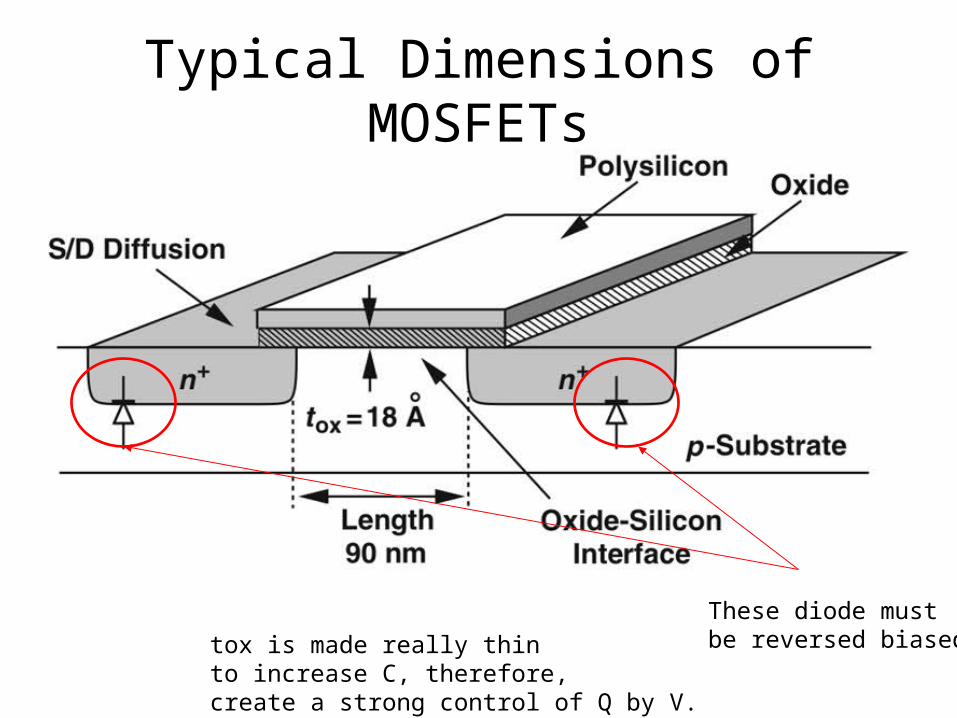
Typical Dimensions of MOSFETs
These diode mustbe reversed biased.tox is made really thin
to increase C, therefore, create a strong control of Q by V.
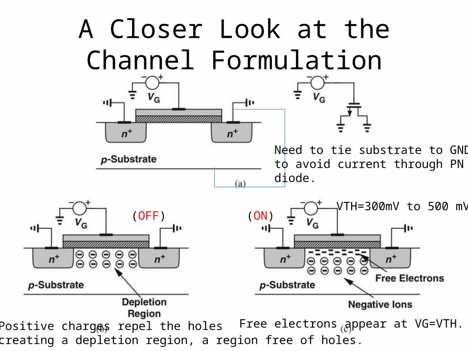
A Closer Look at the Channel Formulation
Need to tie substrate to GNDto avoid current through PN diode.
Positive charges repel the holescreating a depletion region, a region free of holes.
Free electrons appear at VG=VTH.
VTH=300mV to 500 mV(OFF) (ON)

MOSFET as a Variable Resistor
As VG increases, the density of electrons increases, the value ofchannel resistance changes with gate voltage.
You can build anattenuator circuit. (i.e. a voltage divider)

Change Drain Voltage
Resistance determined by VG.
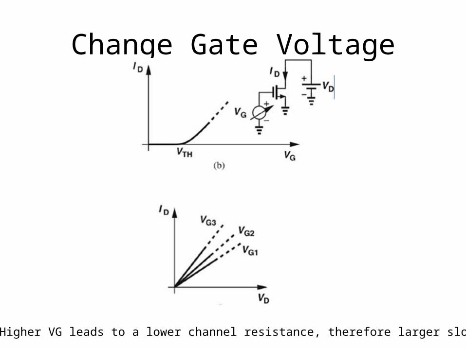
Change Gate Voltage
Higher VG leads to a lower channel resistance, therefore larger slope.

Length Dependence
The resistance of a conductor is proportional to the length.
fixed VD
fixed VG

Dependence on Oxide Thickness
Q=CVC is inversely proportional to 1/tox.
Lower Q implies higher channel resitsance.
fixed VD fixed VG

Width Dependence
The resistance of a conductor is inversely proportional to the crosssection area.
A larger device also has a larger capacitance!

Channel Pinch Off• Q=CV– V=VG-VOXIDE-Silicon
• VOXIDE-Silicon can change along the channel! Low VOXIDE-Silicon implies less Q.

VG-VD is sufficiently largeto produce a channel
VG-VD is NOT sufficiently largeto produce a channel
No channel
Electronsare sweptby E to drain.
Drain can no longer affect the drain current!

Regions
No channel
(No Dependence on VDS)

Determination of Region
• How do you know whether a transistor is in the linear region or saturation region?– If VDS>(VGS-VTH) and VGS>VTH, then
the device is in the saturation region.– If VDS<(VGS-VTH) and VGS>VTH, then
the device is in the linear region.

Graphical Illustration

Limited VDS Dependence During Saturation
As VDS increase, effective L decreases, therefore, ID increases.

Pronounced Channel Length Modulation in small L
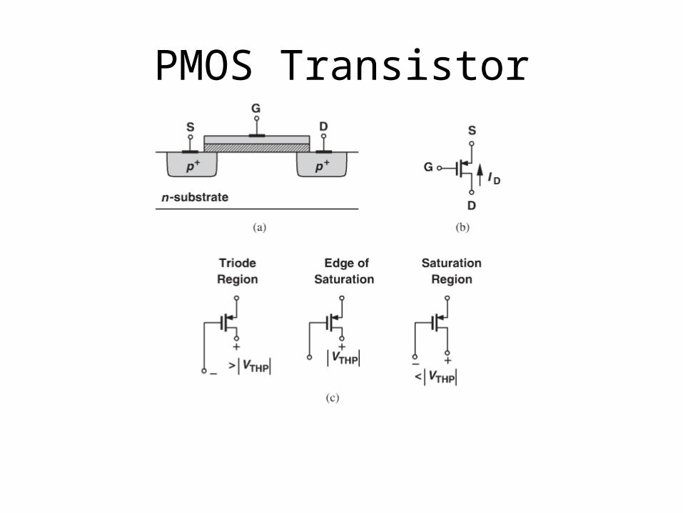
PMOS Transistor

IV Characteristics of a PMOS