pure.tue.nl · de promotiecommissie bestaat uit: prof.dr. b. koopmans 1e promotor, techn....
TRANSCRIPT

Key concepts in spin tunneling : amorphous ferromagnets forspintronicsCitation for published version (APA):Paluskar, P. V. (2008). Key concepts in spin tunneling : amorphous ferromagnets for spintronics. TechnischeUniversiteit Eindhoven. https://doi.org/10.6100/IR635545
DOI:10.6100/IR635545
Document status and date:Published: 01/01/2008
Document Version:Publisher’s PDF, also known as Version of Record (includes final page, issue and volume numbers)
Please check the document version of this publication:
• A submitted manuscript is the version of the article upon submission and before peer-review. There can beimportant differences between the submitted version and the official published version of record. Peopleinterested in the research are advised to contact the author for the final version of the publication, or visit theDOI to the publisher's website.• The final author version and the galley proof are versions of the publication after peer review.• The final published version features the final layout of the paper including the volume, issue and pagenumbers.Link to publication
General rightsCopyright and moral rights for the publications made accessible in the public portal are retained by the authors and/or other copyright ownersand it is a condition of accessing publications that users recognise and abide by the legal requirements associated with these rights.
• Users may download and print one copy of any publication from the public portal for the purpose of private study or research. • You may not further distribute the material or use it for any profit-making activity or commercial gain • You may freely distribute the URL identifying the publication in the public portal.
If the publication is distributed under the terms of Article 25fa of the Dutch Copyright Act, indicated by the “Taverne” license above, pleasefollow below link for the End User Agreement:www.tue.nl/taverne
Take down policyIf you believe that this document breaches copyright please contact us at:[email protected] details and we will investigate your claim.
Download date: 25. Jul. 2020


Key Concepts in Spin Tunneling
Amorphous Ferromagnets for Spintronics
Paresh Vijay Paluskar

De promotiecommissie bestaat uit:prof.dr. B. Koopmans 1e promotor, Techn. Universiteit Eindhovenprof.dr.ir. H.J.M. Swagten 2e promotor, Techn. Universiteit EindhovenDr.rer.nat. J.T. Kohlhepp copromotor, Techn. Universiteit Eindhoven
prof.dr. R. Coehoorn lid kerncommissie, Techn. Universiteit Eindhovenen Philips Research Laboratories
dr. C.F.J. Flipse lid kerncommissie, Techn. Universiteit Eindhovenprof.dr. R.A. de Groot lid kerncommissie, Radboud Universiteit NijmegenDr. J.S. Moodera lid kerncommissie, Massachusetts Inst. of Tech.
The work described in this thesis has been carried out in the group Physics of Nanos-tructures, at the Department of Applied Physics, Eindhoven University of Technol-ogy, the Netherlands.
This research was supported by NanoNed, a national nanotechnology program co-ordinated by the Dutch Ministry of Economic Affairs. Flagship NanoSpintronics.Project number 6474/7152 - 1B1.
The cover shows the k-resolved density of states of fcc Co at the Fermi level. Artistsimpression by P.V. Paluskar and data from G.A. de Wijs, J.J. Attema and R.A. de Groot(Radboud Universiteit Nijmegen).

Key Concepts in Spin Tunneling
Amorphous Ferromagnets for Spintronics
Proefschrift
ter verkrijging van de graad van doctoraan de Technische Universiteit Eindhoven
op gezag van de Rector Magnificus, prof.dr.ir. C.J. van Duijn,voor een commissie aangewezen door het Collegevoor Promoties in het openbaar te verdedigen op
dinsdag 1 juli 2008 om 16.00 uur
door
Paresh Vijay Paluskar
geboren te Pandharpur, India
Dit proefschrift is goedgekeurd door de promotoren:
prof.dr. B. Koopmansenprof.dr.ir. H.J.M. Swagten
Copromotor:Dr.rer.nat. J.T. Kohlhepp
CIP- DATA LIBRARY TECHNISCHE UNIVERSITEIT EINDHOVEN
Paluskar, Paresh Vijay
Key Concepts in Spin Tunneling : Amorphous Ferromagnets for Spintronics by /Paresh Vijay Paluskar. - Eindhoven : Technische Universiteit Eindhoven, 2008. -Proefschrift.ISBN: 978-90-386-1296-6NUR 926Trefwoorden: spinpolarisatie/supergeleiding/tunneljuncties/amorfe ferromagnetenSubject Headings: spin polarization/superconductivity/tunnel junctions/amorphousferromagnets
Printed By: Universiteitsdrukkerij Technische Universiteit Eindhoven.

Dedicated to my family,
my parents Prabha and Vijay,my wife Sonu,
and my brother Parag

vi

Contents
1 Introduction to spin tunneling 1
1.1 Spintronics in daily life . . . . . . . . . . . . . . . . . . . . . . . . . . 2
1.2 Basic aspects . . . . . . . . . . . . . . . . . . . . . . . . . . . . . . . 3
1.2.1 Electronic structure of 3d TM FMs . . . . . . . . . . . . . . . 3
1.2.2 Electron and spin tunneling . . . . . . . . . . . . . . . . . . . 5
1.3 Contemporary notions on spin tunneling . . . . . . . . . . . . . . . . 9
1.3.1 AlOx: Relevant experiments . . . . . . . . . . . . . . . . . . . 10
1.3.2 MgO: Relevant experiments . . . . . . . . . . . . . . . . . . . 13
1.4 Relevance of amorphous ferromagnets . . . . . . . . . . . . . . . . . . 15
1.5 This thesis . . . . . . . . . . . . . . . . . . . . . . . . . . . . . . . . . 16
Bibliography . . . . . . . . . . . . . . . . . . . . . . . . . . . . . . . . . . 18
2 Probing electronic, magnetic and structural properties 23
2.1 Sample fabrication . . . . . . . . . . . . . . . . . . . . . . . . . . . . 24
2.1.1 Substrate and substrate cleaning considerations . . . . . . . . 24
2.1.2 Deposition: Sputtering . . . . . . . . . . . . . . . . . . . . . . 24
2.1.3 Plasma oxidation . . . . . . . . . . . . . . . . . . . . . . . . . 28
2.2 Structural characterization . . . . . . . . . . . . . . . . . . . . . . . . 28
2.2.1 X-ray diffraction (XRD) . . . . . . . . . . . . . . . . . . . . . 29
2.2.2 X-ray absorption fine structure (XAFS) . . . . . . . . . . . . . 31
2.2.3 High-resolution transmission electron microscopy (HRTEM) . 35
2.3 In-situ analysis of chemical and electronic properties . . . . . . . . . . 35
2.3.1 X-ray photoelectron spectroscopy (XPS) . . . . . . . . . . . . 35
2.3.2 Ultraviolet photoelectron spectroscopy (UPS) . . . . . . . . . 39
2.4 Magnetic characterization . . . . . . . . . . . . . . . . . . . . . . . . 39
2.4.1 Superconducting quantum interference device (SQUID) . . . . 40
2.4.2 Magneto-optical Kerr effect (MOKE) . . . . . . . . . . . . . . 40
2.4.3 Magnetic circular dichroism (XMCD) in x-ray absorption (XAS) 43
2.5 Measuring electronic transport . . . . . . . . . . . . . . . . . . . . . . 49
2.5.1 Superconduction tunneling spectroscopy (STS) . . . . . . . . . 49
vii

viii CONTENTS
2.5.2 Inelastic electron tunneling spectroscopy (IETS) . . . . . . . . 55
2.5.3 Magnetoresistance (MR) . . . . . . . . . . . . . . . . . . . . . 57
2.5.4 Current in-plane tunneling (CIPT) . . . . . . . . . . . . . . . 57
Bibliography . . . . . . . . . . . . . . . . . . . . . . . . . . . . . . . . . . 65
3 Magnetic properties of CoFeB 71
3.1 Background . . . . . . . . . . . . . . . . . . . . . . . . . . . . . . . . 72
3.2 Sample preparation . . . . . . . . . . . . . . . . . . . . . . . . . . . . 72
3.3 Properties of Co72Fe20B8 . . . . . . . . . . . . . . . . . . . . . . . . . 74
3.3.1 Crystallization of Co72Fe20B8 . . . . . . . . . . . . . . . . . . 74
3.3.2 Effect of Co72Fe20B8 crystallization on film resistance . . . . . 75
3.3.3 Effect of Co72Fe20B8 crystallization on magnetic properties . . 76
3.4 Properties of Co80-xFexB20 . . . . . . . . . . . . . . . . . . . . . . . . 78
3.4.1 Crystallization of Co80-xFexB20 from XRD . . . . . . . . . . . 78
3.4.2 Effect of Co60Fe20B20 crystallization on magnetic properties . . 78
3.5 Summary . . . . . . . . . . . . . . . . . . . . . . . . . . . . . . . . . 81
Bibliography . . . . . . . . . . . . . . . . . . . . . . . . . . . . . . . . . . 82
4 Key concepts in spin tunneling 85
4.1 Introduction . . . . . . . . . . . . . . . . . . . . . . . . . . . . . . . . 86
4.1.1 Background . . . . . . . . . . . . . . . . . . . . . . . . . . . . 86
4.1.2 Objectives of this work . . . . . . . . . . . . . . . . . . . . . . 87
4.2 Experimental Results . . . . . . . . . . . . . . . . . . . . . . . . . . . 88
4.2.1 Sample preparation and measurement . . . . . . . . . . . . . . 88
4.2.2 Impact of CoFeB crystallization of its TSP . . . . . . . . . . . 90
4.2.3 Verification of crystallization at interface . . . . . . . . . . . . 90
4.3 Comparison of calculated and measured a-CoFeB . . . . . . . . . . . 93
4.3.1 Calculation: Molecular dynamics . . . . . . . . . . . . . . . . 93
4.3.2 Measurements: molecular dynamics vs. EXAFS . . . . . . . . 93
4.4 Electronic structure and TSP . . . . . . . . . . . . . . . . . . . . . . 94
4.4.1 Fe in strongly ferromagnetic state . . . . . . . . . . . . . . . . 94
4.4.2 Comparison with measured TSP . . . . . . . . . . . . . . . . . 94
4.4.3 Interface bonding effects . . . . . . . . . . . . . . . . . . . . . 96
4.4.4 Changes in electronic structure on crystallization . . . . . . . 97
4.4.5 Highly spin-polarized boron sp states . . . . . . . . . . . . . . 97
4.5 Conclusions . . . . . . . . . . . . . . . . . . . . . . . . . . . . . . . . 98
Bibliography . . . . . . . . . . . . . . . . . . . . . . . . . . . . . . . . . . 99
5 Impact of interface crystallization on inelastic tunneling 103
5.1 Introduction . . . . . . . . . . . . . . . . . . . . . . . . . . . . . . . . 104

CONTENTS ix
5.1.1 Background: Interface scattering . . . . . . . . . . . . . . . . 104
5.1.2 Background: Inelastic electron tunneling spectroscopy (IETS) 104
5.2 This work . . . . . . . . . . . . . . . . . . . . . . . . . . . . . . . . . 104
5.3 Experimental Methods . . . . . . . . . . . . . . . . . . . . . . . . . . 105
5.3.1 Sample preparation and measurement . . . . . . . . . . . . . . 105
5.3.2 Verification of crystallization at interface . . . . . . . . . . . . 105
5.4 Experimental Results . . . . . . . . . . . . . . . . . . . . . . . . . . . 105
5.4.1 IETS spectra: Phonon modes . . . . . . . . . . . . . . . . . . 105
5.4.2 IETS spectra: Magnon modes . . . . . . . . . . . . . . . . . . 107
5.4.3 Size quantization of magnon modes . . . . . . . . . . . . . . . 108
5.4.4 Zero bias anomaly . . . . . . . . . . . . . . . . . . . . . . . . 110
5.5 Summary . . . . . . . . . . . . . . . . . . . . . . . . . . . . . . . . . 110
Bibliography . . . . . . . . . . . . . . . . . . . . . . . . . . . . . . . . . . 111
6 Correlation between magnetism and TSP 115
6.1 Background . . . . . . . . . . . . . . . . . . . . . . . . . . . . . . . . 116
6.2 This work and the relevance to understanding CoFeB . . . . . . . . . 116
6.3 Sample preparation and measurement . . . . . . . . . . . . . . . . . . 117
6.4 Introduction to the S−P behavior . . . . . . . . . . . . . . . . . . . . 118
6.4.1 Basic aspects from computational magnetism . . . . . . . . . 118
6.4.2 S−P behavior of CoFeB . . . . . . . . . . . . . . . . . . . . . 120
6.5 TSP of CoFeB shows the S−P behavior . . . . . . . . . . . . . . . . . 120
6.6 Changes in valance band structure - UPS data . . . . . . . . . . . . . 122
6.7 XAS and XMCD . . . . . . . . . . . . . . . . . . . . . . . . . . . . . 123
6.7.1 Orbital moment (mo) . . . . . . . . . . . . . . . . . . . . . . . 123
6.7.2 Spin moment (ms) and exchange splitting (∆ex) . . . . . . . . 125
6.8 Correlation between the s and the d -bands . . . . . . . . . . . . . . . 125
6.9 Discussion on CoFe . . . . . . . . . . . . . . . . . . . . . . . . . . . . 126
6.10 Conclusions . . . . . . . . . . . . . . . . . . . . . . . . . . . . . . . . 126
A Appendix . . . . . . . . . . . . . . . . . . . . . . . . . . . . . . . . . 127
A.1 Difference between Fe and Fe80B20 - XAS . . . . . . . . . . . . 127
A.2 Band-Filling and orbital moment . . . . . . . . . . . . . . . . 128
A.3 Orbital moment . . . . . . . . . . . . . . . . . . . . . . . . . . 129
A.4 Ratio of Orbital to Spin Moment . . . . . . . . . . . . . . . . 129
A.5 Co edge XAS and XMCD . . . . . . . . . . . . . . . . . . . . 130
Bibliography . . . . . . . . . . . . . . . . . . . . . . . . . . . . . . . . . . 131
7 Thermal stability of MTJs 135
7.1 Introduction . . . . . . . . . . . . . . . . . . . . . . . . . . . . . . . . 136

x CONTENTS
7.1.1 Background . . . . . . . . . . . . . . . . . . . . . . . . . . . . 136
7.1.2 This work . . . . . . . . . . . . . . . . . . . . . . . . . . . . . 136
7.2 Experimental Results . . . . . . . . . . . . . . . . . . . . . . . . . . . 137
7.2.1 Confirmation of Mn diffusion in a MTJ . . . . . . . . . . . . . 137
7.2.2 Does Mn diffuse? . . . . . . . . . . . . . . . . . . . . . . . . . 138
7.2.3 Influence of Mn diffusion on the TSP . . . . . . . . . . . . . . 140
7.2.4 Impact of annealing on TSP . . . . . . . . . . . . . . . . . . . 141
7.3 Summary . . . . . . . . . . . . . . . . . . . . . . . . . . . . . . . . . 142
Bibliography . . . . . . . . . . . . . . . . . . . . . . . . . . . . . . . . . . 143
Summary 145
List of publications 148
About the author 150
Acknowledgements 151

Chapter 1
Introduction to spin tunneling
Ferromagnets and magnetic tunnel junctions in spintronics
Abstract: In this chapter1 we will introduce some relevant aspects of the elec-tronic structure of ferromagnets, and how spintronic devices like MTJs employ thiselectronic structure for device operation. Then we will introduce a few experimentsfrom which we derive our existing notions about the physics of spin tunneling. Noattempt will be made to be complete or exhaustive in this section. Instead, thereader is referred to suitable reviews which embark on such an exhaustive overview.Subsequently, we will talk about a novel ferromagnetic material − CoFeB − whichhas the potential for advancing the application of spintronic devices. In the lastpart of the chapter, we will outline this thesis.
1A large part of this chapter will appear as a review in the Encyclopedia of Materials Scienceand Technology authored by H.J.M. Swagten and P.V.Paluskar [62].
1

2 Chapter 1 Introduction to spin tunneling
1.1 Spintronics in daily life
The fact that electrons have a spins, i.e., an intrinsic magnetic moment, plays animportant role in our everyday life. Technologies that use these electron-spins are notcompletely unknown in the daily life of a common man. One example is the magneticstrip on credit cards, another is a magnetic compass which navigates automobiles.A recent discovery which uses these electron-spins in electronic devices has spurredanother wave of technology in the realm of data storage and sensing. It has, inessence, revolutionized the way we carry personal digital information, and therefore,not surprisingly, has been awarded the Nobel prize for Physics in 2007. Indeed, hereone refers to the giant magnetoresistance effect (GMR) and the field of research thatengenders from it - spintronics / magnetoelectronics. The most popular product thatuses this technology is a computer hard-disk where information is read using a GMRsensor. Due to the use of these sensors, the density of information that can be storedon a hard-disk has increased substantially, allowing the emergence of products likethe i-POD. This thesis is placed in this field, where the physical effects and devicesbased on electron-spins are explored.
Let us have a look at the essentials of spin-transport in such devices. A sketch ofGMR device is shown in Figure 1.1(a). Here, two ferromagnetic layers (for example,Co or Fe) are separated by a non-magnetic layer (for example, Cu or Cr). Assumethat, using an external magnetic field, the magnetization of these two layers can bealigned parallel to each other [see Figure 1.1(a)] or antiparallel to each other [seeFigure 1.1(b)]. When a current flows through this trilayer, the electrons which havetheir spins aligned with the magnetization of the layer experience less scatteringevents. On the other hand, the electrons with spins pointing opposite to the layermagnetization experience more scattering events. Therefore, in a parallel configura-tion, there are always electrons of one spin type that can easily travel through thetrilayer. In Figure 1.1(a), this would be the case with the spin pointing right, whichwe call a spin-up or majority electron. We call the other electron, with spin pointingleft, the spin-down or minority electron. Coming to the antiparallel configurationshown in Figure 1.1(b), one notices that although the spin-up electron manages toreach the top layer, its magnetization is aligned opposite to the local magnetiza-tion. Therefore, this electron too experiences more scattering events. Now, morescattering events implies that the electrons ‘feel’ a higher resistance while travers-ing the trilayer. Since in the antiparallel configuration, both spin-up and spin-downelectrons experience more scattering events, the resistance of the trilayer in this con-figuration is high. On the contrary, the parallel configuration allows easy transportof spin-up electrons, and the device resistance is comparatively low. This change inresistance which depends on the relative alignment of the magnetization of the twoferromagnetic layers is called magnetoresistance, and is defined as

1.2 Basic aspects 3
MR =RAP −RP
RP
× 100% (1.1)
where P and AP denote parallel and antiparallel configuration. The resistance ofsuch a device is shown in Figure 1.1(c) where MR is plotted as a function of the ap-plied external field. At very high positive or negative fields (in this case, ±30 kA/m),the layers are aligned parallel, the resistance is low and the MR is zero. However,these layers are so engineered that in external fields of 7−10 kA/m, the antiparallelconfiguration is achieved, and the observed resistance and MR is high.
In 1988−89, two groups (that of Albert Fert and Peter Grunberg) reported theobservation of a such a magnetoresistance effect [1, 2]. The change in resistanceobserved in [Fe/Cr]n multilayers was almost 50%, which led to the name giant mag-netoresistance effect. Since then, significant progress has been made in enhancingthe observed effect, as well as in understanding the origin of the effect. The readermay refer to extended reviews on this topic [3, 4].
Such spin-dependent electronic transport was subsequently observed in anothertype of device called a magnetic tunnel junction (MTJ). In this case, the non-magnetic spacer layer of Figure 1.1(a-b) is replaced by a thin insulator (∼25 A thick).Given the fact that quantum mechanics allows electrons to tunnel through such athin insulator, one may imagine that electronic transport from one ferromagneticlayer to the other across such a tunnel barrier would also lead to a magnetoresis-tance effect. In 1995, Moodera et al. [5] and Miyazaki et al. [6] reported such amagnetoresistance effect which is appropriately called tunneling magnetoresistance(TMR). Considering that a decade later TMR effects above 200% have been re-ported, the application potential of such devices has not gone unrecognized. In fact,many technological devices which envision the use of this effect have been proposed,and some are already commercially available.
This thesis investigates the properties and fundamental aspects of electron, andconsequently, spin tunneling in such tunnel junctions. In the rest of this chapter, wewill briefly review some basic ideas in this field and introduce some existing notionswhich constitute the basis of our understanding of this effect.
1.2 Basic aspects
1.2.1 Electronic structure of 3d TM FMs
Elemental 3d transition metal (TM) ferromagnets (FM) like Fe, Co, and Ni andalloys derived from them have intrigued humans from time immemorial. Fromprimeval amazement regarding the magnetic compass and its implication that theearth itself was a giant magnet, and the apparent magical power of magnets in at-tracting and sticking to metals like iron, to existing controversies on magnetorecep-tion in animals and birds, and the intriguing field of planetary magnetism, humans

4 Chapter 1 Introduction to spin tunneling
Figure 1.1: Origin of spin dependent transport. Schematic representation ofspin dependent transport and the origin of the GMR effect in magnetic multilayers.(a) parallel configuration: majority electrons (spins aligned with local magnetiza-tion) traverse layers with lower scattering events as compared to minority electrons(spins aligned against local magnetization) (b) antiparallel configuration: each spinspecies scatters in one of the two ferromagnetic layers. Therefore, the comparativeresistance in this antiparallel configuration is higher than the parallel configuration.(c) Example MR curve where the resistance is plotted as a function of the appliedfield. At large fields, positive or negative, the resistance is low due to the parallelconfiguration. Closer to zero, the trilayer is engineered to achieve antiparallel con-figuration in one field direction (negative field in this case). In Figure (c), note thatalthough the MR curve is not measured on a GMR stack but a TMR stack, theprimary difference is only in the magnitude of the MR effect.
are yet to conquer the mysteries cast by magnetism. However, all throughout, oursearch for answers has been fervent, to say the least. In this section, we will try tobriefly sketch the basic concepts on the question “why metals like Fe, Co and Ni areferromagnetic?”

1.2 Basic aspects 5
The essential aspects are that electrons have intrinsic spins, and their wave func-tions have different spatial symmetries. These wave functions are allowed to ac-commodate only a certain number of electrons. When placed in a solid, the wavefunctions form bands which electrons occupy in k -space. In 3d TMs, the d -bands lieclose to the Fermi level and may accommodate 10 electrons. Their band widths arein the order of 5 eV; much smaller than the band widths of spherically symmetric de-localized s-bands. Because of this narrow band width which needs to accommodate10 electrons, the electronic density is high, and the Fermi surface is dominated bycontributions from the d -bands. Naturally, this high density of states of 3d -electronsat the Fermi level also greatly influences the electronic and magnetic properties ofthe solid.
The magnetic properties of 3d TMs are a consequence of the fact that the elec-tronic wave function is required to be antisymmetric, either in its spin or spatialpart. This, together with the narrow band width of 3d TMs which allows greaterelectron density, is the cause of a collective magnetic moment in 3d TM FMs. Inorder to minimize coulomb repulsion, the electrons tend to couple with their spinsparallel, which forces antisymmetric spatial wave functions. This is, in essence,Hund’s first rule for free atoms which renders almost 80% of the periodic table ina high spin-state. In a solid however, electrons become delocalized and the gain inexchange energy which aligns spins parallel must overcome the additional kineticenergy to put the spins in the same spin-band. Therefore, the more the electronicsystem becomes delocalized, the smaller the chance to display ferromagnetism. For,Fe, Co and Ni, the narrow d -band comes to rescue where the large density of states(DOS) at the EF satisfies the Stoner criterion for ferromagnetism N(EF ) · I > 1,where I is the Stoner parameter and represents intra-atomic exchange and correla-tion effects. In other words, for these elements, the DOS [N(EF )] is large enoughfor parallel (ferromagnetic) coupling of spins without increasing the kinetic energyof the d -bands considerably. This energy is called the exchange splitting and istypically ∼1 eV. As an example the DOS of Co in a ternary alloy of CoFeB is shownin Figure 1.2 [7]. The resulting spin magnetic moment is given by
ms = (N↑ −N↓) µB (1.2)
that is, the difference between the occupation of the spin-up and spin-down bands.Analyzing the contribution of the various types of electrons in 3d TM FMs (differentspatial symmetries of the wave function), one finds that the spin moments of the d -electrons contribute ∼90% to the total moment, while their orbital moment is almostcompletely quenched in a solid. The 4sp electrons carry no orbital moment [8, 9],and their spin moments contribute ∼5% to the total moment.
1.2.2 Electron and spin tunneling
It is well-known that when an insulator is made very thin, of the order of a fewnanometer, electrons can tunnel through this thin insulator according to laws of

6 Chapter 1 Introduction to spin tunneling
-10 -8 -6 -4 -2 0 2 4-2
-1
0
1
2
-0.10
-0.05
0.00
0.05
0.10 d d
d-D
OS
(sta
tes/
eV/a
tom
)
Energy (eV)
s s
s-D
OS
(sta
tes/
eV/a
tom
)
Figure 1.2: Density of states of a ferromagnet. Representative DOS of Coin CoFeB which shows s-DOS and d -DOS. Here the states/eV/atom are plottedas a function of energy and EF is set to zero. The s-DOS is magnified ∼20 timesfor comparison with the d -DOS. Please refer to Paluskar et al. [7] or Chapter 4 fordetails.
quantum mechanics. Regarding the spin of these tunneling electrons, it is assumedto conserve if the electron tunnels elastically. Spin tunneling becomes relevant in thecase of magnetic tunnel junctions (MTJs), where the insulator is sandwiched betweentwo ferromagnets, as shown in Figure 1.3. In such a device, the magnitude of thetunneling current depends on the relative orientation of the magnetization of bothelectrodes. When the magnetization of the two electrodes is aligned parallel, a largecurrent flows, while an antiparallel alignment of the two electrodes results in a smallcurrent. This can be understood from a few elementary arguments. (i) The tunnelingcurrent is in first order proportional to the product of the electrode’s density of statesat the Fermi level [N(EF )]. (ii) As we noted in the previous section, in a ferromagnet,the ground-state energy bands in the vicinity of the Fermi level are shifted in energydue to exchange splitting, yielding unequal majority and minority bands for electronswith opposite spins. (iii) Assuming spin conservation for the tunneling electrons,there are two separate currents of spin up and spin down character. As a resultof these ingredients, the current between electrodes with the same magnetizationdirection should be higher than for oppositely magnetized electrodes. This is furtherillustrated in the right panel of Figure 1.3. Within this simple so-called Jullieremodel, the resistance change is called tunneling magnetoresistance (normalized tothe lowest resistance) is given by:
TMR =2P1P2
1− P1P2
(1.3)

1.2 Basic aspects 7
EF
EF
N1
majN
2
majN
1
minN
2
min
ba
rrie
rb
arr
ier
large current
small current
Figure 1.3: Spin-polarized tunneling in MTJs. Schematic illustration ofthe physics behind tunnel magnetoresistance. Top: for parallel aligned magneti-zation as sketched in the left, electrons around the Fermi level with spin-up (↑)and spin-down (↓) are allowed to tunnel from majority→majority bands, andfrom minority⇒minority bands. Bottom: when the magnetization of the twoferromagnets is anti-parallel, tunneling takes place for majority→minority andminority→majority bands, leading to a reduction of total tunneling current. Interms of electrical resistance, this corresponds to a higher resistance when the mag-netization of the two layers are oppositely aligned.
with
P1,2 =Nmaj
1,2 −Nmaj1,2
Nmaj1,2 + Nmaj
1,2
(1.4)
where P1,2 is the so-called tunneling spin polarization (also called TSP in this thesis)determined by the relative difference in DOS at the Fermi level (for each electrode).However, it is crucial to realize that not all electrons present at the Fermi level canefficiently tunnel through the barrier and that this simple equation is not able tocapture the physics behind a number of observations in MTJs. As we shall see later,the spherically symmetric s-like electrons which have a much lower DOS at theFermi level dominantly tunnel through the barrier, and the interface between theinsulating tunnel barrier and the ferromagnets plays an essential role. Nonetheless,this expression clearly demonstrates the presence of a magnetoresistance effect andthe relevance of the magnetic character of the electrodes. Moreover, it shows thatso-called half-metallic ferromagnets which have only one spin species available atthe Fermi level [10], may in principle engender infinitely high TMR. Indications forsuch anomalous behavior have indeed observed, for instance in LaSrMnO3 / SrTiO3
/ LaSrMnO3 [11] and Co2FeAl0.5Si0.5 / AlOx / Co2FeAl0.5Si0.5 [12].

8 Chapter 1 Introduction to spin tunneling
Al O2 3
Co
Co
NormalMTJ
Al O2 3
Co
Co
Ru
Exchangecoupled
Al O2 3
Co
IrMn
Exchangebiased
Co Co
(a) (b) (c)
Al O2 3 Al O2 3Al O2 3Al O2 3
Co CoCo LSMO LSMO
Co / Fe
Co / Fe
3SrTiOMgO
3SrTiO
Co Co-GdCo
Cu / Cr CoCo
TMR > 0 >>TMR 0TMR 0» TMR < 0 TMR > 0 TMR >> 0
(d) (e) (f) (g) (h) (i)
Figure 1.4: Materials used in MTJs. (a-c) Achieving parallel or antiparallelconfigurations. (a) Two ferromagnetic layers with different thicknesses resulting indifferent coercivities. (b) Exchange coupling across Ru, where the trilayer Co / Ru/ Co acts as the bottom electrode. (c) Exchange biasing the bottom Co layer withIrMn which results in the shift of the center of the hysteresis loop from zero field. (d-h) MTJs engineered with various types of ferromagnetic, non-magnetic and barriermaterials. These stacks were used in experiments to understand spin tunneling (seetext).
An important aspect for the presence of magnetoresistance is the ability to in-dependently manipulate the direction of the magnetization of the electrodes. Inother words, have easy access to a parallel or antiparallel configuration of the twomagnetic electrodes. This can be accomplished by a number of methods which areschematically shown in Figure 1.4. All these methods use specific materials and theirproperties to change the hysteresis loop of one magnetic electrode in comparison tothe other. The easiest method one can imagine is to use two different thicknessesfor the two electrodes [see Figure 1.4(a)], which renders two different coercivitiesand switching fields. Another way to change the switching fields is to use exchangecoupling across a thin metallic layer like Ru [see Figure 1.4(b)]. At certain thick-nesses of Ru, it couples the two adjacent Co layers anti-ferromagnetically, and allowseasy switching between the two states of the MTJ. Here, the trilayer Co / Ru / Coacts as the bottom electrode. Another method commonly used is to fix or pin thedirection of one of the ferromagnetic layers with an antiferromagnet like IrMn [seeFigure 1.4(c)]. In this case the hysteresis loop of the pinned layer shifts away fromzero [14]. With the loop of the other electrode centered around zero, this too allowsswitching between the parallel and antiparallel configuration.
In Figure 1.5, we show another example of a TMR measurement. Here the firsttype of stack shown in Figure 1.4(a) with two soft-magnetic CoFeB electrodes havingdifferent coercivities is used to create a clear distinction between the resistance levelsin parallel and anti-parallel alignment of the magnetization. As the field is swept,there are sharp changes in resistances when one switches from a parallel to anantiparallel configuration or vice versa. The TMR reported here is ∼500% at roomtemperature, underlining the application potential of such a device, especially if oneconsiders two distinctly different resistance states at two different external fields.

1.3 Contemporary notions on spin tunneling 9
Magnetic field (kA/m)
Resis
tance c
hange (
%)
MgO
CoFeB
cappinglayers
substrate
bufferlayers
CoFeB
-10 -5 0 5 10
0
100
200
300
400
500
600
Figure 1.5: Example of a TMR measurement. Resistance change in a mag-netic tunnel junction consisting of (Co25Fe75)80B20 / 21 A MgO / (Co25Fe75)80B20
as shown at right. The data are taken at room temperature. The arrows at leftindicate the orientation of the CoFeB magnetization. Adapted from [15].
1.3 Contemporary notions on spin tunneling
Next we will discuss some of the experiments which shed new light on the physics ofmagnetic tunnel junction. As mentioned in the abstract of this chapter, no attemptis made to be complete here. Please refer to the review by Swagten et al. for anexhaustive account together with a description of recent advances [13].
In 1971, Tedrow and Meservey reported the first experiments [16] on spin tunnel-ing [see Section 2.5.1]. In their case, only one electrode was ferromagnetic (Ni), theother being a superconductor (Al). They found that though minority electrons dom-inate the DOS at the Fermi level of Ni, majority electrons were tunneling throughthe thin AlOx barrier. Later it was suggested by Hertz and Aoi (1973) [17] andby Sterns (1977) [18] that, although the dominant species of electrons at the Fermilevel of transition metal ferromagnets were spin-down d electrons, they did not cou-ple well with the states over the barrier. Instead, highly dispersive s-like electronshad a much larger overlap integral with states in the barrier which led to a largertransmission probability for these electrons. Moreover, they also realized that theinteraction between the s and d-electrons (s-d hybridization) leads to a suppressionof the s-DOS in regions of large d-DOS, which is also the case at the Fermi level of a3d transition metal ferromagnet [17, 18]. Consequently, this induces a spin polariza-tion of the s-DOS at the Fermi energy. After these initial experiments, Julliere [19]made the first prediction of a TMR effect. Given these demonstrations and predic-tions in spin tunneling, mainly due to technical difficulties, it took almost 25 yearsto do the first successful experiment with two ferromagnetic electrodes adjacent toa tunnel barrier. Two research groups, that of Moodera et al. at MIT [5] and thatof Miyazaki et al. at Tohoku Japan [6], then reported the first TMR measurements

10 Chapter 1 Introduction to spin tunneling
on MTJs.
Please note that in all these experiments AlOx was preferred as barrier material,primarily since it allowed easy growth of a pin-hole free thin barrier by natural,thermal or plasma oxidation of Al thin films. This was particularly convenient forthe experiments of Tedrow and Meservey, as they used Al as a superconductingbottom electrode anyway. On the theoretical side too, there was considerable effortto model tunneling through AlOx [20, 21]. However, due to its amorphous struc-ture which hinders ab-initio calculations, despite persistent effort, our theoreticalunderstanding of tunneling through AlOx has remained limited [22, 23]. Therefore,many experimental attempts were made to achieve this fundamental understanding,which we will discuss below. Nevertheless, theory has provided vital evidences thatthe interface between the barrier and the ferromagnet, and the relevant chemistryor bonding at such an interface, is crucial for spin tunneling [22–24]. For example,using first principles calculations Belashchenko et al. predicted a sign change for thespin polarization of tunneling electrons depending on where oxygen atoms sit on aCo surface [25].
1.3.1 AlOx: Relevant experiments
Earlier, we defined TMR with a simple equation [see Eqn. 1.3] which included thespin polarization (P ) of the ferromagnetic DOS. One may imagine that P is notconstant over the whole Fermi surface, and varies depending on which direction ink -space one probes, that is, on the crystallographic orientation of the electrode at theinterface with the tunnel barrier. The demonstration of such a crystal anisotropy ofthe TMR was given by Yuasa et al. [26], who showed that the use of single-crystallineFe electrodes of different crystal orientations in MTJs resulted in a substantiallydifferent TMR.
After the demonstration of TMR in MTJs, there were various attempts to verifythe simple equation 1.3 given by Julliere. As shown in Figure 1.4(d-h), many ofthese experiments involved inserting an additional layer at the barrier-ferromagnetinterface or changing either the barrier material, or the ferromagnetic material, orboth. To begin with, equation 1.3 predicts a zero TMR if any of the two electrodeshas zero P . A simple test would be inserting a non-magnetic “dusting” layer atthe barrier-ferromagnet interface and measuring TMR, as shown in Figure 1.4(e).LeClair et al. [27] showed that, surprisingly, inserting one monolayer of Cu betweenthe bottom Co electrode and the AlOx barrier showed a finite TMR. Their resultsare shown in Figure 1.6(a). This indicated that a part of spin current retained itsspin orientation while traversing the non-magnetic Cu layer. Moreover, while theTMR exponentially decayed with a length scale of 2.6 A for a Cu layer, a similarlayer of antiferromagnetic Cr induced an even faster exponential decay on a lengthscale of 1.2 A [28]. Not only do these results clearly demonstrates the limited appli-cability of equation 1.3, but also the truly interfacial nature of the tunneling spinpolarization P , illustrating that only a few monolayers adjacent to the tunnel barrier

1.3 Contemporary notions on spin tunneling 11
0 2 4 6
0
1
0 5 10 15 20 25
0
2
4
6
8
Thickness dusting layer (Å)Thickness dusting layer (Å)
Norm
. tu
nnel m
agneto
resis
tance T
unnel m
agneto
resis
tance (%
)maj. min.
NiFe
Al O2 3
Co(001)
Cu(001)
T = 2 KT = 10 K
T = 300 K
Cu
Cr
Ru
(a) (b)
Figure 1.6: Oscillations in TMR. TMR when incorporating ultrathin layers atthe ferromagnet-barrier interface of a MTJ. (a) Normalized TMR data at T= 10 Kfor sputtered Co / X / AlOx / Co junctions, with interfacial layers X = Cu, Cr, andRu [27–29]. (b) TMR at T =2 K and T = 300 K as a function of the thickness of theCu interface layer thickness in an epitaxial junction of Co(001) / Cu(001) / AlOx /NiFe. The inset schematically shows quantum well reflections for minority electronsin the Cu layer, only when propagating along k ||= 0; adapted from [30].
are important for tunneling.
In Figure 1.6(a), one notices that although the insertion of a Ru layer at theinterface also results in a exponential decay of the TMR as rapid as that due to theCr layer, in case of the Ru layer, LeClair et al. observed a change in sign of theTMR. [29]. Although they demonstrated that the sign reversal of TMR was directlyrelated to a change of the electrode DOS due to the interfacial mixing between Coand Ru, an alternative explanation would have been the formation of quantum wellstates in Ru if sharp, almost single crystalline, Co/Ru interfaces could be achieved.Later Yuasa et al. achieved such sharp interfaces between single crystalline Co(001) and Cu (001) by using molecular beam epitaxy [30]. Their MTJ stack andthe corresponding TMR measured on it are shown in Figure 1.6(b). Here it isnoteworthy that the amplitude of the TMR oscillation is large enough to allow thesign of the TMR ratio to alternate between positive and negative value. Yuasa et al.explained that majority electrons tunneling from NiFe into Co would transmit easilyas compared to minority electrons which have a higher probability to be reflectedat the Co-Cu interface. If multiple scattering occur between the Co-Cu and Cu-AlOx interfaces, the minority electrons would form resonant quantum well states(QW states) in the Cu layer, resulting in the oscillatory behavior of TMR. Fromthe period of the oscillation, they could argue that the QW states formed in the ∆1
band of Cu. The importance of the dominant contribution of this highly dispersives-like ∆1 band in tunneling through AlOx was reiterated by Nagahama et al. [31]

12 Chapter 1 Introduction to spin tunneling
who fabricated single crystalline MTJs with Cr (001) inserted at the interface [seeFigure 1.4(e)], similar to the work of LeClair et al. They argued that, since the bandstructure of an epitaxial Cr layer has no band of ∆1 symmetry at the Fermi levelin the k || = 0 direction, the electrons from one electrode can tunnel only if they arescattered at the interface of the other electrode due to the presence of the Cr layer.These above results clearly show the importance of the spherically symmetric s-likeelectrons in tunneling through AlOx. We will return to this point in Chapter 4.
Although most ferromagnets display a positive P in conjunction with AlOx,Kaiser et al. reported that Co-Gd alloys [see Figure 1.4(f)] can exhibit both signifi-cant positive and negative P systematically depending on the alloy composition [32].It is known that in these alloys there exist independent subnetworks of Co and Gdmagnetic moments which are individually aligned ferromagnetically, but align an-tiferromagnetically with respect to each other. Now the sign of P depends on theorientation of the respective subnetwork magnetization with respect to the appliedfield. The P from either of these subnetworks will be positive when its magnetizationis aligned with the applied magnetic field. However, since the moments of the othersubnetwork will consequently be antiparallel to the field, it give rise to negative P .Kaiser et al. argued that the measured P is the sum of independent spin-polarizedtunneling currents from the Co and Gd subnetworks, resulting in a sign change ofP with alloy composition. When combined with traditional ferromagnetic materialswith positive P in a MTJ, these alloys lead to a positive or negative TMR dependingon the sign of Co-Gd polarization [32].
As we clarified earlier, chemical bonding at the interface has been predicted tohave a great influence on P . Such bonding would influence the tunneling matrixelement occurring in Fermi’s golden rule which couples initial and final state wavefunctions depending on symmetry and overlap arguments. Consider the case of Co-Pt alloys studied by Kaiser et al. [33]. They observed that the measured P did notchange after alloying ferromagnetic Co with up to 40 at.% of non-magnetic Pt, whilethe magnetic moment of the alloy reduced by ∼40% of its initial value for Co. Theyargued that (i) the robust magnetic moment of Co in Co-Pt alloys which did notchange much from its value for pure Co and (ii) the higher tunneling rate from Coatoms at the interface as compared to Pt atoms was responsible for the robust P ofCo-Pt alloys. The higher tunneling rate was argued to arise from the larger affinityof Co to bond with oxygen at the Co-Pt / AlOx interface. Kaiser et al. estimatedthat the tunneling probability from the Pt sites at the interface was ∼3.8 times lowerthan from the Co sites. This study suggests that it is possible to form MTJs withhigh P and TMR with low magnetic moment alloys by utilizing interface bondingeffects and manipulating the tunneling rates of the alloy constituents [33].
Arguably the most decisive experiments demonstrating the relevance of interfacebonding effects were those of Sharma et al. [34] and De Teresa et al. [35, 36]. DeTeresa et al. studied MTJs with Co / I / La0.7Sr0.3MnO3 (LSMO), where I couldbe SrTiO3 (STO), Ce0.69La0.31O1.845 (CLO), or AlOx (ALO) [see Figure 1.4(g)]. In

1.3 Contemporary notions on spin tunneling 13
these experiments, the effective polarization of Co was found to be positive (major-ity electrons tunnel) with ALO as barrier, and negative (minority electrons tunnel)with STO or CLO as barrier. As the P of the STO-LSMO interface was known to bepositive, the inverse TMR observed in Co / STO / LSMO junctions was a signatureof a negative polarization of the Co-STO interface. This inversion of the sign of P forthe the Co-STO interface with respect to the P in Co-ALO interface was confirmedby growing Co / ALO / STO / LSMO junctions [see Figure 1.4(h)] which againrevealed a positive P for the Co-ALO interface. De Teresa et al. argued that thenegative P of Co when the barrier is STO or CLO could be viewed as a preferentialselection of electrons of d -character at the Co-STO and Co-CLO interfaces, as com-pared to the positive P in Co-ALO where the selection of electrons with s-characteroccurred at the interface. This negative P of the Co-STO interface has later beenverified from first principles by Velev et al. [37]. These results again show that P ,and consequently TMR should be viewed as a property predominantly determinedby barrier-ferromagnet interface which is strongly influenced by the chemistry at theinterface.
1.3.2 MgO: Relevant experiments
As we have mentioned, due to the amorphous nature of AlOx, ab-initio studiesaimed to fundamentally understand spin-dependent transport in tunnel junctionshave been difficult to perform [22, 23]. Therefore, there has been a continuous effortto develop crystalline barriers which allow coherent electron transport [13]. Belowthe use of MgO barriers (and the observation of giant TMR) is discussed specificallydue to the paramount role it plays in our fundamental understanding of tunnelingand due to its technological impact on MTJs.
Concept of coherent tunneling
One aspect which is highly unlikely in tunneling through an amorphous barrier isk || conservation of the electron wave vector. On the contrary, in a crystalline bar-rier, k || conservation (also known as coherent tunneling) is a distinct possibility.This also implies that a wave vector selected at one interface efficiently couples toa corresponding wave vector at the other interface. Keeping in mind that P is notconstant over the whole Fermi surface, and the possibility of coherent tunneling,one may imagine that using a certain electrode-barrier interface in a certain crystal-lographic orientation would result in efficient electron tunneling for wave functionswhich have specific symmetries. Among other systems, such coherent spin tunnelingbehavior has been theoretically predicted [38, 39] for epitaxial Fe(001) / MgO(001)/ Fe(001), and later, also for other bcc ferromagnetic electrodes based on Co, andCoFe alloys. In these tunnel junctions, one describes three kinds of evanescentstates (∆1, ∆5, ∆2′) which coherently tunnel between the MgO barrier and single-crystalline Fe electrodes [see Figure 1.7]. These ∆1,5,2′ states are electronic states

14 Chapter 1 Introduction to spin tunneling
2 3 4 5 6 7 8 9 10 11 12 13 14 1510
-25
10-20
10-15
10-10
10-5
100
2 3 4 5 6 7 8 9 10 11 12 13 14 1510
-25
10-20
10-15
10-10
10-5
100
Majo
rity
density-o
f-sta
tes
Min
ority
density-o
f-sta
tes
Layer number Layer number
D1 (spd)
D5 (pd)D5 (pd)
D2’ (d)D2 (d)
D2’ (d)
FeFe FeFe MgO
Fe
Fe
D1 D5 D2
MgO
Figure 1.7: Origin of giant TMR in MgO based MTJs. Layer-resolvedtunneling DOS for k ||=0 in Fe(001) / 8 monolayers MgO / Fe(001) for majorityelectrons when the magnetization of the Fe layers is parallel oriented (left). Eachcurve is labelled by the symmetry of the incident Bloch state in the left Fe electrode,showing, for example, the slow decay of the states with ∆1 symmetry. The strongdifferences in decay is schematically illustrated in the right panel. Adapted from [38].
along the Γ−X direction in k -space. The choice for Fe (001) is made on the basisof the fact that the highly dispersive ∆1 is present at the Fermi level only in themajority spin channel, and absent in the minority spin channel. Moreover, as shownin Figure 1.7, this band has a relatively small attenuation coefficient in MgO (001),as compared to the ∆5, ∆2′ bands. In a tunnel junction, these two factors playa key role in determining the tunnel conductance for the parallel and antiparallelconfiguration. For instance, in the antiparallel configuration, the fact that majority∆1 states efficiently tunnel through the barrier but cannot couple to the DOS of theother electrode due to the absence of such a band at the Fermi level. This is shownin Figure 1.7. In the case of bcc Co (001), the situation is even more interesting.Here, for the majority channel, only the ∆1 states lie at the Fermi level. Therefore,it is theoretically expected that all the states are completely reflected at k || = 0 inantiparallel configuration, resulting in a giant TMR.
Discovery and impact of giant TMR
After a number of initial efforts to observe this enormous selectivity of the wavefunction symmetry in epitaxial junctions, two breakthroughs were reported. Onefor epitaxial (001)-oriented Fe / MgO / Fe junctions [40] and the other for highly-textured sputtered CoFe / MgO / CoFe [41], showing TMR ratios well above 100%,thereby substantially exceeding the magnetoresistance of AlOx based devices. Sincethen, the TMR reported for MgO based MTJs has steadily improved, in particular
1.4 Relevance of amorphous ferromagnets 15
by using ternary CoFeB alloys as ferromagnetic electrodes [41, 42]. It is believed thathigh-quality MgO can be adequately stabilized between the as-grown, amorphousCoFeB electrodes, which, after annealing at temperature up to almost 400 C, crys-tallize in the required bcc character. An example of a TMR measurement of around500% at room temperature is shown in Figure 1.5 for an annealed (Co25Fe75)80B20 /MgO / (Co25Fe75)80B20 junction. Today, such junctions inspire novel ideas for var-ious spintronics devices [43]. For example, spin-torque based MTJs where, insteadof the application of an external magnetic field, the angular momentum of a spinpolarized current is used to switch the magnetization of one of the ferromagneticelectrodes. Such devices aim to be the basis of future random access memories [43].
1.4 Relevance of amorphous ferromagnets
We hinted the emerging and unquestionable importance of amorphous CoFeB alloysin spintronics. Let’s briefly look at amorphous alloys in general, and later, therelevance of CoFeB in particular.
The first demonstration of noncrystalline Au75Si25 alloy in 1960 by [44] was fol-lowed by the discovery of a stable ferromagnetic state in Fe80P13C7 amorphous alloysby the same group in 1967 [45, 46]. These observations opened up a new avenuein both, solid state physics and materials research. The fact that many phenomenaremain essentially unaltered by the absence of a periodic lattice and the consequentinapplicability of Bloch’s theorem has forced a reappraisal of the theoretical frame-work of solid state physics [47–49]. On the materials research side, it was quicklyrealized that these amorphous alloys showed excellent magnetic, mechanical andcorrosion resistant properties. For example, the unusually low coercivities and highresistivities of Fe-B-Si alloys allowed the reduction of core losses in power transform-ers by a factor of 5 over contemporary materials. Concerning mechanical properties,Inoue et al. recently demonstrated that Co43Fe20Ta5.5B31.5 glassy alloys exhibit afracture strength, and a Youngs modulus which are higher than previous valuesreported for any bulk crystalline or glassy alloys [50]. There are numerous otheraspects like fatigue life, magnetostriction and coercivity of these alloys which makethem technologically relevant; please see references [47–49] for more details.
Regarding the application of amorphous ferromagnets in spintronics, to the bestof our knowledge, the first use of an amorphous ferromagnetic layer was made in 1995by Jimbo et al. [51] who reported a GMR of 5.4% in CoFeB/ Cu / Co trilayers. TheseCoFeB alloys were first investigated in the late 1970’s, for example by O’Handley etal. and by Heiman et al. [52, 53]. Subsequently, Jimbo et al. also reported studiesof exchange biased CoFeB spin valves together with an anneal study of such spinvalves where they showed that annealing these trilayers up to 300 C enhanced theobserved value of the GMR [54, 55]. In 2002, Kano et al. reported a TMR valueof 59% in AlOx based MTJs [56]. For MTJs based on AlOx barriers, there weresubsequent reports of record-high TMR of 70% (2004) and 80% (2007) at room

16 Chapter 1 Introduction to spin tunneling
temperature by Wang et al. [57] and Wei et al. [58], respectively. Concerning MgObased MTJs, Parkin et al. reported a room temperature TMR of more than 200%in CoFe / MgO / CoFeB MTJs [41]. Since these reports there have been manyreports of increasingly higher TMR values with CoFeB-MgO based MTJs [15, 42].These alloys have also facilitated record-low switching currents in spin-torque basedMTJs [59]. Consequently, they were employed to observe the novel spin-torque diodeeffect [60], used in junctions to measure the strength, or even the direction, of theassociated spin torque [61]. In this thesis, we will venture to remind the readerabout this application potential of CoFeB alloys from time to time.
1.5 This thesis
From the experiments discussed above, the emerging importance of CoFeB in spin-tronics and its considerable impact for various spintronics applications were obvi-ous [43] during the time of this thesis. So also was the necessity for a thoroughexperimental and theoretical analysis of its atomic and electronic structure andtheir combined impact on its tunneling spin polarization (P or TSP). Therefore,this thesis is devoted to the fundamental understanding of the properties of ternaryCoFeB alloys, and is an endevour to explore open questions in spin tunneling byusing these properties.
After this first introductory chapter (Chapter 1) which deals with a few contem-porary notions regarding spin tunneling, Chapter 2 addresses the various depositionand experimental analysis tools used in this thesis. Here, to exemplify the vari-ous techniques, a few experimental results relevant to later chapters will also bepresented.
In Chapter 3, we will investigate some structural aspects of CoFeB alloys. Inparticular, we will investigate the influence of crystallization of these amorphousalloys on their structural and magnetic properties after a single anneal. We will usethis information in later chapters as a starting point for further experimental work.
In Chapter 4, we will investigate the atomic and electronic structure of a singleCoFeB composition from first principles. Also, we will specifically investigate theTSP of an amorphous ternary alloy, an issue never addressed before, and compareit with its crystalline counterpart. Surprisingly, we find that the TSP of the amor-phous alloy is larger than its crystalline counterpart. We also show that for theseamorphous alloys, the spin polarization of the s-electron DOS at the Fermi level isa very good representative of the TSP in AlOx based junctions.
In Chapter 5, we probe some aspects of inelastic tunneling of electrons whena sharp contrast – structural change from amorphous to crystalline electrode – isinduced at the barrier-ferromagnet interface. In particular, the changes in the lowenergy magnetic excitations induced by inelastically tunneling electrons are investi-gated.
In Chapter 6, we will probe the correlation between magnetism and TSP in

1.5 This thesis 17
CoFeB alloys. Such a correlation has been an outstanding issue in spin tunnelingsince its first observation in 1976. We find that the amorphous CoFeB alloys arevery suitable to address this issue. We will focus on properties of d -electrons probedby synchrotron radiations in relation to the properties of s-electrons probed byelectronic transport measurements. Our data support the conjecture that such acorrelation between the d and s-electrons may exist.
Finally, in Chapter 7, we will investigate the thermal stability of MTJs and theeffect of high-temperature annealing. Specifically, the role of Mn diffusion from theantiferromagnets used to exchange bias one of the ferromagnetic layers is probed.We find that though Mn diffuses after annealing, it does not seem to influence theTSP.

18 Chapter 1 Introduction to spin tunneling
Bibliography
[1] M. N. Baibich, J. M. Broto, A. Fert, R. Nguyen van Dau, F. Petroff, P.Eitenne, G. Creuzet, A. Friederich, and J. Chazelas, Giant Magnetoresistanceof (001)Fe/(001)Cr Magnetic Superlattices. Phys. Rev. Lett. 61, 2472 (1988).1.1
[2] G. Binasch, P. Grunberg, F. Saurenbach, and W. Zinn, Enhanced magnetoresis-tance in layered magnetic structures with antiferromagnetic interlayer exchange.Phys. Rev. B 39, 4828 (1989). 1.1
[3] A. Barthelemy, A. Fert, and F. Petroff, Giant magnetoresistance in magneticmultilayers. B. Buschow, ed. Handbook of Magnetic Materials. Elsevier, Oxford,UK, Vol. 12, Chap. 1 (1999). 1.1
[4] R. Coehoorn, Giant magnetoresistance and magnetic interactions in exchange-biased spin valves B. Buschow, ed. Handbook of Magnetic Materials. Elsevier,Oxford, UK, Vol. 15, Chap. 1 (2003). 1.1
[5] J. Moodera, L. R. Kinder, T. M. Wong, and R. Meservey, Large magnetoresis-tance at room temperature in ferromagnetic thin film tunnel junctions. Phys.Rev. Lett. 74, 3273 (1995). 1.1, 1.3
[6] T. Miyazaki, and N. Tezuka, Giant magnetic tunneling effect in Fe/Al2O3/Fejunction. J. Magn. Magn. Mater. 139, L231 (1995). 1.1, 1.3
[7] P. V. Paluskar, G. A. de Wijs, J. J. Attema, S. Fiddy, E. Snoeck, J. T. Kohlhepp,H. J. M. Swagten, R. A. de Groot, and B. Koopmans, Spin tunneling in junc-tions with disordered ferromagnets. Phys. Rev. Lett. 100, 057205 (2008). 1.2.1,1.2
[8] P. Soderlind, O. Eriksson, B. Johansson, R. C. Albers, and A. M. Boring, Spinand orbital magnetism in Fe-Co and Co-Ni alloys. Phys. Rev. B 45, 12911(1992). 1.2.1
[9] O. Eriksson, A. M. Boring, R. C. Albers, G. W. Fernando, and B. R. Cooper,Spin and orbital contributions to surface magnetism in 3d ferromagnets. Phys.Rev. B 45, 2868 (1992). 1.2.1
[10] R. A. De Groot, F. M. Mueller, P. G. Van Engen, and K. H. J. Buschow, Newclass of materials: half-metallic ferromagnets. Phys. Rev. Lett. 50, 2024 (1983).1.2.2
[11] M. Bowen, M. Bibes, A. Barthelemy, J.-P., Contour, A. Anane,Y. Lemaitre, and A. Fert, Nearly total spin-polarization in La2/3Sr2/3MnO3
from tunneling experiments. Appl. Phys. Lett. 82, 233 (2003). 1.2.2

BIBLIOGRAPHY 19
[12] N. Tezuka, N. Ikeda, S. Sugimoto, and K. Inomata, Giant Tunnel Magnetore-sistance at Room Temperature for Junctions using Full-Heusler Co2FeAl0.5Si0.5
Electrodes. Jpn. J. Appl. Phys. 46, L454 (2007). 1.2.2
[13] H. J. M. Swagten, Spin tunneling in magnetic junctions. B. Buschow, ed. Hand-book of Magnetic Materials. Elsevier, Oxford, UK, Vol. 17, Chap. 1 (2007). 1.3,1.3.2
[14] J. Nogues, and I. K. Schuller, Exchange bias. J. Magn. Magn. Mat. 192, 203(1999). 1.2.2
[15] Y. M. Lee, J. Hayakawa, S. Ikeda, F. Matsukura, and H. Ohno, Effect of elec-trode composition on the tunnel magnetoresistance of pseudo-spin-valve mag-netic tunnel junction with a MgO tunnel barrier. Appl. Phys. Lett. 90, 212507(2007). 1.5, 1.4
[16] P. M. Tedrow, and R. Meservey, Spin-dependent tunneling into ferromagneticNi. Phys. Rev. Lett. 26, 192 (1971). 1.3
[17] J. A. Hertz, and K. Aoi, Spin dependent tunneling from transition metal ferro-magents. Phys. Rev. B 8, 3252 (1973). 1.3
[18] M. B. Sterns, Simple explanation of tunneling spin polarization of Fe, Co, andNi and its alloys. J. Mag. Mag. Mater. 5, 167 (1977). 1.3
[19] M. Julliere, Tunneling between ferromagnetic films. Phys. Lett. 54A, 225(1975). 1.3
[20] J. C. Slonczewski, Conductance and exchange coupling of two ferromagnetsseperated by a tunneling barrier. Phys. Rev. B, 39, 6995 (1989). 1.3
[21] E. Yu. Tsymbal, and D. G. Pettifor, Modelling of spin-polarized electron tun-neling from 3d-ferromagnets. J. Phys.: Condens. Matter, 9, L411 (1997). 1.3
[22] I. I. Oleinik, E. Y. Tsymbal, and D. G. Pettifor, Structural and electronic prop-erties of Co/Al2O3/Co magnetic tunnel junctions from first principles. Phys.Rev. B 62, 3952 (2000). 1.3, 1.3.2
[23] E. Y. Tsymbal and K. D. Belashchenko, Role of interface bonding in spin-dependent tunneling. J. Appl. Phys., 97, 10C910 (2005). 1.3, 1.3.2
[24] E. Y. Tsymbal, I. I. Oleinik, and D. G. Pettifor, Oxygen-induced positive spinpolarization from Fe in the vacuum barrier. J. Appl. Phys. 87, 5230 (2000). 1.3
[25] K. D. Belashchenko, E. Y. Tsymbal, I. I. Oleinik, and M. van Schilfgaarde,Positive spin polarization in Co/Al2O3/Co tunnel junctions driven by oxygenadsorption. Phys. Rev. B, 71, 224422 (2005). 1.3

20 Chapter 1 Introduction to spin tunneling
[26] S. Yuasa, T. Sato, E. Tamura, Y. Suzuki, H. Yamamori, K. Ando, and T.Katayama, Magnetic tunnel junctions with single-crystalline electrodes: a crys-tal anisotropy of tunnel magneto-resistance. Euro. Phys. Lett. 52, 344 (2000).1.3.1
[27] P. LeClair, H. J. M. Swagten, J. T. Kohlhepp, R. J. M. van der Veer-donk, and W. J. M. de Jonge, Apparent decay of spin polarization in Cu-dustedCo/Al2O3/Co tunnel junctions. Phys. Rev. Lett. 84, 2933 (2000). 1.3.1, 1.6
[28] P. LeClair, J. T. Kohlhepp, H. J. M. Swagten, and W. J. M. de Jonge, Interfacialdensity of states in magnetic tunnel junctions. Phys. Rev. Lett. 86, 1066 (2001).1.3.1
[29] P. LeClair, B. Hoex, H. Wieldraaijer, J. T. Kohlhepp, H. J. M. Swagten, andW. J. M. de Jonge, Sign reversal of spin polarization in Co/Ru/Al2O3/Comagnetic tunnel junctions. Phys. Rev. B 64, 100406(R) (2001). 1.6, 1.3.1
[30] S. Yuasa, T. Nagahama, and Y. Suzuki, Spin-polarized resonant tunneling inmagnetic tunnel junctions. Science 297, 234 (2002). 1.6, 1.3.1
[31] T. Nagahama S. Yuasa, E. Tamura, and Y. Suzuki, Spin-dependent tunnelingin magnetic tunnel junctions with a layered antiferromagnetic Cr(001) spacer-Role of band structure and interface scattering. Phys. Rev. Lett. 95, 086602(2005). 1.3.1
[32] C. Kaiser, A. F. Panchula, and S. S. P. Parkin, Finite tunneling spin polarizationat the compensation point of rare-earth-metal-transition-metal alloys. Phys.Rev. Lett. 95, 047202 (2005). 1.3.1
[33] C. Kaiser, S. van Dijken, S.-H. Yang, H. Yang, and S. S. P. Parkin, Role oftunneling matrix elements in determining the magnitude of the tunneling spinpolarization of 3d transition metal ferromagnetic alloys. Phys. Rev. Lett. 94,247203 (2005). 1.3.1
[34] M. Sharma, S. X. Wang, and J. H. Nickel, Inversion of spin polarization andtunneling magnetoresistance in spin-dependent tunneling junctions. Phys. Rev.Lett. 82, 616 (1999). 1.3.1
[35] J. Teresa, S. Barthelemy, F. Fert, H. Contour, R. Lyonnet, F. Mon-taigne, H. Seneor, and A. Vaures, Inverse tunnel magnetoresistance inCo/SrTiO3/La0.7Sr0.3MnO3: new ideas on spin-polarized tunneling. Phys. Rev.Lett. 82, 4288 (1999). 1.3.1
[36] J. Teresa, S. Barthelemy, F. Fert, H. Contour, F. Montaigne, and H. Seneor,Role of metal-oxide interface in determining the spin polarization of magnetictunnel junctions. Science 286, 507 (1999). 1.3.1

BIBLIOGRAPHY 21
[37] V. P. Velev, K. D. Belashchenko, D. A. Stewart, M. van Schilfgaarde,S. S. Jaswal, and E. Y. Tsymbal, Negative Spin Polarization and Large Tun-neling Magnetoresistance in Epitaxial Co—SrTiO3—Co Magnetic Tunnel Junc-tions. Phys. Rev. B, 95, 216601 (2005). 1.3.1
[38] W. H. Butler, X.-G. Zhang, T. C. Schulthess, and J. M. MacLaren, Spin-dependent tunneling conductance in Fe—MgO—Fe sandwiches. Phys. Rev. B,63, 054416 (2001). 1.3.2, 1.7
[39] J. Mathon, and A. Umerski, Theory of tunneling magnetoresistance of an epi-taxial Fe/MgO/Fe(001) junction. Phys. Rev. B, 63, 220403(R) (2001). 1.3.2
[40] S. Yuasa, T. Nagahama A. Fukushima, Y. Suzuki, and K. Ando, Giant room-temperature magnetoresistance in single-crystal Fe/MgO/Fe magnetic tunneljunctions. Nature Mater. 3, 868 (2004). 1.3.2
[41] S. S. P. Parkin, C. Kaiser, A. Panchula, P. M. Rice, B. Huges, M. Samant, S.-H. Yang, Giant tunneling magnetoresistance at room temperature with MgO(100) tunnel barriers. Nature Mater. 3, 862 (2004). 1.3.2, 1.4
[42] D. D. Djayaprawira, K. Tsunekawa, M. Nagai, H. Maehara, S. Yamagata, N.Watanabe, S. Yuasa, Y. Suzuki, and K. Ando, 230% room-temperature magne-toresistance in CoFeB / MgO / CoFeB magnetic tunnel junctions. Appl. Phys.Lett. 86, 092502 (2005). 1.3.2, 1.4
[43] C. Chappert, A. Fert, and F. Nguyen, The emergence of spin electronics in datastorage. Nature Mater. 6, 813 (2007). 1.3.2, 1.5
[44] W. Klement, and R. H. Willens, P. Duwez, Non-crystalline structure in solidifiedgold-silicon alloys. Nature 187, 869 (1960). 1.4
[45] P. Duwez, Trans. Am. Soc. Met. 60, 607 (1967). 1.4
[46] P. Duwez, and S. C. H. Lin, Amorphous ferromagnetic phase in iron-carbon-phosphorus alloys. J. Appl. Phys. 38, 4096 (1967). 1.4
[47] K. Moorjani, and J. M. D. Coey, Magnetic Glasses, (Elsevier, Amsterdam)(1984). 1.4
[48] R. Hasegawa, Glassy metals : magnetic, chemical, and structural properties,(CRC press, Boca Raton) (1983).
[49] T. Egami, Magnetic amorphous alloys: physics and technological applications.Rep. Prog. Phys. 47, 1601 (1984). 1.4
[50] A. Inoue, B. Shen H. Koshiba, and H. Kato, A. R. Yavari, Cobalt-based bulkglassy alloy with ultrahigh strength and soft magnetic properties. Nature Mater.2, 661 (2003). 1.4

22 Chapter 1 Introduction to spin tunneling
[51] M. Jimbo, K. Komiyama, H. Matue, S. Tsunashima, and S. Uchiyama, Giantmagnetoresistance effect in amorphous CoFeB sandwiches. Jpn. J. Appl. Phys.34, L112 (1995). 1.4
[52] R. C. O’Handley, R. Hasegawa, and R. Ray, C.-P. Chou, Ferromagnetic prop-erties of some new metallic glasses. Appl. Phys. Lett. 29, 330 (1976). 1.4
[53] N. Heiman, R. D. Hempstead, and N. Kazama, Low coercivity amorphous mag-netic alloy films. J. Appl. Phys. 49, 5663 (1978). 1.4
[54] S. Tsunashima, M. Jimbo, Y. Imada, and K. Komiyama, Spin valves usingamorphous magnetic layers. J. Magn. Magn. Mater. 165, 111 (1997). 1.4
[55] M. Jimbo, K. Komiyama, Y. Shirota, Y. Fujiwara, S. Tsunashima, and M. Mat-suura, Thermal stability of spin valves using amorphous CoFeB. J. Magn. Magn.Mater. 165, 308 (1997). 1.4
[56] H. Kano, K. Bessho, Y. Higo, K. Ohba, M. Hashimoto, T. Mizuguchi, andM. Hosomi, MRAM with improved magnetic tunnel junction material. InterMag2002 Dig. (Amsterdam) BB04 (2002). 1.4
[57] D. Wang, C. Nordman, J. M. Daughton, Z. Qian, and J. Fink, 70% TMRat room temperature for SDT sandwiche junctions with CoFeB as free andreference layers. IEEE Trans. Mag. 40, 2269 (2004). 1.4
[58] H. X. Wei, Q. H. Qin, M. Ma R. Sharif, and X. F. Han, 80% tunneling magne-toresistance at room temperature for thin Al-O barrier magnetic tunnel junctionwith CoFeB as free and reference layers. J. Appl. Phys. 101, 09B501 (2007).1.4
[59] J. Hayakawa, S. Ikeda, Y. M. Lee, R. Sasaki, T. Meguro, F. Matsukura,H. Takahashi, and H. Ohno, Current-driven magnetization switching inCoFeB/MgO/CoFeB magnetic tunnel junctions. Jpn. J. Appl. Phys. 44, L1267(2005). 1.4
[60] A. A. Tulapurkar, Y. Suzuki, A. Fukushima, H. Kubota, H. Maehara,K. Tsunekawa, D. D. Djayaprawira, N. Watanabe, and S. Yuasa, Spin-torquediode effect in magnetic tunnel junctions. Nature 438, 339 (2005). 1.4
[61] H. Kubota, Y. Suzuki, A. Fukushima, H. Kubota, H. Maehara, K. Tsunekawa,D. D. Djayaprawira, N. Watanabe, and S. Yuasa, Quantitative measurementof voltage dependence of spin-transfer torque in MgO-based magnetic tunneljunctions. Nature Phys. 7, 37 (2007). 1.4
[62] H. J. M. Swagten, and P. V. Paluskar, Magnetic tunnel junctions. Encyclopediaof Materials Science and Technology, to appear. 1

Chapter 2
Probing electronic, magnetic andstructural properties
Experiments analyzing CoFeB
Abstract: This chapter1 presents brief but requisite information on the variousexperimental techniques used in this thesis. While doing so, we also present somerelevant but occasionally unpublished results on materials like CoFeB and MgOobtained using some of these techniques. Most of these results will be of relevancein later chapters. The chapter is divided in five main sections: sample preparation,structural characterization, in-situ measurements of electronic properties, magneticcharacterization and electronic transport. No attempt is made to be complete orexhaustive. Instead, the reader is referred to suitable references which do justice toand explain in detail the particular technique under question.
1A part of the last section of this chapter is under review.
23

24 Chapter 2 Probing electronic, magnetic and structural properties
2.1 Sample fabrication
We begin this chapter with the essential procedure followed for samples preparationin this thesis which mainly involves deposition of various materials and oxidation ofAl thin films. Prior to this discussion, lets summarize the choice of substrates usedand substrate cleaning procedures followed during this thesis.
2.1.1 Substrate and substrate cleaning considerations
The tunnel junctions are deposited on glass substrates, in particular 1 mm thickbarium borosilicate glass sheets provided by Corning Inc. (glass code 7059). Acrucial point to be considered is the roughness of the substrate for the spin polarizedtunneling measurements which use very thin (35 A) aluminum films as electrodes.From previous experience [1], the glass substrates were found to allow easy depositionof closed Al layers, as compared to silicon wafers. This difference may be ascribedto lower surface roughness, since the glass substrates are manufactured using thefusion process [2] where the glass is slowly cooled from the liquid phase to the glassphase. On the contrary, the surface of the Si wafer consists of SiOx formed at roomtemperature during the first exposure of the wafer to air. For all other purposes, Si(001) substrates were used due to the easy of cleaving, cheap and wide availability,and relatively good surface smoothness.
For the removal of any organic material on the substrate, we first ex-situ im-mersed the substrate in ammonia and placed the beaker in an ultrasonic bath for10 minutes. Subsequently, the substrate was immersed in ethanol and the proce-dure was repeated. Then the substrate was placed in a closed isopropanol chamberwhere isopropanol was being constantly evaporated. In these ex-situ cleaning steps,ammonia dissolves organic molecules and the alcohols allow removal of residue ac-cumulated during the ammonia dip. This ex-situ cleaned substrate was stuck withsilver paint to the substrate holder and loaded in the system load-lock. The finalcleaning step was in-situ plasma-cleaning in an oxygen plasma. This step allows theconversion of any residual hydrocarbons from the ex-situ cleaning procedures intovolatile carbon oxides and water vapor leaving a significantly cleaner substrate afterthe chamber is pumped to UHV. See Section 2.1.3 for details of the plasma-cleaningprocedure.
2.1.2 Deposition: Sputtering
One of the most important research tool of this thesis is the ultra-high vacuum(UHV) deposition system used - EUFORAC (Eindhoven University nano-Film de-pOsition Research and Analysis Center). A picture of this facility is shown in Fig-ure 2.1. It consists of a 6 target sputter deposition chamber, an oxidation chamber,an organic molecular beam epitaxy (MBE), a metal MBE, an in-situ photoelectronspectroscopy characterization tool, and an in-situ scanning tunneling microscope,

2.1 Sample fabrication 25
U H V T r a n s p o r t
O x i d a t i o n C h a m b e r
S p u t t e r C h a m b e r L o a d - L o c k
S T M
M B E P r e p a r a t i o n
O r g a n i c C h a m b e r
M B E X P S U P S
Figure 2.1: UHV deposition system. This picture shows the EUFORAC systemwhere a large number of UHV deposition and characterization tools are implementedmaking this an extremely powerful nano-tool.
all connected to each other via transport chambers held at UHV. The capabilitiesof the system in growing and analyzing various sorts of thin films go hand in handwith its versatility. For more details on the capabilities of the EUFORAC, pleaserefer to the thesis of P. LeClair [3].
In this thesis, all the samples were grown using sputter deposition. Although,in the context of magnetic films, there have been some reports of the growth ofepitaxial films using sputter deposition [4, 5], generally, sputtering implies that the

26 Chapter 2 Probing electronic, magnetic and structural properties
O 2 a t m o s p h e r e( 1 0 - 1 m b a r )
s u b s t r a t e
r i n g - s h a p e d e l e c t r o d e s
O *
e -
+
_O +
A
B
C
( d ) p l a s m a o x i d a t i o n
A r a t m o s p h e r e( 1 0 - 2 m b a r )
s u b s t r a t es h a d o w m a s k
A r +
_
e -
+
t a r g e tm a t e r i a l
t a r g e t m a t e r i a l
( a ) s p u t t e r d e p o s i t i o n
m a g n e t
t a r g e t m a t e r i a l
w e d g e m a s k
( c ) w e d g e g r o w t h
s u b s t r a t e
( b ) s h a d o w m a s k
A l / A l O x
C o F e B / A l
Figure 2.2: Schematic of various deposition and oxidation techniques.(a) Sketch exemplifying sputter deposition. (b) Sketch of the shadow masks used todeposit tunnel junctions. (c) Growing wedge shaped samples for thickness dependentstudies. (d) Sketch of the plasma oxidation technique.
layers are either polycrystalline or amorphous depending on the material. Never-theless, magnetic tunnel junctions and a variety of sensors based on the GMR effectare popularly and conveniently grown by sputtering. Our system is a 6 source KurtJ. Lesker sputter tool equipped with a home-built load-lock. Typical base pressureafter a bake-out is 5×10⁻¹⁰ mbar. However, following a target change which requiresbreaking vacuum, the system readily achieves a base pressure of 2×10⁻⁸ mbar with-out bake-out after pumping for 48 hours. Residual partial gas pressures in thechamber can be monitored with a remote gas analyzer based on mass spectrometry.This analyzer was installed on the system during this thesis.
Although exhaustive reviews on sputtering are available [6, 7], let us brieflysummarize the basic physical aspects of the technique, as shown in Figure 2.2(a).The material to be deposited is produced in the form of a palette and attachedto an anode which is typically held at -100 to -1000 V. When a gas, typically anobel gas like Ar, is inserted in the UHV chamber, it gets ionized. The positivelycharged Ar+ particles accelerate towards the target material, knocking out atoms

2.1 Sample fabrication 27
from the target material on impact. This bombardment with a non-reactive nobelgas is the basis idea behind sputtering. The ejected atoms then scatter out, and maybe allowed to condense on a substrate of suitable choice to form a film. Normally,a removable shutter is placed between the target and the sample, allowing one tocontrol the deposition on the sample. Due to the relatively large Ar pressures used insputtering (1×10⁻² mbar), the characteristic mean free path is typically smaller thanthe target-substrate distance and the target atoms arrive at the substrate in a broadcone of angles. Also, the energies with which the target atoms arrive at the substrateare known to be significantly larger than those for MBE. Both these distinctions,higher energy and larger cone of incoming flux of target atoms distinguish sputteringfrom the MBE technique. Finally, a key advantage of sputtering is that it allows thedeposition of a multitude of materials which includes binary, ternary and quaternaryalloys, an essential requirement of this thesis.
Typically, as shown in Figure 2.2(a), a magnet is placed behind the target ma-terial which induces a helical motion of the electrons and Ar ions. This in turnincreases the ionization probability of the rest of the gas, allowing the use of lowAr pressures during deposition and increasing the deposition rate. Such a techniqueis known as magnetron sputtering. The need of low Ar pressures stems from thefact that only a certain purity of Ar is commercially available, and any impuritieslike nitrogen or oxygen will essentially react with the target atoms, and degrade thepurity of the deposited film. If the correct growth modes for the deposited filmscan be maintained, the higher growth rates accessible to magnetron sputtering arealso desirable since they too allow lower deposition times in the ‘not so pure’ com-mercially available Ar. In order to achieve maximum purity of the deposited films,during the period of this thesis, we installed a 9N purity (99.9999999%) Ar gas filteron the existing Ar lines on the EUFORAC.
For growing tunnel junctions, the shadow mask technique was used in the so-called “crossed-strip” geometry [see Figure 2.2(b)]. A shadow mask consists of athin metal plate with narrow rectangular strips cut through it. The strips aretypically machine-cut for widths of 70−500 µm. When placed directly on the sub-strate, the sputtered material arrives through these slits in the mask, reproducingthe shape of the strips. This is exemplified in Figure 2.2(b). Here, the bottom elec-trode (e.g., Al/AlOx) is grown through the horizontal strip, while the top electrode(e.g., CoFeB/Al) is grown through the six vertical strips. This essentially producesorthogonal strips with several tunnel junction at their intersection.
It is worthy to mention another typical trick used in growth of single layers forspecific characterization studies of thin films. The deposition of “wedges” is a keyasset in this respect. As shown in Figure 2.2(c), typically a metal mask is positionedbetween the substrate and the target, and slowly retracted across the face of thesubstrate as the deposition proceeds. If the growth rate at a specific set of depositionconditions is known, then the retraction of the mask at a constant velocity results ina film whose thickness changes with a uniform gradient over the distance traversed

28 Chapter 2 Probing electronic, magnetic and structural properties
by the mask. Such a wedge can then be characterized by a variety of magneticand spectroscopic techniques which specialize in local probing of the correspondingproperty. An example is the MOKE technique used for magnetic characterizationof the samples, which we will look at in Section 2.4.2
2.1.3 Plasma oxidation
All the AlOx based tunnel junction prepared throughout this thesis employ plasmaoxidation of thin Al films in an oxygen atmosphere. This is a well-established andmost widely used technique in preparing the AlOx tunnel barriers. The highest TMRvalues reported for AlOx based MTJs invariably use this method [8]. Moreover incomparison to thermal or natural oxidation, plasma oxidation is a very quick methodof oxidizing Al films.
Figure 2.2(d) shows a simplified sketch of the technique. The oxidation is carriedout in a UHV chamber with a typical base pressure of < 5×10⁻⁹ mbar. For oxidation,the chamber is filled with 1×10⁻¹ mbar pure oxygen (purity ∼ 6N). Then a highnegative voltage is applied to the ring-shaped electrode B in Figure 2.2(d) withrespect to the grounded ring-shaped electrode A. The potential difference betweenthese two electrodes is 2 kV max. This potential difference creates an oxygen plasmawhich allows oxidation of the sample placed directly underneath the ring-shapedelectrodes. Ring C in Figure 2.2(d) is used as a shield against hot ions sputteredfrom ring B. Typically the high-voltage power supply is used in the current limitedconfiguration. For plasma cleaning of the substrates, the current is set to 15 mA(VDC∼ 0.7−0.8 kV) while for plasma oxidation, the current limit is set to 7.5 mA.The distance between ring C and the sample is typically set to 37 mm.
2.2 Structural characterization
Next we will discuss three different structural characterization tools used in thisthesis: x-ray diffraction (XRD), x-ray absorption fine structure (XAFS) and high-resolution transmission electron microscopy (HRTEM). Regarding the XAFS tech-nique, we will briefly outline the main principle and not go into any details of thedata fitting procedures used. It is appropriate to add a note of thanks to Dr. Eti-enne Snoeck at CEMES-CNRS Toulouse, France and Dr. Steven Fiddy at station7.1 of Daresbury labs, UK who performed and analyzed the HRTEM and XAFSmeasurements on amorphous CoFeB films. These measurements were a significantcontribution to the understanding of the structure of these ternary alloys, one ofthe primary goals of this thesis. These measurements will be discussed in Chapter 4and Chapter 5

2.2 Structural characterization 29
0 1 2 3 41 0
1 0 0
1 k
1 0 k
1 0 0 k
1 M
T a ( 5 0 Å ) / M g ( 1 1 0 0 Å ) / T a ( 5 0 Å )
3 5 4 0 4 5 5 0 5 5 6 01
1 0
1 0 0T a ( 1 1 0 )t ~ 5 0 Å
XRD i
ntensi
ty (cps
)
M g ( 0 0 0 2 )t ~ 5 5 0 Å
2 q ( ° )
( a ) ( b )
H i g h a n g l e X R D
G I X A
s a m p l e< 5 od e t e c t o rs o u r c e
s a m p l e4 5 o
d e t e c t o rs o u r c e
Figure 2.3: Example of x-ray diffraction measurements. (a) A conventional2 θ− θ scan on Ta (∼50 A) / Mg (∼1100 A) / Ta (∼50 A) stack grown on a glasssubstrate, the geometry of which is shown in the schematic. The measured datais on the same stack. The sharp peak around 2 θ = 34.4 is due to the Mg layer,while the broad bump centered around 37.6 may arise from the Ta cap and bufferlayer. (b) A glancing angle measurement. The schematic shows the geometry ofthe measurement. The number of fringes per degree is a measure of the thicknessof the principle layer. One notes a slower beating around 2−4 arising due to thecomparatively thinner Ta layers.
2.2.1 X-ray diffraction (XRD)
XRD is one of the most common techniques for investigating the crystallographicstructure of materials, especially crystalline materials. The set-up used for themeasurements described in this thesis is a Philips PWD-3710 x-ray diffractometerusing a Cu Kα x-ray source. The wavelengths of the x-rays are λKα1 = 1.5405 A andλKα2 = 1.5444 A. The sample is exposed to the x-rays at an angle θ and the reflectedrays are detected at an angle 2 θ with respect to the original beam.
The basic principle of XRD is the interference of radiation with a wavelengthcomparable to the typical lattice spacing of the crystal when reflected from differentcrystal planes. Having wavelengths in the order of 0.1 nm and capable of penetratinglarge distances into the lattice, x-rays are ideally suited for this technique. Whensuch a beam impinges upon a crystal, a small part of it will be reflected at eachplane, and the wave vector perpendicular to the planes will determine whether thedifferent reflected waves will interfere constructively or destructively. The perpen-dicular component of the wave vector can easily be varied by changing the angleof incidence of the beam [see insets in Figure 2.3(a)]. Such an analysis can also beperformed for crystal planes that are not parallel to the surface of the sample. Thisallows for a discrimination between single-crystalline films and textured films, inwhich only the planes parallel to the surface have the same orientation throughout

30 Chapter 2 Probing electronic, magnetic and structural properties
the sample.
In Figure 2.3(a), the diffraction intensity is plotted as a function of 2 θ for a thickMg film grown on and capped with Ta. The substrate used is glass. The sharp peakaround 2 θ = 34.4 is due to the hcp Mg (0002) layer, while the broad bump centeredaround 37.6 probably arises from an expanded bcc Ta (110) layers. However, thisis a conjecture based on the coherence length (see below). From the angle at whichconstructive interference occurs it is easy to determine the lattice spacing of Mg, d,by means of the Bragg law 2d sin θ = nλ. Here, θ is the angle of incidence relativeto the planes, n is an integer and λ is the wavelength of the x-ray. For Mg (0002),the measurement suggests d = 2.603 A, which is equal to half the lattice constant ofhcp Mg (a = 5.21 A).
Furthermore, by means of the Scherrer formula [9], the length, t, over whichthe layer stacking is coherent can be estimated. In other words, the size of thecrystallites in the direction perpendicular to the sample surface can be calculated:
t(A) =Kλ
FWHM cos θ(2.1)
with FWHM the line broadening (full width at half the maximum intensity (FWHM))and K the so-called shape factor, which is usually about 0.9. The Scherrer formulacan be understood as follows. For x-rays reaching the samples at angles close tothose obeying the Bragg condition the difference in path length for rays reflected attwo neighboring planes is still close to one wavelength. As a result the first planethat scatters a wave exactly out of phase compared to the top plane will alreadybe far away inside the crystal. Thin crystals or thin crystallites may then be toosmall to obtain completely destructive interference, and the peak in the diffractionspectrum will get a finite width with a FWHM as determined by the Scherrer for-mula. From the diffraction peaks shown in Figure 2.3(a), the coherence length ofMg is found to be 550 A, half the layer thickness of 1100 A, while that of the peakat 37.6 is found to be 50 A, which is the layer thickness used for the seed and capTa layers. This coherence length of 50 A for Ta is in good agreement with the grainsizes measured before for Ta layers with in-situ STM [3]. This would imply thatthe broad peak we observe at 37.6 (d = 2.389 A) may be a compressed bcc Ta (110)peak which is known to display its highest intensity at 38.5 (d = 2.335 A).
When the x-rays are incident under a very small angle with the sample surface,the technique is often called grazing incidence x-ray analysis (GIXA). GIXA is usedto determine layer thicknesses for thin layers of 100 to ∼1000 A. In our case, wealso used it for calibrating the growth rate for our films. Figure 2.3(b) shows anexample on the same Mg sample used in Figure 2.3(a). The diffraction pattern isthen measured in a range of angles where it is governed by reflections from differentinterfaces in the sample instead of reflections from all the atomic planes. As aconsequence the refractive index of the material has to be taken into account and the

2.2 Structural characterization 31
diffraction pattern is no longer described by Braggs law. Therefore, layer thicknessesare determined from a simulation of the (low-angle) diffraction pattern [11, 12]. InFigure 2.3(b), the number of fringes per degree is a measure of the thickness ofthe principle layer. One notes a slower beating around 2 θ = 2−4 arising due tothe comparatively thin Ta layers. In conclusion of this section, we would also liketo point to several textbooks which discuss the physics behind XRD [9, 10]; anextensive treatment is for instance given by Cullity [10].
2.2.2 X-ray absorption fine structure (XAFS)
XAFS is primarily a synchrotron radiation based technique which deals with thedetails of the x-ray absorption spectrum of an atom at, and above, its core levelbinding energies. The modulation of the absorption probability due to variation inthe chemical and physical state of an atom results in the XAFS spectrum. By chem-ical and physical state of the atom, we mean oxidation, coordination number anddistance to the atoms that are neighbors of the excited atom. The primary reasonthat this technique is especially relevant to this thesis which deals with amorphousferromagnets can be articulated with the title of the seminal paper by Sanders,Stern and Lytle that went “New Technique for Investigating Noncrystalline Struc-tures: Fourier Analysis of the Extended X-Ray Absorption Fine Structure” [13]. Wewill use this technique in Chapter 4.
Lets have a look at the basic idea behind the technique. The absorption co-efficient (µ) of x-rays is given by Beer’s law I = I0e
−µt where I0 is incident x-rayintensity, t is the sample thickness. The fact that µ ∝ Z4, where Z is the atomicnumber is at the heart of the element specific nature of the technique. Figure 2.4(a)illustrates the basic principle responsible for the XAFS, viz., photoabsorption. Whenthe x-ray energy is equal to the binding energy of electrons in the sample, there is asharp rise in the absorption, as the electron is promoted to the continuum. This isthe basis of many of the techniques which we will discuss later in this chapter (likeXPS, UPS and XMCD). According to quantum theory, to the first order, this pho-toelectron can be visualized as an outgoing spherical wave centered at the excitedatom. As sketched in Figure 2.4(b), this electron wave is scattered by neighboringatoms, and the new waves emanating from each scattering site are superposed tothe initial outgoing wave. The interference of the initial and scattered waves at theabsorbing atom affects µ. In an XAFS measurement, the energy dependence of µ atand just above these core level binding energies is probed. With increasing photonenergy the wave vector of the photoelectron wave increases, leading to alternatingconstructive and destructive interference. Moreover, the excited electron leaves acore hole and subsequently decays after a few femtoseconds from the absorptionevent. The decay involves the relaxing of higher energy electrons into the core hole,radiating either x-rays (fluorescence) or electrons (Auger). Both these radiationshave characteristic energies belonging to the parent atom and can be used to detectthe absorption event. For a broad review of this technique, refer to [14].

32 Chapter 2 Probing electronic, magnetic and structural properties
Figure 2.4: Principles of x-ray absorption. (a) A schematic showing the basicsof x-ray absorption. The x-ray photon may be linearly or circularly polarized. Whenlinearly polarized, the absorption from a core level to the Fermi level results inXAS spectrum. When (for example) the fluorescence yield is measured and plottedagainst photon energy, one refers to XAFS. If the photons are circularly polarized,the resulting difference in absorption for left and right circularly polarized lightis called XMCD. (b) A schematic of the origin of the XAFS spectrum is shown.The photoelectron from the excited atom A propagates through the lattice. Thewave nature of the electron interacts with other atoms which causes scattering andoscillations in the absorption probability, giving rise to the XAFS spectrum.
Figure 2.5 shows the XAFS set-up on station 7.1 of the Daresbury labs. Polychro-matic x-rays are produced by a synchrotron radiation source, and a desired energyband of approximately 1 eV bandwidth is then selected by diffraction from a silicondouble crystal monochromator. Only those x-rays that are of the correct wavelengthλ (λ = hc/E, where h is Planck’s constant and c is the speed of light) to satisfy theBragg condition nλ = 2d sinθ at the selected angle θ will be reflected from the firstcrystal; the others are absorbed. The parallel second crystal is used as a mirrorto restore the beam to its original direction. The intensity of the monochromaticx-rays is monitored in the I0 chamber (usually with gas ionization chambers) andthen allowed to irradiate the sample. The detector used is a 9-element monolithicgermanium crystal (Canberra).
A typical XAFS measurement on Fe K-edge is shown in Figure 2.6(a) for FeO.This data has been adapted from [15]. Here µ is plotted as a function of photonenergy. The sharp rise in µ around 7120 eV is due to x-ray absorption by 1s

2.2 Structural characterization 33
I o r e f e r e n c es a m p l e
d o u b l e c r y s t a l S i ( 1 1 1 )m o n o c h r o m a t o r
w h i t eb e a m
9 - e l e m e n t G e m o n o l i t h i cd e t e c t o r ' C a n b e r r a '
m o n ob e a m
Figure 2.5: Schematic of the Daresbury labs EXAFS set-up. The whitebeam coming in from the synchrotron is monochromated using a double crystalmonochromator (see text). The intensity in this “mono” beam and its correspondingvariations are recorded by monitoring I0. The sample is typically placed at 45 tothe beam incidence. The fluorescence signal is detected using a 9-element monolithicGe detector cooled at liquid nitrogen temperatures.
electrons in Fe. As mentioned above, the ensuing oscillations are due to interferenceof the outgoing photoelectron with neighboring atoms. Generally, the near edgeoscillations are known as XANES (x-ray absorption near edge structure) while thosemore than 30 eV above the edge are called EXAFS (Extended X-ray AbsorptionFine Structure). In Figure 2.6(b), the basic aspects to analyze the changes in µ areshown. Here ∆µ0 is the change in absorption at the edge, while µ0(E) describesthe background representing absorption from an isolated atom. The fine structurefunction χ(E) can then be described as [13]:
χ(E) =µ(E)− µ0(E)
∆µ0
(2.2)
Given the wave nature of the photoelectron which readily explains the EXAFSeffect, converting photon energy to wave vector is a common practice. Using,k =
√2m(E − E0)/~2 where E0 is the absorption edge energy and m is electron
mass, χ(k) is typically plotted as a function of k. See Figure 2.6(c) for an example.Clearly, the oscillations decay rather quickly with k, and to emphasize these oscil-lations generally a k2 or k3 weighting of χ(k) is used, as shown in Figure 2.6(d).The apparent differences in the oscillation frequencies in Figure 2.6(d) are modelledusing the EXAFS equation derived by Sayers, Stern and Lytle [13]:
χ(k) =∑
j
Nj e−2k2σ2j fj(k)
kR2j
sin[2kRj + δj(k)] (2.3)

34 Chapter 2 Probing electronic, magnetic and structural properties
Figure 2.6: Example of a EXAFS measurement along with data analysis.(a) Raw data measured on a pure Fe sample. The near edge XANES region andthe EXAFS region are shown where absorption [µ(E)] is plotted against energy ofmonochromated beam. (b) The change in absorption [∆µ0] together with a simplespline background [µ0(E)] is sketched. (c) The EXAFS fine structure function [χ(E)]is plotted against k. (d) Typically a k2 or a k3 weighted χ(E) is plotted to clearlyportray the EXAFS oscillations. This figure is adapted from [15]
Here, fj(k) and δj(k) are the scattering properties of the neighboring atoms, Nis the coordination number, R is the distance to the neighboring atom, and σ2 isthe disorder in the distance to the neighboring atoms. The basic assumptions inthis equation are that the photoelectron scatters elastically and returns back to theoriginal excited atom before the core-hole generated by the absorption event is filled.In real systems, however, inelastic scattering, as well as core-hole lifetimes play arole. So do multiple scattering events. Modern codes used to fit the oscillations, likeEXCURV98 used in this thesis (or FIFF7−8), can correct for these issues [16, 17].A Fourier analysis of the oscillations which contain information about the differentdistances to the local coordination, then reveals peaks at different frequencies. Sucha Fourier analysis will be performed on amorphous CoFeB in Chapter 4. These andother recent theoretical advances in EXAFS are reviewed by [18–20].

2.3 In-situ analysis of chemical and electronic properties 35
2.2.3 High-resolution transmission electron microscopy (HRTEM)
High-resolution transmission electron microscopy is a technique used for imagingthe structural properties of a sample by focusing electrons on it. It is a type oftransmission electron microscope (TEM). In a TEM, electrons are usually generatedby a process known as thermionic emission or field emission from a filament. Theelectrons are then accelerated by an electric potential and focused by electrostaticand electromagnetic lenses onto the sample. The beam interacts with the sample dueto differences in density or chemistry. The transmitted beam contains informationabout these differences, and this information is used to form an image of the sample.As opposed to conventional TEM where only the amplitude resulting from thisinterference is measured, a HRTEM relies on the contrast which arises from theinterference in the image plane of the electron wave with itself. In other words,the phase of the electron wave also carries the information about the sample andgenerates contrast in the image. This phase-contrast arises due to the fact thatatoms in a material cause Bragg diffraction of the electrons as they pass throughthe atoms, changing their relative phases upon transmission through the sample.Thus, HRTEM is also known as phase-contrast imaging.
Since image formation relies on this phase-contrast, it may also be considereda weakness of the HRTEM. The image is influenced by strong aberrations of theimaging lenses in the microscope, and therefore the contrast is not intuitively inter-pretable. Thus, the resolution of the HRTEM is limited by spherical and chromaticaberration of the lenses. However, a new generation of aberration correctors hasbeen able to overcome such spherical aberration and software corrections now al-low the production of images with sufficient resolution below 1 A. As mentionedearlier, in this thesis, HRTEM was performed by Dr. Etienne Snoeck at CEMES-CNRS Toulouse, France. We used a Tecnai F20 FEG microscope (FEI) fitted witha spherical aberration corrector (CEOS) and having a point resolution of 1.3 A. Themeasurements are discussed in Chapter 4 and in Chapter 5.
2.3 In-situ analysis of chemical and electronic properties
As mentioned in Section 2.1.2, the EUFORAC has a broad range of in-situ charac-terization techniques which, together with the deposition chambers, greatly enhancethe possibilities for novel research. Below we will discuss two such characterizationtechniques on the EUFORAC which were extensively used during this thesis.
2.3.1 X-ray photoelectron spectroscopy (XPS)
XPS is a spectroscopic technique which allows qualitative as well as quantitativeanalysis of the chemical state of atoms present in the top 10−20 A of a samplesurface. In the following we will briefly discuss the basic mechanisms of XPS, whichare also illustrated in Figure 2.7(a). Conceptually similar to XAFS, XPS is also

36 Chapter 2 Probing electronic, magnetic and structural properties
based on the phenomenon of photoabsorption where the interaction of a photonwith an atom allows the photon energy to be absorbed by exciting an electronabove its ground state.
One measures an XPS spectrum when the sample under investigation is exposedto monochromatic x-ray radiation of a known fixed energy (~ω) and the energyof the ejected photoelectrons is measured using an electron spectrometer. Thisprocess is shown with an electron from a 2p3/2 level in Figure 2.7(a). The energyof the x-ray photons is high enough to excite electrons from the core levels to thevacuum levels. As energy is conserved in the absorption process, the kinetic energyof the photoelectrons (~ω) is equal to the difference between the photon energy(EKE) and the binding energy (EBE) of the atomic level. The fact that the bindingenergies for all elements are known with high accuracy makes the XPS a chemicallysensitive technique. The electron spectrometer is capable of sampling the energyof the incoming electrons, and plotting their intensity as function of their energy.Although the penetration depth of the x-rays is of the order of several µm, XPS isvery surface sensitive. This surface sensitivity of the XPS originates from the factthat only those photoelectrons which are generated in the topmost 10−20 A belowthe surface are able to escape from the sample. Photoelectrons generated deeperin the sample lose their kinetic energy before they arrive at the surface throughinelastic scattering processes.
In this thesis, a twin anode x-ray source is used on which Al Kα (~ω = 1486.6 eV)and Mg Kα (~ω = 1253.6 eV) lines were available. Such a twin anode source is con-venient when spectral overlap occurs. In other words, when the Auger line of oneelement in the sample overlaps with the XPS line of another element. Before mea-surement, the sample is positioned with its surface perpendicular to spectrometerinlet as shown in Figure 2.7(a). In this situation the photoelectrons emitted in adirection perpendicular to the surface are detected. The surface sensitivity of XPScan be enhanced, i.e., the intensity from photoelectrons generated below the surfacecan be suppressed, by rotating the sample such that only photoelectrons emittedat a grazing angle from the surface are detected. In this way the effective escapedepth can be reduced by a factor ∼3. A more complete overview of XPS and itscapabilities can be found elsewhere [21].
Let us consider two examples where this technique was employed in this thesis.All the CoFeB alloys investigated in this thesis were checked for the chemical stabilityof the procured alloy targets as well as for their compositions. Figure 2.7(b-d) showXPS spectra for a CoFeB sample where the XPS intensity is plotted as a functionof binding energy for that particular element. For the case of Co and Fe in thissample, the L2,3 (2p1/2 and 2p3/2) edge has been chosen, while boron spectra havebeen measured at the K (1s) edge. One notices that the peaks coincide with theknown binding energies for these elements, indicating that there is no observablecharge transfer in this alloy. Furthermore, the relative area under the curve ofthese peaks is a good indication of the relative concentrations of the elements in the

2.3 In-situ analysis of chemical and electronic properties 37
p h o t o n s
1 9 2 1 8 9 1 8 68 0 0 7 9 0 7 8 0 7 7 0 7 2 0 7 1 0 7 0 0
1 s
( d ) B o r o n
2 p 1 / 2 2 p 3 / 2
( b ) C o b a l t
2 p 1 / 2 2 p 3 / 2 XP
S Inte
nsity
(arb.
units)
B i n d i n g e n e r g y ( e V )
( c ) I r o n
s p e c t r o m e t e r
v a c u u m l e v e l
0 5 1 0 1 5 2 0 2 5 4 3 2 1 0 - 1
E F
E s e c
UPS i
ntensi
ty (arb
. units
)
K i n e t i c e n e r g y ( e V )
T o u g a r d b a c k g r o u n dr e g i o n o fi n t e r e s t
h n = 2 1 . 2 e VE FE s e c - E F
B i n d i n g e n e r g y ( e V )
C o 4 8 F e 3 2 B 2 0
( f )( e )
( a ) P h o t o e l e c t r o n s p e c t r o s c o p y
N ( E )
E
E F
F
Figure 2.7: Principles of photoelectron spectroscopy. (a) The basic idea ofphotoelectron spectroscopy is exemplified. (b-d) Representative XPS spectra for theCo and Fe L2,3 edges and the B K edge in amorphous CoFeB are shown. (d-e) UPSdata on CoFeB together with the Tougaard background substraction used.
alloy. Taking into account a few empirical parameters (sensitivity factors and escapedepths), and the relative intensities of the peaks, one can calculate the compositionof the alloy. However, it is clear that since one probes the top 20 A of the sample,this composition analysis is, in theory, valid only for that part of the film.
Another project which was briefly taken up during this thesis was MgO as analternative barrier [27]. MTJs using this novel crystalline barrier have shown hugeTMR ratios (> 200%) at room temperature [22–25]. As we shall see in Section 2.5.3,we too observed large TMR ratios in MTJs using this barrier. In order to getmore insight in the chemical properties of the MgO barriers, we used the XPStechnique. As mentioned earlier, chemical bonds between atoms result in shifts ofthe atomic levels from their known binding energies, and therefore, provide theextremely useful opportunity to study the chemical environment of atoms. Anexample of this chemical characterization is shown in Figure 2.8(a). Here, oxygen

38 Chapter 2 Probing electronic, magnetic and structural properties
526528530532534536 526529532535
Sing. crys. MgO Sputt. MgO Plasma Ox. Mg
Inte
nsity
(arb
. uni
ts)
Binding Energy (eV)
(a) (b)
(c)
(d)
MgO2 MgO
singlecrystalMgO
Binding Energy (eV)
plasmaoxidized
Mg
sputteredMgO
Figure 2.8: XPS on MgO. (a) Plot comparing oxygen 1s XPS spectra on MgOsingle crystal with sputtered MgO and plasma oxidized Mg layers. Dotted linesindicate where oxygen lines for MgO and MgO2 peaks are expected. In (b) the sameXPS peak for the cleaned MgO single crystal is fit with gaussian peaks centeredaround energies known to be associated with MgO and MgO2. In (c) and (d), similarcurves are shown for sputtered and plasma oxidized Mg layers. By comparing theirrelative intensities, one may also gain assess to the stoichiometry or the sputteredand oxidized layers. For details, please refer to [27]
1s lines for three different types of MgO samples are analyzed. Spectra from asingle crystalline MgO substrate are compared to a plasma oxidized Mg film and asputtered MgO film from a MgO target. From literature, the oxygen 1s lines forMgO and MgO2 are expected at 530.4 eV and 532.2 eV, respectively [26]. Whilethe spectra for single crystalline MgO substrate is centered around the expectedoxygen 1s line for MgO, this is clearly not the case for either the sputtered or theoxidized film. One notes that the plasma oxidized Mg film shows a high intensityin the region where the oxygen 1s line for MgO2 is expected. In the case of thesputtered MgO film, there are spectral regions which show a dominant MgO peakand a slight shoulder at the MgO2 binding energy. In Figure 2.8(b), the spectrafor the single crystalline MgO substrate are fit with gaussian peaks centered aroundMgO and MgO2. Using these spectra as a reference and comparing the area underthese gaussians to those for the oxidized and sputtered MgO layers [Figure 2.8(c-d)],one may also gain access to the stoichiometry of these layers. For details, pleaserefer to [27].

2.4 Magnetic characterization 39
2.3.2 Ultraviolet photoelectron spectroscopy (UPS)
The UPS technique is based on the same principle as discussed for the XPS tech-nique. However, the difference in the energy of the impinging photons, the photonsource and the region of the electronic structure which these photons probe distin-guish the two techniques. In this thesis, the He-I and He-II lines which have photonenergies of ~ω = 21.22 eV and ~ω = 40.8 eV, respectively, were used for performingUPS. Due to this considerably lower photon energy, the UPS the probes valanceband structure with better sensitivity and resolution, as compared to XPS. Thisalso allows probing the work functions of materials with better accuracy.
An example of a UPS measurement on a CoFeB sample is shown in Figure 2.7(e).Here the UPS intensity is plotted as a function of the kinetic energy of the photo-electrons. At low kinetic energies, one notices a large peak at E = Esec which decaysquickly with increasing kinetic energy. This peak is due to secondary electrons whichhave undergone inelastic scattering processes in the sample. These electrons havelow energies and might not reach the electrometer for measurement. However, themeasurement of this sharp rise in intensity due to the secondary electrons (Esec,known as secondary electron cut-off) is a key to measure the work function of thematerial. Therefore, typically a small DC negative bias is applied to the sampleto allow the measurement of these electrons. As shown in Figure 2.7(e), the workfunction (Φ) can the be calculated as Φ = ~ω− (Esec−EF ). We will use this methodto calculate work functions in Chapter 6
Although the secondary electrons are essential to measure the work function,they may be considered a nuisance in the valance band region of the UPS spec-trum. As mentioned before, they arise due to inelastic scattering events of theexcited photoelectrons. A common method for eliminating the background arisingfrom secondary electrons is substraction with the Tougaard algorithm [28–30]. Thisbackground curve is shown in Figure 2.7(e). Typically, after background substrac-tion the UPS intensity is plotted as a function of the binding energy, with the Fermilevel of the material set to zero. This curve is shown in Figure 2.7(f).
2.4 Magnetic characterization
Among the most common methods for characterizing magnetic thin films are SQUID(Superconducting Quantum Interference Device) magnetometry and MOKE (Magneto-Optic Kerr Effect) magnetometry. In this thesis, we have regularly used these tech-niques to measure the magnetic properties of various ferromagnetic films. In addi-tion, we also used magnetic dichroism in x-ray absorption to investigate the changesin spin and orbital moments in CoFeB films as a function of the film composition.

40 Chapter 2 Probing electronic, magnetic and structural properties
2.4.1 Superconducting quantum interference device (SQUID)
The principle of SQUID technique is based on the detection of magnetic flux orig-inating from a sample. The sample is placed in a magnetic field created by a su-perconducting magnet. The SQUID sensor, is comprised of a superconducting ringinterrupted by one or two Josephson junctions. The sample is moved slowly througha detection coil coupled to the SQUID via superconducting wires. The SQUID sen-sor then measures variations in the persistent current within the superconductingring and outputs a voltage that is proportional to the magnetic moment of the sam-ple. The SQUID output voltage, when properly calibrated using a sample of knownmagnetic moment, can be used to provide accurate values for the magnetization ofthe sample. For the SQUID-magnetometer in our laboratory, a r.f.-type MPMS-55SQUID from Quantum Design, a sensitivity of 10−7 emu (= 10−10 Am2) is specifiedby the manufacturer. The temperature can be varied between T = 1.7 K and 400 K.The maximum attainable magnetic field amounts to 5T.
2.4.2 Magneto-optical Kerr effect (MOKE)
To magnetically characterize our thin films, a home built ex-situ magneto-opticalKerr effect (MOKE) set-up was available. The MOKE relies on magneto-opticaleffects, the discovery of which dates back to Faraday in 1846 [31]. He observeda rotation of the polarization vector upon transmission of linearly polarized lightthrough a medium in an applied magnetic field. Several years later Kerr found thesame effect in a reflected beam of light [32]. Today, one of the most conventionaltype of magnetometery is MOKE using a laser. A HeNe laser with standard opticallenses allow probing the magnetic thin films locally with typical laser spots sizesaround 75µm. The photon energies are typically of the order of a few eV involv-ing excitation of electrons from occupied to unoccupied valance bands. The basicprinciple of this magneto-optical effect is as follows. Linearly polarized light canbe expressed as a superposition of left and right circular polarized in-phase com-ponents. On interaction with the exchange split valance bands in a ferromagnet,due to electric dipole selection rules, a phase shift occurs in these components (Kerrrotation) accompanied by a change in the amplitude of these circular components(Kerr ellipticity). We will return to such magneto-optical effects in the soft x-rayregime in Section 2.4.3
A schematic of the MOKE set-up used is shown in Figure 2.9. As mentionedearlier, a HeNe laser with optical lenses produce and focus the laser beam. Thekey components of the measurement set-up is the photo-elastic modulator (PEM).Quite generally, the changes in the polarization induced by changes in the magne-tization of magnetic material are of the order of tens of milli-degrees, which impliesthat a very sensitive detection technique is required. Together with the configura-tion of the polarizer and analyzer, the PEM allows being sensitive to these smallchanges in the sample magnetization. The PEM switches the polarization of the in-

2.4 Magnetic characterization 41
Figure 2.9: Schematic of the MOKE set-up. A HeNe laser shines on thesample through a polarizer and a photo-elastic modulator (PEM). The reflectedbeam is picked up be a detector through an analyzer. Locking in to the first andsecond harmonic of the detector signal gives the ellipticity and rotation, respectively.
cident linearly polarized light to alternate between left and right circularly polarizedlight. Because the right and left circularly polarized light have different magneticrefraction coefficients, as mentioned earlier, this will result in a change of the el-lipticity and rotation. Thus, after reflection from the sample, the electronic signalobserved at the detector contains information about ellipticity (first harmonic) androtation (second harmonic) with respect to the frequency and phase of the PEM.As shown in Figure 2.9, the lock-in amplifier is used together with a reference fromthe PEM modulator to access these harmonics. On the other hand, the DC signalfrom the detector is a good measure of the laser power. A more comprehensivequantitative analysis of the MOKE technique and a detailed account can be foundin references [33, 34].
Let us now have a look at the capabilities of the MOKE technique in charac-terizing magnetic thin films used in this thesis. We will adopt exchange biasedCoFeB layers as an example. The layer stack consists of Si / SiOx // Cu / IrMn(0−300 A) / CoFeB (50 and 60 A) layers annealed in a field of 200 kA/m at 260 C[see Figure 2.10(a)]. The IrMn layer is grown as a wedge according to the descrip-tion in Section 2.1.2. Effectively, exchange bias means that the IrMn layer inducesa unidirectional anisotropy in the CoFeB layer which prohibits the CoFeB layer tofollow the direction of the external magnetic field until a certain threshold field is

42 Chapter 2 Probing electronic, magnetic and structural properties
0 50 100 150 200 250 300
0
15
30
45
60
IrMn Thickness (Å)
Exc
hang
e bi
as (k
A/m
)
CoFeB thickness 40 Å 50 Å
0 50 100 150 200 250 3000
4
8
12
16
20
Cu
Coe
rciv
ity (k
A/m
)
IrMn Thickness (Å)
(d)(c)
-100 -50 0 50 100
IrMn thickness 50 Å
CoFeB thickness 50 Å
MO
KE
sig
nal (
arb.
uni
ts)
Magnetic field (kA/m)
Hbias
(b)(a)
Cu
IrMn
Cu
CoFeB
Figure 2.10: Capabilities of the MOKE technique. (a) An example of anexchange biased CoFeB layer is shown. The sample is Cu/IrMn (0−300 A)/CoFeB(50 and 60 A). (b) An example of a M-H loop measured with the MOKE set-up isshown. The shift in the MOKE loop from zero field denotes the exchange bias field.The exchange bias field is shown as a function of IrMn thickness in (c), while thechanges in coercivity resulting from the exchange biasing are shown in (d).
applied. This can be seen in Figure 2.10(b) which shows an example of the M-Hloop measured on the sample with the MOKE set-up. An external field lower than∼50 kA/m is not able to reverse the magnetization of the CoFeB layer, effectivelyshifting its M-H loop away from zero. The magnitude of the shift in the M-H loopwith respect to zero field is called the exchange bias field.
As we have seen in the the introduction [see Section 1], such an exchange biasedlayer is used in MTJs as a reference layer. The other ferromagnetic layer is usedas a free layer with a hysteresis loop centered around zero. Since the loops of thetwo layers are centered around two different external fields (zero and Hbias), thereare regions where the magnetic field aligns the two layers parallel or antiparallel toeach other. This is one of the ways in which magnetically engineered ferromagneticlayers allow the observation of TMR in MTJs.
One of the desirable properties in such MTJs is to achieve high exchange bias

2.4 Magnetic characterization 43
fields. Considering the capabilities of the deposition technique and the MOKE set-up, the well-known procedure for studying exchange biased magnetic multilayersis to grow wedges of the layers to be studied and exploit the MOKE techniquefor performing magnetization measurements locally. Figure 2.10(c) shows such ameasurement on the sample shown in Figure 2.10(a) where the thickness of the IrMnanti-ferromagnetic layer is varied. In Figure 2.10(c), we plot the measured exchangebias field, while in Figure 2.10(d), the measured coercivity of the CoFeB layer isplotted. Note that these two quantities are extracted from the M-H loops similar tothat in Figure 2.10(b) measured for each data point show in Figure 2.10(c-d).
Let’s address the behavior of the exchange bias of this sample first. One noticesthe onset of an exchange bias field around 23 A IrMn thickness for both the 40 and50 A thick CoFeB layers. While the exchange bias peaks around 43 A IrMn for bothCoFeB thicknesses, the thinner CoFeB layer shows a higher Hbias. This is due tothe known fact that Hbias ∝ 1
t, where t is the CoFeB thickness [35]. However, the
behavior of the curve after the peak in Hbias is not completely understood. Initially,the curve seems to fall off almost exponentially with increasing IrMn thickness, andthen levels off for IrMn thicker than 100 A. One may guess that the morphology ofthe IrMn layer which may be expected to change in the thin part of the wedge maybe the reason behind this behavior. For example, a conjecture would be changinggrain size of IrMn in this thin part of the wedge. From the perspective of therandom field model, this would lead to an increased interface area and/or a increasein number of uncompensated spins at the interface with the CoFeB layers wouldincrease. This would consequently increase Hbias in this region. Such a increasedHbias has also been observed in Co / IrMn layers [36].
By fitting the MOKE loops, the coercivity of the CoFeB layers can also be ana-lyzed, as plotted in Figure 2.10(d). One observes a sharp peak in coercivity around23 A, corresponding to the position of the sharp rise in Hbias [see Figure 2.10(c)].This sharp increase in coercivity might be related to the increased pinning centersat the onset of exchange bias where there are regions in the film which are and arenot exchange biased. As the IrMn thickness increase, however, one observes a dip inthe coercivity and then it eventually levels off. However, further experiments needto be performed to address the origin of both these aspects regarding the behaviorof coercivity we observe here.
However, the quantities displayed in Figure 2.10(c and d), clearly demonstratethe power of the MOKE technique to probe magnetic thin films locally. Thesemeasurements also show that quasi-amorphous CoFeB layers can be exchange bi-ased exhibiting large bias fields (Hbias & 50 kA/m). We will return to the magneticproperties of CoFeB layers later 3.
2.4.3 Magnetic circular dichroism (XMCD) in x-ray absorption (XAS)
The XMCD technique is based on the changes in the absorption cross section forcircularly polarized x-rays depending on the properties of the absorbing materials.

44 Chapter 2 Probing electronic, magnetic and structural properties
Just like the MOKE, it is classified as a magneto-optical technique which relatesthe optical and spectroscopic properties to the magnetic state of a given system.However, it has two unique attributes which make it a powerful spectroscopic tech-nique, distinguishing it from other common magnetic characterization methods likeSQUID, MOKE or vibrating sample magnetometer (VSM). Firstly, it is element spe-cific. Secondly, it allows a direct and independent extraction of the spin and orbitalmoments. We will discuss measurements employing this technique in Chapter 6.
The first prediction of magneto-optical effects in XAS using circularly polarizedlight, i.e., XMCD, was made in 1975 by Erskine and Stern for the M2,3 edge ofNi [37]. It took several years for the first proof of XMCD measured at the K edgeof Fe by Schutz et al. in 1987 [38]. The general theory of the XMCD effect waslater developed by Thole et al. [39] and Carra et al. [40]. This theory allows directquantitative measurements of the orbital and spin moments, the direct confirmationof which was given by Chen et al. [41]. For an excellent review of this technique,please refer to [42, 43]. Next we will briefly summarize the essential aspects of thetechnique, and spend a few words on data evaluation.
Figure 2.4 shows a sketch with the basic principles of the XMCD technique. Inthe simplest approximation which is widely used, XMCD can be viewed as a two-step process [42, 43]. In the first step a photon of helicity, ±1, transfers its angularmomentum along the direction of the wave vector to the orbiting electron of theabsorbing atom. Angular momentum conservation is the most important principlehere. Since the spin of the electron cannot directly interact with the photon electricfield, in the absence of spin-orbit coupling the photon can only transfer angularmomentum to the orbital part of the wave function. Such is the case with excitationfrom core s-states or if one sums over L2,3 (2p1/2 and 2p3/2) edges. If the corestate is split by spin-orbit interaction, the sub-states are no longer pure spin states.As a result, the photon angular momentum is transferred to both the orbital andspin degrees of freedom of the excited photoelectron. In fact, a relatively largeportion can be transferred to the spin generating spin-polarized photoelectrons.The magnetic properties of the absorbing solid enter in the second step, where thevalance band acts as a detector for the spin and/or the orbital momentum of theexcited photoelectron. If the metal is ferromagnetic, there is an inherent imbalancebetween the number of spin-up and spin-down electrons at the EF , and hence thevalance band acts as a spin-detector. In the same way, if there exists an imbalancebetween occupied states of magnetic quantum number ml, the valance band acts asan orbital detector. Such is the case when the valance band is also spin-orbit split.
The transition rate into the unoccupied valance states depends on the number ofunavailable states with spin parallel to the photoelectron spin. One can show thatXMCD is proportional to the spin-polarization of the unoccupied DOS at EF . If onedefines p↑± and p↓± as the relative weights of the spin-up and spin-down photoelectronpolarization, and d↑(E) and d↓(E) as the unoccupied DOS of the valance shells, thenusing Fermi’s golden rule one may write the absorption cross-section for ν =±1

2.4 Magnetic characterization 45
[photon helicity parallel (+) or antiparallel (−) to the preferred axis] as [44]
Γ+(E) = Φ[p↑+d↑(E) + p↓+d↓(E)] (2.4)
Γ−(E) = Φ[p↑−d↑(E) + p↓−d↓(E)] (2.5)
Here Φ is a constant of proportionality. Since reversing the photon helicity changesthe sign, but not the magnitude of the photoelectron polarization, the above expres-sions simplify since
p↑+ = p↓− = p↑ (2.6)
p↓+ = p↑− = p↓ (2.7)
Eliminating Φ, one may write:
∆Γ(E)
Γ(E)=
Γ+ − Γ−Γ+ + Γ−
=p↑ − p↓
p↑ + p↓
(d↑(E)− d↓(E)
d↑(E) + d↓(E)
)(2.8)
In Equation 2.8, the first term on the right hand side can be written as, the photo-electron polarization Pe given by
Pe =p↑ − p↓
p↑ + p↓(2.9)
while the second term on the right
Punocc =d↑(E)− d↓(E)
d↑(E) + d↓(E)(2.10)
is the degree of the spin-polarization of the unoccupied DOS at E > EF . This equa-tion suggests that, XMCD is just proportional to the spin-polarization of the un-occupied DOS at EF , where the constant of proportionality is the photoelectronpolarization, Pe. Note here that we have assumed Pe to be independent of photonenergy and the nature of the final state.
Measurement set-up
Figure 2.11 shows the measurement set-up at station 5U.1 of the Daresbury labs,UK. The basic set-up is similar to that discussed for the XAFS measurements in Sec-tion 2.2.2. The x-rays generated in the synchrotron pass through a monochromator.Subsequently, their intensity is measured in the I0 chamber. When they impinge onthe sample, the photoabsorption is measured with the total electron yield method.This basically means that a nano-ampmeter is connected between the sample andground, and the electrons which flow from the ground to the sample due to theremoval of the photoelectrons is measured. The sample is placed within a vacuumchamber between octo-pole magnets which allow the application of a magnetic fieldto saturate the sample.

46 Chapter 2 Probing electronic, magnetic and structural properties$ 0 5 ^
Biasvolatage
I current0
I monitor
gold grid0
UHVLow
vacuum
Turbo pump
Turbo pump
Ion pump
Differential pumping section
Water-cooledelectromagnet
Polarized
x-ray
Viewports
Sample Chamber
Translationand
Rotation
Sample holder
Sample current
Sample bias
Figure 2.11: Schematic of a XMCD set-up at the 5U.1 beamline at Dares-bury labs. The beam travels through an undulator and a monchromator before itreaches the I0 chamber and impinges on the sample thereafter. An octo-pole magnetallows the application of a magnetic field in any direction radial to the sample plane.Adapted from [45].
Data evaluation
Figure 2.12(a-f) shows examples of XAS and XMCD measurements on pure Co andFe films. The top panel shows isotropic XAS spectra for Co and Fe at the L2,3
edge, where the absorption intensity measured with the total electron yield methodis plotted as a function of photon energy. Notice that a background intensity existsbetween the beginning and the end of the spectra, for example in Fe at 700 eVand 735 eV. This background is subtracted using a simple function that producestwo steps, one at the L3 edge and the other at the L2 edges. The A3 and A2 areasare then calculated as the area under the L3 and the L2 edge. Since the effectof linear dichroism is considered to be at least one to two orders of magnitudelower in transition metal compounds, these isotropic A3 and A2 values are usedfor the application of the sum rules. This implies that the isotropic spectra arethe average of the XAS spectra measured for left and right circular polarized light.These individual spectra for left and right circularly polarized light are shown inFigure 2.12(c-d). If one takes the difference between these XAS spectra for left andright circularly polarized light, then the resulting spectra are called XMCD, and are

2.4 Magnetic characterization 47
Figure 2.12: Background substraction of XMCD data. Example for pure Feand Co. (a-b) Isotropic XAS on Fe and Co edge at the L2,3 edge. The integratedareas A2,3 denoted by
∫are used to evaluate the spin and orbital moment using
the sum rules. These areas are calculated after subtracting the shown two-stepbackground. (c-d) XAS spectra for left and right circularly polarized light (Γ±).(e-f) XMCD spectra which are the difference between the left and right circularlypolarized light XAS shown in (c-d). Here the areas ∆A2,3 are also used to calculatethe spin and orbital moment using the sum rules. ∆A3 and ∆A2 are denoted by
∫.

48 Chapter 2 Probing electronic, magnetic and structural properties
plotted in Figure 2.12(e-f). Here the L3 edge is seen to have the opposite sign inintensity in comparison to the L2 edge. This is due to the fact that the L3 and L2
edges are transitions from the 2p1/2 and 2p3/2 states where the spin and the orbitalmoments are aligned parallel or antiparallel to each other. The integrated intensityunder the XMCD spectra for the L3 and L2 edge is named as ∆A3 and ∆A2 is thenused in the sum rules discussed below.
Sum rules
As noted earlier, the XMCD sum rules allow quantitative determination of the spinand orbital moments. We will state these sum rules next and give the importantaspects they assume or overlook for the sake of simplicity. We will employ thesesum rules in Chapter 6 of this thesis.
The spin sum rule is given by [40]:
ms
n3d
=2∆A3 − 4∆A2
A2 + A3
− 7〈Tz〉n3d
(2.11)
As shown in Figure 2.12(a-f), the integrated areas under the L2,3 edges of isotropicXAS spectra are used to extract A2,3, while the corresponding areas under theXMCD spectra are used to extract ∆A2,3. n3d denotes the number of d-holes, whichare unknown in the case of CoFeB.
The magnetic dipole term (〈Tz〉) in Equation 2.11 refers to the asphericity of thespin magnetization. In other words, the expectation value of Tz is non-zero whenthere is an anisotropy in the field of the spins due to distortion of the atomic cloud,i.e., when the spin density within the atom is not spherically symmetric. This canhappen since the spins are associated with electrons which may be anisotropicallydistributed in space due to local chemical bonds, for example. However, for the caseof an amorphous system, G. van der Laan and co-workers have argued that thisterm can be neglected as its local contributions are expected to cancel out [46].
According to Thole et al., mo is given by the orbital sum rule [39]
mo
n3d
=4
3
∆A3 + ∆A2
A3 + A2
(2.12)
Approximations in sum rules
There are several approximations made in deriving the sum rules. To mention afew.
• Transitions from 2p to 4s electrons are neglected.
• Exchange splitting of the core-levels is not considered.

2.5 Measuring electronic transport 49
• The difference between the d3/2 and d1/2 wave functions is ignored
• Energy dependence of any wave function is ignored.
• Any asymmetric spin (charge) distribution of the core levels is ignored.
We will try to put these approximations briefly into perspective. The first ap-proximation describes the neglect of the 4s electron DOS above the Fermi level.Though much smaller than the d-DOS above the Fermi level, it is known to be spinpolarized [see Figure 1.2]. Another important aspect not considered by the sumrules is that the spin-up and spin-down DOS of the s and the p electrons is alsoexchange split depending on the positions of these levels in the electronic structure.For example, in Figure 1.2, Section 1.2, one clearly sees that the s-DOS shows asignificant exchange splitting from electron energies 6 eV below the Fermi level.Similar observations can be made for the p electrons. For a detailed discussion onall these approximations, please see the review of Ebert et al. [43].
2.5 Measuring electronic transport
In this section, we will outline three different techniques which were used during thisthesis. The superconduction tunneling spectroscopy technique was used to measurethe TSP, the MR set-up was used to measure magnetoresistance and IETS spectra,and the current in-plane tunneling set-up was used to locally probe novel tunnelbarrier material. The IETS set-up was developed together by Fransisco Bloom andthe author, while the CIPT technique was set-up was developed together by RoelandHuijink and the author [47].
2.5.1 Superconduction tunneling spectroscopy (STS)
Pioneered by Meservey and Tedrow, the use of superconduction tunneling spec-troscopy is arguably the most reliable method in exploring spin tunneling in spin-tronic devices. Although this technique is extensively employed in this thesis, wewill not go into great detail about the various aspects it involves. Instead the readeris referred to excellent reviews, an extended and involved review by Meservey andTedrow themselves [48], and the other authored by Corne Kant [1] who also set-upthis technique at the group Physics of Nanostructures in Eindhoven.
The basis of this technique is the pioneering work of Giaever [49, 50] and laterShapiro [51] who demonstrated that electron tunneling in devices with one or twosuperconducting electrodes separated by a thin barrier allowed the mapping of theBCS superconducting DOS. This observation is exemplified for a SC / I / NMjunction in Figure 2.13(a-b). SC denotes the superconductor, I is the insulator andNM and FM denote a normal or ferromagnetic metal, respectively. The I − Vcharacteristic of such a junction below the superconducting transition temperature

50 Chapter 2 Probing electronic, magnetic and structural properties
-1.2 -0.6 0.0 0.6 1.2
P = +40 %
B = 2.0 T
Bias Voltage (mV)
Nor
m. c
ondu
ctan
ce (a
rb. u
nits
)
T = 0.1 Tc
-
T = 0
Nor
m. c
ondu
ctan
ce (a
rb. u
nits
)
T = 0.1 Tc
T = 0
Cur
rent
-
-1.2 -0.6 0.0 0.6 1.2
2 BB
Nor
m. c
ondu
ctan
ce (a
rb. u
nits
)
(a) (b)
(c) (d)
Figure 2.13: Plots showing basics of the STS technique. (a) RepresentativeI − V of a SC/I/NM junction below the superconducting transition temperature ofthe SC. (b) dI
dV of the same junction which clearly shows a gap of 2 ∆. Dotted linesin (a-b) represent measurements at 0 K. (c) The application of an external field ofB =2 T Zeeman splits the spin-up and spin-down electrons by an energy differenceof 2µBB. (d) If the NM is replaced by a FM, the inherent inequality of spin-up andspin-down electrons in the FM results in an asymmetry in the dI
dV . The degree ofthis asymmetry is a measure of the TSP of the ferromagnet.
of the SC is shown in Figure 2.13(a). Note that application of a bias below acertain threshold voltage (∆), does not result in any current through the device.The threshold voltage represents a gap, ∆, in the DOS of the SC. This gap in theDOS can be confirmed by measuring the dI
dVof such a tunnel junction. As shown
in Figure 2.13(b), the dIdV
at temperature T = 0 K strongly resembles the BCS DOSpredicted for a type-I superconductor [52].
The second important discovery that led to the development of the techniquewas made by Meservey, Tedrow and Fulde who reported that applying a field in theplane of the superconductor allowed the Zeeman-splitting of the quasiparticle DOS

2.5 Measuring electronic transport 51
Figure 2.14: Experimental set-up used for the STS measurements. Theessential parts are a lock-in amplifier and a home-built bias voltage controller [1]. Acurrent to voltage convertor mounted close to the junctions allows to measure thecurrent through the junctions.
in a superconductor [53]. As shown in Figure 2.13(c), this meant the separation ofspin-up and spin-down electrons in the SC around the Fermi level. Generally, thesespin-up and spin-down electrons occupied degenerate energy states. However, theapplication of a large magnetic field in the plane of the superconductor added enoughenergy to these individual spin systems allowing raising the energy of electrons ofone spin type with respect to electrons of the other spin type. This splitting iscalled the Zeeman splitting and scales with 2µBB, where B is the magnitude of theexternal magnetic field.
All these measurements discussed above were done with the second electrodebeing either a SC or a NM. In 1971, Tedrow and Meservey reported the first mea-surements where they used a FM as the second electrode [54]. Due to the inherentimbalance in the number of spin-up and spin-down electrons at the Fermi level ofa FM, one may readily imagine that it sinks and sources an unequal number ofelectrons of either type. As shown in Figure 2.13(d), this results in an asymmetryin the dI
dV. The degree of this asymmetry is a measure of the tunneling spin polar-
ization (TSP) of the ferromagnet. Here it is appropriate to distinguish between thespin-polarization of the FM with its tunneling spin polarization. The former, thespin polarization of all the electrons at the Fermi level of a 3d transition metal FM

52 Chapter 2 Probing electronic, magnetic and structural properties
can be written as
Ptotal =N↑(EF )−N↓(EF )
N↑(EF ) + N↓(EF )(2.13)
To their surprise, Tedrow and Meservey measured a positive spin polarization forthe 3d transition metal FM they used, viz., Ni, while it was known that the domi-nant electrons at the Fermi level of this alloy (minority d-electrons) would lead to anegative Ptotal. Later it was suggested by Hertz and Aoi (1973) [55] and by Sterns(1977) [56] that although, the dominant species of electrons at the Fermi level oftransition metal ferromagnets were spin-down d electrons, they did not couple wellwith the states over the barrier. Instead, highly dispersive s-like electrons had amuch larger overlap integral with states in the barrier which led to a larger trans-mission probability for these electrons. Interestingly, these s-like electrons also arehighly spin polarized due to s − d hybridization which also causes spin-up s-likeelectrons to be the dominant species at the Fermi level in comparison to spin-downs-like electrons. Therefore, as a first order approximation, it is not completely un-reasonable to define the TSP due to these s-electrons as
TSPexpt ≈ TSPs =N↑
s (EF )−N↓s (EF )
N↑s (EF ) + N↓
s (EF )(2.14)
Recall that we have already commented on this equation in Chapter 1 and weshall return to the discussion in Chapter 4.
Measurement and extraction of the TSP
Let us now proceed towards measuring the TSP in real devices and extracting theTSP from these measurements. Firstly, one should realize that the Zeeman splitting(2µBB) which is essential to measure the TSP is limited by the critical magneticfield that can be applied to the SC. This critical field strongly depends on thethickness of the Al film and is typically around Bc∼ 4 Tesla for Al films thinner than100 A [57]. Moreover, to resolve the sharp peaks in the SC DOS shown in Figure 2.13,2µBBÀ kBT . With µB ≈ 60µeV/T and with kB ≈ 86µeV/K, it becomes clear thata temperature below 1 K is necessary to resolve the Zeeman splitting. Therefore,a conventional cryostat cannot be used to measure the TSP accurately. In thisthesis, a 3He sorption-pumped refrigerator from Oxford Cryogenics called HelioxVL was used which employs a rare 3He isotope instead of the common 4He as acoolant. The reduction of the vapor pressure above liquid 3He, allows cooling downto 0.24 K. The cryostat is also equipped with an 8 Tesla superconducting magnet forapplying a field, typically 2−3 Tesla, in the plane of the tunnel junctions. Regarding

2.5 Measuring electronic transport 53
-1.0 -0.5 0.0 0.5 1.00.0
0.5
1.0
1.5
2.0
-1.0 -0.5 0.0 0.5 1.0
Bias voltage (mV)
B=0T Fit N
orm
aliz
ed C
ondu
ctan
ce (d
I/dV)
(a)
B=2T Fit
P: 30.0 %T: 0.36K: 0.35 meV
b: 0.024: 0.027
Co2MnSi(b)
Figure 2.15: Example of an STS measurement on Al/AlOx/Co2MnSi. (a)The zero field curve (2) shows the superconducting DOS of Al. (b) The applicationof a magnetic field (µ0H > 2.0 T) results in the Zeeman-splitting of the supercon-ducting DOS which acts as a spin analyzer for the tunneling electrons. The observedasymmetry in the intensity of the measured peaks (#) when fit (solid lines) withMaki theory [60] reveals the TSP of Co2MnSi.
the measurement set-up itself, Figure 2.14 sketches the essential ingredients. Aconventional AC technique is used with a lock-in amplifier and home-built voltagesource. This home-built voltage source uses a feedback loop which ensures thecorrect bias voltage is applied to the junction by comparing the actual voltageat the junction and the voltage requested by the computer [1]. Typically an ACmodulation of 10 µVpp is applied to the junction. The constraint of this small ACmodulation comes from the fact that the resolution of the smallest features in thespectra are limited by the broadening of the Fermi level. This broadening scaleswith 3.5kBT (around 300 µeV/K) which implies a modulation of 10 µVpp at 0.3 K.One final comment on the measurements: the alignment of the magnetic field in theplane of the SC is crucial to perform a good measurement.
Till this point, we have not discussed which material is used for the supercon-ducting electrode, and for the barrier. For reasons that will become clear shortly,Al is used as a SC. The fact that it has a low atomic number and the fact thatone is able to grow a pure, continuous ultrathin Al film with a high critical fieldand high critical temperature hint to its suitability. Moreover, it allows the forma-tion of a closed AlOx tunnel barrier by means of oxidation techniques. Figure 2.15shows a representative example of an STS measurement on an Al/AlOx/FM layer.In this case the ferromagnetic layer is a Heusler alloy of Co2MnSi which is predictedto have a TSP of 100%. These layers were deposited in the group of Prof. T.

54 Chapter 2 Probing electronic, magnetic and structural properties
Miyazaki at Tohoku, Japan who have demonstrated large TMR with such Heusleralloys [58, 59]. A collaboration was initiated by the author to measure the TSP ofthese alloys. These results are the unpublished data from this collaboration.
In Figure 2.15(a), no field has been applied in the plane of the junction. Thenormalized conductance ( dI
dV) of such a junction (2) resembles the SC DOS, just as
shown in Figure 2.13(b). The application of a 2 Tesla field results in the Zeemansplitting of the SC DOS and the conductance curve shows asymmetric peaks (#),just as shown in Figure 2.13(d). This asymmetry indicates that the tunneling elec-trons are spin polarized. To extract the TSP from this curve, Tedrow and Meserveyinitially used the difference in the intensity of the peaks. However, it is known thatthis alone does not account for some of the important parameters which influencethe SC DOS which in turn introduces an error in the calculated TSP. Immediatelyafter their initial results, Tedrow and Meservey used the Maki-Fulde theory for an-alyzing their results. The details of this theory can be found in here [60, 61]. In thisthesis, we used a fitting program which took into account the Maki-Fulde theory,hereafter called Maki theory. Next we will have a brief look why such a theory isrequired and what are the additional parameters it takes into account.
Firstly, a SC can be described by two separate but interacting electron systems:the Cooper pairs (also called the condensate) and the unpaired electrons (also calledthe quasi-particles) [62, 63]. These two electron systems interact with each other,and this interaction is called “orbital depairing”. Depairing arises from magneticfields in a superconductor and, as the name suggests, allows cooper pair breakingwhich is detrimental for the SC. Its strength is measured by a dimensionless param-eter ‘ξ’. The origin of depairing can be magnetic impurities, can be magnetic fieldgenerated by a flowing current, or, most relevant for our purpose, the applied exter-nal magnetic field [62, 63]. The action of the field is to induce an orbital motion ofthe electrons by the Lorentz force. This breaks up the pairs since the orbital motionis incompatible with the symmetry requirements for the Cooper pairs.
The second important parameter to be considered is the spin-orbit interactionwhich is an interaction between the unpaired electrons themselves and allows themixing of spin-up and spin-down quasiparticles. The electric field felt by the elec-trons travelling in a sea of positively charged nuclei also results in a magnetic field.The spin-orbit interaction is the interaction between the magnetic field of the elec-tron itself and that generated by the sea of positively charged nuclei it traverses. Ata scattering event, which is generally accompanied by a small spin-flip probability,the spin-orbit interaction enhances this probability depending on its own strength.This too is detrimental to the SC since Cooper pairs “feel” these scattering eventsindirectly. The strength of the spin-orbit interaction is given by another dimension-less parameter b. If one expresses the spin-flip scattering rate as 1
τso∝ Z4 1
τmwhere
τso and τm are the spin-flip and momentum scattering rates, respectively, then thespin-orbit parameter can be written as b = ~
3∆1
τso. Now it is clear that a low atomic
number (Z) element is necessary to achieve low spin-flip scattering rates in the SC.

2.5 Measuring electronic transport 55
As mentioned earlier, Al with Z = 13 satisfies this criterion well.
Returning back to the measurements shown in Figure 2.15(a-b), we see that thelines in these figures represent fits which include the SC gap ∆, the depairing ξ,the spin-orbit scattering b, the temperature T , the applied magnetic field B, andthe tunneling spin polarization P as fit parameters. During a fit, typically only theapplied magnetic field B is fixed. For this particular sample with Co2MnSi as theferromagnetic electrode, the relevant fit parameters are listed in the figure. TheTSP of Co2MnSi for this sample was found to be 30%, significantly lower than theexpected 100% for a Heusler alloy, indicating that further optimization of the alloydeposition conditions was necessary.
2.5.2 Inelastic electron tunneling spectroscopy (IETS)
IETS is a tunneling spectroscopy technique which probes vibrations and other lowenergy excitations triggered by electrons which scatter inelastically during tunnel-ing. The technique was pioneered by Lambe and Jaklevic [64] from Ford motors,who also are known for their contribution to the invention of the DC SQUID. It wasoriginally employed and currently used heavily for studying vibrational spectra ofmolecules. The technique is considered to be extremely powerful over other opticalvibrational spectroscopies (like Raman or infrared spectroscopy), primarily in termsof its sensitivity: only 1013 molecules are required for obtaining spectra. In compar-ison, typically 1015 atoms per cm−2 required to form a monolayer of material. Later,however, the technique was employed by Tsui et al. to study magnons excited byinelastically tunneling electrons [65]. We will employ this technique in Chapter 5.
The technique relies on the fact that a vibrational mode having an energy hν,may be excited by a tunneling electron at a bias voltage V, if the energy of thiselectron, eV, is equal to hν. This implies that the vibrational mode opens up anadditional conductance channel for the electron to inelastically tunnel into. In otherwords, the I − V characteristic of the junction shows a ‘kink’ at the bias voltageV. This is shown in Figure 2.16(a). If one then measures the dI
dV, one could expect
a step increase in the conductance, as sketched in Figure 2.16(b). The d2IdV 2 would
then show a peak. We will use this technique in Chapter 5 to show that the IETScan also be used to probe structural changes at the barrier-electrode interface.
For those IETS measurements, we used a standard lock-in technique which isshown in Figure 2.17. A 3 mV/711 Hz AC signal from a lock-in amplifier on top ofa stable, high resolution DC voltage is used to generate a DC bias sweep accompaniedby a AC modulation. The tunnel junction has a non-linear I−V , and therefore, theAC modulation across the junction does not inherently remain constant. Since theAC modulation voltage influences the energy resolution of the IETS technique [66–68],
∆ =√
(1.7VAC)2 + (5.4kBT/e)2 (2.15)

56 Chapter 2 Probing electronic, magnetic and structural properties
2
2d IdV
d2 I/dV
2 (arb
. uni
ts)
Bias voltage (V)
dIdV
dI/d
V (a
rb. u
nits
) Bias voltage (V)
Cur
rent
, I (A
)
Bias voltage (V)
I
(a) (b) (c)
Figure 2.16: IETS illustration (a) Schematic representation of an I − V curvewhere (b) shows the resulting dI
dV , and (c) shows the resulting d2IdV 2 .
it is imperative to maintain it constant as a function of applied DC bias over thejunction. According to Equation 2.15, at 4.2 K and 3 mV AC, this IETS energy res-olution turns out to be 5.1 mV. In order to maintain this constant energy resolution,we used a feedback between the lock-in amplifier placed across the junction and thatused to source the AC modulation voltage. The rest of the set-up was so designedthat the I − V , dI
dVand d2I
dV 2 could be measured simultaneously by locking into thefirst and the second harmonic across a precision metallic resistor (RSeries) in serieswith the junction. The DC current through the junction (Ijunc = VDMM1
RSeries) and the
resistance of the junction (Rjunc = VDMM2
Ijunc) were measured using two high-precision
digital multimeters (DMM1,2).
V D C s o u r c e
D M M - 1
R e f . f r e q .
D M M - 2
V D C
V A C
V D C + V A C R S e r i e s
R e f . f r e q .C o n s t a n t V A C m o d .
I j u n c
R j u n c
L o c k - i n L o c k - i n L o c k - i nd Id V
d Id V
IV
dd V
Figure 2.17: IETS instrumentation The block diagram of the IETS set-upused. Two lock-in amplifiers and two digital multimeters enable the simultaneousmeasurement of I − V , dI
dV , and d2IdV 2 .

2.5 Measuring electronic transport 57
2.5.3 Magnetoresistance (MR)
The MR measurements were performed on the same set-up where the IETS mea-surements were also performed. Typically, a small DC bias voltage (<10 mV) wasapplied to the junction, and the external magnetic field was applied to measure MR.This set-up is equipped with a standard 4He flow cryostat from Oxford Cryogenicsand magnets which can reach fields in excess of 0.5 Tesla. The other aspects andcomponents of the measurement are identical to those described for the IETS set-upin Figure 2.17. An example of a TMR measurement using this set-up on Co / AlOx
/ Co MTJ was shown in Figure 1.1. As mentioned earlier [see Section 2.8], MgObarriers were investigated as novel barrier materials for MTJs. Here we presentthe most successful results obtained with MgO barriers in CoFeB / MgO / CoFeBjunctions.
The sample consists of Ta (50 A) / CoFeB (150 A) / MgO (35 A) / CoFeB (50 A)/ Ta (50 A) layers annealed at 375 C. It exhibits a TMR of 90% at room tempera-ture and 150% at 5 K. One notices that the coercivity of the thinner CoFeB layersshows a larger temperature dependence. More importantly, comparing the two mea-surements at different temperatures, the resistance in the parallel alignment shows amuch lower temperature dependence than that in the anti-parallel alignment. Thisis a characteristic feature of MgO based MTJs [22]. Although, this sample showed aTMR of 90% at room temperature, this value is relatively small compared to recentvalues which have reported TMR above 400% at room temperature. Such a mea-surement was shown in the introduction, see Section 1 for details. We will brieflycomment on the possible origin of this lower TMR in Section 2.5.4.
2.5.4 Current in-plane tunneling (CIPT)
A novel way of measuring the properties of a tunnel junction is known as currentin-plane tunneling (CIPT) [47, 69]. The key advantage of this method is that,by nature, the CIPT technique is a local probe. This means that if an essentialproperty of a junction (for example, barrier thickness) is gradually changed over thesample, its effects can be monitored by conducting measurements at different spotson the same sample. In other words, painful deposition and characterization of awhole set of junctions can be replaced by a single stack. The following paragraphbriefly introduces the technique itself and then we move on to a number of newmeasurements with this technique.
Imagine four minute micron-sized probes are placed collinearly on a planar tunneljunction, and a current is sent through the sample via two of them. By measuringthe induced voltage drop between the other two probes, the sheet resistance of thesample can be determined. A part of the injected current may tunnel through thebarrier and flow through the bottom electrode. The distance between the probes isof crucial importance here: if the probes are very close together, all of the currentflows through the top electrode, and at very large probe distances, the current is

58 Chapter 2 Probing electronic, magnetic and structural properties
-10 -5 0 5 1020k
40k
60k
80k
5 K
Res
ista
nce
(k)
Magnetic field [kA/m]
150%
90%300 K
Figure 2.18: Example of a MgO based magnetic tunnel junction. Theresistance versus applied field curve for a Ta (50 A) / CoFeB (150 A) / MgO (35 A)/ CoFeB (50 A) / Ta (50 A) junction. At a temperature of 300 K, we measure aTMR of 90% and at 5 K, a TMR of 150%. For details, please refer to [27]
proportionally divided between the top and bottom electrode. In between there is atransition area in which, by measuring the sheet resistance of a tunnel junction fordifferent probe spacings, the MTJ can be characterized.
A new set-up for performing the CIPT measurement was built to probe the(magnetic field dependent) sheet resistance in a MTJ [47, 69]. This work was apart of the Master thesis of Roeland Huijink who worked together with the authoron this technique. A commercial 12-finger probe was landed on a sample placed inair by using a piezo actuator (from AttoCube). The probe shown in Figure 2.19(b)was procured from Capres inc. A standard lock-in measurement, as described inSection 2.5.2 was performed.
CIPT on non-magnetic MgO based tunnel junctions
To exemplify the method, we will look at a tunnel junction with non-magneticelectrodes and a MgO barrier. A wedge shaped MgO barrier is grown and thecomplete stack is unannealed Pt (300 A) / MgO (0−100 A) / Pt (50 A). Note thatMgO is grown as a wedge. The thickness of the Pt electrodes is chosen in such a waythat a good contrast between the resistances of the top and the bottom electrodecan be obtained. A 12-finger probe was landed at different MgO thicknesses on thewedge, and at each spot the local sheet resistance of the sample was determined.By carefully choosing the probes through which the current is sent and the voltage

2.5 Measuring electronic transport 59
is measured, the mean probe spacing was varied. In Figure 2.19(a), the data pointsrepresent the sheet resistance measured as a function of mean probe spacing fordifferent MgO thicknesses. The lines are fits to the data using CIPT theory [47, 69].We will summarize a few observations to be made in this figure below:
• At small mean probe spacings, for MgO thickness of 44−56 A, the sheet resis-tance of the sample is high. Actually, here we measure the resistance of thetop electrode since the small distance between the probes allow the current toshunt over the top electrode.
• At the other extreme, i.e., at very large probe spacings, the resistance fallsoff to a low value. Here, the current is allowed to spread over a large area,and can ‘use’ this large area to tunnel. One therefore effectively measures theparallel resistance of both top and bottom electrodes.
• For the MgO thickness of 24 A, the measured resistance is very low (equal tothe parallel resistance of both electrodes) for all probe spacings. Here, thebarrier resistance is too low to measure.
• On the other hand, for the MgO thickness of 73 A, the measured resistancestays high (close to the value measured for the top electrode), indicating avery high barrier resistance.
• Between these extreme values of MgO thickness, the sheet resistance of thesample increases for increasing MgO thickness, because a smaller and smallerpart of the current is able to tunnel through the barrier.
These results, along with the fits to theory, clearly demonstrate that the currenttunnels for large probe spacings or thin barriers. Moreover, the technique allows theobservation that the MgO barrier is not perfect, as discussed next. Figure 2.19(b)shows a second experiment on the same sample. Here the measured sheet resistanceis plotted as a function of barrier thickness. The probe spacing was kept fixed at25 µm. A low resistance is observed when the MgO layer is thin, which crosses over toa high resistance when the barrier is thicker. Again this, together with the data fromFigure 2.19(a), shows that with decreasing barrier thickness the current increasinglytunnels through the barrier. However, one would expect that the resistance wouldincrease with barrier thickness in a monotonous way. This is clearly not the casehere, as a ‘dip’ in the resistance is observed around 65 A of MgO. Additionally, thecurrent seems to tunnel at MgO thicknesses around 40−80 A, which is much too high.Unlike other materials we sputter, we obtain a very low deposition rate with ourdeposition parameters for MgO. Not surprisingly, the calibration of the depositionrate of MgO seems to be incorrect. This poor barrier quality, combined with theknowledge of having slightly over oxidized MgO from our XPS measurements 2.3.1,may also explain the irreproducible TMR we obtained in MgO based MTJs, see 2.5.3.Therefore, to observe a TMR with this technique, we reverted to an AlOx barrier,

60 Chapter 2 Probing electronic, magnetic and structural properties
0 20 40 60 80 100
MgO thickness (Å)
73 Å 56 Å 51 Å 44 Å 33 Å 24 Å
0 10 20 30 40 50 600
10
20
30
40
50
60
She
et re
sist
ance
(/
)
Mean probe spacing ( m)
(a) (b)
Figure 2.19: CIPT measurement on a MgO wedge. The sheet resistance ofa MgO tunnel barrier measured in an unannealed Pt (300 A) / MgO (0−100 A) /Pt (50 A) junction. Note that this is a non-magnetic tunnel junction with a MgOwedge. (a) CIPT scans where sheet resistance is plotted as a function of the meanprobe distance. Each scan is measured at a different MgO thickness on the wedge.(b) Inset shows the image of a 12-finger probe. It is visually noticeable that notall the probes are equidistantly placed from the probe center. The figure shows thesheet resistance plotted as a function of MgO thickness. For details, please referto [47].
which is discussed later. Before that, we discuss results on a NiO barrier where weshow that RA products over several orders of magnitude can be measured with theCIPT technique.
CIPT on NiO tunnel junctions
In the previous section, we showed that the MgO barriers created in our sputtersystem are not very reliable. In this section we therefore turn to an alternativebarrier material, nickel oxide. NiO has been used in tunnel junctions [70] andsingle electron transistors [71] before. Like MgO, NiO too is sputtered from a singlecomposite target, allowing the deposition of an oxide wedge, and making it anappealing candidate to test our CIPT set-up. The experimental approach, as wellas the experimental goal – to provide evidence of a tunnel current – remain the sameas for the MgO barrier.
In the inset in Figure 2.20(b) the sample stack is shown. This sample was orig-inally deposited for a different experiment [72], and is therefore quite an intricatemultilayer. The exact details of this stack are not important for the CIPT mea-surements presented here. We will regard this junction as a stack with a bottomelectrode, a wedge-shaped NiO barrier and a top electrode. A 12-finger probe waslanded on the wedge at different thicknesses, and a CIPT scan was conducted at

2.5 Measuring electronic transport 61
[Co/Pt]n
Pt[Co/Pt]nNiO
12 14 16 18 20 22101
102
103
104
RA
( µm
)
NiO thickness (Å)0 10 20 30 40 50 60
20
30
40
50
60
70
80
90
0 2 4 6
22
24
26 21.0 Å 19.5 Å 18.0 Å 16.5 Å 15.0 Å 13.5 Å 13.0 Å 12.0 Å
Shee
t res
ista
nce
(/
)
Mean probe distance (µm)
(a) (b)
Figure 2.20: CIPT measurement on a AlOx based MTJ. (a) CIPT scanson a tunnel junction with a wedge-shaped NiO barrier. Each scan is takenat a different thickness of NiO. The lines are fits to theory. Inset: Zoom infor smaller probe spacings, showing a clear (albeit small) upturn at the small-est probe spacing even for 12 A of NiO. (b) RA product obtained from the fitsin figure a. Inset: Junction stack used for this experiment (thicknesses in A):Pt 100/[Co 4/Pt 7/]4/Co 4/NiO x/[Co 4/Pt 7/]4Co 4/Pt 20 with a wedge in theNiO [72]. For details, please refer to [47].
each of these spots.
Figure 2.20(a) shows the individual CIPT scans at different NiO thicknesses,with fits to theory. Assuming the sheet resistances of both electrodes to be con-stant over the whole sample, in the fitting procedure they are shared as commonvariables between the different data sets. Just as in the case of MgO,the shape ofthese curves provide clear evidence for tunneling through the NiO barrier. Betweenthe different data sets, it is seen that the the sheet resistance decreases with NiOthickness. Even at 1.2 nm of NiO, although the sheet resistance seems to be almostconstant for all probe spacings, one definitively observes a clear upturn in the sheetresistance at the smallest probe spacing, which indicates tunneling behavior [seeinset in Figure 2.20(a)]. For all these data points, the measurement error is smallerthan the symbol size, as was verified by repeating the measurement multiple times.
From the fits through the CIPT scans, the RA product can be extracted fordifferent NiO thicknesses. The RA products so obtained are plotted on a semilogscale against NiO thickness in Figure 2.20(b). A linear fit through this data showsthat the RA is exponentially dependent on the barrier thickness, one of the charac-teristics of a tunnel barrier. Simmons [73] predicts that the tunnel resistance scales
with d exp(√
8mφ~ d
), where φ is the barrier height which is assumed to be constant
over the NiO layer, m is the electron mass, ~ is the reduced Planck constant, and dis the thickness of the NiO. From this measurement φ is calculated to be ∼0.5 eV.This, together with the nice fits in Figure 2.20(a), provides a strong indication of

62 Chapter 2 Probing electronic, magnetic and structural properties
(e)
(d)
(c)(a)
(b)
-10 -5 0 5 100.20
0.18
0.16
0.14
0H (mT)
MO
KE
(arb
.u.)
0 10 20 30 40 50 600
1
2
3
4
5
MR
CIP
T (%)
Mean probe spacing ( m)
29.6
30.0
30.4
30.8
31.2
She
et re
sist
ance
(/
)
20
25
30
35
40
45
50
She
et re
sist
ance
(/
)
Pt 70Co 30AlOx 13Co 50IrMn 50Pt 100
Figure 2.21: CIPT measurement on a AlOx based MTJ. (a) Sheet resistanceof a MTJ stack versus increasing probe spacing for both the parallel (low-resistive, ¤)and the antiparallel (high-resistive, #) state. The lines are fits to theory. (b) Mea-sured MRCIPT with fit, both extracted from figure ‘a’. Note that this measuredMRCIPT is different from the actual junction TMR, which is calculated to be 18%.(c) Minor MR loop measured at 39µm probe spacing, showing the switching fieldof the free (top) electrode. (d) Minor MOKE loop, showing the same switching forthe top electrode. (e) The junction stack used for these measurements. Numbersindicate the thickness of the layer in A. Note that the thickness of the AlOx layer isthe deposited Al thickness prior to oxidation. For details, please refer to [47].
the NiO being a tunnel barrier.
To conclude this section, once again this measurement shows that the CIPTmethod can be employed to demonstrate tunneling through a barrier. We wouldlike to emphasize that, by varying the barrier thickness in one single sample, theRA product can be determined over many orders of magnitude. Furthermore, ifnecessary, by changing the thickness of the top and bottom electrode thickness, theRA product can be measured over a broader range.

2.5 Measuring electronic transport 63
CIPT on an AlOx based MTJ
Next we choose a MTJ to apply the CIPT method. The junction stack grown forthis experiment is Pt / IrMn / Co / AlOx / Co / Pt, as shown in Figure 2.21(e).The first aim of the experiment was to confirm that we could achieve a paralleland antiparallel alignment of the two Co layers on either side of the AlOx barrier,and then perform CIPT measurements in both (parallel and antiparallel) cases. Themeasured RA for each magnetic configuration would then allow the determination ofthe TMR. To achieve these magnetic configurations, an antiferromagnet was used topin the bottom Co layer. The stack shown in Figure 2.21(e) was annealed at 290 Cfor 30 minutes to get this Co layer exchange biased. We confirmed that the layerscould be aligned parallel and antiparallel with an external field using the MOKE[see Section 2.4.2]. Figure 2.21(d), shows the MOKE loop. Next, we performedthe CIPT measurement. After landing the 12-finger probes, we fixed the distancebetween the current and the voltage probes to 39 µm and measured the inner loopof the MTJ. The measured sheet resistance is shown in Figure 2.21(c) as a functionof the external magnetic field. The measurement clearly shows a magnetoresistanceloop. The switching fields are in good agreement with those shown in the MOKEloop of Figure 2.21(d).
Next, we measured the sheet resistance as a function of the distance betweenthe probes. The external fields were tuned to ensure the parallel and antiparallelalignement of the MTJ. This measurement is shown in Figure 2.21(a) with corre-sponding fits from CIPT theory [47, 69]. One immediately notices that the sheetresistance of the MTJ is higher in the antiparallel configuration than that in theparallel configuration. One may now define MRCIPT =
Rhigh−Rlow
Rlow, which is plotted in
Figure 2.21(b). The line here signifies the difference in the theoretical fits of Fig-ure 2.21(a). Note that we clearly measure a MRCIPT of around ∼4% which shouldbe distinguished from the TMR in the MTJ. The procedure for calculating the TMRon such a MTJ is as follows: for both the parallel and antiparallel configurationsin Figure 2.21(a), one obtains a RA product from the theoretical fits. The TMR
is simply given by TMR =RAhigh−RAlow
RAlow. For this particular junction, we obtain a
TMR value of 18%. This measured TMR is smaller that the typical TMR (40%) weobserve in our MTJs. This is probably due to the fact that we have not optimizedthe oxidation procedure for the comparatively thinner Al layer we oxidized here. Innormal MTJs we use an Al layer of 23 A oxidized which is oxidized for 200 seconds,while in this measurement we oxidized a 13 A Al film for 45 seconds. Such thinAlOx layers were chosen so that the obtained RA products were measurable withour CIPT set-up.
In the next chapter, we will focus on the structural and magnetic properties ofCoFeB, and the effect of crystallization on them. Since these alloys are invariablyannealed when used in tunnel junctions, the effect of the anneal on the magnetic

64 Chapter 2 Probing electronic, magnetic and structural properties
properties is a relevant aspect of their properties.

BIBLIOGRAPHY 65
Bibliography
[1] C. H. Kant, Probing spin polarization: point-contacts and tunnel junctions.PhD Thesis, Eindhoven University of Technology (2005). 2.1.1, 2.5.1, 2.14,2.5.1
[2] J. C. Lapp, Glass substrates for AMLCD applications:Properties andimplications. Proc. SPIE. 3014, 1 (1997) http://doclib.corning.com/
DisplayTechnologies/content/docs/TIP101.pdf. 2.1.1
[3] P. R. LeClair, Fundamental aspects of spin-polarized tunneling: Magnetic tunneljunctions and spin filters. PhD Thesis, Eindhoven University of Technology(2002). 2.1.2, 2.2.1
[4] G. R. Harp, and S. S. P. Parkin, Seeded epitaxy of metals by sputter depostion.Appl. Phys. Lett. 65, 3063 (1994). 2.1.2
[5] G. R. Harp, and S. S. P. Parkin, Epitaxial growth of metals by sputter depos-tion. Thin Solid Films. 288, 315 (1996). 2.1.2
[6] M. Ohring, The Materials Science of Thin Films. Academic Press, Florida(2002). 2.1.2
[7] S. A. Campbell, The Science and Engineering of Microelectronic Fabrication.Oxford University Press, NY. (2001). 2.1.2
[8] C. A. M. Knechten, Plasma oxidation for magnetic tunnel junctions. PhD The-sis, Eindhoven University of Technology (2005). 2.1.3
[9] R. L. Snyder, X-Ray Characterization of Materials. Wiley-VCH, Weinheim.(1999). 2.2.1, 2.2.1
[10] B. D. Cullity, Elements of X-ray diffraction, 2nd edn. Addison-Wesley, London.(1978). 2.2.1
[11] V. Holy, U. Pietsch, T. Baumbach, High-Resolution X-Ray Scattering fromThin Films and Multilayers. Springer Verlag, Berlin. (1999). 2.2.1
[12] P. F. Fewster, Elements of X-ray diffraction, 2nd edn. Rep. Prog. Phys. 59,1339 (1996). 2.2.1
[13] D. E. Sayers, E. A. Stern, and F. W. Lytle, Practical algorithm for backgroundsubtraction. Phys. Rev. Lett. 27, 1204 (1971). 2.2.2, 2.2.2, 2.2.2
[14] D. C. Koningsberger, and R. Prins, eds., X-ray Absorption. John Wiley andsons, NY. (1989). 2.2.2

66 Chapter 2 Probing electronic, magnetic and structural properties
[15] M. Newville, Fundamental of XAFS. http://www.xafs.org/Tutorials?
action=AttachFile&do=get&target=Newville_xas_fundamentals.pdf
(2004). 2.2.2, 2.6
[16] N. Binsted, EXCURV98: CCLRC Daresbury Laboratory computer program.http://srs.dl.ac.uk/xrs/computing/Programs/excurv97/intro.html.2.2.2
[17] J. J. Rehr, FEFF, Department of Physics, University of Washington. http://leonardo.phys.washington.edu/feff/welcome.html. 2.2.2
[18] J. J. Rehr, and R. C. Albers, Theoretical approaches to x-ray absorption finestructure. Rev. Mod. Phys. 72, 621 (2000). 2.2.2
[19] F. M. F. de Groot, and R. C. Albers, X-ray absorption and dichroism of tran-sition metals and their compounds. J. Elec. Spec. Rel. Pheno. 67, 529 (1994).
[20] J. Stohr, NEXAFS spectroscopy. Springer Verlag, Berlin (1992). 2.2.2
[21] D. Briggs, and M. P. Seah, eds. Practical surface analysis, 2nd edn. Wiley,Chichester. (1990). 2.3.1
[22] S. S. P. Parkin, C. Kaiser, A. Panchula, P. M. Rice, B. Huges, M. Samant, S.-H. Yang, Giant tunneling magnetoresistance at room temperature with MgO(100) tunnel barriers. Nature Mater. 3, 862 (2004). 2.3.1, 2.5.3
[23] S. Yuasa, T. Nagahama A. Fukushima, Y. Suzuki, and K. Ando, Giant room-temperature magnetoresistance in single-crystal Fe/MgO/Fe magnetic tunneljunctions. Nature Mater. 3, 868 (2004).
[24] A. A. Tulapurkar, Y. Suzuki, A. Fukushima, H. Kubota, H. Maehara,K. Tsunekawa, D. D. Djayaprawira, N. Watanabe, and S. Yuasa, Spin-torquediode effect in magnetic tunnel junctions. Nature 438, 339 (2005).
[25] H. Kubota, Y. Suzuki, A. Fukushima, H. Kubota, H. Maehara, K. Tsunekawa,D. D. Djayaprawira, N. Watanabe, and S. Yuasa, Quantitative measurementof voltage dependence of spin-transfer torque in MgO-based magnetic tunneljunctions. Nature Phys. 7, 37 (2007). 2.3.1
[26] J. S. Corneille, J. W. He, and D. W. Goodman Surf. Sci. 306, 269 (1994). 2.3.1
[27] R. Lavrijsen, MgO based magnetic tunnel junctions. Master Thesis, EindhovenUniversity of Technology (2006). 2.3.1, 2.8, 2.18
[28] S. Tougaard, Practical algorithm for background subtraction. Surf. Sci. 216,343 (1989). 2.3.2

BIBLIOGRAPHY 67
[29] B. Berghmans, The electronic structure of an organo-metallic interface: a testcase for ultra-violet photoemission spectroscopy. Master Thesis, Eindhoven Uni-versity of Technology (2006).
[30] M. V. Tiba, Organo-metallic structures for spintronic applications. PhD Thesis,Eindhoven University of Technology (2005). 2.3.2
[31] M. Faraday, Experimental search in electricity: On the magnetization of lightand the illumination of the magnetic lines of force. Philosoph. Trans. Royal Soc.London 136, 1 (1846). 2.4.2
[32] J. Kerr, On rotation of the plane of polarization by refection from a pole of amagnet. London, Edinbrugh and Dublin Philosoph. Mag. and J. of Science. 3,321 (1877). 2.4.2
[33] M. van Kampen, Ultrafast spin dynamics in ferromagnetic metals. PhD. Thesis,Eindhoven University of Technology (2003). 2.4.2
[34] J. H. H. Rietjens, Precessional magnetization dynamics in micron sized ferro-magnetic elements. Master Thesis, Eindhoven University of Technology (2004).2.4.2
[35] J. Nogues, I. K. Schuller, Exchange bias. J. Magn. Magn. Mat. 192, 203 (1999).2.4.2
[36] F. Dalla Longa, J. T. Kohlhepp, W. J. M. de Jonge, and B. Koopmans, Laser-induced magnetization dynamics in Co/IrMn exchange coupled bilayers. J.Appl. Phys. 103, 07B101 (2008). 2.4.2
[37] J. L. Erskin and E. A. Stern, New Technique for Investigating NoncrystallineStructures: Fourier Analysis of the Extended X-Ray Absorption Fine Structure.Phys. Rev. B 12, 5016 (1975). 2.4.3
[38] G. Schutz, W. Wagner, E. Wilhelm, P. Kienle, R. Zeller, R. Frahm, andG. Materlik, Magnetic K-edge absorption in 3d elements and its relation tolocal magnetic structure. Phys. Rev. Lett. 58, 737 (1987). 2.4.3
[39] B. T. Thole, P. Carra, F. Sette, and G. van der Laan, x-ray magnetic dichroismas a probe for orbital magnetism. Phys. Rev. Lett. 68, 1943-1946 (1992). 2.4.3,2.4.3
[40] P. Carra, B. T. Thole, M. Altarelli, and X. Wang, x-ray magnetic circulardichroism and local magnetic fields. Phys. Rev. Lett. 70, 694 (1993). 2.4.3,2.4.3

68 Chapter 2 Probing electronic, magnetic and structural properties
[41] C. T. Chen, Y. U. Idzerda, H.-J. Lin, N. V. Smith, G. Meigs, E. Chaban,G. H. Ho, E. Pellegrin and F. Sette, Experimental confirmation of the x-raymagnetic circular dichroism sum rules for Iron and Cobalt. Phys. Rev. Lett. 75,152-155 (1995). 2.4.3
[42] J. Stohr, X-ray magnetic circular dichroism spectroscopy of transition metalthin films. J. Elec. Spec. Rel. Phenom. 75, 253 (1995). 2.4.3
[43] H. Ebert, Magneto-optical effects in transition metal systems. Rep. Prog. Phys.59, 1665 (1996). 2.4.3, 2.4.3
[44] S. W. Lovesey, and S. P. Collins, X-ray scattering and absorption in magneticmaterials. Clarendon press, Oxford (1996). 2.4.3
[45] R. Nakajima, X-ray magnetic circular dichroism spectroscopy in transitionmetal thin films. PhD. Thesis, Stanford University (1998). 2.11
[46] K. Fleury-Frenettea, S. S. Dhesi, G. van der Laan, D. Strivay, G. Weber, andJ. Delwiche, Characteristics of the iron moment in Dy-Fe and Dy-FeCo amor-phous alloys studied by x-ray magnetic circular dichroism. J. Mag. Mag. Mater.220, 45-51 (2000). 2.4.3
[47] R. C. Huijink, Current-in-plane tunneling. Master Thesis, Eindhoven Universityof Technology (2002). 2.5, 2.5.4, 2.5.4, 2.19, 2.20, 2.21, 2.5.4
[48] R. Meservey, and P. M. Tedrow, Spin-polarized electron tunneling. Phys. Rep.238, 173 (1994). 2.5.1
[49] I. Giaever, Energy gap in superconductors measured by electron tunneling.Phys. Rev. Lett. 5, 147 (1960). 2.5.1
[50] I. Giaever, Electron tunneling between two superconductors. Phys. Rev. Lett.5, 464 (1960). 2.5.1
[51] J. Nicol, S. Shapiro, and P. H. Smith, Direct measurement of the superconduct-ing energy gap. Phys. Rev. Lett. 5, 461 (1960). 2.5.1
[52] J. Bardeen, L. N. Cooper, and J. R. Schrieffer, Theory of superconductivity.Phys. Rev. 108, 1175 (1957). 2.5.1
[53] R. Meservey, P. M. Tedrow, and P. Fulde, Magnetic field splitting of the quasi-particle states in superconducting Al films. Phys. Rev. Lett. 25, 1270 (1970).2.5.1
[54] P. M. Tedrow, and R. Meservey, Spin-dependent tunneling into ferromagneticNi. Phys. Rev. Lett. 26, 192 (1971). 2.5.1

BIBLIOGRAPHY 69
[55] J. A. Hertz, and K. Aoi, Spin dependent tunneling from transition metal ferro-magents. Phys. Rev. B 8, 3252 (1973). 2.5.1
[56] M. B. Sterns, Simple explanation of tunneling spin polarization of Fe, Co, andNi and its alloys. J. Mag. Mag. Mater. 5, 167 (1977). 2.5.1
[57] P. M. Tedrow, and R. Meservey, Spin paramagnetic effects in superconductingAl films. Phys. Rev. B 8, 5098 (1973). 2.5.1
[58] Y. Sakuraba, M. Hattori, M. Oogane, Y. Ando, H. Kato, A. Sakuma,T. Miyazaki, and H. Kubota, Giant tunneling magnetoresistance inCo2MnSi/AlO/Co2MnSi magnetic tunnel junctions. Appl. Phys. Lett. 88,192508 (2006). 2.5.1
[59] Y. Sakuraba, M. Miyakoshi, M. Oogane, Y. Ando, A. Sakuma, T. Miyazaki, andH. Kubota, Direct observation of half-metallic energy gap in Co2MnSi by tun-neling conductance spectroscopy. Appl. Phys. Lett. 89, 052508 (2006). 2.5.1
[60] K. Maki, Pauli paramagnetism and superconducting state. II. Prog. Theor.Phys. 32, 29 (1964). 2.15, 2.5.1
[61] P. Fulde, High field superconductivity in thin films. Adv. Phys. 22, 667 (1973).2.5.1
[62] M. Tinkham, Introduction to superconductivity. McGraw-Hill, New York (1996).2.5.1
[63] A. C. Rose-Innes, and E. H. Rhoderick, Introduction to superconductivity. Perg-amon Press (1978). 2.5.1
[64] J. Lambe, and R. Jaklevic, Molecular vibrational spectra by inelastic electrontunneling. Phys. Rev. Lett. 17, 1139 (1966). 2.5.2
[65] D. Tsui, R. Dietz, and L. Walker, Multiple magnon excitations in NiO byelectron tunneling. Phys. Rev. Lett. 27, 1729 (1969). 2.5.2
[66] P. K. Hansma, Inelastic electron tunneling. Phys. Rep. 30, 145 (1977). 2.5.2
[67] D. G. Walmsley, and J. L. Tomlin, Compilation for inelastic electron tunnelingspectra for molecules chemisorbed on metal oxides. Prog. Surf. Sci. 18, 247(1987).
[68] K. W. Hipps, and U. Mazur, Inelastic electron tunneling spectroscopy. Handbookof Vibrational Spectroscopy, (John Wiley and Sons, Chichester) (2002). 2.5.2
[69] D. C. Worledge, and P. L. Trouilloud, Magnetoresistance measurement of un-patterned magnetic tunnel junction wafers by current-in-plane tunneling. Appl.Phys. Lett. 83, 84 (2003). 2.5.4, 2.5.4, 2.5.4

70 Chapter 2 Probing electronic, magnetic and structural properties
[70] S. Maekawa, and U. Gafvert, Electron tunneling between ferromagnetic films.IEEE Trans. Mag. 18, 707 (1982). 2.5.4
[71] H. Shimada, K. Ono, and Y. Ootuka, Ferromagnetic single electron transistor.Sol. State. Elec. 42, 1407 (1998). 2.5.4
[72] G. Malinowski, F. Dalla Longa, J. H. H. Reitjens, and B. Koopmans, unpub-lished. 2.5.4, 2.20
[73] J, G. Simmons, Generalized formula for the electric tunnel effect between similarelectrodes separated by a thin insulating film. J. Appl. Phys. 34, 1793 (1963).2.5.4

Chapter 3
Magnetic properties of CoFeB
Effect of crystallization
Abstract: In this chapter1, we will discuss some basic aspects regarding thestructure of CoFeB, the effect of annealing on its structure and its magnetic prop-erties. We will use the information obtained here as a starting point for further ex-perimental work in the later chapters. We will begin with XRD study of Co72Fe20B8
(at. %) films to investigate their crystallization. Then we probe the influence of crys-tallization on their magnetic properties. Here we use a novel way to probe the effectof film crystallization on their magnetic properties, in that, we use wedge-shapedsamples probed with the MOKE technique to perform a thickness dependent crys-tallization study. We notice that, although the coercivity of these alloys is stronglyinfluenced by the anneal temperature and their thickness, the changes in coercivityare not a direct indication of film crystallization. In the second part of the chap-ter we will investigate the composition dependence of crystallization Co80-xFexB20,together with the corresponding effect on magnetic properties. Here too, we reacha similar conclusion regarding the coercivity of these alloys. Moreover, we find in-dications that the distribution of the grain sizes in the crystalline film, may have astrong influence in the observed behavior of the coercivity.
1Some parts of Section 3.3 of this chapter appeared as conference proceedings in Journal ofApplied Physics [20], Journal Physics D: Applied Physics [21], and Journal of Magnetism andMagnetic Materials [22].
71

72 Chapter 3 Magnetic properties of CoFeB
3.1 Background
After the advent of magnetic tunnel junctions (MTJ’s) [1, 2], the search for novelmaterials to advance the performance of these devices has intensified. Amorphousferromagnetism in transition metal-borides has been extensively studied, mainlydue to the magnetism observed in these materials, and their potential industrialapplications [3]. These alloys are ideal candidates as they exhibit unique magneticand electronic transport properties. Due to their amorphous / nanocrystalline na-ture, these alloys exhibit low random anisotropy, making them magnetically softand suitable for the free layer in MTJ’s [4]. They have Curie temperatures wellabove room temperature and exhibit low crystallization temperatures, providing anadditional handle to explore their fundamental properties depending on their mor-phology. Also, their compositions can be tuned to tailor their magnetic propertiesdepending on the application [5].
Furthermore, it has been recently shown that MTJ’s incorporating the ternaryalloy CoFeB in conjunction with AlOx [6, 7] and MgO [8–10] barriers exhibit record-high TMR values at room temperature, emphasizing their superior electronic andtransport properties. However, from the fundamental point of view, the reasonbehind the high TMR in CoFeB based junctions is not yet resolved. Especially, therole of the crystal structure of the ferromagnet at the barrier-ferromagnet interface,which can be transformed from amorphous to crystalline after an anneal, is yet to beaddressed. In order to address these outstanding issues, in this chapter we perform apreliminary experimental analysis to investigate the impact of crystallization on thestructural and magnetic properties of the metallic glass CoFeB alloys. We will usethis knowledge in the next chapters where we explore the tunneling spin polarization(TSP) of amorphous ferromagnets and the impact of their crystallization on the TSP.
3.2 Sample preparation
To confirm the possibility of crystallizing Co72Fe20B8, we deposited CoFeB layerson Si // SiOx and Si // SiOx / AlOx buffer layers using DC magnetron sputtering(base pressure < 10−8 mbar) at room temperatures from a single CoFeB targetand investigated their structural properties using high-angle x-ray diffraction (XRD- Cu Kα) as a function of post-deposition anneal temperature. The layers wereannealed for 30 minutes in a magnetic field of ∼250 mT in argon atmosphere atvarious temperatures with a ramp up/down rate of 20 C/min. Further, we usedSQUID (Superconducting Quantum Interference Device) magnetometery to measurethe magnetic moment and coercivity of ∼700 A thick CoFeB layers.

3.2 Sample preparation 73
44 45 46 470
100
200
300
400
44 45 46 47 44 45 46 47 44 45 46 47 44 45 46 47 44 45 46 47 44 45 46 47
As-dep
XRD
Inte
nsity
(cou
nts/
sec)
485ºC450ºC
425ºC
400ºC
350ºC
250ºC
300ºC
2 (º)
Figure 3.1: XRD on 700 A Co72Fe20B8 layers. High-angle x-ray diffrac-tion measurements on Si // SiOx / AlOx / Co72Fe20B8 (∼700 A) / Al as a func-tion of post-deposition anneal temperature. As-deposited CoFeB grows amor-phous/nanocrystalline on both SiOx and AlOx. Note that after the anneal thepeak position remains constant at 2θ∼ 45.3 , an indication of a strongly texturedfilm.
250 300 350 400 450 5000
50
100
150
200
250
300
0
50
100
150
200
250
300
Grain Size (coherence length) Net area under peak
Gra
in s
ize
(Å)
Anneal temperature (ºC)
Net area (2
*counts/sec)
Figure 3.2: Grain sizes in crystalline 700 A Co72Fe20B8 layers. The Scher-rer formula along with the high angle XRD measurements yields the out-of-planecoherence length t =0.9λ/FWHWcos θ, which is plotted along with the net areaunder the peak.

74 Chapter 3 Magnetic properties of CoFeB
3.3 Properties of Co72Fe20B8
We will first investigate relatively thick, 700 A, Co72Fe20B8 films. This compositionwas chosen since it is close to the minimum boron content which renders CoFeBamorphous [5], which implies that the alloy crystallizes at lower temperatures thanalloys with higher boron content. Low-angle XRD measurements (not shown) reveala smooth growth of the CoFeB layers on both SiOx and AlOx. Moreover, contrary toCoFe, as-deposited CoFeB grows quasi-amorphous / nanocrystalline on both SiOx
and AlOx. A high-angle scan from 2θ = 5 to 110 reveals no peaks in the as-deposited case. In the first panel of Figure 3.1 we plot the observed diffractionintensity for a ∼700 A thick Co72Fe20B8 in a very limited 2θ range. In this regionwe observe peaks in annealed samples due to crystallization of Co72Fe20B8.
3.3.1 Crystallization of Co72Fe20B8
Figure 3.1 shows the high-angle XRD scans around 2θ =45.3 measured on Si //SiOx / AlOx / Co72Fe20B8 / Al samples. Each scan is measured on different samplesgrown in the same batch and annealed at respective temperatures. After an annealof 250 C, a distinct peak appears at 2θ∼ 45.3 , corresponding to a lattice spacingd∼2.00 A. This is an indication of the onset of crystallization of CoFeB. An estimateof the structure in which CoFeB crystallizes is difficult as the 2θ peak lies close tothose expected for Co and Fe.
The Scherrer formula [see Equation 2.1] can be used to calculate the magnitudeof the coherence length (a measure of the out-of-plane crystallite size). The valuescalculated are plotted in the Figure 3.2, along with the net area under the peaks.From Figures 3.1 and 3.2, the crystallization behavior of Co72Fe20B8 might be sum-marized as:
(i) the net area under the peak, which corresponds to the amount of crystallinephase in the film, along with the crystallite size increases gradually between annealsat 250 C and 425 C, and
(ii) anneals above 425 C seem to indicate a more rapid growth of the crystallites,and more rapid crystallization.The fact that the net area under the peak increases with the anneal temperatureis an indication that the change over from amorphous to crystalline structure is agradual one. Anneals above 485 C would be necessary to find the temperature atwhich the films crystallize completely. However, these temperatures are considerablyhigher than those used in MTJs.
As mentioner earlier, to confirm the exact structure of the poly-crystalline film,and to understand the behavior of the grain size as a function of anneal temperature,further investigations, probably with scanning tunneling microscopy (STM) andhigh-resolution transmission electron microscopy (HRTEM), would be necessary.Such HRTEM measurements are discussed in Chapter 4 and Chapter 5. For themoment, it is sufficient to say that these films crystallize in a highly−textured fcc

3.3 Properties of Co72Fe20B8 75
0 100 200 300 400 5000.0
0.2
0.4
0.6
0.8
1.0
1.2
Nor
mal
ized
resi
stan
ce
Non-isothermal anneal temperature ( C)
300Å
500Å
700Å
120Å60Å
Figure 3.3: Resistance of Co72Fe20B8 layers. Normalized resistance of CoFeBfilms measured in an UHV oven (pressure during anneal < 10−7 mbar). The re-sistance of the films gradually decreases as the temperature increases, suggestinga change over from amorphous to crystalline CoFeB films. Note that even the60 A films show a dramatic decrease in their resistance.
structure.
3.3.2 Effect of Co72Fe20B8 crystallization on film resistance
In the XRD study discussed above, the film thickness studied was 700 A, which isreasonably thicker than the ∼50 A films used in MTJs. Since XRD is not a suitabletool to observe the crystallization of such thin films (< 100 A), we performed in-situ four point resistance measurements in a UHV oven (pressure during anneal< 10−7 mbar) during a non-isothermal anneal. The results are shown in Figure 3.3which plots the normalized film resistance as a function of the anneal temperature.These measurements show that the resistance of the films gradually decreases as thetemperature increases, and finally levels off to low values. This suggests a changeover from amorphous to crystalline CoFeB in these films as the conduction electronsencounter far less scattering events in the crystalline films as compared to the non-periodic amorphous layers.
All the details in this study, however, are yet to be understood. For instance,the initial shape of the resistance curve is not similar for films of all thicknesses.Moreover, it seems that the crystallization temperatures of the films do not show

76 Chapter 3 Magnetic properties of CoFeB
a systematic dependence on the thickness of the film. One should keep in mind,however, that these measurements were done in completely different anneal condi-tions as compared to the XRD study. In this case, the temperature of the oven wasconstantly ramped at 2 C/min, compared to the isothermal anneals used for theXRD study.
Note that the 60 A and 120 A films show a larger decrease in their resistance ascompared to films thicker than 120 A after anneals above 400 C. This suggests thatthe thicker films are not completely crystalline after anneals at such temperatures,while the thinner films (60 A and 120 A) show comprehensive crystallization. Thisconjecture is supported by HRTEM measurements on 700 A and 60 A films whichare discussed in Chapter 4.
3.3.3 Effect of Co72Fe20B8 crystallization on magnetic properties
We used a novel way to probe the effect of film crystallization on the magneticproperties of CoFeB. More specifically, we deposited 0−300 A CoFeB wedges andanalyzed the thickness dependence of the effect of crystallization on magnetic prop-erties like coercivity with the MOKE technique [see Section 2.4.2]. Figure 3.4(a)shows a plot of the CoFeB coercivity (Hc) as a function of film thickness and annealtemperature measured on Al / AlOx / CoFeB (0−300 A) / Al wedges. The MOKEloops were measured with the field aligned in the direction of the field applied duringthe anneal.
Before we discuss the MOKE measurements of Figure 3.4(a), let us briefly reca-pitulate the experimental facts known about these films:
(i) HRTEM measurements on films thinner that 100 A and annealed at 450 Calso confirm crystallization of the films [see Chapter 4].
(ii) XRD and HRTEM measurements on films thicker than 100 A and annealedabove 300 C indicate crystallization of the films, especially for anneal temperaturesat 450 C.
(iii) From XRD, we also notice that the out-of-plane grain sizes increase non-monotonously with the anneal temperature, as shown in Figure 3.2. However, thisis the case for a uniform 700 A film, and the trend observed there might not directlyapplicable to wedge-shaped samples discussed in this section.
(iv) From HRTEM measurements, one also notes that for films thinner than100 A, the out-of-plane grain size is limited by the film thickness itself. Such ob-servations have been made in our HRTEM studies, as well as those of Takeuchi etal. [11], and will be discussed in Chapter 4.
Based on these considerations, one may imagine that the crystallization inducesmagnetocrystalline anisotropy in the films, which will lead to an increase in coerciv-ity. The induced coercivity will also depend on grain sizes, since these are potentialdomain wall pinning centers.
In Figure 3.4(a), although there are many details not yet understood in the

3.3 Properties of Co72Fe20B8 77
50 100 150 200 250
0
5
10
15
20300Å
300ºC
400ºC
420ºC
433ºC
441ºC
485ºC
Coe
rciv
ity, H
c (k
A/m
)
Co72Fe20B8 Thickness (Å)
as-dep
Figure 3.4: Coercivity of Co72Fe20B8 layers. Hc vs thickness d measured withMOKE on 0−300 A thick Co72Fe20B8 wedges, annealed at various temperature.
observed behavior, it is evidently seen that the coercivity heavily depends on thethickness of the ferromagnetic film when annealed up to 500 C. Anneals below400 C have little impact on coercivity, while anneals at higher temperatures influ-ence the coercivity strongly, especially for thicker films. Note that for thicknesseslower than 100 A, the sheet resistance measurements discussed above as well as ourHRTEM studies have shown that the films are crystalline when annealed at tem-peratures around ∼450 C. However, for these thicknesses and anneal temperatures,we do not observe a significant increase in Hc compared to its as-deposited values.These observations suggest that, although a significant increase in Hc may be takenas an indication of crystallization, the opposite is not true, i.e., no increase in Hc
may not be taken as an indication of an amorphous film.
In the next section, we turn to Co80-xFexB20 with a higher (20% at.) boroncontent. MOKE and XRD measurements on these alloys provide some hint on theorigin of behavior of Hc which we observe for Co72Fe20B8. However, there too wenotice that more experimental work is necessary to address the intricate behaviorof Hc.

78 Chapter 3 Magnetic properties of CoFeB
3.4 Properties of Co80-xFexB20
Next we will discuss a composition dependent study of the structural and magneticproperties of Co80-xFexB20 alloys. As mentioned in Chapter 1, nowadays, these al-loys are regularly used in MgO based MTJs and spin-torque based tunnel junctions.Moreover, to obtain a high TMR, such junctions are annealed up to 400 C, whichalso results in crystallization of these alloys. However, there are only a few stud-ies reported which address post-anneal structural and magnetic properties of thesealloys [11–13].
3.4.1 Crystallization of Co80-xFexB20 from XRD
We followed the same procedure as that discussed for Co72Fe20B8 alloys. First weperformed XRD on several different CoFeB compositions by systematically varyingthe Fe content in the alloy. Both as-deposited (not shown) and annealed filmswere investigated. Figure 3.5 shows XRD patterns for d = 700 A Co80-xFexB20 filmsafter annealing at Ta = 450 C. The vertical dotted line indicates a peak from theSi substrate, while the peaks marked by arrows are from the CoFeB alloy [11–13].The XRD pattern at the top of the graph is a representative measurement for an as-deposited Fe80B20 film. It shows no diffraction peak indicating that the as-depositedfilm is amorphous. We preformed such measurements on all the compositions (notshown), and found no diffraction peaks, indicating that as-deposited Co80-xFexB20
films grow amorphous.
After annealing at 450 C, similar to the observation we made for Co72Fe20B8
in Figure 3.1, we also observe a peak in the diffraction spectrum for Co80-xFexB20
alloys, indicating film crystallization. Crystallization at these temperatures hasalso been observed elsewhere, and is consistent with literature [13]. In Figure 3.5,one also notes a shift in position of the CoFeB diffraction peak with composition.This indicates that each composition crystallizes with a different lattice spacing,also noted by Tsunekawa et al. [14]. Moreover, a comparison of all the compositionsshows that Co60Fe20B20 exhibits the highest degree of crystallization, in other words,the highest integrated intensity of the diffraction peak.
Since Co60Fe20B20 is arguably the most widely used CoFeB composition in MgObased MTJs [10, 15], next we will focus on its magnetic behavior.
3.4.2 Effect of Co60Fe20B20 crystallization on magnetic properties
In Figure 3.6(a) we show Hc of Co60Fe20B20 as function of film thickness, d fordifferent anneal temperatures, Ta. Please note that, contrary to the Co72Fe20B8
sample studied in Figure 3.4 where the maximum wedge thickness was 280 A, inthis case the maximum wedge thickness is 600 A. Nevertheless, a closer comparisonof both measurements show some similarity. In the present case too, a sharp increaseof Hc is observed for Ta > 440 C. Moreover, we also observe a high sensitivity to the

3.4 Properties of Co80-xFexB20 79
43.5 44.0 44.5 45.0 45.5
Inte
nsity
(s-1)
2 diffraction angle (°)
as-dep.x = 80
x = 80
x = 68
x = 56
x = 44
x = 32
x = 20
x = 8
Ta = 450°C
Si
Figure 3.5: XRD of Co80-xFexB20 layers. XRD pattern of 700 A Co80-xFexB20
films annealed at 450 C. The vertical dotted line indicates a diffraction peak fromthe Si substrate. The arrows indicate the CoFeB diffraction peaks.
anneal temperature; on increasing Ta from 440 C to 475 C a significant larger partof the film shows a higher Hc.
Let us first analyze the MOKE loops before, in and after the sharp transitionin Hc. As an example, in Figure 3.6(b-d), we plot the MOKE loops for the sampleannealed at 450 C. The corresponding film thickness is 100 A (b), 200 A (c) and400 A (d) indicated by the arrows in Figure 3.6(a). We see a transition from asquare loop (a) to a rounded loop (c). The rounded loop is typical for a magneti-zation reversal that is dominated by domain wall pinning at grain boundaries. Thedouble loop seen in Figure 3.6(b), may seem a bit puzzling. One explanation may bethat there are amorphous and crystalline regions under the ∼75 µm laser spot whichis used to perform MOKE. These individual regions may exhibit a different coer-civity depending on whether they are amorphous or crystalline. The contributionsfrom these regions may also differ depending on the anneal temperature. Moreover,the transition between the two extreme coercivities observed in Figure 3.6(b), may

80 Chapter 3 Magnetic properties of CoFeB
(a)
-40 -20 0 20 40
400 Å
-40 -20 0 20 40
-1
0
1
100 Å
M/M
s (arb
. u)
-40 -20 0 20 40
200 Å
Field (kA/m)
(d)(c)
0 100 200 300 400 500 6000
5
10
15
20
25
30
35
(d)
(c)
Hc
(kA/
m)
Co60Fe20B20 thickness (Å)
475°C
450°C
445°C
440°CAsdep
Co60Fe20B20
(b)
(b)
Figure 3.6: Coercivity of Co80-xFexB20 layers. (a) Hc vs thickness d ofCo60Fe20B20 annealed at different temperatures. The arrows indicate the data pointsof the MOKE loops shown in (b-d).
depend on the distribution of the grain sizes in the film.
Coming to the sharp increase in Hc, the origin of this increase is still not clear. Apossible explanation may come from the random anisotropy model first introducedby Alben et al. [16, 17]. This model states that the magnetic behavior changes fromsoft to hard when the grain size t becomes of the order of the exchange length, Lex.For Lex >t an averaging of the magnetic crystalline anisotropy takes place whichleads to a low Hc. When Lex≈ t this averaging effect vanishes and grain boundariesbecome magnetic domain boundaries. In this case the magnetization reversal isdominated by pinning of domain walls at grain boundaries resulting in a highercoercivity.
Recall that the exchange length of traditional ferromagnets like Co and Fe is ofthe order of 70−150 A [18]. As a first order approximation, let us assume a similarLex for amorphous and crystalline CoFeB. Then,

3.5 Summary 81
• For films thicker than the exchange length (d> 150 A), the grain sizes t ofthe crystallites may be bigger than the exchange length too, The resulting Hc
would exhibit the commonly observed 1d
behavior. This may be the case for
the sample annealed 475 C when the film thickness is greater than 200 A.
• For film thicknesses lower than 100 A, as we mentioned earlier, HRTEM andMOKE measurements indicate that, although the films are crystalline, theymay not show any change in Hc. This may be due to the fact that the out-of-plane grain sizes (t) are known to limited by the film thickness for thin films.Since t is not comparable to the exchange length, no sharp deviation in Hc isobserved in comparison to the as-deposited case.
• In the region of the sharp transition where a double loop is observed, twoaspects may play a role. Firstly, both amorphous and crystalline parts ofthe film may contribute to the MOKE signal arising from the ∼75 µm laserspot. Secondly, for a given double MOKE loop, the sharpness of the transitionbetween the two extreme Hc may be influenced by the average grain sizedistribution.
To shed more light on this issue, further experiments with an HRTEM or withan STM are indispensable. However, these results demonstrate that these alloyspresents an opportunity to tune the magnetic properties of such layers by carefullychoosing thickness and anneal temperatures. Moreover, the knowledge that a singleanneal can change the structure of these films completely, also provides a handle toprobe the electronic properties of these alloys.
3.5 Summary
In summary, we investigated the structural and magnetic properties of CoFeB. As-deposited films grow amorphous on AlOx and SiOx, and there is a gradual crossoverfrom amorphous to crystalline structure after anneals above 250 C. The coercivityshows a dramatic change after anneals above 400 C, but the origin of this changeis not yet clear. Although these experiments confirm the crystallization of CoFeB,they do not provide any information on the structure of the barrier-ferromagnetinterface. Knowing that TSP is extremely sensitive to the structure at the barrier-ferromagnet interface [19], we will need a tool like cross-section HRTEM to provideconclusive evidence of the crystalline nature of CoFeB at the AlOx interface. Wewill have a closer look at the interface and spin-transport related properties in thenext chapter.

82 Chapter 3 Magnetic properties of CoFeB
Bibliography
[1] J. Moodera, L. R. Kinder, T. M. Wong, and R. Meservey, Large magnetoresis-tance at room temperature in ferromagnetic thin film tunnel junctions. Phys.Rev. Lett. 74, 3273 (1995). 3.1
[2] T. Miyazaki, and N. Tezuka, Giant magnetic tunneling effect in Fe/Al2O3/Fejunction. J. Magn. Magn. Mater. 139, L231 (1995). 3.1
[3] K. Moorjani, and J. M. D. Coey, Magnetic Glasses, (Elsevier, Amsterdam)(1984). 3.1
[4] R. Hasegawa, Glassy metals : magnetic, chemical, and structural properties,(CRC press, Boca Raton) (1983). 3.1
[5] T. Egami, Magnetic amorphous alloys: physics and technological applications.Rep. Prog. Phys. 47, 1601 (1984). 3.1, 3.3
[6] D. Wang, C. Nordman, J. M. Daughton, Z. Qian, and J. Fink, 70% TMRat room temperature for SDT sandwiche junctions with CoFeB as free andreference layers. IEEE Trans. Mag. 40, 2269 (2004). 3.1
[7] H. X. Wei, Q. H. Qin, M. Ma R. Sharif, and X. F. Han, 80% tunneling mag-netoresistance at room temperature for thin Al−O barrier magnetic tunneljunction with CoFeB as free and reference layers. J. Appl. Phys. 101, 09B501(2007). 3.1
[8] S. S. P. Parkin, C. Kaiser, A. Panchula, P. M. Rice, B. Huges, M. Samant, andS.-H. Yang, Giant tunneling magnetoresistance at room temperature with MgO(100) tunnel barriers. Nature Mater. 3, 862 (2004). 3.1
[9] D. D. Djayaprawira, K. Tsunekawa, M. Nagai, H. Maehara, S. Yamagata, N.Watanabe, S. Yuasa, Y. Suzuki, and K. Ando, 230 % room−temperature mag-netoresistance in CoFeB / MgO / CoFeB magnetic tunnel junctions. Appl. Phys.Lett. 86, 092502 (2005).
[10] K. Tsunekawa, D. D. Djayaprawira, M. Nagai, H. Maehara, S. Yamagata, N.Watanabe, S. Yuasa, Y. Suzuki, and K. Ando, Giant tunneling magnetoresis-tance effect in low−resistance CoFeB / MgO (001) / CoFeB magnetic tunneljunctions for read-head applications. Appl. Phys. Lett. 87, 072503 (2005). 3.1,3.4.1
[11] T. Takeuchi, K. Tsunekawa, Y.-s. Choi, Y. Nagamine, D. D. Djayaprawira,A. Genseki, Y. Hoshi, and Y. Kitamoto, Crystallization of amorphous CoFeBferromagnetic layers in CoFeB/MgO/CoFeB magnetic tunnel junctions. Jpn. J.Appl. Phys. 46, L623 (2007). 3.3.3, 3.4, 3.4.1

BIBLIOGRAPHY 83
[12] S. Cardoso, C. Cavaco, R. Ferreira, L. Pereira, M. Rickart, P. P. Freitas,N. Franco, J. Gouveia, and N. P. Barradas, Characterization of CoFeB elec-trodes for tunnel junctions. J. Appl. Phys. 97, 10C916 (2005).
[13] F. F. Li, R. Shariff, L. X. Jiang, X. Q. Zhang, X. F. Han, Y. Wang, andZ. Zhang, Thermal stability of Ir-Mn / CoFeB / AlO / CoFeB tunnel junctions.J. Appl. Phys. 98, 113710 (2005). 3.4, 3.4.1, 3.4.1
[14] K. Tsunekawa, Y. S. Choi, Y. Nagamine, D. D. Djayaprawira, T. Takeuchi, andY. Kitamoto, Influence of chemical compostion of CoFeB on tunneling mag-netoresistance and microstructure in polycrystalline CoFeB / MgO / CoFeBmagnetic tunnel junctions. Appl. Phys. Lett. 87, 072503 (2005). 3.4.1
[15] H. Kubota, Y. Suzuki, A. Fukushima, H. Kubota, H. Maehara, K. Tsunekawa,D. D. Djayaprawira, N. Watanabe, and S. Yuasa, Quantitative measurementof voltage dependence of spin−transfer torque in MgO−based magnetic tunneljunctions. Nature Phys. 7, 37 (2007). 3.4.1
[16] R. Alben, J. J. Becker, and M. C. Chi, Random anisotropies in amorphousferromagnets. Appl. Phys. Lett. 29, 1653 (1978). 3.4.2
[17] G. Herzer, Grain size dependence of coercivity and permeability in nanocrys-talline ferromagnets. IEEE. Trans. Mag. 26, 1397 (1978). 3.4.2
[18] R. C. O’Handley, Modern Magnetic Materials: Principles and Applications,John Wiley and Sons, New York (2000). 3.4.2
[19] P. LeClair, J. T. Kohlhepp, H. J. M. Swagten, and W. J. M. de Jonge, Interfacialdensity of states in magnetic tunnel junctions. Phys. Rev. Lett. 86, 1066 (2001).3.5
[20] P. V. Paluskar, J. T. Kohlhepp, H. J. M. Swagten, and B. Koopmans,Co72Fe20B8: Structure, magnetism, and tunneling spin polarization. J. Appl.Phys. 99, 08E503 (2006). 1
[21] P. V. Paluskar, J. T. Kohlhepp, H. J. M. Swagten, B. Koopmans, R. Wolters,H. Boeve, and E. Snoeck, Influence of interface structure on the tunneling spinpolarization of CoFeB alloys. J. Phys. D: Appl. Phys. 40, 1234 (2007). 1
[22] H. J. M. Swagten, P. V. Paluskar, R. Lavrijsen, J. T. Kohlhepp, and B. Koop-mans, tunneling spin polarization and annealing of Co72Fe20B8. J. Magn. Magn.Mater. 310, 2012 (2007). 1

84 Chapter 3 Magnetic properties of CoFeB

Chapter 4
Key concepts in spin tunneling
Amorphous vs. crystalline Co72Fe20B8
Abstract: Recently, ternary amorphous ferromagnets have boosted the per-formance of MTJs and spin-torque devices. Despite their immense importance inspintronics, the question ‘why such amorphous ferromagnets display a significantTSP?’ has not been asked yet. Also the role of non-magnetic metalloids like boronin the alloy TSP has neither been calculated nor experimentally probed. In thischapter1, we provide compelling evidence to establish that, contrary to one’s ele-mentary guess, the TSP of quasi-amorphous CoFeB is larger than that of highlytextured fcc CoFeB. For both amorphous and fcc structures, first principles atomicand electronic structure calculations reveal striking agreement between the measuredTSP and the predicted spin polarization of s-electrons. Given the disordered struc-ture of the ternary alloy, not only do these results strongly endorse our communalunderstanding of tunneling through AlOx, but they also portray the key conceptsthat demand primary consideration in such complex systems.
1A large part of this chapter appeared in Physical Review Letters [44].
85
86 Chapter 4 Key concepts in spin tunneling
4.1 Introduction
4.1.1 Background
Right from its inception, experimental and theoretical endeavors in electron tunnel-ing have been dedicated to (i) the understanding of the role of the electrode andbarrier electronic structure, and (ii) to the various aspects concerning the natureof the electronic wave function that govern electron tunneling. Not long after itwas well-established that the density of states of a superconducting electrode wasdirectly observable in tunneling through amorphous AlOx barriers [1–3], tunnelingspectroscopy to observe the influence of the electronic structure of semi-metallicelectrodes was performed [4, 5]. For ferromagnetic films, using such tunneling spec-troscopies, and the fact that the Zeeman splitting of the quasi-particle density ofstates in a superconductor could be achieved in high magnetic fields, one aspectof their electronic structure - the tunneling spin polarization (TSP) - was mea-sured [6]. Although some preliminary effort was undertaken to study the role ofthe band structure of ferromagnetic films in tunneling [7], no definitive observationswere made till the advent of tunnel magnetoresistance (TMR) in magnetic tunneljunctions (MTJs) [8]. Then, Yuasa et al. [9] and LeClair et al. [10] experimentallydemonstrated the influence of epitaxial Fe and textured Co films on TMR and tun-neling conductance, respectively. The former established the change in TMR in Fe/ AlOx / Fe MTJs by growing Fe electrodes in different crystal orientations. Thelatter demonstrated the change in tunnel conductance of Co / AlOx / Co MTJs atbias voltages where certain bands were known to exist in the electronic structure offcc Co.
Regarding the nature of the electronic wave functions that govern the tunnel-ing probability, despite persistent effort, our theoretical understanding of tunnelingthrough AlOx is limited [11, 12]. This is largely due to the amorphous nature ofAlOx which hinders ab-initio calculations. One aspect, the dominance of the spheri-cally symmetric s-like electrons in tunneling through AlOx has been experimentallydemonstrated [13–15]. Yuasa et al. studied the effect of a single-crystalline Cu(001)layer inserted in a Co (001) / Cu (001) / AlOx / NiFe MTJ and observed an oscilla-tion in the TMR as a function of this Cu layer thickness. They ascribed the originto the spin-polarized resonant states from the spherically symmetric s-like band inthe Cu layer [13]. A similar conclusion was drawn in a later study where a Cr(001)layer, which has no spherically symmetric s-like states at the Fermi level (EF ), wasinserted in Fe (001) / Cu (001) / AlOx / CoFe MTJs [14]. Actually, this dominanceof s-like electrons in tunneling through AlOx can be anticipated if one carefullylooks at the band structure of most crystalline Al2O3 phases (for e.g., α, γ, and κ).Here the conduction band inevitably comprises of Al s-states [16]. Noting that thebarrier heights calculated from tunneling experiments are ∼ 1−2 eV, the calculatedband gap of Al2O3 is & 6.0 eV, and the large spatial extent of the s-electron wavefunctions, one may expect a large coupling constant for evanescent s-like electrons

4.1 Introduction 87
at the AlOx−ferromagnet interface.
4.1.2 Objectives of this work
Recently, spintronics has witnessed a rapid rise in the importance of amorphousferromagnets like CoFeB. They have contributed to huge TMR in AlOx [17] andMgO [18] based MTJs. They have also been employed to observe the novel spin-torque diode effect [19] and facilitated record-low switching currents in spin-torquebased MTJs [20]. Although their emerging importance in spintronics is unquestion-able, neither has there been a theoretical and experimental analysis of their atomicand electronic structure, nor has the impact of these properties on their TSP beeninvestigated. In this chapter, a two fold objective is aimed at:
(i) an issue which has never been investigated experimentally or computation-ally to date is addressed – namely – the TSP of an amorphous ferromagnet. Weinvestigate why these ferromagnets exhibit such high TMR values in the first placeand how one can quantitatively describe the TSP of a ternary amorphous alloy inconjunction to an amorphous barrier. Recall here that the TSP and TMR are di-rectly related.
(ii) we explore the correlation between ferromagnet morphology, its electronicstructure and their combined impact on TSP. In other words, we investigate howa distinct and major structural alteration of the ferromagnetic electrode at the in-terface with the barrier influences the TSP. One unique aspect – crystallization ofamorphous CoFeB with a single high temperature anneal (& 250 C [21, 22]) – is ex-ploited to study the structural, magnetic and TSP related properties of amorphousand crystalline CoFeB in the same sample. Indeed, such control on morphology isnot achievable in elemental magnetic films. Therefore, such a distinct and majorstructural alteration of the ferromagnetic electrode at the barrier interface has notbeen studied in the physics of spin-tunneling through AlOx barriers. Moreover, suchcrystallization and its impact on the TSP is of great relevance in MgO based MTJs.
We demonstrate that amorphous Co72Fe20B8 shows a considerably large TSP of53%. When a single anneal is used to intentionally transform its structure to highlytextured fcc, a correlated alteration of the CoFeB electronic structure is induced.Contrary to one’s primary intuition, this alteration of the electronic structure man-ifests in an intrinsically lower TSP for fcc CoFeB as compared to that of amorphousCoFeB. To investigate the origin of the large amorphous TSP and the subsequentdecrease on crystallization, we perform first-principles atomic structure calculationson amorphous and fcc CoFeB. Extended x-ray absorption fine structure (EXAFS)measurements on amorphous CoFeB are found to be consistent with the calculatedamorphous structure. Remarkably, both for amorphous and fcc CoFeB, electronicstructure calculations based on this calculated atomic structure exhibit a conspicu-ous agreement between the spin polarization (SP) of the s-electron density of states(DOS) and experimentally measured TSP. The calculations also reveal that the Bsp-states get highly spin polarized and make a significant contribution to the alloy

88 Chapter 4 Key concepts in spin tunneling
SP. We would like to emphasize that such a quantitative agreement between theoryand experiment for a complex amorphous / crystalline ternary alloy has not beenreported before. Moreover, given the recent development in CoFeB based spintronicdevices, first principles atomic and electronic structure calculations, especially thosecorroborating spin polarized tunneling experiments, have not been reported yet.Furthermore, these results endorse several other earlier concepts, for example, thehigh sensitivity of the tunnel conductance to the ferromagnet-barrier interface [23],and the dominance of s-electrons in tunneling through AlOx barriers [13, 14].
4.2 Experimental Results
4.2.1 Sample preparation and measurement
The high temperature anneal used to induce CoFeB crystallization stipulates anothercrucial requirement on our junctions, viz., the barrier properties should not changeafter the anneal to ensure a meaningful comparison of the TSP of amorphous (un-annealed) and crystalline (annealed) CoFeB. Contrary to alternative barriers likeMgO, we have previously shown that the TSP of Co and CoFe electrodes measured inAl / AlOx / Co (CoFe) junctions annealed in UHV conditions is essentially constantfor anneals up to Ta = 500 C [24–26]. This indicates that no relevant change occursin AlOx barriers with respect to TSP after such high temperature anneals. Also seeChapter 7.
We deposited Co72Fe20B8 layers of various thickness on Si // SiOx and Si //SiOx / AlOx buffer layers using DC magnetron sputtering (base pressure < 10−8
mbar) at room temperature. Their structural properties were investigated usinghigh-angle XRD (Cu Kα) after anneals at different temperatures for 30 minutes inultrahigh vacuum conditions (pressure ∼ 10−8 mbar region during annealing). ThePaul Scherrer formula [see Section 2.2.1] was used to calculate the grain size:
t(A) =1.37
FWHM cos θ(4.1)
where FWHM is the full width half maximum of the XRD peak observed at 2θ [seeinset in Figure 4.1(d)]. We used SQUID (Superconducting Quantum InterferenceDevice) magnetometery to measure the magnetic properties of these layers. HRTEMwas performed using a Tecnai F20 FEG microscope (FEI) fitted with a sphericalaberration corrector (CEOS) having a point resolution of 1.3 A [see Section 2.2.3]on Si // SiOx / AlOx / CoFeB (d = 700 A or 60 A) / Al films annealed at 450 C.A fourier transform of the HRTEM micrograph was used to measure both the in-teratomic distances and the angles between lattice planes. The room temperatureEXAFS measurements were performed at the 7.1 station of the Daresbury Lab-oratory Synchrotron using fluorescence detection with a 9 element monolithic Gedetector and fitted with the Daresbury program EXCURV [see Section 2.2.2].

4.2 Experimental Results 89
(d)
(c)
(b)
44
46
48
50
52
54
200Å
500Å
60Å
120Å
300Å
d~700Å
Tunn
elin
g Sp
in P
olar
izat
ion
(%)
0 150 300 450 0.0
0.5
1.0
1.5
2.0
Mag
Mom
. (µ
B/TM
)
d~700Å d~60Å
Anneal Temperature (°C)
T = 5K SQUID
0 150 300 4500.0
0.2
0.4
0.6
0.8
1.0120Å
300Å
Nor
m. G
rain
Siz
e (a
rb.u
.)
d~700Å
Anneal temperature (°C)
44 45 46 472 (°)
700Å
XR
D In
tens
ity (a
rb.u
.)
44 45 46 47120Å
As-dep 300 C 450 C
0.0
0.5
1.0
1.5
2.0
-1.0 -0.5 0.0 0.5 1.00.0
0.5
1.0
1.5
2.0
d~120Åas-dep
H=0 T Maki Fit H=2 T Maki Fit
P: 53.5 0.5%
: 0.33 meVb : 0.023 : 0.027
T : 0.26K
Nor
mal
ized
Con
duct
ance
(dI/d
V)
Bias voltage (mV)
d~120ÅTa=450°C
P: 44.7 0.5%
: 0.35 meVb : 0.02 : 0.018
T : 0.26K
(a)
Figure 4.1: TSP and crystallization. (a) Representative TSP measurement foran as-deposited junction with 120 A CoFeB. (b) Similar junction after an anneal atTa = 450 C. The zero field curve (¤) shows the Al superconducting gap while the2.0T (©) curve reveals the TSP of CoFeB when fit (solid lines) with Maki the-ory [27]. The superconducting gap (4), orbital depairing (ξ), spin-orbit scattering(b) and temperature (T) are fit parameters. (c) TSP of CoFeB as a function of Ta
and d. Inset shows magnetic moment as a function of Ta for 700 A and 60 A films.(d) The grain size perpendicular to the film plane is normalized to d and plottedas a function of Ta. Insets show actual XRD data on as-deposited and annealed700 A and 120 A films.

90 Chapter 4 Key concepts in spin tunneling
4.2.2 Impact of CoFeB crystallization of its TSP
Superconducting tunneling spectroscopy [6], which employs the Zeeman-split quasi-particle DOS of a superconductor as a spin analyzer, was used to measure the TSP.A description of this technique is given in Section 2.5.1, as well as in references [6,28]. Figure 4.1(a) shows a representative TSP measurement for an as-deposited120 A CoFeB film. Regardless of the CoFeB thickness (d), for as-deposited sampleswe consistently measure a TSP of ∼53%. However, after an anneal the measuredvalue of the TSP is strongly dependent on d and Ta. As shown in Figure 4.1(b),for a junction from the same batch, an anneal at Ta = 450 C prompts a reductionin the TSP. This dependence of the TSP on CoFeB thickness and Ta is shown inFigure 4.1(c). Evidently, thick films (700 A and 500 A) show no significant changein the TSP after anneals above the crystallization temperature (& 250 C). On thecontrary, the TSP of progressively thinner films decreases systematically with thethickness of the films, especially for Ta = 450 C.
As to the cause for this reduction in TSP, one can rule out the formation ofboron oxide at the barrier-ferromagnet interface or boron diffusion into the tunnelbarrier, since (a) both these processes are expected to contribute equally to thedrop in TSP, regardless of CoFeB thickness, (b) no significant change in junctionresistance is observed, and (c) thermodynamically, AlOx is known to be a morestable oxide. Boron segregation away from the interface can also be safely ruledout, as one might expect such a segregation to influence the TSP regardless ofCoFeB thickness. These arguments also justify the use of low B content in thiswork. Moreover, the magnetic moment of CoFeB, independent of its thickness, doesnot show any significant change after annealing [see inset, Figure 4.1(c)]. If boronwould segregate, one would expect the magnetic moment to asymptotically proceedtowards that of a comparable Co80Fe20 alloy.
4.2.3 Verification of crystallization at interface
A clue to the probable reason behind this change in the TSP of thin CoFeB filmscan be found in x-ray diffraction (XRD) measurements on films of correspondingthickness. In Figure 4.1(d), the grain size perpendicular to the film plane, calculatedusing the Paul Scherrer formula, and normalized to the film thickness, is plotted as afunction of Ta. This plot indicates that, in progressively thinner films, the grain sizesbecome comparable to film thickness after annealing. For Ta = 450 C and d = 120 A,the average grain size is almost equal to the film thickness suggesting the presence ofcrystalline CoFeB at the interface with the AlOx barrier. This hypothesis is substan-tiated by high resolution transmission electron micrographs (HRTEM). Figure 4.2(a)shows a junction with a 700 A CoFeB layer, while Figure 4.2(b) corresponds to a60 A CoFeB layer, both annealed at 450 C. For the 700 A film, a close inspection ofthe barrier-ferromagnet interface region shows hardly any crystalline CoFeB at theinterface [see lower panels of Figure 4.2(a) for a zoom-in], though we observe CoFeB

4.2 Experimental Results 91
Figure 4.2: Crystallization at the interface. (a) HRTEM micrograph of aAl / AlOx / CoFeB (700 A) / Al junction after a 450 C anneal. Hardly any crys-talline CoFeB is seen at the barrier-ferromagnet interface; see lower panels in (a)for magnified interface regions. (b) Similar junction, but with 60 A thick CoFeB.Contrary to the 700 A film, almost comprehensive crystallization of CoFeB is seenhere, especially at the barrier-ferromagnet interface.
crystallites in the bulk of the film (not shown). In sharp contrast, we observe almostcomprehensive crystallization of CoFeB in the case of the 60 A film, especially atthe barrier-ferromagnet interface. Together, the XRD and HRTEM data stronglyadvocate that thicker films (d & 500 A) do not crystallize completely after anneal-ing, especially at the interface with amorphous AlOx, and consequently show a TSPsimilar to that of as-deposited amorphous CoFeB. On the contrary, thinner filmscrystallize virtually completely, and the TSP of crystalline CoFeB at its interfacewith AlOx manifests its intrinsic value. Note that the interface sensitivity of theTSP [23] is implicitly demonstrated within this inference. Furthermore, consistentwith the observations of Takeuchi et al. [29] in crystalline films, the out-of-planegrain size is limited by the film thickness, while the in-plane grain size (150−200 A)is similar to that observed in thicker films. As anticipated for such a Co rich compo-sition, high angle XRD and Fourier transform (FT) of HRTEM images also confirmthat CoFeB crystallizes in a highly (111) textured fcc structure.

92 Chapter 4 Key concepts in spin tunneling
Figure 4.3: Atomic structure. (a) Representative amorphous and (b) fcc struc-tures. (c) Calculated pRDFs for Co-Co, and (d) for Fe-Co. (e) Measured and fittedk3 weighted EXAFS oscillations on Fe and Co K edge, (f) and corresponding FT forthe amorphous films.
4.3 Comparison of calculated and measured a-CoFeB 93
4.3 Comparison of calculated and measured a-CoFeB
4.3.1 Calculation: Molecular dynamics
Having established that the lowering of the CoFeB TSP is closely related to itscrystallization, we embarked on first-principles calculations using density functionaltheory within the generalized gradient approximation [30]. The self-consistent elec-tronic structure and interatomic forces were calculated with the projector aug-mented wave method [31, 32] using the Vienna ab-initio molecular dynamics package(VASP) [33, 34]. For reliable determination of the amorphous structure, the ensem-ble was heated above its melting point and equilibrated in the liquid state for timeperiods long enough to allow diffusion beyond one lattice spacing, and then rapidlyquenched to form the amorphous state. Structural and electronic properties of two108 atom ensembles were compared to three 54 atom ensembles for further veri-fication and statistics. It is noteworthy that ensembles without B atoms did notquench in an amorphous structure, indicating the key role played by ∼7 at. % B inrendering CoFeB amorphous. In the fcc case, the atoms were randomly placed innominal positions in a fcc lattice, and then allowed to relax. The total energy of theamorphous ensembles was invariably found to be higher than that of the distortedfcc ensembles, consistent with the fact that as-deposited amorphous films crystallizeafter an anneal. Self-consistent DOS calculations were first carried out on a coarsek -point mesh (4×4×4, containing the Γ point). In order to obtain reliable numbersfor the SP at EF, the partial DOS (of the 2 amorphous and 2 fcc configuration inthe 108 atoms cubic cell) was recalculated on a 10×10×10 k -point mesh in the fullBrillouin zone (BZ). As there was no symmetry in our cells, only time-reversal sym-metry could be applied and this amounted to 504 points in the cubic BZ of the 108atoms cells. Differences between the fine and coarse mesh SPs were observed to besmall. A Gaussian smearing with a width σ = 0.1 eV was applied. The dependenceon σ was checked and found to be negligible.
4.3.2 Measurements: molecular dynamics vs. EXAFS
Representative structures of one amorphous and one fcc ensemble are shown in Fig-ure 4.3(a) and 4.3(b) together with the partial radial distribution functions [pRDFs- Figure 4.3(c) and 4.3(d)]. Irrespective of the size of the unit cell (108 or 54 atoms),the pRDFs show no significant difference in the inter- or intra-atomic coordinationup to r = 5.5 A, indicating that a 108 ensemble is of sufficient size. To gain insightin the atomic structure of amorphous films, EXAFS measurements were performedon Co and Fe K edges. The measured and fitted data are shown in Figure 4.3(e)and the corresponding FT in Figure 4.3(f). The oscillations seen in Figure 4.3(e)are characteristic of disordered solids where usually the first coordination shell is thelargest contributor to the fine structure, as is evident in the single peak dominatingthe FT. Keeping in mind the difficulties in fitting an amorphous structure due to

94 Chapter 4 Key concepts in spin tunneling
the large number of possible variations in the atomic arrangements, the fit to theoscillations is well within acceptable limits. More importantly, the calculated coor-dination number and distance to the first and second shell from our molecular dy-namics simulations are in very good agreement with the fitted EXAFS data. Apartfrom fitting a second Fe-B shell above 3.6 A, the fitted third coordination shells tooagree fairly well with those obtained using molecular dynamics. For the second Fe-Bshell, the difficulty arises from the relatively low concentrations of the two speciesin the compound. The peaks in the FT around 1.6−1.8 A are generally ascribed tomulti-electron excitations. Based on the confirmation that the amorphous structurecalculated using molecular dynamics is consistent with the measured EXAFS data,we proceeded to the electronic structure calculations.
4.4 Electronic structure and TSP
4.4.1 Fe in strongly ferromagnetic state
The calculated Co and Fe d -DOS for the amorphous and the fcc alloy [see Fig-ure 4.4(a)] points out to a strongly ferromagnetic alloy with the majority channelcompletely filled. Both Fe and Co are seen to be in a strongly ferromagnetic state.This is not surprising in the case of Fe considering the self-consistent density func-tional calculations of Schwarz et al. [36] on Co100−xFex, which show that the Femagnetic moment increases with increasing number of Co nearest neighbors, andis largest when Fe has no Fe nearest neighbors. The difference in the shape of theCo and Fe d -DOS can be understood within the bonding charge transfer modelof Richter et al. [35]. We will come back to the details of this changes in the Feelectronic structure and the general shape of the Fe and Co DOS in Chapter 6. Com-paring the d -DOS, both for Co and Fe, the Stoner gap is observed to be slightlyhigher and the d band width slightly lower in the amorphous case as compared to thefcc case. The d band narrowing follows from the increase in the average Co-Co andFe-Fe coordination in the amorphous case [Figure 4.3(c) and 4.3(d)] where the firstcoordination shell looses ∼1 atom and the second coordination shell around 3.5 A isalmost completely wiped out in comparison to the fcc case. The calculated valuefor the alloy magnetic moment for fcc CoFeB is virtually unchanged in comparisonto amorphous CoFeB, consistent with measurements shown in Figure 4.1(c).
4.4.2 Comparison with measured TSP
Considering the amorphous nature of the barrier, one might argue that k‖ conser-vation is highly unlikely in tunneling through AlOx. In the first instance, if oneneglects any issue related to the barrier or interface electronic structure, the spin

4.4 Electronic structure and TSP 95
-1.5
0.0
1.5
-6 -4 -2 0 2 4-2.0-1.5
0.0
1.5
Amor Amor FCC FCC
Co
d-D
OS
Co d-DOS
Fe
d-D
OS
Fe d-DOS
(c)
(d)(b)
-1.2 -0.6 0.0 0.6 1.2
-0.01
0.00
0.01
CoF
eB s
-DO
S
Energy (eV)
CoFeB s-DOS
fine k-mesh
-8 -6 -4 -2 0 2 4 6 8-0.02
-0.01
0.00
0.01
0.02
B s-DOS
B s-D
OS
Energy (eV)
2.0 2.50
3
6
9
CoB
r (Å)
g(r) fcc
am
-8 -6 -4 -2 0 2 4 6 8-0.02
-0.01
0.00
0.01
0.02
Co s-DOS
Co s-D
OS
(a)
Figure 4.4: Electronic structure. (a) Calculated element-specific d-DOS for Coand Fe. (b) Total s-DOS calculated on a fine k -mesh for CoFeB. (c) Co s-DOS and(d) B s-DOS in amorphous and fcc case. Inset in (d) shows pRDF for Co-B. They-axis units in states/ev/atom and the legend in (b) applies to all plots.
polarization of s-like electrons, which have been experimentally shown [13, 14] todominate tunneling through AlOx, is the only quantity which needs consideration.Table 4.1 shows the calculated average s-electron SP at the Fermi level (EF ) forCo, Fe and B in amorphous and fcc case. Assuming that the concentration at theinterface is similar to that in the bulk, we obtain the alloy SP by weighting theseindividual SPs with their concentrations [6]. The last two columns of Table 4.1 com-pare the measured TSP to the calculated SP of the alloy. Both for the amorphous

96 Chapter 4 Key concepts in spin tunneling
Table 4.1: Calculated s-SP and measured TSP values (in %).
Struc. Co Fe B avg. SP avg. SP exp. TSPwithout B with B
a-CoFeB 49.6 47.7 58.6 45.5 50.0±0.2 53±0.5c-CoFeB 40.5 39.9 54.5 37.4 41.4±0.5 44±0.5
and fcc case, the calculated SPs of 50.0± 0.2% and 41.4± 0.5% are in surprisinglygood agreement with the measured TSP of 53± 0.5% and 44± 0.5%, respectively.Most strikingly, the difference of ∼9% between the two measured TSP values isdirectly reflected in the calculations as well, indicating that this difference mightarise from the disparity in the band structure of bulk amorphous and fcc CoFeB. Wewould like to emphasize that, for the 5 amorphous and 2 fcc unit cells studied, thevalues of the element-specific and the alloy SPs shown in Table 4.1 are remarkablysimilar from one unit cell to another. The errors for the calculated SP in Table 4.1are deduced from the variations in the element-specific SPs under a coarse and afine sampling of k -space for the two 108 atom unit cells.
4.4.3 Interface bonding effects
One may argue that the ground state electronic properties of CoFeB are not reallyfit to describe electronic transport at an amorphous / crystalline electrode – amor-phous barrier interface. In other words, the quantitative agreement of the averageof the element-specific spin polarizations of the s-electron DOS and the measuredTSP obtained here may be termed fortuitous. Interface bonding effects, which havenot been included in the above calculations, are known to have pronounced effectson the TSP [37]. These may be seen as alternative explanations for the decrease inTSP observed after anneal. We have the following arguments on these issues:
(i) We did estimate the impact of the stronger interface bonding expected for Band Fe as compared to Co with oxygen at the interface, using an approach similarto Kaiser et al. [38, 39]. The ratio of the Gibbs energy of formation for the oxides ofCo, Fe and B was used to calculate the effect of bonding on the increased electron-transfer coefficient at the interface [38, 39]. Here too we did not see any significantdeviation from the calculated SP values of Table 4.1. Distinct evidence supportingthe calculated results, and the ‘inertness’ of interface, is found in the measured TSPin the thicker CoFeB films (d & 500 A). For these films it is observed that interfacebonding effects do not seem to induce any change in the measured TSP before andafter the anneal at 450 C. This clearly indicates that the change in the TSP oncrystallization does not originate from any change in the interface, and can be seento arise entirely from the bulk band structure.
(ii) Independent first principles calculations on 5 different amorphous ensemblesshow the exact same numbers for the element-specific spin polarization at EF within

4.4 Electronic structure and TSP 97
the error bars shown in Table 4.1. The size of these ensembles was varied to have54 or 108 atoms. Similar is the case for the fcc ensembles.
(iii) Given the amorphous nature of AlOx and CoFeB, interface bonding effectsare rather difficult to predict and, in reality, they are an average over the configu-ration space at a disordered interface. More specifically, the arrangement of eachatomic species in the ferromagnet with respect to the oxygen and aluminum atomsat the barrier interface over a large region is expected to vary from site to site,and consequently very difficult to computationally investigate. Additionally, thestructure of amorphous AlOx, although of significant technological relevance, is stillnot understood well. To treat such a complex interface containing an amorphousor disordered ternary alloy with an amorphous interface is a sort of holy grail incomputational spintronics. One must realize that, realistically speaking, we are faraway from such calculations as they are beyond the realm of existing capabilities.Even the current calculations which employ state-of-the-art first principles molecu-lar dynamics and density functional calculations are extremely expensive to performfor the unit cell sizes we have used.
Given (1) the very good agreement between the SP of the bulk s-DOS withthe measured TSP, (2) the striking agreement between the predicted and measureddifference in the TSP of amorphous and fcc CoFeB, and (3) the disordered structureof both the electrode and the barrier, one might wonder if a better quantitativeagreement can be accomplished by going into further complexity.
4.4.4 Changes in electronic structure on crystallization
Figure 4.4(b) shows the total s-DOS of amorphous and fcc CoFeB obtained withthe high-resolution sampling of k-space. It confirms the higher SP of the amorphousalloy as given in Table 4.1. In Figure 4.4(c), if one compares the element specifics-DOS for amorphous Co (and Fe – not shown) to fcc Co (and Fe), the anti-bondings-states of fcc Co (and Fe) are pushed towards higher energy for both spin-channels.Increased s-d hybridization due to increase in the first and second shell coordinationof the fcc alloy might be responsible for this [Figure 4.3(c) and 4.3(d)]. Interestingly,the decrease in the s-electron SP of the fcc alloy might be seen to primarily ensuefrom this spectral shift of the anti-bonding states towards higher energy, since the EF
lies on the slope of the increasing majority s-DOS, while lying in the deep minimumof the minority s-DOS. One notices from Figure 4.4(b) that the minority DOS alsoshows subtle changes, which provides a secondary contribution to the change in thes-electron SP.
4.4.5 Highly spin-polarized boron sp states
The impact of s-d hybridization can be also seen in the B s-DOS shown in Fig-ure 4.4(d). In our calculations we note that (1) the B sp states are highly spinpolarized (s-SP > 50%; p-SP > 25%) as noted before [40], and (2) the B sites attain

98 Chapter 4 Key concepts in spin tunneling
a small negative magnetic moment (∼ 0.1 µB) consistent with earlier work [41, 42].This high polarization is a direct consequence of the hybridization of the B sp stateswith the Co/Fe d -states forming covalent bonding states below EF and anti-bondingstates above it [43]. From the pRDFs of Co-B [see inset Figure 4.4(d)] and Fe-B(not shown), one notes that the first coordination shell around 2.1 A is larger in theamorphous case as compared to the fcc case. Consequently, for amorphous CoFeB,this leads to increased sp-d hybridization and the anti-bonding s-states of B areshifted to higher energy, as seen in Figure 4.4(d). Here, however, the spin polar-ization compared to the fcc case increases due to the lower DOS of the minoritychannel. We would like to emphasize that the polarization of B s-states has a directimpact on the TSP. The fifth column in Table 4.1 shows the calculated average SP ofthe alloy when the B atoms are considered unpolarized. The obvious disagreementwith the measured TSP is an indication of the importance of highly SP B atoms atthe interface. The fact that the calculated values for the SP for B are much higherthan those for Co and Fe [see Table 4.1], also indicates that boron atoms gettinghighly spin polarized is one of the key reasons for the high TSP displayed by thesealloys.
4.5 Conclusions
In summary, we show that in AlOx based junctions the TSP of amorphous CoFeBis larger than that of fcc CoFeB. First-principles calculations involving the com-plex atomic and electronic structure of amorphous and crystalline CoFeB yield s-electron SP values in remarkable agreement with experimental TSP values, andpredict highly spin-polarized B sp states contributing to the TSP. These observa-tions not only endorse that the electronic structure of the electrode has a markedimpact on tunneling, but also corroborate an intuitive and straightforward picturefor the TSP of such a ternary amorphous/crystalline alloy in conjunction with anamorphous barrier in general. We believe that the present results report on noveland robust experimental and computational results which are not only of high rel-evance to spintronics in particular, but also to the understanding of magnetism ofalloys containing non-magnetic elements and to spin-tunneling in general.

BIBLIOGRAPHY 99
Bibliography
[1] I. Giaever, Energy gap in superconductors measured by electron tunneling.Phys. Rev. Lett. 5, 147 (1960). 4.1.1
[2] I. Giaever, Electron tunneling between two superconductors. Phys. Rev. Lett.5, 464 (1960).
[3] J. Nicol, S. Shapiro, and P. H. Smith, Direct measurement of the superconduct-ing energy gap. Phys. Rev. Lett. 5, 461 (1960). 4.1.1
[4] L. Esaki and P. Stiles, Study of electronic band structure by electron tunneling:Bismuth. Phys. Rev. Lett. 14, 902 (1965). 4.1.1
[5] J. Hauser and L. Testardi, tunneling and band structure of semimetals. Phys.Rev. Lett. 20, 12 (1968). 4.1.1
[6] R. Meservey and P. Tedrow, Spin-polarized electron tunneling. Phys. Rep. 238,173 (1994). 4.1.1, 4.2.2, 4.4.2
[7] J. M. Rowell, Electron tunneling into films of Ni, Pd, and NiPd alloys. J. Appl.Phys. 40, 1211 (1969). 4.1.1
[8] J. S. Moodera, L. R. Kinder, T. M. Wong, and R. Meservey, Large magnetore-sistance at room temperature in ferromagnetic thin film tunnel junctions. Phys.Rev. Lett. 74, 3273 (1995). 4.1.1
[9] S. Yuasa, T. Sato, E. Tamura, Y. Suzuki, H. Yamamori, K. Ando, and T.Katayama, Magnetic tunnel junctions with single−crystalline electrodes: acrystal anisotropy of tunnel magneto−resistance. Euro. Phys. Lett. 52, 344(2000). 4.1.1
[10] P. LeClair, P. LeClair, J. T. Kohlhepp, C. H. van de Vin, H. Wieldraaijer,H. J. M. Swagten, W. J. M. de Jonge, A. H. Davis, J. M. MacLaren, J. S. Mood-era, and R. Jansen, Band structure and density of states in Co−based magnetictunnel junctions. Phys. Rev. Lett. 88, 107201 (2002). 4.1.1
[11] I. I. Oleinik, E. Y. Tsymbal, and D. G. Pettifor, Structural and electronic prop-erties of Co/Al2O3/Co magnetic tunnel junctions from first principles. Phys.Rev. B 62, 3952 (2000). 4.1.1
[12] S. Zhang, and P. M. Levy, Models for magnetoresistance in tunnel junctions.Eur. Phys. J. B 10, 599 (1999). 4.1.1
[13] S. Yuasa, T. Nagahama, and Y. Suzuki, Spin−polarized resonant tunneling inmagnetic tunnel junctions. Science 297, 234 (2002). 4.1.1, 4.1.2, 4.4.2

100 Chapter 4 Key concepts in spin tunneling
[14] T. Nagahama S. Yuasa, E. Tamura, and Y. Suzuki, Spin−dependent tunnelingin magnetic tunnel junctions with a layered antiferromagnetic Cr(001) spacer−Role of band structure and interface scattering. Phys. Rev. Lett. 95, 086602(2005). 4.1.1, 4.1.2, 4.4.2
[15] M. Munzenberg, and J. S. Moodera Superconductor-ferromagnet tunnelingmeasurements indicate sp-spin and d-spin currents. Phys. Rev. B 70, 060402R(2004). 4.1.1
[16] For α-Al2O3, please refer to A. G. Marinopoulos, and C. Elsasser, Acta.Mater. 48, 4375 (2000) and S. E Kulkova, L. Yu. Zagorskaya, and I. R. Shein,Russ. Phys. J. 48, 1127 (2005). For γ-Al2O3, please refer to E. Menendez-Proupin, and G. Gutierrez, Phys. Rev. B 72, 035116 (2005). For κ-Al2O3, pleaserefer to Y. Yourdshahyan, and C. Ruberto, L. Bengtsson, B. I. Lundqvist, Phys.Rev. B 56, 8553 (1997). 4.1.1
[17] H. X. Wei, Q. H. Qin, M. Ma R. Sharif, & X. F. Han, 80% tunneling magnetore-sistance at room temperature for thin Al−O barrier magnetic tunnel junctionwith CoFeB as free and reference layers. J. Appl. Phys. 101, 09B501 (2007).4.1.2
[18] D. D. Djayaprawira, K. Tsunekawa, M. Nagai, H. Maehara, S. Yamagata, N.Watanabe, S. Yuasa, Y. Suzuki, and K. Ando, 230 % room−temperature mag-netoresistance in CoFeB / MgO / CoFeB magnetic tunnel junctions. Appl. Phys.Lett. 86, 092502 (2005). 4.1.2
[19] A. A. Tulapurkar, Y. Suzuki, A. Fukushima, H. Kubota, H. Maehara,K. Tsunekawa, D. D. Djayaprawira, N. Watanabe, and S. Yuasa, Spin−torquediode effect in magnetic tunnel junctions. Nature 438, 339 (2005). 4.1.2
[20] J. Hayakawa, S. Ikeda, Y. M. Lee, R. Sasaki, T. Meguro, F. Matsukura,H. Takahashi, and H. Ohno, Current-driven magnetization switching inCoFeB/MgO/CoFeB magnetic tunnel junctions. Jpn. J. Appl. Phys. 44, L1267(2005). 4.1.2
[21] P. V. Paluskar, J. T. Kohlhepp, H. J. M. Swagten, B. Koopmans, R. Wolters,H. Boeve, and E. Snoeck, Influence of interface structure on the tunneling spinpolarization of CoFeB alloys. J. Phys. D: Appl. Phys. 40, 1234 (2007). 4.1.2
[22] S. Yuasa, Y. Suzuki, T. Katayama, and K. Ando, Characterization of growthand crystallization processes in CoFeB/MgO/CoFeB magnetic tunnel junctionstructure by reflective high-energy electron diffraction. Appl. Phys. Lett. 87,242503 (2005). 4.1.2

BIBLIOGRAPHY 101
[23] P. LeClair, J. T. Kohlhepp, H. J. M. Swagten, and W. J. M. de Jonge, Interfacialdensity of states in magnetic tunnel junctions. Phys. Rev. Lett. 86, 1066 (2001).4.1.2, 4.2.3
[24] C. H. Kant, J. T. Kohlhepp, H. J. M. Swagten, and W. J. M. de Jonge, Intrinsicthermal robustness of tunneling spin polarization in Al/Al2O3/Co junctions.Appl. Phys. Lett. 84, 1141 (2004). 4.2.1
[25] P. V. Paluskar, C. H. Kant, J. T. Kohlhepp, A. T. Filip, H. J. M. Swagten,B. Koopmans, and W. J. M. de Jonge, Co72Fe20B8: Structure, magnetism, andtunneling spin polarization. J. Appl. Phys. 97, 10C925 (2005).
[26] S. S. P. Parkin, C. Kaiser, A. Panchula, P. M. Rice, B. Huges, M. Samant, andS.-H. Yang, Giant tunneling magnetoresistance at room temperature with MgO(100) tunnel barriers. Nature Mater. 3, 862 (2004). 4.2.1
[27] K. Maki, Pauli paramagnetism and superconducting state. II. Prog. Theor.Phys. 32, 29-36 (1964). 4.1
[28] C. H. Kant, Probing spin polarization: point-contacts and tunnel junctions.PhD Thesis, Eindhoven University of Technology (2005). 4.2.2
[29] T. Takeuchi, K. Tsunekawa, Y.-s. Choi, Y. Nagamine, D. D. Djayaprawira,A. Genseki, Y. Hoshi, and Y. Kitamoto, Crystallization of amorphous CoFeBferromagnetic layers in CoFeB/MgO/CoFeB magnetic tunnel junctions. Jpn. J.Appl. Phys. 46, L623 (2007). 4.2.3
[30] J. P. Perdew, J. A. Chevary, S. H. Vosko, K. A. Jackson, M. R. Pederson,D. J. Singh, and C. Fiolhais, Atoms, molecules, solids, and surfaces: Applica-tions of the generalized gradient approximation for exchange and correlation.Phys. Rev. B, 46, 6671 (1992). 4.3.1
[31] P. E. Blochl, Projector augmented-wave method. Phys. Rev. B, 50, 17953(1994). 4.3.1
[32] G. Kresse, and D. Joubert, From ultrasoft pseudopotentials to the projectoraugmented-wave method. Phys. Rev. B 59, 1758 (1999). 4.3.1
[33] G. Kresse, and J. Furthmuller, Efficient iterative schemes for ab initio total-energy calculations using a plane-wave basis set. Phys. Rev. B, 54, 11169 (1996).4.3.1
[34] G. Kresse, and J. Hafner, Ab-initio molecular dynamics for liquid metals. Phys.Rev. B 47, 558 (1993). 4.3.1

102 Chapter 4 Key concepts in spin tunneling
[35] R. Richter, and H. Eschrig, LCAO-CPA for disordered 3d transition metalalloys. Magnetic moment formation in NiCu and FeCo. Phys. Scrip. 37, 948-951 (1988). 4.4.1
[36] K.Schwarz, P. Mohn, P. Blaha, and J. Kubler, Electronic and magnetic struc-ture of BCC Fe-Co alloys from band theory. J. Phys. F: Met. Phys. 14,2659-2671 (1984). 4.4.1
[37] E. Y. Tsymbal, and K. D. Belashchenko, Role of interface bonding inspin−dependent tunneling. J. Appl. Phys., 97, 10C910 (2005). 4.4.3
[38] C. Kaiser, S. van Dijken, S.-H. Yang, H. Yang, and S. S. P. Parkin, Role oftunneling matrix elements in determining the magnitude of the tunneling spinpolarization of 3d transition metal ferromagnetic alloys. Phys. Rev. Lett. 94,247203 (2005). 4.4.3
[39] C. Kaiser, A. F. Panchula, and S. S. P. Parkin, Finite tunneling spin polariza-tion at the compensation point of rare−earth−metal−transition−metal alloys.Phys. Rev. Lett. 95, 047202 (2005). 4.4.3
[40] R. Coehoorn, unpublished. 4.4.5
[41] J. Hafner, M. Tegze, and Ch. Becker, Amorphous magnetism in Fe-B alloys:First-principles spin-polarized electronic-structure calculations. Phys. Rev. B49, 285-298 (1994). 4.4.5
[42] H. Tanaka, S. Takayama, M. Hasegawa, T. Fukunaga, U. Mizutani, A. Fu-jita, and K. Fukamichi, Electronic structure and magnetism of amorphousCo1−xBx alloys. Phys. Rev. B 47, 2671-2677 (1993). 4.4.5
[43] J. Kanamori, Interplay between electronic structure and corelation through thes-d mixing in transition metal systems. Prog. Theo. Phys. Supp. 101, 1 (1990).4.4.5
[44] P. V. Paluskar, G. A. de Wijs, J. J. Attema, S. Fiddy, E. Snoeck, J. T. Kohlhepp,H. J. M. Swagten, R. A. de Groot, and B. Koopmans, Spin tunneling in junc-tions with disordered ferromagnets. Phys. Rev. Lett. 100, 057205 (2008). 1

Chapter 5
Impact of interface crystallizationon inelastic tunneling
The case of Al/AlOx/Co72Fe20B8
Abstract: In this chapter1, we report the change in inelastic electron tunnelingspectra (IETS) for Al / AlOx / CoFeB / Al junctions when the structure of CoFeBat its interface with AlOx is intentionally changed from quasi-amorphous to highlytextured fcc. While for the quasi-amorphous interface there are signs of the sizequantization of magnons, the spectra for the fcc interface show distinct excitationsat bias voltages associated with known surface magnon modes in fcc Co. Theseresults demonstrate that IETS can be used as a tool to probe distinct structuralchanges of the magnetic electrode in tunnel junctions.
1A large part of this chapter appeared in Applied Physics Letters [38].
103

104 Chapter 5 Impact of interface crystallization on inelastic tunneling
5.1 Introduction
5.1.1 Background: Interface scattering
Inelastic electron scattering processes, especially those involving magnetic excita-tions, have great influence on electronic transport in spintronic devices. In tunneljunctions, exchange scattering with localized impurities at the barrier interface areknown to cause zero bias anomalies [1]. Applebaum introduced a s-d exchange termin the hamiltonian and calculated a contribution to the conductance from spin flipscattering. This gives a bias independent positive contribution in zero field to theconductance and a contribution from Kondo scattering which gives a logarithmicpeak in zero field [2–7]. Applebaum’s theory on the origin of these anomalies hasbeen applied to tunnel junctions [8], and has been the key to explaining Kondo scat-tering at a single magnetic impurity [9–11]. Another important process consideredby Appelbaum [7] which is highly relevant to magnetic tunnel junctions (MTJs)involves inelastic tunneling of hot electrons by exciting magnons at the barrier-electrode interface. Since such a spin-flip scattering process provides spin-mixingcontributions to the total conductance, it is known to decrease tunnel magnetore-sistance (TMR) in MTJs [12, 13].
5.1.2 Background: Inelastic electron tunneling spectroscopy (IETS)
IETS is a powerful tool to isolate and identify excitation spectra from specific con-tributions to tunneling [14, 15], largely due to the fact that such processes havediscrete threshold energies which result in peaks in d2I
dV 2 [16]. It has been used toobserve that tunneling electrons excite phonons [16] and magnons [17] in the bar-rier. Indeed, specifically for MTJs, IETS was employed by Moodera et al. [13] toexplain the decrease in TMR with increasing applied bias and by Nagahama et al. toconfirm the formation of quantum well states in single crystalline Fe electrodes [18].Since exchange scattering with a magnon is directly related to the interfacial magnonmodes, which in turn depend on the interface structure, IETS can be used to probestructural changes at the barrier-ferromagnet interface. No such observation hasbeen reported as yet, presumably due to the difficulty of establishing such a markedstructural change at the interface.
5.2 This work
In this chapter, we induce a distinct structural change in the ferromagnetic electrodeat its interface with AlOx, and thereafter probe the changes in the magnon spectrumusing IETS. CoFeB is used as a ferromagnetic electrode primarily because the as-deposited quasi-amorphous/nanocrystalline layer can be crystallized into a highlytextured fcc layer by a single anneal on the same sample [19]. This allows for astraightforward comparison and a possibility of identifying specific contributions to

5.3 Experimental Methods 105
inelastic tunneling. Moreover, such a crystallization is of significant technologicalimportance for MTJs based on MgO barriers too. From our IETS spectra, wenotice that for amorphous electrodes, the small grain size at the interface mightinduce a low energy cutoff in the magnon spectrum due to size quantization effects.On crystallization in the fcc (111) texture, the increase in grain size lifts the sizequantization and, we observe the appearance of a distinct peak in the spectra whichmight be directly related to known magnon excitations in single crystalline fcc Co.
5.3 Experimental Methods
5.3.1 Sample preparation and measurement
We prepared Al / AlOx / Co72Fe20B8 / Al junctions with CoFeB layer thickness(60 A) specifically chosen to maximize their crystallization, particularly at the AlOx
interface after a single annealing. One set of junctions from the same batch wasannealed at Ta = 450 C in ultra high vacuum (pressure < 10−8 mbar during anneal-ing). For the IETS measurements, we used a standard lock-in technique which wasdiscussed in Section 2.5.2.
5.3.2 Verification of crystallization at interface
To verify that CoFeB crystallized at the AlOx interface, we performed high-resolutiontransmission electron microscopy (HRTEM) on as-deposited and annealed samples.HRTEM was performed using a Tecnai F20 FEG microscope (FEI) having a pointresolution of 1.3 A [see Section 2.2.3].
The sample stack used was Si // SiOx / AlOx / CoFeB (d = 700 A or 60 A)/ Al films annealed at 450 C. Figure 5.1(a) shows a junction in the as-depositedstate, and (b) after an annealing at Ta = 450 C. For the as-deposited junction, aclose inspection shows hardly any crystalline CoFeB at the AlOx interface. Onthe contrary, in the case of an annealed junction, we observe almost comprehensivecrystallization of CoFeB in a fcc (111) texture, particularly at its interface with AlOx.The bottom Al electrode is observed to be crystalline in both the as-deposited andannealed junctions.
5.4 Experimental Results
5.4.1 IETS spectra: Phonon modes
Figure 5.2 shows representative IETS spectra for (a) an Al / AlOx / Al junction, (b)an as-deposited Al / AlOx / CoFeB / Al junction, and (c) a similar CoFeB junctionannealed at Ta = 450 C. One notices that, in general, the intensity of d2I
dV 2 and dIdV
[Figure 5.2(f)] at positive bias, i.e., when electrons tunnel into the top electrode,

106 Chapter 5 Impact of interface crystallization on inelastic tunneling
Figure 5.1: Does CoFeB crystallize at the interface? HRTEM on Al / AlOx
/ CoFeB (60 A) junction before (a) and after (b) 450 C anneal (see lower panels forzoom-in).
is larger than that at a corresponding negative bias. This is generally attributedto barrier asymmetry [23]. The sharp peaks around ±3 mV in all three junctions(Figure 5.2(a)-5.2(c), follow the arrows in 5.2(a) as guides to the eye) are generallyassigned to the zero bias anomaly. The dI
dV[Fig. 5.2(f)] shows a sharp dip due to
this anomaly. In the Al / AlOx / Al junction [Figure 5.2(a)], apart from thesesharp peaks, two sets of distinct shoulders can be seen: those around ±22 and±33 mV correspond to Al TA and LA phonon modes, respectively [24, 25], and asharp peak around ±116 mV corresponding to the OH bending mode of aluminumhydroxide [24, 25]. Generically, the IETS spectra can be composed of contributionswhich are both symmetric and asymmetric with respect to the polarity of the biasvoltage. This depends on the actual physical location of the excitations [26]. Thepresence of Al phonons around 22−33 mV at positive and negative bias indicatesthat their creation and annihilation by an electron tunneling into or out of the Alelectrode has almost equal probability. Such symmetry under bias reversal has alsobeen observed by Han et al [27].
Although both sets of phonons, Al (22−33 mV) and OH (116 mV) are also seenin the as-deposited CoFeB junction [Figure 5.2(b)], they are not observed in theannealed CoFeB junction [Figure 5.2(c)]. The absence of the OH phonon after an-nealing has been noted before [28]. Presently, there is no insight in the absence

5.4 Experimental Results 107
-150 -100 -50 0 50 100 150 -80 -40 0 40 80
-46 -23 0 23 46
116 mV
Al-AlOx-Al (as-dep.)
(a)
Al-AlOx-CoFeB (as-dep.)
d2 I / d
V2
(arb
.u.)
d2 I /
dV2
(b)
22 mV33 mV
3 mV
Al-AlOx-CoFeB (Ta=450 C)
Bias Voltage (mV)
(c)
Ta=450°C
(f)
Nor
m. d
I/dV
Bias Voltage (mV)
1.0
0.0
as-dep.
33 mV22 mV
(e)
33 mV
(d)
d2 I /
dV2
1.0
0.0
33 mV
33 mV
22 mV
d2 I /
dV2
1.0
0.0
Figure 5.2: Inelastic electron tunneling spectroscopy. Representative IETSspectra for (a) as-deposited Al / AlOx / Al and (b) as-deposited Al / AlOx / CoFeB.The dotted box indicates magnified regions in (d) and (e). Note the x-axis scalebreaks. (c) shows spectra for the annealed junction. (f) The dI
dV for as-deposited andannealed CoFeB junction. The arrows are guides to the eye.
of both these sets of peaks in the annealed junctions. However, from past experi-ments [19, 29] one might conclude that their absence has no impact on the tunnelingspin polarization of AlOx based junctions. Also, one might wonder if the absence ofthe Al phonons (22−33 mV) in the annealed CoFeB junction [Figure 5.2(c)] mightbe reflected in the superconducting properties of the Al electrode, presumably en-suing from structural or compositional changes in the films. However, we foundno significant change in the superconducting gap, orbital depairing and spin-orbitscattering of superconducting Al electrodes at 0.27 K.
5.4.2 IETS spectra: Magnon modes
Turning to magnetic excitations, on a closer look at the Al phonon region for the Al/ AlOx / Al junction [Figure 5.2(d)], one does not observe any significant asymmetryin the intensity of the peaks under bias reversal. On the contrary, in the case ofthe as-deposited CoFeB junction [Figure 5.2(e)], we find that the intensity of the

108 Chapter 5 Impact of interface crystallization on inelastic tunneling
peak at positive bias (+33 mV) is almost twice as large as that at negative bias(-33 mV). This asymmetry can be more clearly noticed if one looks at the odd andeven d2I
dV 2 [16]
d2I
dV 2(even/odd) =
d2I
dV 2(+V ) ± d2I
dV 2(−V ) (5.1)
The even part of d2IdV 2 enhances the symmetric features, whereas these symmetric
features cancel out in the odd part, leaving the asymmetric contributions with re-spect to bias polarity clearly portrayed. Such techniques to look at symmetric andasymmetric features in the conductance and its derivaties were commonly used inthe 1960−1970 [see, for example, [6, 30]]. These odd and even contributions areshown in Figure 5.3. For the as-deposited CoFeB junction, while the peaks around22 and 33 mV are readily identified in the even spectra [see square symbols in Fig-ure 5.3(c) and 5.3(a)], one would expect them to disappear in the odd spectra ifonly Al phonons were involved [see square symbols in Figure 5.3(d) and 5.3(b)].Instead, the odd spectra show a pronounced residual shoulder around 31 mV. Thisclearly suggests that in addition to Al phonon-assisted tunneling, for positive biasthere is an added contribution to the tunnel conductance which has a thresholdaround +31 mV. One such possible contribution can be the onset of a sharp con-duction band above the Fermi level of CoFeB which increases the phase space for thetunneling electrons at this bias. However, one does not expect such sharp changesin the electronic density of states (DOS) for a quasi-amorphous ternary alloy [19].An alternative explanation for this higher scattering intensity is magnon-assistedtunneling. One may anticipate that in a nanocrystalline material, as the grain sizedecreases, the coherence length of a magnon is increasingly limited [12] leading tosize quantization and the appearance of a low energy cut-off in the magnon DOS [31].Given that amorphous alloys also follow the spin wave dispersion relation [33]
~ωk = Dk2, (5.2)
a simple first order estimate of this low energy cut-off can be calculated as
Elc = D(k2xmin + k2
ymin + k2zmin) ≈ 3D(π2/d2) (5.3)
where k = π/d, and D is the exchange stiffness constant. For Elc = 31 mV, and agrain size d≈ 12−14 A calculated using the Scherrer formula on x-ray diffractionmeasurements, we obtain D≈ 150−205 meV A2. This value is in good agreementwith 200 meV A2 measured for amorphous Co80B20 [32] and 185 meV A2 for amor-phous Co80P20 [33].
5.4.3 Size quantization of magnon modes
As the grain size is expected to increase after crystallization, one might expect sup-pression of the size quantization effect. Open circles in Figure 5.3(b) show the oddspectra for the annealed CoFeB junction. Indeed, one notices that the peak around31 mV is replaced by very small features at bias voltages above 20 mV, indicating

5.4 Experimental Results 109
0 10 20 30 40 50
15 30 45
0 2 4 6 8 10(b)(e)
10 mV
odd
(d2 I/d
V2 ) (ar
b. u
.)
Bias Voltage (mV)
(d)
31 mV
15 30 45
(a)
(c)
as-deposited
even
(d2 I/d
V2 ) (ar
b. u
.)
annealed
33 mV22 mV
Figure 5.3: Even and odd IETS spectra. (a) even and (b) odd spectra for anas-deposited (¤) and annealed (©) Al / AlOx / CoFeB junction with insets (c) and(d) showing magnified Al phonon region. Inset (e) shows comparison of the odd zerobias anomaly region. The y-axis intensities are scaled to enable comparison.

110 Chapter 5 Impact of interface crystallization on inelastic tunneling
that the quantization due to small grain sizes is lifted by the annealing. Remarkably,one also notices the appearance of a very distinct peak around 10 mV. Phonons ofCoO [27], Fe3O4 [34] and B2O3 [35] have been measured at much higher energies(> 45 meV). Thus, at this energy, one can rule out the formation of transition metalor boron oxide at the interface which leads to inelastic phonon-assisted tunneling.This argument is substantiated by the fact that we do not observe any significantpost-anneal change in junction resistance. Moreover, the tunneling spin polarizationof these junctions with thick CoFeB films (& 500 A) does not change after the anneal-ing [19] and one does not find a strong argument as to why oxide formation shouldoccur for thinner films. Furthermore, the presence of a sharp conduction band edgejust above the fermi level of fcc CoFeB (111) contributing to enhanced conductancein such a disordered ternary alloy is highly unlikely. Band structure calculations areconcomitant with this argument [19]. We tentatively ascribe this peak to magnonexcitations at the AlOx−CoFeB interface. Such excitations have also been seen insingle crystalline fcc Co (111) around a bias energy of 9−13 mV [36, 37]. The strongsimilarities with the present results are endorsed by the fact that CoFeB crystallizesin highly textured (111) fcc structure. In agreement with Balashov et al., the strongpeak in the positive direction indicates that the magnon creation operator for anelectron tunneling into the ferromagnet has a much larger expectation value thanthe corresponding coefficient for the magnon annihilation operator.
5.4.4 Zero bias anomaly
Parenthetically, we look the zero bias anomaly peak which appears around 2-4 mVin the odd spectra [see Figure 5.3(e)]. As compared to the as-deposited CoFeBjunction and the Al / AlOx / Al junction (not shown), this peak is much sharperand shifted to lower energies for the annealed CoFeB junction. This post-annealchange in the peak might be due to the rearrangement of the localized magneticimpurity states in the barrier. One might wonder if the shift allows distinctionbetween impurity assisted spin-flip tunneling [8] and magnon-assisted tunneling [7].Experiments involving the dependence of the peak position on external magneticfields at low temperatures may shed light on this issue.
5.5 Summary
In summary, we show that in Al / AlOx / CoFeB based junctions, the IETS spectrashow sharp contrast depending on the structure of CoFeB at the interface. Foramorphous CoFeB at the interface, we see indications of size quantization of themagnons. For fcc CoFeB at the interface, we see distinct excitations around 10 mVwhich could also be related to magnon-assisted spin flip tunneling. We demonstratethat IETS is a powerful tool to investigate the impact of interface structure changesin MTJs.

BIBLIOGRAPHY 111
Bibliography
[1] A. F. G. Wyatt, Anomolous density of states in normal Tantalum and Niobium.Phys. Rev. Lett. 13, 401 (1964). 5.1.1
[2] J. Appelbaum, s− d exchange model of zero-bias tunneling anomolalies. Phys.Rev. Lett. 17, 91 (1966). 5.1.1
[3] P. W. Anderson, Localized magnetic states and fermi-surface anomalies in tun-neling. Phys. Rev. Lett. 17, 95 (1966).
[4] J. Appelbaum, Exchange model of zero-bias tunneling anomolies. Phys. Rev.154, 633 (1967).
[5] J. Appelbaum, J. C. Phillips, and G. Tzouras, Microscopic theory of tunnelinganomalies. Phys. Rev. 160, 554 (1967).
[6] J. Appelbaum, and L. Y. L. Shen, Zero-bias conductance peak anomoly ofTa-I -Al tunnel junctions at 0.3K and 90kG. Phys. Rev. B 5, 544 (1972). 5.4.2
[7] J. Appelbaum, Electron-magnon effects in ferromagnetic tunnel junctions.Phys. Rev. B 183, 553 (1972). 5.1.1, 5.4.4
[8] L. Shen and J. Rowell, Zero-bias tunneling anomalies - temperature, voltageand magnetic field dependence. Phys. Rev. 165, 566 (1968). 5.1.1, 5.4.4
[9] S. Gregory, Expterimental observation of scattering of tunneling elecron by asingle magnetic moment. Phys. Rev. Lett. 68, 2070 (1992). 5.1.1
[10] V. Madhavan W. Chen, T. Jamneala, M. F. Crommie, and N. S. Wingreen,Tunneling into a single magnetic atom - spectroscopic evidence of the Kondoresonance. Science 280, 567 (1998).
[11] A. Heinrich, J. Gupta, C. Lutz, and D. Eigler, Single-atom spin-flip spec-troscopy. Science 306, 466 (2004). 5.1.1
[12] S. Zhang, P. M. Levy, A. C. Marley, and S. S. P. Parkin, Quenching of mag-netoresistance by hot electrons in magnetic tunnel junctions. Phys. Rev. Lett.79, 3744 (1997). 5.1.1, 5.4.2
[13] J. S. Moodera, J. Nowak, and R. J. M. van de Veerdonk, Interface magnetismand spin wave scattering in ferromagnet-insulator-ferromagnet tunnel junctions.Phys. Rev. Lett. 80, 2941 (1998). 5.1.1, 5.1.2
[14] B. Stipe, M. Rezaei, and W. Ho, Single-molecule vibrational spectroscopy andmicroscopy. Science 280, 1732 (1998). 5.1.2

112 Chapter 5 Impact of interface crystallization on inelastic tunneling
[15] A. Heinrich, C. Lutz, J. Gupta, and D. Eigler, Molecule cascades. Science 298,1381 (2002). 5.1.2
[16] J. Lambe and R. Jaklevic, Molecular vibrational spectra by inelastic electrontunneling. Phys. Rev. Lett. 17, 1139 (1966). 5.1.2, 5.4.2
[17] D. Tsui, R. Dietz, and L. Walker, Multiple magnon excitations in NiO byelectron tunneling. Phys. Rev. Lett. 27, 1729 (1969). 5.1.2
[18] T. Nagahama, S. Yuasa, Y. Suzuki, and E. Tamura, Quantum-well effect inmagnetic tunnel junctions with ultrathin single-crystal Fe(100) electrodes. Appl.Phys. Lett. 79, 4381 (2001). 5.1.2
[19] P. V. Paluskar, G. A. de Wijs, J. J. Attema, S. Fiddy, E. Snoeck, J. T. Kohlhepp,H. J. M. Swagten, R. A. de Groot, and B. Koopmans, Spin tunneling in junc-tions with disordered ferromagnets. Phys. Rev. Lett. 100, 057205 (2008). 5.2,5.4.1, 5.4.2, 5.4.3
[20] P. K. Hansma, Inelastic electron tunneling. Phys. Rep. 30, 145 (1977).
[21] D. G. Walmsley, and J. L. Tomlin, Compilation for inelastic electron tunnelingspectra for molecules chemisorbed on metal oxides. Prog. Surf. Sci. 18, 247(1987).
[22] K. W. Hipps, and U. Mazur, Inelastic electron tunneling spectroscopy. Handbookof Vibrational Spectroscopy, (John Wiley and Sons, Chichester) (2002).
[23] P. LeClair, J. T. Kohlhepp, H. J. M. Swagten, and W. J. M. de Jonge, Interfacialdensity of states in magnetic tunnel junctions. Phys. Rev. Lett. 86, 1066 (2001).5.4.1
[24] J. Klein, and J. Leger, Tunneling measurement of phonon spectrum in granularAl. Phys. Lett. A 28, 134 (1968). 5.4.1
[25] A. L. Geiger, B. S. Chandrashekhar, and J. G. Adler, Inelastic electron tunnel-ing in Al-Al-oxide-metal systems. Phys. Rev. 188, 1130 (1969). 5.4.1
[26] E. L. Wolf, Principles of electron tunneling spectroscopy, (Oxford universitypress, New York) (1989). 5.4.1
[27] X.-F. Han J. Murai, Y. Ando, H. Kuboto, and T. Miyazaki, Inelastic magnonand phonon excitations in AlCo - AlCoO - Al tunnel junctions. Appl. Phys.Lett. 78, 2533 (2001). 5.4.1, 5.4.3
[28] Y. Ando, J. Murai, H. Kuboto, and T. Miyazaki, Magnon-assisted inelasticexcitation spectra of a ferromagnetic tunnel junction. J. Appl. Phys. 87, 5209(2000). 5.4.1

BIBLIOGRAPHY 113
[29] C. H. Kant, J. T. Kohlhepp, H. J. M. Swagten, and W. J. M. de Jonge, Intrinsicthermal robustness of tunneling spin polarization in Al/Al2O3/Co junctions.Appl. Phys. Lett. 84, 1141 (2004). 5.4.1
[30] J. M. Rowell, W. L. McMillan, and W. L. Feldmann, Phonon emission andself-energy effects in normal metal tunneling. Phys. Rev. 180, 658 (1969). 5.4.2
[31] K. Yakushiji, F. Ernult, H. Imamura, K. Yamane, S. Mitani, K. Takanashi,S. Takahashi, S. Maekawa, and H. Fujimori, Enhanced spin accumulation andnovel magnetotransport in nanoparticles. Nature Mater. 4, 57 (2005) and ref-erence 33 therein. 5.4.2
[32] H. Watanabe, H. Morita, and H. Yamauchi, Magnetic properties of amorphousCo-B alloys. IEEE. Trans. Mag. 14, 944 (1978). 5.4.2
[33] H. Mook, N. Wakabayashi, and D. Pan, Magnetic excitations in the amorphousferromagnet Co4P. Phys. Rev. Lett. 34, 1029 (1975). 5.4.2, 5.4.2
[34] L. V. Gasparov, D. B. Tanner, D. B. Romero, H. Berger, G. Margaritondo, andL. Forro, Infrared and Raman studies of the Verwey transition in magnetite.Phys. Rev. B 62, 7939 (2000). 5.4.3
[35] Z. Wang Y. Zhao, P. Lazor, H. Annersten, and S. K. Saxena, In-situ pressureRaman spectroscopy and mechanical stability of superhard boron suboxide.Appl. Phys. Lett. 86, 041911 (2001) and references 10-15 therein. 5.4.3
[36] T. Balashov, A. Takacs, W. Wulfhekel, and J. Kirschner, Magnon excitationwith spin-polarized scanning tunneling microscopy. Phys. Rev. Lett. 97, 187201(2006). 5.4.3
[37] R. Vollmer, M. Etzkorn, P. S. Anil Kumar, H. Ibach, and J. Kirschner, Spin-polarized electron energy loss spectroscopy of high energy, large wave vectorspin waves in ultrathin fcc Co films on Cu(001). Phys. Rev. Lett. 91, 147201(2003). 5.4.3
[38] P. V. Paluskar, F. L. Bloom, E. Snoeck, J. T. Kohlhepp, H. J. M. Swagten, andB. Koopmans, Impact of interface crystallization on inelastic tunneling inAl/AlOx/CoFeB. Appl. Phys. Lett. 91, 222501 (2007). 1

114 Chapter 5 Impact of interface crystallization on inelastic tunneling

Chapter 6
Correlation between magnetismand TSP
The case of Co80−xFexB20
Abstract: Although the electrons at the Fermi level (EF ) of a transition metalferromagnet are predominantly of localized spin-down d-character, electronic trans-port in spintronic devices is dominated by electrons of delocalized spin-up s-likecharacter. Such is also the case in magnetic tunnel junctions where electrons tunnelbetween two ferromagnets separated by an insulator. In this chapter1, we reporta correlation between the spin polarization of these tunneling electrons (TSP) andthe magnetic moment of amorphous CoFeB alloys. Such a correlation is surpris-ing since the TSP involves s-like electrons close to EF , while the magnetic momentmainly arises due to all d-electrons below EF . So far understanding this correlationremained experimentally and theoretically unaddressed. We show that magneticdichroism provides clear and crucial evidence that such a correlation may exist, anddemonstrate the tunability of the electronic and magnetic properties of CoFeB alloyswhich are of extreme relevance to spintronics.
1This chapter is currently under review.
115

116 Chapter 6 Correlation between magnetism and TSP
6.1 Background
At the very foundation of spintronics lie the facts that the conduction electronsin transition metal ferromagnets possess high mobilities and that they get highlyspin-polarized as a consequence of their interaction with localized d -electrons [1].In magnetic tunnel junctions, these s-like electrons dominate the tunneling currentand are primarily responsible for the tunneling magnetoresistance effect [2–5]. Earlyexperiments to measure the spin polarization of these tunneling electrons (TSP)in Ni1−xFex alloys yielded the unexpected result that the alloy magnetic moment(µalloy) as well as their TSP displayed the Slater-Pauling (S−P) behavior [6]. TheS−P behavior of µalloy [see Figure 6.1(a)] is the well-known deviation from a linearchange resulting in a maximum [7, 8] as the alloy composition changes. While thisnon-monotonous behavior of µalloy is very commonly observed in transition metalcompounds, their TSP exhibiting a similar curve is very surprising. This surprisestems from the fact that, while µalloy is an integral over all states below the Fermilevel (EF ) and is dominated by d -electrons, the TSP originates from transport ofs-like electrons close to EF . The existence of such a correlation between µalloy andTSP would allow the engineering and the tuning of magnetic and electronic trans-port properties of ferromagnetic alloys for application in spintronic devices. Thiscorrelation has been observed only occasionally in experiments [9–14]. However, itis still completely unknown if this correlation should be expected at all. Moreover,the understanding of such a correlation has been neither experimentally nor theoret-ically addressed, making this a fundamental, highly debated and long-standing issuein spintronics. We believe that a combined study of the element-specific electronicstructure of the d -bands and the s-electron dominated TSP is the key to probe andunderstand this correlation.
6.2 This work and the relevance to understanding CoFeB
In this chapter, we demonstrate the S−P behavior of both the TSP and µalloy ofamorphous Co80-xFexB20 alloys. The measured curves of both these properties showdistinct similarity in trend and provide an undisputable hint to this correlation.Remarkably, using a very simple phenomenological equation which assumes µalloy tobe directly proportional to the TSP we can estimate the alloy TSP within ∼ 5% ofits measured value. This strongly supports the conjecture that a direct correlationbetween µalloy and TSP may definitely exist in ferromagnetic alloys. CoFeB alloysare specifically chosen to address this issues since:
(i) being amorphous, they are highly insensitive to the miscibility of their con-stituents.
(ii) Contrary to most crystalline alloys, their atomic structure does not undergostructural transitions with their composition on the microscopic scale.Both these distinctions allow easy experimental access to their characteristic prop-

6.3 Sample preparation and measurement 117
erties.(iii) Given their unquestionable importance in spintronics today [15, 16], and
their complex ternary amorphous nature, a comprehensive effort to understand theirintrinsic properties remains to be embarked upon.
Here, we report a combined investigation of both the above mentioned issues:an intuitive understanding of the correlation between µalloy and TSP is providedtogether with a detailed insight on the various aspects of Co80-xFexB20 electronicstructure. Since the basic mechanisms for this correlation must involve the elec-tronic structure of the d -bands, we use x-ray absorption (XAS) and magnetic circu-lar dichroism (XMCD) to probe their properties. These techniques demonstrate adirect observation of the S−P behavior for the orbital (mo) and spin (ms) moments,as well as the expected changes in the exchange splitting (∆ex). Together, theseobservations:
(i) S−P behavior of mo, and(ii) S−P behavior of ms and ∆ex,
provide strong evidence to establish that the alteration of the electronic structurewith changing alloy composition is, through s-d hybridization, primarily responsiblefor the correlated behavior of µalloy and TSP. We would also like to emphasize thatsuch a clear observation of the S−P behavior, a characteristic of most transitionmetal alloys, has not been established yet using the XMCD technique. Moreover,with this demonstrated tunability and insight into their magnetic, electronic andtransport properties (also see Section A), we believe that CoFeB alloys open severalnew possibilities to engineer and enhance the performance of spin-torque devicesbased on junctions and nanowires. Particularly so, if one considers that their µalloy
and their TSP, which is a good representative of their conduction electron spinpolarization [5], change by a factor ∼ 1.7 over the whole composition range.
6.3 Sample preparation and measurement
We deposit Co80-xFexB20 layers on Si // SiOx and Si // SiOx / Al / AlOx buffer layersusing DC magnetron sputtering (base pressure < 10−8 mbar) and plasma oxidationof Al. The alloys are sputtered from separate targets for each alloy composition. X-ray diffraction (XRD - Cu Kα) reveals a smooth growth of the CoFeB layers on bothSiOx and AlOx in an amorphous/nanocrystalline state. Film composition is veri-fied using in-situ x-ray photoelectron spectroscopy (XPS). µalloy is measured usingsuperconducting quantum interference device (SQUID) magnetometery performedat 5 K. The TSP data was measured at 0.25 K using standard lock-in techniquewith an ac modulation voltage of 10 µVpp. The UPS data is measured in-situ atnormal emission with a He-I line (21.22 eV). The XAS and XMCD measurementsare performed on Al / AlOx / Co80-xFexB20 (120 A) / AlOx layers at station 5U.1of the Daresbury laboratory by measuring the total electron yield. For the XMCDmeasurement, an external field (µ0H∼500 mT) is applied at 45 to the photon k -

118 Chapter 6 Correlation between magnetism and TSP
Figure 6.1: Schematic representation of the Slater-Pauling behavior forCo100-xFex. (a) S−P curve of µalloy. (b) Element-specific magnetic moments of Coand Fe. Adapted from [19]. Sketched DOS of (c) weak and (d) strong ferromagnets.
vector. The measured spectra are corrected for this angle and photon polarization(∼66%), which is determined on pure Co and Fe reference samples.
6.4 Introduction to the S−P behavior
A schematic representation of the S−P curve is exemplified for Co100−xFex alloys inFigure 6.1(a) as a function of the Fe content [19]. Notice that the generic shape forthe total magnetic moment is simply a concentration weighted average of element-specific moments of Co and Fe shown in Figure 6.1(b). As sketched in the density ofstates (DOS) of Figure 6.1(d), Co is a strong ferromagnet with its spin-up d -bandcompletely filled. Quite generally, as the alloy composition changes, its electronicstructure and its magnetic moment remains unaffected [see Figure 6.1(b)]. On thecontrary, Fe being weakly ferromagnetic with both spin d -bands only partially filled[see Figure 6.1(c)] shows a substantial increase in magnetic moment as the Fe contentdecreases [see Figure 6.1(b)]. Eventually Fe undergoes a crossover from weak tostrong ferromagnetism [see Figure 6.1(c and d)]. Note that this crossover of Fe withthe associated increase in the Fe moment essentially causes the S−P behavior ofµalloy [7, 8, 19].
6.4.1 Basic aspects from computational magnetism
According to self-consistent density functional calculations of Schwarz et al., thisincrease in Fe magnetic moment is due to a rising number of Co nearest neighbors,

6.4 Introduction to the S−P behavior 119
-10 -8 -6 -4 -2 0 2 4-2
-1
0
1
2
-0.10
-0.05
0.00
0.05
0.10 d d
d-D
OS
(sta
tes/
eV/a
tom
) Energy (eV)
s s
s-D
OS
(sta
tes/
eV/a
tom
)
-10 -8 -6 -4 -2 0 2 4-2
-1
0
1
2 Fe Co
Fe Co
d-D
OS
(sta
tes/
eV/a
tom
)
Energy (eV)
bonding
anti-bonding
(a) (b)
Figure 6.2: Origin of the Slater-Pauling behavior and s-electron spin po-larization. (a) Calculated d -DOS for Co and Fe atoms in amorphous Co80-xFexB20.(b) Comparison of calculated s-DOS and d -DOS on Co [5].
where Fe atoms having no Fe nearest neighbors exhibit the largest magnetic mo-ment [7, 8]. Co has a slightly larger electro-negativity and its majority spin-bandis almost full. On the contrary, Fe has a large exchange splitting, a large magneticmoment, and ≈0.3 holes in the majority spin band. Since local charge neutrality ismaintained, the valance difference between the two species is realized in the minoritychannel, as Co majority channel is full. This effectively implies that the majorityband of Co and Fe are very similar. An example of this is shown in Figure 6.2(a).Here the d -DOS of Co and Fe in amorphous Co72Fe20B8 calculated from first prin-ciples [5] are compared. In agreement with the calculations of Schwarz et al., heretoo one notices hardly any difference between Co and Fe majority DOS. In sharpcontrast, the minority band of Fe deforms to a considerable extent, primarily dueto its larger exchange splitting. One notes that the bonding part of the spin-downresonance has a larger spectral weight on the Co sites due to its relatively largerattractive potential. On the other hand, the anti-bonding part has more weighton the Fe sites. That is, there is shift in spectral weight from Fe↓ to Co↓ in thisregion. To maintain local charge neutrality, both Fe d -resonances shift downwards.This is a consequence of increased coulomb attraction (which does not depend onspin) due to reduced screening. To restore charge which increased the Co minoritybonding spectra weight, a back donation of electrons from Co↓ to Fe↑ occurs closerto the Fermi level, causing an increase in Fe exchange splitting. Recall that the Femajority band was not full. Thus, a self-consistent electron transfer from the Fe↓ toCo↓ to Fe↑ bands occurs which finally results in an increased exchange splitting andlarger magnetic moment on Fe.

120 Chapter 6 Correlation between magnetism and TSP
6.4.2 S−P behavior of CoFeB
One may ask whether amorphous CoFeB alloys also show the S−P behavior. Firstprinciples electronic structure calculations predict weak ferromagnetism in amor-phous Fe80-xBx alloys [20] and strong ferromagnetism in amorphous Co80-xBx al-loys [21]. Thus for CoFeB, one may expect that as the Fe content decreases, the FeDOS undergoes a transition from weak to strong ferromagnetism, which would causethe S−P behavior. Just as expected, Figure 6.3(a) shows that µalloy of Co80-xFexB20
exhibits the S−P curve. Such a curve has also been measured for CoFeB before [22].A clue to the underlying mechanism for this S−P behavior comes from extendedx-ray absorption fine structure (EXAFS) measurements [41]. Orue et al. observethat as the Co content increases, the short range order around the Fe atoms alsoincreases, predominantly due to the rising number of Co nearest neighbors. Accord-ing to the calculations of Schwarz et al [7, 8] discussed earlier, one may infer thatthis rising number of Co neighbors around Fe leads to increase in the Fe momentand to the S−P behavior. This argument is substantiated by first-principle calcu-lations on amorphous Co-rich Co72Fe20B8 where Fe is observed to be in a strongferromagnetic state [5]. In the remainder of this chapter, we will not focus anymoreon the microscopic origin of the S−P curve for these amorphous alloys. Instead, wewill investigate their TSP, and the changes in their electronic structure with alloycomposition which affect it.
6.5 TSP of CoFeB shows the S−P behavior
Figure 6.3(c) shows a representative TSP data measured at 0.25 K using super-conducting tunneling spectroscopy [23]. The zero field curve (2) shows the super-conducting DOS of Al. The application of a magnetic field (µ0H > 2.0 T) resultsin the Zeeman-splitting of the Al superconducting DOS which acts as a spin ana-lyzer for the tunneling electrons. The observed asymmetry in the intensity of themeasured peaks (#) when fit (solid lines) with Maki theory [24] reveals the TSP ofCo80-xFexB20. This magnitude of the TSP measured as a function of the Fe contentis shown as open circles in Figure 6.3(b). Notice that the change in µalloy [Fig-ure 6.3(a)] over the whole composition range is around a factor ∼ 1.7. Remarkably,the TSP too is observed to change by a very similar factor. While the observedcorrelation in the shape of the two measured curves is not perfect, this similaritybetween µalloy and the TSP is puzzling since, as mentioned earlier, µalloy evolvesfrom the d -electrons while the s-electrons dominate tunneling through AlOx [2–5].Nevertheless, given this apparent correlation, if one naively assumes that the TSPand moment of Co and Fe in the alloy is the same as that in pure Co or Fe films,and that B is unpolarized [25], then one could estimate the TSP using:

6.5 TSP of CoFeB shows the S−P behavior 121
4 3 2 1 0
UPS
Inte
nsity
(arb
. uni
ts)
Binding energy (eV)
CoFeB
pure Co
Fe00
Fe08
Fe20
Fe32
Fe44
Fe56
Fe68
Fe80
h =21.2 eV
-2 -1 0
h =21.2 eVZharnikov et al
Co100
Fe20
Fe40
Fe70
Fe100
Co100-xFex
(e)-1.0 -0.5 0.0 0.5 1.0
0.0
0.5
1.0
1.5
2.0
Co24Fe56B20
0 T Fit 2 T Fit
Nor
m. d
I/dV
(arb
. u.)
Bias voltage (mV)
TSP50 0.5 %
1.2
1.4
1.6
1.8
2.0
2.2
0 20 40 60 8025
30
35
40
45
50
alloy
alloy (
B/TM
ato
m)
Fe content (at. %)
TSP estimated TSP
TSP
(%)
(d)
(c)
(b)
(a)
Figure 6.3: Properties of Co80-xFexB20 alloys. (a) µalloy and (b) the TSP.(c) Representative TSP of Co24Fe56B20 measured at 0.25 K. The µ0H= 2T (#)curves reveal the TSP of CoFeB when fit (solid lines) with Maki theory [24]. (d) UPSdata on Co80-xFexB20. (e) UPS data on single crystalline fcc (100) Co100-xFex alloys.Data courtesy of Dr. Wolfgang Kuch [30].
TSP = µalloy × (80− x) . TSPpureCo + x . TSPpure
Fe
(80− x) . µpureCo + x . µpure
Fe
(6.1)

122 Chapter 6 Correlation between magnetism and TSP
The TSP values so estimated are shown as open squares (2) in Figure 6.3(b). Onenotes a striking similarity with the measured TSP as well as with µalloy. In fact,the use of this crude, and admittedly oversimplified approximation, seems to esti-mate the alloy TSP within ∼5% of its measured value. Here, TSPpure
Co = 42% andTSPpure
Fe = 45% [12], while µpureCo = 1.7 µB and µpure
Fe = 2.2 µB [7, 8, 33, 34].
6.6 Changes in valance band structure - UPS data
In order to get some insight in the changes of the electronic structure which causethis apparent correlation between TSP and µalloy, we measured valence band spectrausing ultraviolet photoemission spectroscopy (UPS). This technique was discussedin Section 2.3.2. It is appropriate to mention here that, depending on the energy ofthe photons and the growth direction of the sample, this technique probes a specificregion of the Brillouin zone. Our results on CoFeB are shown in Figure 6.3(d). Asystematic and pronounced impact of the changing alloy composition on the valenceband structure is seen in the plot. The sharp peak around 0.5 eV for the Co-richcompositions broadens as the Fe content increases up to Fe56 and then levels off.
Now, it is well known that the UPS spectra of amorphous and single crystallinealloys are very similar to each other [26–29]. Based on these previous findings, onemay compare our UPS CoFeB data to that on single crystalline (100) Co100−xFex al-loys from Zharnikov et al. [30], as shown in Figure 6.3(e). Indeed, one notes that thesharp peak for Co-rich single crystalline Co100−xFex alloys is similar to amorphousCo80B20. Moreover, this similarity extends throughout the composition dependentstudy. By comparing their measurements to semi-relativistic band structure calcu-lations, Zharnikov et al. argue that this change of the UPS spectra basically arisesfrom the change in exchange splitting and band filling as the alloy composition isvaried [30]. In other words, from the intrinsic difference between the exchange split-ting and band filling of Fe and Co electronic structures. Note that this differencein exchange splitting and band filling is the fundamental reason why pure Co is astrong ferromagnet and pure Fe is a weak ferromagnet [7, 8]. Therefore, based on thebehavior of µalloy of our CoFeB alloys and previous measurements of Zharnikov et al.on single crystalline CoFe samples, we tentatively ascribe this pronounced valanceband spectral change to the gradual crossover from weak to strong ferromagnetismin amorphous CoFeB alloys. Later, we will provide clear evidence of the increasein exchange splitting of these alloys as the composition is varied using the XMCDtechnique, endorsing our above arguments.
From the measured UPS spectra, one can also calculate the work functions (Φ)of these alloys (see Section 2.3.2). As can be seen in Table 6.1, the Φ measuredfor these amorphous alloys does not show any apparent systematic behavior, and iscomparable to that measured for crystalline Co and Fe alloys.

6.7 XAS and XMCD 123
Table 6.1: Work functions of Co80-xFexB20 alloys.
Fe content in Co80-xFexB20 (at.%)pure Co 8 20 32 44 56 68 80 pure Fe units
Φ 4.9 4.8 4.5 4.1 4.5 4.6 4.5 4.4 4.7 eV
6.7 XAS and XMCD
Although the UPS spectra provide a clear and direct evidence on the systematicchanges occurring in the electronic structure, they are not element-specific. Such aninsight would be invaluable considering that the S−P behavior essentially derivesfrom the changes in the Fe electronic structure. Therefore, we performed XAS andXMCD at the Fe L2,3 edges, probing the Fe d -DOS using synchrotron radiation.Next, we will discuss two aspects which can be measured using these techniques: (i)the orbital moment mo, and (ii) the spin moment (ms) and exchange splitting (∆ex).The changes in these properties are interrelated. They explicitly demonstrate thetransition of Fe from weak to strong ferromagnetism along with the changes occur-ring in the DOS at EF . Moreover, as we shall see later, this transition also providesa simple picture of a correlation between the s and d -electrons which explains theS−P behavior of both µalloy and the TSP.
Figure 6.4(a) shows high-quality isotropic XAS spectra with standard back-ground subtraction (step function [31]). The experimental details are describedin Section 2.4.3. The difference in the absorption cross-section (Γ±) measured forleft / right (+/−) circularly polarized (∼ 66%) light results in the correspondingXMCD spectra shown in Figure 6.4(b).
In Figure 6.4(a-d), note that Fe100 represents pure Fe, while Fe0 representsCo80B20 measured at the Co L2,3 edges.
6.7.1 Orbital moment (mo)
As discussed in Section 2.4.3, according to Thole et al., mo is given by the orbitalsum rule [32]:
mo
n3d
=4
3
∆A3 + ∆A2
A3 + A2
(6.2)
As shown in Figure 6.4(a), the integrated areas under the L2,3 edges of isotropic XASspectra are used to extract A2,3, while the corresponding areas under the XMCDspectra are used to extract ∆A2,3 [see Figure 6.4(b)]. n3d denotes the number ofd-holes, which are unknown in the case of CoFeB. The calculated mo
n3dis plotted
in Figure 6.4(c). Firstly, the absolute value of mo measured for Fe100 (∼ 0.13 µB
with the known n3d = 3.4) agrees fairly well with the value of ∼ 0.1 µB calculatedincluding orbital polarization [33]. Moreover, the curve in Figure 6.4(c) resembles

124 Chapter 6 Correlation between magnetism and TSP
700 710 720 730-1
0
XM
CD
inte
nsity
(arb
. uni
ts)
0 20 40 60 80 1006
7
8
0 50 1000.08
0.09
0.10
-ms (x
10-1
B) /
n3d
3ex
3
AA
0 20 40 60 80 100
4
6
8
-mo (x
10-2
B) /
n3d
(d)(c)
(b)L3 = A3 L2 = A2L3 = A3
L2 =A2
700 710 720 7300
1 Fe100 Fe80 Fe68 Fe56 Fe44 Fe32 Fe20 Fe08
XA
S In
tens
ity (a
rb. u
nits
)
Photon energy (eV)
Fe content (at. %)
(a)
Figure 6.4: Absorption and magnetic dichroism. (a) Background subtractedXAS for the Fe L2,3 edges in Co80-xFexB20. (b) Corresponding XMCD spectra.(c) Orbital moment per hole, mo
n3d. (d) Spin moment per hole, ms
n3d. Inset shows ∆A3
A3
which is proportional to the the exchange splitting (∆ex) [40]. Lines in c and d areguides to the eye.
an inverted S−P curve and implies the quenching of mo with increasing Fe content.This quenching of mo is confirmed by analyzing other ratios known to be sensitiveto the spin-orbit interaction (see Appendix A). The changes in the Fe electronicstructure sketched in Figure 6.1(b-d) may be shown to directly result in the observedquenching of mo. It is known that mo ∝ [n↑(EF ) - n↓(EF )], where n↑↓(EF ) isthe spin-resolved total DOS at EF [33, 34, 36]. In other words, mo is directlyproportional to the “magnetic” DOS at EF . A transition from strong to weakferromagnetism [i.e., from Figure 6.1(d) to 6.1(c)] where the spin-up band movestowards EF would result in a decrease in [n↑(EF ) - n↓(EF )]. This will consequentlyresult in the quenching of mo. Later we will see that these changes in the “magnetic”DOS at EF may also have an effect on the TSP.

6.8 Correlation between the s and the d-bands 125
6.7.2 Spin moment (ms) and exchange splitting (∆ex)
The change in [n↑(EF ) - n↓(EF )] is expected to have a direct effect on ms whichconstitutes & 90% of the total magnetic moment. Figure 6.4(d) shows ms
n3dcalculated
using the spin sum rule [37]:
ms
n3d
=2∆A3 − 4∆A2
A2 + A3
− 7〈Tz〉n3d
(6.3)
The magnetic dipole term (〈Tz 〉) is neglected as its local contributions are expectedto cancel out for an amorphous system [38]. See Section 2.4.3 for details. To beginwith, the absolute value of ms for Fe100 (2.14 µB with n3d = 3.4) is in excellent agree-ment with the magnetic moment of pure Fe [33, 34]. Most remarkably, the shapeof ms
n3dis distinctly similar to that of µFe shown for Co100-xFex in Figure 6.1(b). Re-
call that the shape of this curve in CoFe is associated with the transformation of Fefrom a weak to a strong ferromagnet. The analogous behavior of ms
n3din Figure 6.4(d)
demonstrates that, as expected, Fe in CoFeB also undergoes a similar transforma-tion. Accompanying this increase in ms, another signature of the S−P curve wouldbe a similar increase of ∆ex which has been shown to be directly proportional toms [39]. Such an increase in ∆ex would also endorse our above arguments about theshifting of the d -bands [see Figure 6.1(b-d)] which influences the “magnetic” DOSat EF and mo. Now, ∆ex has been shown to be directly proportional to the ∆A3
A3
(and ∆A2
A2) ratio [40]. In the inset of Figure 6.4(d), in agreement with the expected
increase in ∆ex ∝ ms, the ∆A3
A3ratio also increases. Furthermore, quantitatively
speaking, in Figure 6.1(b) the Fe moment in Co100-xFex alloys is seen to increaseby ∼ 23%, i.e., from the nominal 2.2 µB to ∼ 2.6 µB. Remarkably, in CoFeB, ms
and ∆ex ∝ ∆A3
A3also increase by ∼ 20% and ∼ 25%, respectively [see Figure 6.4(d)].
Similar to the increase in ∆A3
A3, we observe an increase in the ∆A2
A2ratio which is also
proportional to ∆ex (not shown). The absolute numbers for these ratios are also invery good agreement with those calculated by Chen et al. [40].
6.8 Correlation between the s and the d-bands
Given this crossover of Fe from weak to strong ferromagnetism, we will now addresshow exactly these changes in the Fe d -bands bring about the S−P behavior of the s-electron dominated TSP. A clear indication comes from two independent arguments:
(i) Isomer shifts essentially probe the changes in the s-electron charge densityat the nucleus. In amorphous Co80-xFexB20 these isomer shifts also exhibit the S−Pbehavior [41] due to s-d hybridization. Although these measured changes in the s-electron charge density represent all s-electrons below EF and are not spin-resolved,they directly point to the interplay between the s and d -electrons.

126 Chapter 6 Correlation between magnetism and TSP
(ii) The spin-resolved information is observed in our measurements where theS−P like changes in mo, ms and ∆ex provide a direct insight in the underlying mech-anism which causes a change in the TSP. More specifically, it is well-known that,due to s-d hybridization, the s-DOS is suppressed in regions of large d -DOS [5] [seesketch in Figure 6.1(c-d)]. As the Fe d -bands crossover from weak to strong ferro-magnetism, the spin-up d -band gradually moves below EF . Recall that this shift inthe d -band also resulted in the quenching of mo ∝ [n↑(EF ) - n↓(EF )]. As shown inFigure 6.1(c), due to this shift in the d -bands, one may also imagine an associatedincrease in the spin-up s-electron DOS at EF [n↑s(EF )]. This consequently increases
the spin polarization of the Fe s-electrons defined as PFes = n↑s(EF)−n↓s(EF)
n↑s(EF)+n↓s(EF). As a result,
PFes behaves in a manner similar to the magnetic moment of Fe in Figure 6.1(b). The
alloy spin polarization (Palloys ) will consequently show the S−P behavior, assuming
the PCos to remain unchanged just like the Co moment in Figure 6.1(b). Note that
this increase in Palloys will result in a corresponding increase in TSP, since the TSP
is a good representative of Palloys for these amorphous ferromagnets [5].
6.9 Discussion on CoFe
Given this information on the various aspects of CoFeB electronic structure andthe coherent picture for the existence of a correlation between µalloy and TSP, thediscrepancy with the TSP measurements on Co100-xFex alloys which do not seemto exhibit the S−P behavior [12] may seem particularly puzzling. However, thesealloys are crystalline and are known to undergo structural transitions (bcc↔fcc)depending on their compositions, which affect their electronic structure and mayobscure a clear insight. In addition, detailed XMCD measurements which appearto be indispensable to address this issue, are yet to be performed on Co100-xFex.On the contrary, the TSP of Co and Fe alloyed with Ru and V [9, 13], Ni alloyedwith Cu [14], and that of NiFe alloys [6] is known to exhibit a correlation with µalloy.XMCD measurements on these alloys would also provide more understanding on thisissue. Indeed, in the case of Co80-xFexB20, the measurements presented here providestrong evidence and an intuitive insight for the existence of such a direct correlationbetween the d -electrons and the TSP. We would like to emphasize that the searchfor the existence of such a correlation between µalloy and TSP in other ferromagneticalloys will not only advance the application potential of spintronic devices, but alsoinspire computational spintronics to probe the fundamental understanding of thiscorrelation - another issue yet to be ventured upon.
6.10 Conclusions
In summary, we investigated the magnetism and TSP of amorphous Co80-xFexB20
films. We find that the S−P behavior of the alloy magnetic moment is also seen in

A Appendix 127
700 710 720 7300
3
6
9
12 Fe100
Fe80B20 X
AS
(arb
. uni
ts.)
Photon energy (eV)
Figure 6.5: XAS on crystalline Fe and amorphous Fe80B20. Comparison ofraw absorption cross-section (Γ) data for pure crystalline Fe to that of amorphousFe80B20.
the s-electron dominated TSP. XMCD measurements show a crossover from weakto strong ferromagnetism in the Fe-DOS. To the best of our knowledge, this is thefirst observation of the S−P behavior in transition metal alloys using the XMCDtechnique. We conclude that this crossover in the Fe-DOS, together with s-d hy-bridization, provides an intuitive understanding of the direct correlation betweenµalloy and TSP. We also believe that the tunable electronic and magnetic propertiesof these CoFeB alloys allow access to engineer and advance the application potentialof spintronic devices.
A Appendix
In this section, we will try to bring forth some very interesting observations which canbe derived from the XAS and XMCD data, and try to provide additional informationon the orbital moment of these alloys. These aspects are intentionally postponedto the last section of this chapter, as they fall beyond the scope of the correlationbetween µalloy and TSP that we have been discussing above.
A.1 Difference between Fe and Fe80B20 - XAS
Dipole selection rules dictate that an overwhelming majority of transitions are fromthe L2→3d3/2 final state, and from the L3→3d5/2 final state [42]. In other words, theintegrals over the L2 and L3 edges of the isotropic XAS spectra, [A2 and A3] directlymap the unoccupied 3d3/2 and 3d5/2 DOS, respectively [42]. This ability of XASto probe the nature of the final states is illustrated in Figure 6.5 which compares

128 Chapter 6 Correlation between magnetism and TSP
0 20 40 60 80 1006.5
7.0
7.5
8.0
n 5/2/n
3/2 (x
10-1)
Fe content (at. %)
Figure 6.6: XAS indicates occupation of 3d5/2 to 3d3/2 states. The n5/2
n3/2
ratio, i.e., the ratio of the occupation of 3d5/2 to 3d3/2 states.
raw absorption cross-section (Γ) data for pure crystalline Fe to that of amorphousFe80B20. While ΓL2 remains unchanged, ΓL3 which probes d -states higher in theband is seen to decrease for amorphous Fe80B20. According to electronic structurecalculations [20], the exchange splitting in Fe80B20 is ∼ 0.6 eV smaller in comparisonto that of Fe [20]. This results in increased occupation of the states higher in theFe80B20 d-DOS, which may directly lead to a decrease in the absorption (ΓL3) tothese states. However, the absorption to L2, which probes low-lying states remainslargely unchanged [20]. The lower value of ∆A3
A3∝ ∆ex for Fe80B20 seen in the inset
of Figure 6.4(d) is in good agreement with the lower exchange splitting expected forFe80B20 from the above argument. So also is the lower value for ms
n3din Figure 6.4(d).
A.2 Band-Filling and orbital moment
In Figures 6.6-6.8, note that Fe100 represents pure Fe, while Fe0 represents Co80B20
measured at the Co L2,3 edges.
The orbital moment (mo) depends on band-filling effects, the spin moment (ms),and short-range order which influences the crystal-field splitting [33, 34]. Band-filling effects can also be studied using XAS. As Fe has one electron less that Co,with increasing Fe content, the gradual removal of one electron can be expected toinfluence the relative occupancy of the 3d3/2 and 3d5/2 states. Due to the relativelyhigher energy of the 3d5/2 states, a preferential decrease in their occupancy is ex-
pected. This can be analyzed using the A3
A2ratio, wherein
n5/2
n3/2=
(4.909 A3
12 A2− 1
6
)[43].
Here n5/2 and n3/2 stands for the number of d-holes (n3d) in the 3d5/2 and 3d3/2
states. Figure 6.6 shows then5/2
n3/2ratio. Consistent with an intuitive picture, as the
Co content increases adding one electron to the system, the plot forn5/2
n3/2suggests
that the weight on the 3d5/2 states increases. The higher value ofn5/2
n3/2for Fe100 as
compared to Fe80B20, is in accordance with expected changes in the band-structureand the exchange splitting mentioned above.

A Appendix 129
0 20 40 60 80 100
6
8
10
0 50 1000
30
60
mo/
ms (x
10-2)
Fe content (at. %)
3 2A +A
0 20 40 60 80 1001.2
1.3
1.4
1.5
A3/
A2
Fe content (at. %)
0 50 1000.66
0.68
0.70
3
3 2
AA +A
(a) (b)
Figure 6.7: Quenching of the orbital moment. (a) Inset shows the A3A3+A2
ratio while the main figure shows the ∆A3∆A2
∝ ξ ∝ mon3d
. (b) Inset shows A3+A2,also known as the r value. The main figure shows the mo
mswhich is independent of
n3d [46]. The values for pure Fe and Co films are 4.3 and 9.5 (×10−2) respectively.
A.3 Orbital moment
The orbital moment can also be probed by using the branching ratio A3
A3+A2[44, 45].
This calculated ratio is shown in the inset of Figure 6.7(a). Though the absolutevalue of the ratio is close to the expected statistical value of 0.66 [44, 45], it tooshows a decrease with increasing Fe content indicating the quenching of the orbitalmoment. However, the branching ratio which is derived from XAS is more suscep-tible to background which arises due to transitions into the continuum. In general,the XMCD spectra are less prone to these issues as they inherently subtract theabsorption to the continuum for left and right helicity of the light. Chen et al.used relativistic tight-binding calculations to show that the ∆A3
∆A2ratio derived from
XMCD is very sensitive to the spin-orbit parameter (ξ) [40]. This calculated ratiois shown in Figure 6.7(a). It too shows the quenching of ξ∝mo very similar to thebehavior of mo
n3din Figure 6.4(c). Note that the Fe8 data point is off in Figure 6.4(c)
and Figure 6.7 primarily due to low signal to noise at this low Fe content.
Soderlind et al. calculated that with increasing Fe content, mo decreased ifCo100-xFex was bcc structured [33]. This suggests a bcc like short range order foramorphous CoFeB. Interestingly, first-principles atomic structure calculations andEXAFS on amorphous Co72Fe20B8 also showed a bcc-like short range order [5, 47],contrary to the fcc/densely packed structure expected for such a Co rich alloy.
A.4 Ratio of Orbital to Spin Moment
The ratio of mo
ms= 2
3∆A3+∆A2
∆A3−2∆A2is independent of n3d [46]. Chen et al. [31] found mo
ms
to be 0.043 for pure bcc Fe and 0.095 for pure fcc Co. Our measurements [see

130 Chapter 6 Correlation between magnetism and TSP
770 780 790 800 8100
1 Co100 Co80 Co48 Co36 Co24 Co12
XA
S in
tens
ity (a
rb. u
nits
)
770 780 790 800 810-1
0
XM
CD
inte
nsity
(arb
. uni
ts)
0 50 100
1.5
1.6
1.7
-ms (
B)
Co content (at.%)
nCo3d 2.4 holes
0 50 1000
25
50
Co
r val
ue (a
rb. u
nits
)
Co content (at.%)
(a) (b)
Photon energy (eV)
Figure 6.8: Co edge XAS and XMCD. (a) XAS on Co edge. Inset shows A3+A2
also known as the r value. (b) XMCD on Co edge. Inset shows the extracted ms
where n3d for Co is taken to be the well known value of 2.4 holes [33, 34].
Figure 6.7(b)] on amorphous Co80-xFexB20 are in excellent agreement with the workof Chen et al. on crystalline Co and Fe films. The inset in Figure 6.7(b) shows thesum of the areas under the L2,3 edges, generally also known as the r value. Thelinear increase with Fe content indicates that the number of holes per Fe atom doesnot vary with composition.
A.5 Co edge XAS and XMCD
Although limited by the available beam time, we performed XAS and XMCD mea-surements on the Co edge for most of these alloys. These data are shown for thesake of completeness in Figure 6.8. Similar to the Fe edge, the r value (A3+A2) onthe Co edge in the inset of Figure 6.8(a) is seen to vary linearly with composition.Regarding the XMCD data shown in in Figure 6.8(b), we observe no change in thespin moment on Co atoms as the composition changes. Here, after evaluation of mo
n3d,
the number of holes for Co is taken to be the well known value of 2.4 holes [33, 34].Recall, that since Co is a strong ferromagnet, one does not expect any changes in itsspin magnetic moment, as confirmed by the XMCD data of Figure 6.8(b). Moreover,the obtained value of 1.6 µB for the spin moment of Co is in good agreement withcalculations [33, 34].

BIBLIOGRAPHY 131
Bibliography
[1] C. Chappert, A. Fert, and F. Nguyen, The emergence of spin electronics in datastorage. Nature Mater. 6, 813 (2007). 6.1
[2] S. Yuasa, T. Nagahama, and Y. Suzuki, Spin-polarized resonant tunneling inmagnetic tunnel junctions. Science 297, 234 (2002). 6.1, 6.5
[3] T. Nagahama, S. Yuasa, E. Tamura, and Y. Suzuki, Spin-dependent tunnelingin magnetic tunnel junctions with a layered antiferromagnetic Cr(001) spacer:Role of band structure and interface scattering. Phys. Rev. Lett. 95, 086602(2005).
[4] M. Munzenberg, and J. S. Moodera Superconductor-ferromagnet tunnelingmeasurements indicate sp-spin and d-spin currents. Phys. Rev. B 70, 060402R(2004).
[5] P. V. Paluskar, G. A. de Wijs, J. J. Attema, S. Fiddy, E. Snoeck, J. T. Kohlhepp,H. J. M. Swagten, R. A. de Groot, and B. Koopmans, Spin tunneling in junc-tions with disordered ferromagnets. Phys. Rev. Lett. 100, 057205 (2008). 6.1,6.2, 6.2, 6.4.1, 6.4.2, 6.5, 6.8, A.3, 6.10
[6] R. Meservey, , D. Paraskevopoulos, and P. M. Tedrow, Correlation betweenspin polarization of tunnel currents from 3d ferromagnets and their magneticmoments. Phys. Rev. Lett. 37, 858 (1976). 6.1, 6.9
[7] R. Richter, and H. Eschrig, LCAO-CPA for disordered 3d transition metalalloys. Magnetic moment formation in NiCu and FeCo. Phys. Scrip. 37, 948(1988). 6.1, 6.4, 6.4.1, 6.4.2, 6.5, 6.6
[8] K. Schwarz, P. Mohn, P. Blaha, and J. Kubler, Electronic and magnetic struc-ture of bcc Fe-Co alloys from band theory. J. Phys. F: Met. Phys. 14, 2659(1984). 6.1, 6.4, 6.4.1, 6.4.2, 6.5, 6.6
[9] C. Kaiser, S. van Dijken, S.-H. Yang, H. Yang, and S. S. P. Parkin, Role oftunneling matrix elements in determining the magnitude of the tunneling spinpolarization of 3d transition metal ferromagnetic alloys. Phys. Rev. Lett. 94,247203 (2005). 6.1, 6.9
[10] A. T. Hindmarch, C. H. Marrow, and B. J. Hickey, tunneling spin polarizationin magnetic tunnel junctions near the Curie temperature. Phys. Rev. B 72,100401 (2005).
[11] C. Kaiser, A. F. Panchula, and S. S. P. Parkin, Finite tunneling spin polarizationat the compensation point of rare-earth-metal-transition-metal alloys. Phys.Rev. Lett. 95, 047202 (2005).

132 Chapter 6 Correlation between magnetism and TSP
[12] D. J. Monsma, and S. S. P. Parkin, Spin polarization of tunneling current fromferromagnet/Al2O3 interfaces using copper-doped aluminum superconductingfilms. Appl. Phys. Lett. 77, 720 (2000). 6.5, 6.9
[13] Kaiser, C., Ph.D. Thesis, Novel materials for magnetic tunnel junctions.Rheinisch-Wesfalischen Technichen Hochschule Aachen, and IBM AlmandenResearch Center, 2004. 6.9
[14] Such a correlation between µalloy and TSP has also been observed in Cu-Nialloys by J. S. Moodera et al. (unpublished.) Private communication. 6.1, 6.9
[15] A. A. Tulapurkar, Y. Suzuki, A. Fukushima, H. Kubota, H. Maehara,K. Tsunekawa, D. D. Djayaprawira, N. Watanabe, and S. Yuasa, Spin−torquediode effect in magnetic tunnel junctions. Nature 438, 339 (2005). 6.2
[16] H. Kubota, Y. Suzuki, A. Fukushima, H. Kubota, H. Maehara, K. Tsunekawa,D. D. Djayaprawira, N. Watanabe, and S. Yuasa, Quantitative measurementof voltage dependence of spin−transfer torque in MgO−based magnetic tunneljunctions. Nature Phys. 7, 37 (2007). 6.2
[17] W. L. O’Brien, and B. P. Tonner, Orbital and spin sum rules in x-ray magneticcircular dichroism. Phys. Rev. B 50, 12672 (1994).
[18] W. L. O’Brien, B. P. Tonner, G. R. Harp, and S. S. P. Parkin, Experimentalinvestigation of dichroism sum rules for V, Cr, Mn, Fe, Co, and Ni: Influenceof diffuse magnetism. J. Appl. Phys. 76, 6462 (1994).
[19] The absolute values of these curves represent a general trend observed in numer-ous calculations and neutron diffraction measurements on CoFe. For example,see I. Turek, J. Kudrnovsky, V. Drchal, and P. Weinberger, Itinerant magnetismof disordered Fe-Co and Ni-Cu alloys in two and three dimensions. Phys. Rev. B49, 3352 (1994) for calculations. See M. F. Collins, and J. B. Forsyth, Magneticmoment distribution in some transition metal alloys. Phil. Mag. 8, 401 (1963)for measurements. 6.1, 6.4
[20] J. Hafner, M. Tegze, and Ch. Becker, Amorphous magnetism in Fe-B alloys:First-principles spin-polarized electronic-structure calculations. Phys. Rev. B49, 285 (1994). 6.4.2, A.1
[21] H. Tanaka S. Takayama, M. Hasegawa, T. Fukunaga, U. Mizutani, A. Fu-jita, and K. Fukamichi, Electronic structure and magnetism of amorphousCo1−xBx alloys. Phys. Rev. B 47, 2671 (1993). 6.4.2
[22] R. C. O’Handley, R. Hasegawa, R. Ray, and C.-P. Chou, Ferromagnetic prop-erties of some new metallic glasses. Appl. Phys. Lett. 29, 330 (1976). 6.4.2

BIBLIOGRAPHY 133
[23] R. Meservey, and P. M. Tedrow, Spin-polarized electron tunneling. Phys. Rep.238, 173 (1994). 6.5
[24] K. Maki, Pauli paramagnetism and superconducting state. II. Prog. Theor.Phys. 32, 29 (1964). 6.5, 6.3
[25] B s-states in Co72Fe20B8 are found to be highly spin polarized [5]. However, onemust also note that these calculations were done on low boron content (8%)alloys, while the alloys studied presently contain substantially higher amountof boron (20%), which may or may not have an influence on the polarizationachieved by the boron sp-DOS. Therefore, only electronic structure calculationsfor the whole Co80-xFexB20 range can validate this assumption. 6.5
[26] R. Hasegawa, Glassy metals : magnetic, chemical, and structural properties.(p.85, CRC press, Boca Raton) (1983). 6.6
[27] M. Matsuura, T. Nomoto, F. Itoh, and K. Suzuki, XPS study of the valanceband spectrum of amorphous Fe-B alloys. Solid State Commun. 33, 895 (1980).
[28] H. J. Guntherodt et al. Electronic structure of liquid and amorphous metals.J. Phys. Paris C8, 381 (1980).
[29] A. Amamou, d-Band structure and alloying effects in crystalline and amorphousZr-Co and Zr-Ni alloys. Solid State Commun. 33, 1029 (1980). 6.6
[30] M. Zharnikov, A. Dittschar, W. Kuch, C. M. Schneider, and J. Kirschner,Spin-resolved photoemission and band mapping in epitaxial fcc Fe-Co alloys onCu(001). J. Mag. Mag. Mater 165, 250 (1997). 6.3, 6.6
[31] C. T. Chen, Y. U. Idzerda, H.-J. Lin, N. V. Smith, G. Meigs, E. Chaban,G. H. Ho, E. Pellegrin, and F. Sette, Experimental confirmation of the x-raymagnetic circular dichroism sum rules for Iron and Cobalt. Phys. Rev. Lett. 75,152 (1995). 6.7, A.4
[32] B. T. Thole, P. Carra, F. Sette, and G. van der Laan, X-ray magnetic dichroismas a probe for orbital magnetism. Phys. Rev. Lett. 68, 1943 (1992). 6.7.1
[33] P. Soderlind, O. Eriksson, B. Johansson, R. C. Albers, and A. M. Boring, Spinand orbital magnetism in Fe-Co and Co-Ni alloys. Phys. Rev. B 45, 12911(1992). 6.5, 6.7.1, 6.7.2, A.2, A.3, 6.8, A.5
[34] O. Eriksson, A. M. Boring, R. C. Albers, G. W. Fernando, and B. R. Cooper,Spin and orbital contributions to surface magnetism in 3d ferromagnets. Phys.Rev. B 45, 2868 (1992) and reference 30 therein. 6.5, 6.7.1, 6.7.2, A.2, 6.8, A.5
[35] M. B. Stearns, Landolt-Bornstein, New Series, Vol. III/19a, Springer-Verlag,Berlin (1984); D. Bonnenberg, K. A. Hempel, H. P. J. Wijn, ibid.

134 Chapter 6 Correlation between magnetism and TSP
[36] H. Ebert, R. Zeller, B. Drittler, and P. H. Dederichs, Fully relativistic calcula-tion of the hyperfine fields of 5d impurity atoms in ferromagnetic Fe. J. Appl.Phys. 67, 4576 (1990). 6.7.1
[37] P. Carra, B. T. Thole, M. Altarelli, and X. Wang, X-ray magnetic circulardichroism and local magnetic fields. Phys. Rev. Lett. 70, 694 (1993). 6.7.2
[38] K. Fleury-Frenettea, S. S. Dhesi, G. van der Laan, D. Strivay, G. Weber, andJ. Delwiche, Characteristics of the iron moment in Dy-Fe and Dy-FeCo amor-phous alloys studied by x-ray magnetic circular dichroism. J. Mag. Mag. Mater.220, 45 (2000). 6.7.2
[39] F. J. Himpsel, Exchange splitting of epitaxial fcc Fe/Cu(100) versus bccFe/Ag(100). Phys. Rev. Lett. 67, 2363 (1991). 6.7.2
[40] C. T. Chen, N. V. Smith, and F. Sette, Exchange, spin-orbit, and correlationeffects in the soft x-ray magnetic dichroism spectrum of nickel. Phys. Rev. B43, 6785 (1991). 6.4, 6.7.2, A.3
[41] I. Orue, M. L. Fdez-Gubieda, and F. Plazaola, The local structure from twoexperimental atomic probes: EXAFS and Mossbauer spectroscopies. J. Non-Crys. Solids 287, 75 (2001). 6.4.2, 6.8
[42] H. Ebert, J. Stohr, S. S. P. Parkin, and M. Nilson, L-edge x-ray absorption in fccand bcc Cu metal: Comparison of experimental and first-principles theoreticalresults. Phys. Rev. B 53, 16067 (1996). A.1
[43] T. L. Morrison, M. B. Brodsky, N. J. Zalluzec, and L. R. Sill, Iron d-bandoccupancy in FexGe1−x. Phys. Rev. B 32, 3107 (1985). A.2
[44] G. van der Laan, and B. T. Thole, Local probe for spin-orbit interaction. Phys.Rev. Lett. 60, 1977 (1988). A.3
[45] B. T. Thole, and G. van der Laan, Branching ratio in x-ray absorption spec-troscopy. Phys. Rev. B 38, 3158 (1988). A.3
[46] R. Wu, and A. J. Freeman, Limitations of the magnetic circular dichroism spinsum rule for transition metals and importance of the magnetic dipole term.Phys. Rev. Lett. 73, 1994 (1994). 6.7, A.4
[47] P. V. Paluskar et. al., unpublished. A.3

Chapter 7
Thermal stability of MTJs
Role of Mn diffusion
Abstract: In this chapter1, we will address slightly different issues. Here too, wekeep the application of spintronic devices in mind and focus on some of the relevantquestions about their thermal stability. We will examine the role of Mn diffusionin the thermal stability of tunneling spin polarization (TSP) by directly measuringTSP of Al / AlOx / Co / FeMn and Al / AlOx / Co90Fe10 / FeMn junctions usingsuperconducting tunneling spectroscopy (STS). Mn diffusion is considered to be oneof the reasons for the degradation of the TMR of MTJs after high temperatureanneals. We confirm Mn diffusion towards the barrier-ferromagnet interface in ourjunctions using X-ray photoelectron spectroscopy after an ultra high vacuum (UHV)500 C anneal. Surprisingly, and in contrast to the current belief, no drop in TSP isobserved using STS. We therefore conclude that, though Mn diffuses significantly,our data does not support the conjecture that this diffusion is responsible for the dropin TMR observed after post-deposition anneals above 300 C. Notice that CoFeBis not used as the ferromagnetic electrode here for the obvious reason that it issusceptible to structural changes at these anneal temperatures. These changes mightpreclude an unambiguous determination of Mn diffusion.
1A large part of this chapter appeared in Journal of Applied Physics [21].
135

136 Chapter 7 Thermal stability of MTJs
7.1 Introduction
7.1.1 Background
A standard TMR stack generally consists of an antiferromagnet / ferromagnet / in-sulator / ferromagnet multilayer, where the antiferromagnetic (AF) layer is used topin the direction of the magnetic moment of the adjacent ferromagnetic layer 1.2.2.The AF layer generally contains a Mn alloy (e.g., Fe50Mn50, Pt50Mn50) to allowdevice operation at elevated temperatures (above 150 C) [1]. Presently, one of themajor areas of research in MTJ’s is the miniaturization of these elements for ap-plication in MRAM and their integration with CMOS (complementary metal oxidesemiconductor) processing [2]. Successful integration of the MTJ in MRAM requiresthe device to be thermally resistant against standard high temperature CMOS pro-cessing steps (400−450 C) [3].
In this regard, the thermal stability of the tunneling spin polarization (TSP),which is the fundamental parameter responsible for the TMR effect, has been demon-strated by Kant et al. [see Figure 7.1(a)] [4]. They showed that the TSP in an Al /AlOx / Co (Co90Fe90) junction does not change after anneals up to 500 C when thejunctions are annealed in ultra-high vacuum (UHV). However, as can be seen in Fig-ure 7.1(b), for magnetic tunnel junctions containing Mn-based exchange bias layers,while post-deposition anneals below 300 C enhance the TMR, those above 300 Clead to its severe degradation [5]. The physical mechanism behind this drop in TMRafter anneals above 300 C is not yet completely understood. Several causes havebeen suggested for this drop, among which Mn diffusion from the AF layer into theferromagnetic electrode and towards the ferromagnet-barrier interface is believed toplay the principle role [5, 6]. Note that the junctions studied by Kant et al. [4] didnot contain any exchange biasing layers and the measured TSP was critically de-pendent on the anneal conditions. While UHV anneals exhibited robust TSP values[see Figure 7.1(a)], anneals in argon atmosphere, which were routinely used in thecommunity in that period, were shown to cause a severe degradation in TSP [seeFigure 7.1(c)]. To summarize the issues, the cause for degradation TMR after an-neals above 300 C is still to be determined, and Mn diffusion as well as the influenceof annealing conditions needs to be investigated.
7.1.2 This work
In this chapter, we combine a study of the thermal stability of TSP based on thesuperconducting tunneling spectroscopy (STS) technique [10] with an x-ray pho-toelectron spectroscopy (XPS) analysis of Mn diffusion. The spin polarization ofthe tunneling electrons in the MTJ is very sensitive to the interfacial density ofstates at the barrier-ferromagnet interfaces [8]. Any change in TSP should ensuefrom chemical and / or morphological changes at or near the barrier-ferromagnetinterface. We demonstrate that TSP in our Al / AlOx / Co / FeMn and Al / AlOx

7.2 Experimental Results 137
0 150 300 4500
15
30
45
60
0 150 300 4500
15
30
45
60
0 150 300 4500
15
30
45
60(a) anneal (10-9 mbar)
TS
P (%
)
Anneal temperature (°C)
Al/AlOx/Co90Fe10
Al/AlOx/Co
TSP
(%)
(c) Ar atomsphere
Al/AlOx/Co
TMR
(%)
(b) anneal (10-6 mbar)
Figure 7.1: TSP and TMR versus anneal conditions. (a) The TSP of a Al /AlOx / Co (200 A) junction shows the thermal stability of the TSP. The intrinsic na-ture of the thermal stability of the TSP is demonstrated even when the Co electrodeis replaced by Co90Fe10 [4]. (b) However, the behavior of TMR as a function of theanneal temperature in Co82Fe18 / AlOx / Co82Fe18 / Ir26Mn74 junctions [5] is notsimilar to that of the TSP. This behavior is representative for comparable junctionsstudied by others in similar anneal conditions. (c) The TSP of a Al / AlOx / Co(200 A) junction when annealed in an argon atmosphere shows a drop in TSP whenannealed above 300 C [4].
/ Co90Fe10 / FeMn junctions is thermally stable up to Ta = 500 C, even when Mndiffuses towards the barrier-ferromagnet interface. Notice that Co and Co90Fe10 areused as ferromagnetic electrodes, instead of CoFeB. We comment on this choice inthe next section.
7.2 Experimental Results
7.2.1 Confirmation of Mn diffusion in a MTJ
Detection of the influence of Mn diffusion in a conventional tunnel junction stack,for example, one consisting of FeMn / Co / AlOx / Co / Ta, is difficult to probeexperimentally with XPS, since the escape depth of the photoelectrons is much lessthan the standard thickness of the top Co and Ta layers. See Section 2.3.1 for details.Therefore, we deposited Al / AlOx / Co (200 A) / FeMn (100 A) / Co (200 A) layerson silicon substrates using DC magnetron sputtering (base pressure < 10−8 mbar),in-situ annealed them at 500 C in ultra high vacuum (UHV, pressure < 10−8 mbarduring anneal) for 30 minutes, and then studied them with in-situ XPS (Al Kα).This stack is pictorially represented in Figure 7.2. It is reasonable to assume thatif Mn diffuses to the surface of the 200 A thick top Co layer, it would also diffusetowards the AlOx / Co interface below the FeMn layer. Also, any significant Mnaccumulation near the surface of 200 A thick top Co layer should be detectable
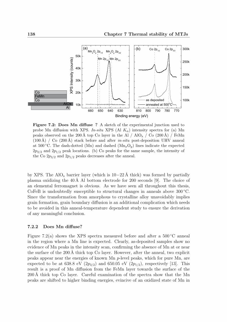
138 Chapter 7 Thermal stability of MTJs
CoFeMn
AlOxAl
Co
660 650 640 630
10k
20k
30k
40k
50k
(a) Co 2p1/2MnxOy 2p1/2
Co 2p3/2
MnxOy 2p3/2
Mn 2p1/2 Mn 2p3/2
XPS
Inte
nsity
(cou
nts)
Binding energy (eV)810 800 790 780 770
100k
150k
200k
250k
300k(b)
as deposited annealed at 500oC
Figure 7.2: Does Mn diffuse ? A sketch of the experimental junction used toprobe Mn diffusion with XPS. In-situ XPS (Al Kα) intensity spectra for (a) Mnpeaks observed on the 200 A top Co layer in the Al / AlOx / Co (200 A) / FeMn(100 A) / Co (200 A) stack before and after in-situ post-deposition UHV annealat 500 C. The dash-dotted (Mn) and dashed (MnxOy) lines indicate the expected2p3/2 and 2p1/2 peak locations. (b) Co peaks for the same sample, the intensity ofthe Co 2p3/2 and 2p1/2 peaks decreases after the anneal.
by XPS. The AlOx barrier layer (which is 10−22 A thick) was formed by partiallyplasma oxidizing the 40 A Al bottom electrode for 200 seconds [9]. The choice ofan elemental ferromagnet is obvious. As we have seen all throughout this thesis,CoFeB is undoubtedly susceptible to structural changes in anneals above 300 C.Since the transformation from amorphous to crystalline alloy unavoidably impliesgrain formation, grain boundary diffusion is an additional complication which needsto be avoided in this anneal-temperature dependent study to ensure the derivationof any meaningful conclusion.
7.2.2 Does Mn diffuse?
Figure 7.2(a) shows the XPS spectra measured before and after a 500 C annealin the region where a Mn line is expected. Clearly, as-deposited samples show noevidence of Mn peaks in the intensity scan, confirming the absence of Mn at or nearthe surface of the 200 A thick top Co layer. However, after the anneal, two explicitpeaks appear near the energies of known Mn p-level peaks, which for pure Mn, areexpected to be at 638.8 eV (2p3/2) and 650.05 eV (2p1/2), respectively [13]. Thisresult is a proof of Mn diffusion from the FeMn layer towards the surface of the200 A thick top Co layer. Careful examination of the spectra show that the Mnpeaks are shifted to higher binding energies, evincive of an oxidized state of Mn in

7.2 Experimental Results 139
670 660 650 640 630 620
10k
11k
20k
30k
40k
50k
60k
70k
0 150 300 450
0.0
0.1
0.2
0.3
0.4
XPS
Inte
nsity
(cou
nts) 100oC
200oC 300oC 400oC 500oC 500oC =70o
Binding Energy (eV)
MnMnO
Anneal temp. (oC)
Mn/
Co
inte
nsity
ra
tio (a
rb. u
.)
Figure 7.3: Mn diffusion as a function of anneal temperature. Mn intensityin each sample measured after an increasingly higher anneal temperature. Notethat the XPS intensity for measurements below an anneal temperature of 400 Cis plotted on a log scale. The diffused Mn oxidizes after reaching the surface ofthe top Co layer. This is clearly seen in the spectra measured at gracing angle(θ =70) after an anneal at 500 C which has visibly larger intensity as comparedto a corresponding measurement at normal incidence. Inset shows the Mn to Cointensity ratio measured in our XPS spectra as a function of post-deposition annealtemperature.
the Co layer. In our sample, the 2p3/2 Mn oxide peak is found to be around 641.4 eV.The literature values for the 2p3/2 peaks of various manganese oxides are found tolie between 641-642 eV [13, 15]. The formation of Mn oxide near the surface ofthe top Co layer is purely due to the background partial pressure of oxygen in thechamber, which is introduced by the degassing of adsorbed oxygen from the sampleplate during the anneal. Although we do not completely exclude the possibility ofoxygen driven Mn diffusion (reported for a 30 A thick CoFe layer by [11]) towardsthe surface of the top Co layer, we believe that our 200 A thick top and bottom Colayers should inhibit such a process.
Figure 7.1(b) shows the corresponding XPS spectra for Co 2p3/2 (778.1 eV) and2p1/2 (793.0 eV) peaks. It can be seen that the spectral intensity of peaks for the as-deposited sample is much larger than the annealed sample, confirming the decrease

140 Chapter 7 Thermal stability of MTJs
of Co concentration near the surface of the layer, due to its displacement by Mn.However, no oxidation of Co is evident, since there is no distinguishable shift in thepeaks. Co 2p3/2 peaks are expected at 778.1 eV, and those for its oxides are expectedbetween 779.8−780.2 eV [13, 15]. These results are in accordance with the fact thatthe (negative) free energy of formation is lowest for cobalt oxides, intermediate formanganese oxides and highest for aluminum oxides [14], making it difficult for Coto oxidize in the presence of Al and Mn.
Figure 7.3 shows the Mn spectra measured on different samples each annealed atprogressively higher temperatures. The influence of the anneal temperature in pro-moting Mn diffusion is clearly visible here. One notices a small bump appearing evenat an anneal at 200 C. As we have seen in Section 2.3.1, a gracing angle incidencemeasurement is more sensitive to the outermost surface layers. In Figure 7.3, thegracing angle incidence measurement (θ = 70) performed after an anneal at 500 Cshows a clear presence of Mn oxide on the surface layer, since the intensity of the Mnoxide peak is much larger than that observed in a corresponding measurement atnormal incidence. By fitting these peaks to gausssians one can obtain the Mn to Cospectral intensity ratio as a function of anneal temperature. The ratio is calculatedby removing the background in the measurements, fitting the peaks to expected Mnand Co peaks, and then deriving the area under the curve. This ratio is shown inthe inset of Figure 7.3. It is noteworthy that although the Mn/Co ratio at or nearthe surface of the 200 A top Co layer increases even after anneals at 200 C, it showsa definite kink around 300 C, which has been reported as the onset temperature forTMR collapse [5].
7.2.3 Influence of Mn diffusion on the TSP
To measure the effect of Mn diffusion on TSP, cross-striped tunnel junctions withand without FeMn were prepared similar to the XPS samples. A 60 A Ta cappinglayer was added on top. The junctions have an area of 400×400 µm2 and a resistance-area product of roughly 105 Ωµm2. STS measurements similar to those discussed inSection 2.5.1 were performed on these junctions. Figure 7.4(a) shows representativemeasurements for Al / AlOx / Co while Figure 7.4(b) corresponds to an Al / AlOx
/ Co90Fe10 junction at 0.26 K. The extracted TSP (38± 1%) for Co and (48± 1%)Co90Fe10 junctions are in fair agreement with earlier work [18].
Figure 7.4(c) shows TSP as a function of post-deposition anneal temperature forjunctions which do (closed symbols) and do not (open symbols) contain an FeMnlayer. Remarkably, TSP does not suffer any degradation in response to anneal up to500 C for both types of ferromagnets, independent of the presence of FeMn. Also,the absolute values of TSP for a particular ferromagnet does not change beforeand after the anneal, irrespective of Mn diffusion into the layers. This result is inqualitative agreement with the work of Kim and Moodera [19], who report that Mnconcentrations as high as 30% in Al / AlOx / CoyMn1−y junctions have only a weaknegative effect on the TSP. In addition, the anneals do not affect other junction

7.2 Experimental Results 141
0 150 300 4500
10
20
30
40
50
60
TSP (%)
(c) TSP
Co90Fe10
Co/FeMn
Co90Fe10/FeMn
Co
Anneal temperature (oC)-1.0 -0.5 0.0 0.5 1.0-1.0 -0.5 0.0 0.5 1.0
0.0
0.5
1.0
1.5
2.0
Ta=500 C
Nor
mal
ized
Con
duct
ance
TSP48%
(b) Co90Fe10
Bias Voltage (mV)
B = 0 T Fit B > 2.5 T Fit
(a) Co
TSP38%
Ta=500 C
Figure 7.4: Thermal stability of the TSP. Conductance of Al / AlOx / Co (a)and Al / AlOx / Co90Fe10 junction (b) at 0.26 K. The zero field curve (¤) showsthe Al superconducting gap while the >2.5T (©) curve reveals the TSP of CoFeBwhen fit (solid lines) with Maki theory [16]. (c) TSP measured after an in-situ 30minute post-deposition UHV anneal in Al / AlOx / Co and Al / AlOx / Co90Fe10
junctions which do (closed symbols) and do not (open symbols) contain an FeMnlayer. This data shows that TSP is not affected by the presence of an FeMn layeron top of the ferromagnet.
parameters such as junction resistance and the superconducting band gap of our Alelectrode. The thermal robustness of TSP above 300 C (evident in Figure 7.4) is insharp contrast with the effect of post-deposition annealing on the TMR of MTJ’s.In order to clarify this apparent contradiction further experiments are indispensable.
The stable TSP in our junctions suggest that the TMR degradation may not bedue to a degradation of the intrinsic TSP of the AlOx / Co or AlOx / Co90Fe10 sys-tem, but instead is a result of extrinsic influences, such as the diffusion of impurityatoms into the barrier or to one of its interfaces. It is notable that our junctions areannealed in UHV (base pressure 10−9 mbar), as compared to earlier work by Car-doso et al. and Lee et al. [5, 11, 12] who used vacuum chamber pressures of around10−6 mbar. We have already shown in junctions without FeMn, UHV anneals pre-serve the TSP as compared to similar junctions annealed in an Ar gas environment.This Ar environment was known to have a comparatively higher partial pressure ofother gaseous impurities like oxygen and nitrogen [4].
7.2.4 Impact of annealing on TSP
We now turn our attention to another interesting observation. Typically, annealsbelow 300 C enhances TMR. One explanation of this enhancement in TMR is animprovement of TSP due to migration of excess oxygen from the bottom ferro-

142 Chapter 7 Thermal stability of MTJs
magnetic electrode into the AlOx barrier [20]. This stoichiometric redistribution ofoxygen in the barrier results in a sharper interface and improved barrier properties.Consequently, the barrier height is expected to increase, and spin-independent tun-neling processes are expected to decrease, both leading to higher TMR. Anotherexplanation which concerns both electrodes, is the possibility of a change in theferromagnet structure at the interface after the anneal. However, our measurementsdo not show an increase in TSP when our junction stack is annealed at 100−300 C,which indicates that there is no change at the barrier-ferromagnet interface or inthe structure of the ferromagnetic electrode which contributes to enhancement ofTSP, and subsequently, TMR. Therefore, the second explanation, i.e., change in theferromagnetic electrode structure, is not supported by our measurements.
7.3 Summary
In summary, we investigated Mn diffusion in Al / AlOx / ferromagnet junctions andits effect on the TSP of the electrons tunneling from the ferromagnet. Contrary tothe current belief, we have shown that TSP in Al / AlOx / Co and Al / AlOx /Co90Fe10 junctions is thermally stable up to 500 C, despite of Mn diffusion towardsthe barrier-ferromagnet interface.

BIBLIOGRAPHY 143
Bibliography
[1] For example, with respect to industrial and automobile sensors, see the GermanBMBF project ”Magnetoelectronic” specifications led by Robert Bosch GmbH.7.1.1
[2] S. S. P. Parkin, K. P. Roche, M. G. Samant, P. M. Rice, R. B. Beyers,R. E. Scheuerlein, E. J. OSullivan, S. L. Brown, J. Bucchigano, D. W. Abra-ham, Y. Lu, M. Rooks, P. L. Trouilloud, R. A. Wanner, and W. J. Gallagher,Exchange-biased magnetic tunnel junctions and application to nonvolatile mag-netic random access memory (invited). J. Appl. Phys. 85, 5828 (1999). 7.1.1
[3] S. Tehrani, J. M. Slaughter, M. Deherrera, B. N. Engel, N. D. Rizzo, J. Salter,M. Durlam, R. W. Dave, J. Janesky, B. Butcher, K. Smith, and G. Grynkewich,Magnetoresistive random access memory using magnetic tunnel junctions. Proc.of the IEEE 91, 703 (2003). 7.1.1
[4] C. H. Kant, J. T. Kohlhepp, H. J. M. Swagten, and W. J. M. de Jonge, Intrinsicthermal robustness of tunneling spin polarization in Al/Al2O3/Co junctions.Appl. Phys. Lett. 84, 1141 (2004). 7.1.1, 7.1, 7.2.3
[5] S. Cardoso, P. P. Freitas, C. de Jesus, P. Wei, and J. C. Soares, Spin-tunnel-junction thermal stability and interface interdiffusion above 300C. Appl. Phys.Lett. 76, 610 (2000). 7.1.1, 7.1, 7.2.2, 7.2.3
[6] M. G. Samant, J. Luning, J. Stohr, and S. S. P. Parkin, Thermal stability ofIrMn and MnFe exchange-biased magnetic tunnel junctions. Appl. Phys. Lett.76, 3097 (2000). 7.1.1
[7] G. A. Prinz, Magnetoelectronics. Science 282, 1660 (1998).
[8] P. LeClair, J. T. Kohlhepp, H. J. M. Swagten, and W. J. M. de Jonge, Interfacialdensity of states in magnetic tunnel junctions. Phys. Rev. Lett. 86, 1066 (2001).7.1.2
[9] P. LeClair, J. T. Kohlhepp, A. A. Smits, H. J. M. Swagten, B. Koopmans, andW. J. M. de Jonge, Optical and in-situ characterization of plasma oxidized Alfor magnetic tunnel junctions. J. Appl. Phys. 87, 6070 (2000). 7.2.1
[10] R. Meservey and P. Tedrow, Spin-polarized electron tunneling. Phys. Rep. 238,173 (1994). 7.1.2
[11] C. S. Yoon, J. H. Lee, D. Jeong, C. K. Kim, J. H. Yuh, and R. Haasch, Diffusionstudy of the exchange-biased NiFe/MnIr/CoFe electrode in magnetic tunneljunctions. Appl. Phys. Lett. 80, 3976 (2002). 7.2.2, 7.2.3

144 Chapter 7 Thermal stability of MTJs
[12] J. H. Lee, D. Jeong, C. S. Yoon, C. K. Kim, B. G. Park, and T. D. Lee, Interdif-fusion in antiferromagnetic/ferromagnetic exchange coupled NiFe/IrMn/CoFemultilayer. J. Appl. Phys. 91, 1431 (2002). 7.2.3
[13] J. F. Moulder, W. F. Stickle, P. E. Sobol, and K. D. Bomben, Handbook of X-rayPhotoelectron Spectroscopy, Physical Electronics Division, second ed., (1995).7.2.2
[14] R. C. Weast, Handbook of Chemistry and Physics, p. D-61, CRC press, 55th
ed., (1975). 7.2.2
[15] D. Briggs, and M. P. Seah, eds. Practical surface analysis, 2nd edn. Wiley,Chichester. (1990). 7.2.2
[16] K. Maki, Pauli paramagnetism and superconducting state. II. Prog. Theor.Phys. 32, 29-36 (1964). 7.4
[17] R. Meservey, P. M. Tedrow, and R. C. Bruno, Tunneling measurements onspin-paired superconductors with spin-orbit scattering. Phys. Rev. B 11, 4224(1975).
[18] J. S. Moodera, J. Nassar, and G. Mathon, Spin-tunneling in ferromagneticjunctions. Annu. Rev. Mater. Sci. 29, 381 (1999). 7.2.3
[19] T. H. Kim and J. S. Moodera, Enhanced ferromagnetism and spin-polarizedtunneling studies in Co-Mn alloy films. Phys. Rev. B 66, 104436 (2002). 7.2.3
[20] R. C. Sousa, J. J. Sun, V. Soares, P. P. Freitas, A. Kling, M. F. da Silva,and J. C. Soares, Large tunneling magnetoresistance enhancement by thermalanneal. Appl. Phys. Lett. 73, 3288 (1998). 7.2.4
[21] P. V. Paluskar, C. H. Kant, J. T. Kohlhepp, A. T. Filip, H. J. M. Swagten,B. Koopmans, and W. J. M. de Jonge, Mn diffusion and the thermal stabilityof tunneling spin polarization. J. Appl. Phys. 97, 10C925 (2005). 1

145 Summary
Summary
Key concepts in spin tunneling
Amorphous ferromagnets for spintronics
This Ph.D. thesis is devoted to the fundamental understanding of the proper-ties of ternary CoFeB alloys, and to an endevour in exploring open questions inspin tunneling by employing these properties. These ternary alloys have gainedextreme importance in spintronic devices by showing large tunneling magnetoresis-tance (TMR) effects with AlOx and MgO based magnetic tunnel junctions (MTJs).
In view of this emerging impact of CoFeB in various spintronics applications wasobvious during the time of this thesis, so also was the necessity for a thorough ex-perimental and theoretical analysis of its atomic and electronic structure and theircombined impact on its tunneling spin polarization (P or TSP). To the first order,the TSP is representative of the inequality in the number of spin-up and spin-downconduction electrons at the Fermi level, and is the fundamental parameter in mostspintronic devices. Returning to CoFeB, apart from a few of its bulk magnetic prop-erties studied in the 1980’s every other structural, magnetic and electronic aspectof these alloys remained unexplored, especially in thin films relevant to spintronics.Moreover, the realization that these as-deposited amorphous alloys undergo a radi-cal structural transition (crystallization) after an anneal also opens up possibilitiesto explore issues in spin tunneling which remain hitherto unaddressed.
In Chapter 1 of this thesis we portrayed a few contemporary notions regardingspin tunneling and described crucial materials, experiments, and results on suchtunnel junctions. In Chapter 2, we looked at device fabrication methods and thevarious experimental analysis tools used in this thesis. Here, to exemplify the varioustechniques, a few experimental results relevant to later chapters were also presented.In particular, we described some unpublished work reporting (i) large exchange biasfields obtained for CoFeB alloys, (ii) and the development of a CIPT set-up usingwhich we demonstrated CIPT-TMR in AlOx based MTJs and characterization ofMgO and NiO barriers. In Chapter 3, we investigated some structural aspects ofCoFeB alloys. We showed that as-deposited films grow amorphous and investigatethe influence of crystallization of these amorphous alloys on their structural andmagnetic properties after a single anneal. MOKE and XRD measurement showedthat the films crystallized gradually with increasing temperature
In Chapter 4, we investigated the atomic and electronic structure of a singleCoFeB composition. We aimed to address two issues:(i) an issue which had never been investigated experimentally or computationallyto date was addressed – namely – the TSP of an amorphous ferromagnet. We in-

Summary 146
vestigated why these ferromagnets exhibit such high TMR values in the first placeand how one can quantitatively describe the TSP of a ternary amorphous alloy inconjunction to an amorphous barrier.(ii) we explored the correlation between ferromagnet morphology, its electronic struc-ture and their combined impact on TSP. In other words, we investigated how a dis-tinct and major structural alteration of the ferromagnetic electrode at the interfacewith the barrier influences the TSP.
We showed that amorphous Co72Fe20B8 shows a considerably large TSP of 53%,and contrary to one’s primary intuition, this TSP value was found to be largerthan that observed for fcc CoFeB. First-principles atomic structure calculationsshowed good agreement with extended x-ray absorption fine structure measurementson amorphous CoFeB. Remarkably, both for amorphous and fcc CoFeB, electronicstructure calculations based on the calculated atomic structure exhibited a conspic-uous agreement between the spin polarization of the s-electron density of states andexperimentally measured TSP. We emphasize that such a quantitative agreementbetween theory and experiment for a complex amorphous / crystalline ternary alloyhas never been reported before.
Moreover, the first principles calculations also revealed that the B sp-states werehighly spin polarized and made a significant contribution to the alloy spin polariza-tion. We believe that this aspect too is of significant relevance to spin-torque basedMTJs and nanowires, as well as conventional MTJs employing CoFeB alloys.
In Chapter 5, we probed some aspects of inelastic tunneling of electrons whena sharp contrast – structural change from amorphous to crystalline electrode – wasinduced at the barrier-ferromagnet interface. In particular, the changes in the lowenergy magnetic excitations induced by inelastically tunneling electrons were investi-gated. For amorphous CoFeB at the interface, we saw indications of size quantizationof the magnons. For fcc CoFeB at the interface, we saw distinct excitations around10 mV which could also be related to magnon-assisted spin flip tunneling. Withthese observations, we demonstrated that IETS is a powerful tool to investigate theimpact of interface structure changes in MTJs.
In Chapter 6, we probed the correlation between magnetism and TSP in CoFeBalloys. Such a correlation had been an outstanding issue in spin tunneling sinceits first observation in 1976. We found that the amorphous CoFeB alloys are verysuitable to address this issue. Our measurements showed that the alloy magneticmoment as well as the s-electron dominated TSP showed the Slater-Pauling behav-ior. XMCD measurements which probe the properties of d -electrons by synchrotronradiations show a crossover from weak to strong ferromagnetism in the Fe-DOS. Tothe best of our knowledge, this is the first observation of the Slater-Pauling behaviorin transition metal alloys using the XMCD technique. We conclude that this mag-netic crossover in the Fe-DOS, together with s-d hybridization, provides an intuitiveunderstanding of the direct correlation between the magnetic moment and TSP. Wealso believe that the tunable electronic and magnetic properties of these CoFeB

147 Summary
alloys allow access to engineer and advance the application potential of spintronicdevices.
Finally, in Chapter 7, we investigated the thermal stability of MTJs and theeffect of high-temperature annealing. Specifically, the role of Mn diffusion from theantiferromagnets used to exchange bias one of the ferromagnetic layers was probed.We find that though Mn diffuses after annealing, it did not influence the TSP.

List of publications 148
List of publications
Magnetic tunnel junctionsH.J.M. Swagten and P.V. PaluskarEncyclopedia of Material Science and Technology, in press.
Spin tunneling in junctions with disordered ferromagnetsP.V. Paluskar, J.J. Attema, G.A. de Wijs, S. Fiddy, E. Snoeck,J.T. Kohlhepp, H.J.M. Swagten, R.A. de Groot, and B. KoopmansPhysical Review Letters, 100, 052705 (2008).
Impact of interface crystallization on inelastic tunneling in Al / AlOx / CoFeBP.V. Paluskar, F.L. Bloom, E. Snoeck, J.T. Kohlhepp, H.J.M. Swagten,and B. KoopmansApplied Physics Letters, 91, 222501 (2007).
Correlation between magnetism and tunneling spin polarizationP.V. Paluskar, R. Lavrijsen, M. Sicot, J.T. Kohlhepp, H.J.M. Swagten,and B. KoopmansSubmitted.
Controlling speed and efficiency of ultrafast demagnetization by direct transferof spin angular momentumG. Malinowski, F. Dalla Longa, J.H.H. Rietjens, P.V. Paluskar, R. Huijink,H.J.M. Swagten, and B. KoopmansSubmitted.
Tunneling spin polarization and annealing of Co72Fe20B8
H.J.M. Swagten, P.V. Paluskar, R. Lavrijsen, J.T. Kohlhepp, and B. KoopmansJournal of Magnetism and Magnetic Material 310, 2012 (2007).
Influence of interface structure on the tunnelling spin polarization of CoFeB alloysP.V. Paluskar, J.T. Kohlhepp, H.J.M. Swagten, B. Koopmans, R. Wolters,H. Boeve, and E. SnoeckJournal of Physics D: Applied Physics 40, 1234 (2007).

149 List of publications
Co72Fe20B8: Structure, magnetism, and tunneling spin polarizationP.V. Paluskar, J.T. Kohlhepp, H.J.M. Swagten, and B. KoopmansJournal of Applied Physics 99, 08E503 (2006).
Mn diffusion and the thermal stability of tunneling spin polarizationP.V. Paluskar, C.H. Kant, J.T. Kohlhepp, A.T. Filip, H.J.M. Swagten,B. Koopmans and W.J.M. de JongeJournal of Applied Physics 97, 10C925 (2005).
Thermal stability of tunneling spin polarizationC.H. Kant, J.T. Kohlhepp, P.V. Paluskar, H.J.M. Swagten and W.J.M. de JongeJournal of Magnetism and Magnetic Materials 286, 154 (2004).

About the author 150
About the author
Paresh Vijay Paluskar
October 2, 1978 Born in Pandharpur, in the province Maharashtra, in India
1983 - 1994 Elementary Education, Mumbai
1994 - 1997 Diploma in InstrumentationBoard of Technical Education, Mumbai
1997 - 2000 Bachelor of Engineering, InstrumentationDr. Babasaheb Ambedkar Marathwada University, Aurangabad
2001 - 2003 Master of Science, Sensory Systems TechnologyFachhochschule Karlsruhe, Germany
Graduate work in the field of giant magnetoresistance and exchangebiasing at the research headquarters of Robert Bosch GmbHSchillerhohe, Stuttgart, Germany.“Imprinting of different pinning directions in a PtMnand synthetic antiferromagnet based spin valve 360 anglesensor using a current pulse and showing giant magnetoresistance.”
2003 - 2004 Courses in PhysicsEindhoven University of Technology, the NetherlandsUniversity of Bielefeld, Germany
2004 - 2008 Ph.D. candidateDepartment of Applied Physics,Eindhoven University of Technology, the NetherlandsResearch carried out in the group Physics of Nanostructures“Key concepts in spin tunneling:amorphous ferromagnets for spintronics”

151 Acknowledgements
Acknowledgements
It is a genuine pleasure to express my gratitude towards the individuals who sup-ported and motivated me during this work. To begin with, I am immensely indebtedto my promoters Bert Koopmans and Henk Swagten for their constant encourage-ment and persistent support, for believing in my abilities right from the beginningand giving me an opportunity to work, for tolerating my manifold idiosyncrasies,and for their generous friendship over the years. Bert has been a patient and kindmentor who has instilled the essential aspects of a good researcher in me. I havelearned greatly from his straightforward approach to research. My need for having ascientific (and at times un-scientific) conversation has always found an open door toHenk’s office. I have enormously enjoyed his company and good humor at many aconference and learned considerably from his ability to ask the most relevant ques-tions. Without Henk’s and Bert’s efforts, all of my scientific writing would read halfas well. I am also indebted to Bert and Henk for making me a part of the researchgroup where they have created a wonderful, informal research environment. Myday-to-day experiences in this environment have been the absolute highlight of mystay in Eindhoven. Due credit for this environment and my chance of working init also goes to Wim de Jonge. His urge to do worthwhile research, encouraging aconstant check on the relevance to the bigger picture, has hopefully rubbed off onme. I am grateful for his comments and input during this work. I would also like tothank Jurgen Kohlhepp, my co-promoter, for his support, humor, sarcasm, effort onthe photoemission measurements and annealing, and tireless and seemingly uncannyway of encouraging me in my work. I learned a great deal from his knowledge onx-ray photoemission, thin film growth, and exchange biasing.
I am extremely grateful to Gilles de Wijs, Jisk Attema, and Rob de Groot (Rad-boud University Nijmegen) for their unwavering support, and for their ingenuityand hardwork which resulted in a exceedingly fruitful collaboration. I thoroughlyenjoyed the long phone conversations with Gilles and Jisk, the never-ending dataexchange, the constant need for further discussion on the calculated results, andmy visits to Nijmegen. I sincerely appreciate the patience they have afforded meover these years. I would like to thank Rob for immediately realizing and undertak-ing the research project we envisioned. Without the resolved commitment of thesethree individuals to the collaboration, this work would not have been complete. Iwould also like to thank Etienne Snoeck (CEMES-CNRS, France) for the HRTEMmeasurements and for a fruitful collaboration. These measurements proved indis-

Acknowledgements 152
pensable to this thesis. A word of thanks to Steven Fiddy (Daresbury Labs, UK) forperforming and analyzing the EXAFS measurements with me which resulted in asignificant endorsement to the amorphous structure calculations of Gilles and Jisk.A word of appreciation to Hans Boeve and Rob Wolters (Philips Research Labs) fortheir collaboration on the resistivity measurements. A word of thanks to ReinderCoehoorn (Philips Research Labs) for making available his computational work onFeB systems, and for fruitful discussions.
My genuine thanks and appreciation to Corne Kant who introduced me to thedeposition and measurement equipment, and who built the SPT set-up extensivelyused in this work. El Corno’s ever-joyful attitude, his open-minded friendship,generosity, liking of spicy Indian food, and love affair with the local dance club’liquid’ were a veritable experience to share. I also extend my appreciation to theMaster (Rein and Roeland) and Bachelor (Coen and Peter) students who workedwith me on a variety of projects. I completely enjoyed working with them, guidingthem, learning from them the trade secrets of their own research work, and theirgood friendship. Their zealous attitude towards their experiments, creativity, andexperimental acuity were contagious.
Many thanks to Oleg for his kind friendship and encouragement. I fully enjoyedour outings together in Belgium, and the discussions we had at late hours whileperforming our individual experiments. I had the good fortune to work with manyphd’s and post-docs during my stay in Eindhoven. Exercising the freedom of ex-pression with these good souls in the coffee room, or sharing a ping-pong game, adinner table, a drink, an extremely dangerous explosion in the lab, a game of cards,some surprisingly common grievances from daily life, has been a privilege and oneof my favoriet pastime. In no particular order, many thanks to the clan consistingof Jeroen, Harm, Czaba, Coen, Andrei, Jurgen, Francesco, Sabine, Greg, Muriel,Wiebe, and Corine. Not only did all these people manage to put a smile on my faceevery single day, but also they created a homely environment where I could affordto be myself. For all these aspects of my daily life in Eindhoven, I am singularlyindebted to each and every one of them. A note of deep appreciation to my office-mates Francisco and Omer. Thanks to their sense of humor, their appreciation ofmy peculiar sense of humor, their patience with my numerous phone conversationsto India, and their own tiny eccentricities, we shared innumerable laughs together,and earned the honor of being the noisiest office on the floor. Some of the afore-mentioned individuals (Corne, Rein, Muriel, Roeland, Francisco, Greg, Andrei) alsocollaborated with me on some projects. Many thanks for the good work we didtogether. Rein and Muriel deserve a special mention, as they suffered and tolerateda sleep-deprived Paresh when they themselves were sleepless on our long guards atthe synchrotrons.
Many thanks to our non-scientific and technical staff consisting of Karin, Gerrie,Jeroen, and Jef. Their excellent work gave much needed support. Their superbsense of humor, their open-mindedness, their efforts for arranging numerous group

153 Acknowledgements
activities like borrels, group-outings, parties which I immensely enjoyed.....all de-serve my gratefulness. Karin, our beloved secretary, deserves a special mention fortaking care of all my office related issues, for organizing all of my trips, and forgenuinely covering-up for my lack of organizational skills. I would also like to thankPeter Bobbert for giving his lecture ‘quantum theory of solids’ in English at suchshort notice.
A word of thanks to Onkar Ambekar, my friend of many years, and to my friendSiddhartha Dhar for their friendship, their support, their encouragement, and theirhelp in maintaining my sanity.
Most importantly, I would like to thank my family. As I mentioned in the firstfew pages, this thesis is dedicated to them. I am forever indebted to my parents,Prabha and Vijay Paluskar, and my younger brother Parag for their unconditionallove and relentless support. And I am eternally indebted to my wife, Sonu, my bestfriend and soul-mate for the past decade, my beacon, and the light in my heart. Hersupport, sacrifices, resolve, belief in me, sense of responsibility....I am out of wordsto describe what she means to me and to this work.