product technical specification & customer design ... technical specification & customer...
TRANSCRIPT

Product Technical Specification & Customer Design Guidelines
AirPrime SL808X
2400058Rev 1

Preface
Important Notice
Due to the nature of wireless communications, transmission and reception of data can never be guaranteed. Data may be delayed, corrupted (i.e., have errors) or be totally lost. Although significant delays or losses of data are rare when wireless devices such as the Sierra Wireless modem are used in a normal manner with a well-constructed network, the Sierra Wireless modem should not be used in situations where failure to transmit or receive data could result in damage of any kind to the user or any other party, including but not limited to personal injury, death, or loss of property. Sierra Wireless accepts no responsibility for damages of any kind resulting from delays or errors in data transmitted or received using the Sierra Wireless modem, or for failure of the Sierra Wireless modem to transmit or receive such data.
Safety and Hazards
Do not operate the Sierra Wireless modem in areas where blasting is in progress, where explosive atmospheres may be present, near medical equipment, near life support equipment, or any equipment which may be susceptible to any form of radio interference. In such areas, the Sierra Wireless modem MUST BE POWERED OFF. The Sierra Wireless modem can transmit signals that could interfere with this equipment.
Do not operate the Sierra Wireless modem in any aircraft, whether the aircraft is on the ground or in flight. In aircraft, the Sierra Wireless modem MUST BE POWERED OFF. When operating, the Sierra Wireless modem can transmit signals that could interfere with various onboard systems.
Note: Some airlines may permit the use of cellular phones while the aircraft is on the ground and the door is open. Sierra Wireless modems may be used at this time.
The driver or operator of any vehicle should not operate the Sierra Wireless modem while in control of a vehicle. Doing so will detract from the driver or operator's control and operation of that vehicle. In some states and provinces, operating such communications devices while in control of a vehicle is an offence.
Limitation of Liability
The information in this manual is subject to change without notice and does not represent a commitment on the part of Sierra Wireless. SIERRA WIRELESS AND ITS AFFILIATES SPECIFICALLY DISCLAIM LIABILITY FOR ANY AND ALL DIRECT, INDIRECT, SPECIAL, GENERAL, INCIDENTAL, CONSEQUENTIAL, PUNITIVE OR EXEMPLARY DAMAGES INCLUDING, BUT NOT LIMITED TO, LOSS OF PROFITS OR REVENUE OR ANTICIPATED PROFITS OR REVENUE ARISING OUT OF THE USE OR INABILITY TO USE ANY SIERRA WIRELESS PRODUCT, EVEN IF SIERRA WIRELESS AND/OR ITS AFFILIATES HAS BEEN ADVISED OF THE POSSIBILITY OF SUCH DAMAGES OR THEY ARE FORESEEABLE OR FOR CLAIMS BY ANY THIRD PARTY.
Notwithstanding the foregoing, in no event shall Sierra Wireless and/or its affiliates aggregate liability arising under or in connection with the Sierra Wireless product, regardless of the number of events, occurrences, or claims giving rise to liability, be in excess of the price paid by the purchaser for the Sierra Wireless product.
Rev 1 Dec.10 Proprietary and Confidential - Specifications subject to change 3
Product Technical Specification & Customer Design Guidelines
Patents This product may contain technology developed by or for Sierra Wireless Inc.
This product includes technology licensed from QUALCOMM® 3G.
This product is manufactured or sold by Sierra Wireless Inc. or its affiliates under one or more patents licensed from InterDigital Group.
Copyright ©2010 Sierra Wireless. All rights reserved.
Trademarks AirCard® and Watcher® are registered trademarks of Sierra Wireless. Sierra Wireless, AirPrime and the Sierra Wireless logo are trademarks of Sierra Wireless.
Windows® and Windows Vista® are registered trademarks of Microsoft Corporation.
QUALCOMM® is a registered trademark of QUALCOMM Incorporated. Used under license.
Other trademarks are the property of their respective owners.
Contact Information
Consult our website for up-to-date product descriptions, documentation, application notes, firmware upgrades, troubleshooting tips, and press releases:
www.sierrawireless.com
Revision History
Sales Desk: Phone: 1-604-232-1488
Hours: 8:00 AM to 5:00 PM Pacific Time
E-mail: [email protected]
Post: Sierra Wireless13811 Wireless WayRichmond, BCCanada V6V 3A4
Fax: 1-604-231-1109
Web: www.sierrawireless.com
Revision number
Release date Changes
1 December 2010 Created document
4 Proprietary and Confidential - Specifications subject to change 2400058
Rev 1 Dec
Contents
Introduction . . . . . . . . . . . . . . . . . . . . . . . . . . . . . . . . . . . . . . . . . . . . . . . . . . . .15
General features. . . . . . . . . . . . . . . . . . . . . . . . . . . . . . . . . . . . . . . . . . . . . . 15
Support features. . . . . . . . . . . . . . . . . . . . . . . . . . . . . . . . . . . . . . . . . . . . . . 19
Support tools . . . . . . . . . . . . . . . . . . . . . . . . . . . . . . . . . . . . . . . . . . . . . . . . 19
Accessories . . . . . . . . . . . . . . . . . . . . . . . . . . . . . . . . . . . . . . . . . . . . . . . . . 20
Hardware development components . . . . . . . . . . . . . . . . . . . . . . . . . . . . . . 20
Ordering information. . . . . . . . . . . . . . . . . . . . . . . . . . . . . . . . . . . . . . . . . . . 20
Environmental issues . . . . . . . . . . . . . . . . . . . . . . . . . . . . . . . . . . . . . . . . . . 20
RoHS directive compliant . . . . . . . . . . . . . . . . . . . . . . . . . . . . . . . . . . . . .20
Disposing of the product . . . . . . . . . . . . . . . . . . . . . . . . . . . . . . . . . . . . .21
Functional Specifications . . . . . . . . . . . . . . . . . . . . . . . . . . . . . . . . . . . . . . . .23
Functional architecture . . . . . . . . . . . . . . . . . . . . . . . . . . . . . . . . . . . . . . . . . 23
Chipsets . . . . . . . . . . . . . . . . . . . . . . . . . . . . . . . . . . . . . . . . . . . . . . . . . .23
Extended AT commands . . . . . . . . . . . . . . . . . . . . . . . . . . . . . . . . . . . . . . . 23
Technical Specifications . . . . . . . . . . . . . . . . . . . . . . . . . . . . . . . . . . . . . . . . .25
Power supply . . . . . . . . . . . . . . . . . . . . . . . . . . . . . . . . . . . . . . . . . . . . . . . . 25
Burst transmission current requirements . . . . . . . . . . . . . . . . . . . . . . . . .26
Power input (VCC_3V6) . . . . . . . . . . . . . . . . . . . . . . . . . . . . . . . . . . . . . .26
Start-up current . . . . . . . . . . . . . . . . . . . . . . . . . . . . . . . . . . . . . . . . . . . .26
Ground connection. . . . . . . . . . . . . . . . . . . . . . . . . . . . . . . . . . . . . . . . . . . . 27
Decoupling of power supply signals . . . . . . . . . . . . . . . . . . . . . . . . . . . . . . . 27
Mechanical specifications. . . . . . . . . . . . . . . . . . . . . . . . . . . . . . . . . . . . . . . 27
Mechanical illustrations . . . . . . . . . . . . . . . . . . . . . . . . . . . . . . . . . . . . . .28
Labeling . . . . . . . . . . . . . . . . . . . . . . . . . . . . . . . . . . . . . . . . . . . . . . . . . . . . 29
Embedded SIM (eSIM). . . . . . . . . . . . . . . . . . . . . . . . . . . . . . . . . . . . . . . . . 29
Thermal considerations . . . . . . . . . . . . . . . . . . . . . . . . . . . . . . . . . . . . . . . . 30
SED (Smart Error Detection) . . . . . . . . . . . . . . . . . . . . . . . . . . . . . . . . . . . . 30
.10 Proprietary and Confidential - Specifications subject to change 5
Product Technical Specification & Customer Design Guidelines
6
Firmware upgrade . . . . . . . . . . . . . . . . . . . . . . . . . . . . . . . . . . . . . . . . . . . . 30
Interfaces . . . . . . . . . . . . . . . . . . . . . . . . . . . . . . . . . . . . . . . . . . . . . . . . . . . . . 31
System design . . . . . . . . . . . . . . . . . . . . . . . . . . . . . . . . . . . . . . . . . . . . . . . 31
Pin configuration . . . . . . . . . . . . . . . . . . . . . . . . . . . . . . . . . . . . . . . . . . . 33
Pin description . . . . . . . . . . . . . . . . . . . . . . . . . . . . . . . . . . . . . . . . . . . . . 34
Digital I/O electrical information . . . . . . . . . . . . . . . . . . . . . . . . . . . . . . . . . . 39
Electrical characteristics . . . . . . . . . . . . . . . . . . . . . . . . . . . . . . . . . . . . . 39
Signal reset states . . . . . . . . . . . . . . . . . . . . . . . . . . . . . . . . . . . . . . . . . . 40
Reference schematic . . . . . . . . . . . . . . . . . . . . . . . . . . . . . . . . . . . . . . . . . . 40
General purpose input/output . . . . . . . . . . . . . . . . . . . . . . . . . . . . . . . . . . . 40
Pin descriptions . . . . . . . . . . . . . . . . . . . . . . . . . . . . . . . . . . . . . . . . . . . . 41
Main serial link (UART1) . . . . . . . . . . . . . . . . . . . . . . . . . . . . . . . . . . . . . . . 41
UART1 pin descriptions . . . . . . . . . . . . . . . . . . . . . . . . . . . . . . . . . . . . . . 42
Interface implementation . . . . . . . . . . . . . . . . . . . . . . . . . . . . . . . . . . . . . 42
SIM interface . . . . . . . . . . . . . . . . . . . . . . . . . . . . . . . . . . . . . . . . . . . . . . . . 42
SIM pin descriptions . . . . . . . . . . . . . . . . . . . . . . . . . . . . . . . . . . . . . . . . 43
Application notes . . . . . . . . . . . . . . . . . . . . . . . . . . . . . . . . . . . . . . . . . . . 43
USB 2.0 interface. . . . . . . . . . . . . . . . . . . . . . . . . . . . . . . . . . . . . . . . . . . . . 44
USB pin descriptions . . . . . . . . . . . . . . . . . . . . . . . . . . . . . . . . . . . . . . . . 45
Electrical characteristics . . . . . . . . . . . . . . . . . . . . . . . . . . . . . . . . . . . . . 45
Application notes . . . . . . . . . . . . . . . . . . . . . . . . . . . . . . . . . . . . . . . . . . . 45
Host-developed USB drivers . . . . . . . . . . . . . . . . . . . . . . . . . . . . . . . . . . 45
USB Suspend mode . . . . . . . . . . . . . . . . . . . . . . . . . . . . . . . . . . . . . . . . 46
USB Resume mode . . . . . . . . . . . . . . . . . . . . . . . . . . . . . . . . . . . . . . . . . 46
RF interface . . . . . . . . . . . . . . . . . . . . . . . . . . . . . . . . . . . . . . . . . . . . . . . . . 47
RF connections . . . . . . . . . . . . . . . . . . . . . . . . . . . . . . . . . . . . . . . . . . . . 47
RF pin descriptions . . . . . . . . . . . . . . . . . . . . . . . . . . . . . . . . . . . . . . . . . 48
RF performance . . . . . . . . . . . . . . . . . . . . . . . . . . . . . . . . . . . . . . . . . . . 48
Antenna specifications . . . . . . . . . . . . . . . . . . . . . . . . . . . . . . . . . . . . . . 50
Radiated emissions . . . . . . . . . . . . . . . . . . . . . . . . . . . . . . . . . . . . . . . . . 51
Radiated sensitivity measurement . . . . . . . . . . . . . . . . . . . . . . . . . . . . . 51
Audio interfaces. . . . . . . . . . . . . . . . . . . . . . . . . . . . . . . . . . . . . . . . . . . . . . 51
Proprietary and Confidential - Specifications subject to change 2400058
Contents
Rev 1 Dec
Analog audio interface . . . . . . . . . . . . . . . . . . . . . . . . . . . . . . . . . . . . . . . . . 52
Pin descriptions . . . . . . . . . . . . . . . . . . . . . . . . . . . . . . . . . . . . . . . . . . . .52
Microphone features . . . . . . . . . . . . . . . . . . . . . . . . . . . . . . . . . . . . . . . .52
Speaker features . . . . . . . . . . . . . . . . . . . . . . . . . . . . . . . . . . . . . . . . . . .57
Supported voice features . . . . . . . . . . . . . . . . . . . . . . . . . . . . . . . . . . . . .60
Short Message Service (SMS) . . . . . . . . . . . . . . . . . . . . . . . . . . . . . . . . .61
UMTS radio access bearers supported . . . . . . . . . . . . . . . . . . . . . . . . . .61
Digital audio interface (PCM) . . . . . . . . . . . . . . . . . . . . . . . . . . . . . . . . . . . . 62
PCM pin descriptions . . . . . . . . . . . . . . . . . . . . . . . . . . . . . . . . . . . . . . . .62
PCM waveforms . . . . . . . . . . . . . . . . . . . . . . . . . . . . . . . . . . . . . . . . . . . .63
JTAG interface . . . . . . . . . . . . . . . . . . . . . . . . . . . . . . . . . . . . . . . . . . . . . . . 64
Signals and Indicators . . . . . . . . . . . . . . . . . . . . . . . . . . . . . . . . . . . . . . . . . . .65
Overview . . . . . . . . . . . . . . . . . . . . . . . . . . . . . . . . . . . . . . . . . . . . . . . . . . . 65
Power on/off signal (POWER_ON_N) . . . . . . . . . . . . . . . . . . . . . . . . . . . . . 66
Pin descriptions . . . . . . . . . . . . . . . . . . . . . . . . . . . . . . . . . . . . . . . . . . . .66
Electrical characteristics . . . . . . . . . . . . . . . . . . . . . . . . . . . . . . . . . . . . .66
Application notes . . . . . . . . . . . . . . . . . . . . . . . . . . . . . . . . . . . . . . . . . . .66
Reset Signal (SYSTEM_RESET_N) . . . . . . . . . . . . . . . . . . . . . . . . . . . . . . 68
Pin descriptions . . . . . . . . . . . . . . . . . . . . . . . . . . . . . . . . . . . . . . . . . . . .68
Electrical characteristics . . . . . . . . . . . . . . . . . . . . . . . . . . . . . . . . . . . . .68
Application notes . . . . . . . . . . . . . . . . . . . . . . . . . . . . . . . . . . . . . . . . . . .69
Wake signal (WAKE_N) . . . . . . . . . . . . . . . . . . . . . . . . . . . . . . . . . . . . . . . . 70
Pin descriptions . . . . . . . . . . . . . . . . . . . . . . . . . . . . . . . . . . . . . . . . . . . .70
Electrical characteristics . . . . . . . . . . . . . . . . . . . . . . . . . . . . . . . . . . . . .70
Disable signal (W_DISABLE_N) . . . . . . . . . . . . . . . . . . . . . . . . . . . . . . . . . 71
Pin descriptions . . . . . . . . . . . . . . . . . . . . . . . . . . . . . . . . . . . . . . . . . . . .71
Electrical characteristics . . . . . . . . . . . . . . . . . . . . . . . . . . . . . . . . . . . . .71
Application notes . . . . . . . . . . . . . . . . . . . . . . . . . . . . . . . . . . . . . . . . . . .71
Buzzer output (BUZZER_EN) . . . . . . . . . . . . . . . . . . . . . . . . . . . . . . . . . . . 72
Pin descriptions . . . . . . . . . . . . . . . . . . . . . . . . . . . . . . . . . . . . . . . . . . . .72
Electrical characteristics . . . . . . . . . . . . . . . . . . . . . . . . . . . . . . . . . . . . .72
.10 Proprietary and Confidential - Specifications subject to change 7
Product Technical Specification & Customer Design Guidelines
8
Flash LED (LED_FLASH) . . . . . . . . . . . . . . . . . . . . . . . . . . . . . . . . . . . . . . 73
Pin descriptions . . . . . . . . . . . . . . . . . . . . . . . . . . . . . . . . . . . . . . . . . . . . 73
Electrical characteristics . . . . . . . . . . . . . . . . . . . . . . . . . . . . . . . . . . . . . 73
Power rail (VREF_1V8) . . . . . . . . . . . . . . . . . . . . . . . . . . . . . . . . . . . . . . . . 74
Pin descriptions . . . . . . . . . . . . . . . . . . . . . . . . . . . . . . . . . . . . . . . . . . . . 74
Electrical characteristics . . . . . . . . . . . . . . . . . . . . . . . . . . . . . . . . . . . . . 75
Application notes . . . . . . . . . . . . . . . . . . . . . . . . . . . . . . . . . . . . . . . . . . . 75
Reserved . . . . . . . . . . . . . . . . . . . . . . . . . . . . . . . . . . . . . . . . . . . . . . . . . . . 75
Power Consumption . . . . . . . . . . . . . . . . . . . . . . . . . . . . . . . . . . . . . . . . . . . . 77
Power states . . . . . . . . . . . . . . . . . . . . . . . . . . . . . . . . . . . . . . . . . . . . . . . . 79
Power state transitions . . . . . . . . . . . . . . . . . . . . . . . . . . . . . . . . . . . . . . 80
Network technology specifications . . . . . . . . . . . . . . . . . . . . . . . . . . . . . . . . 83
UMTS WCDMA FDD specifications. . . . . . . . . . . . . . . . . . . . . . . . . . . . . . . 83
Supported specifications . . . . . . . . . . . . . . . . . . . . . . . . . . . . . . . . . . . . . . . 85
UMTS (WCDMA) / GSM specifications . . . . . . . . . . . . . . . . . . . . . . . . . . . . 91
Design Guidelines . . . . . . . . . . . . . . . . . . . . . . . . . . . . . . . . . . . . . . . . . . . . . . 95
General rules and constraints . . . . . . . . . . . . . . . . . . . . . . . . . . . . . . . . . . . 95
PCB layout recommendations . . . . . . . . . . . . . . . . . . . . . . . . . . . . . . . . . . . 95
Power supply . . . . . . . . . . . . . . . . . . . . . . . . . . . . . . . . . . . . . . . . . . . . . . . . 95
Antenna . . . . . . . . . . . . . . . . . . . . . . . . . . . . . . . . . . . . . . . . . . . . . . . . . . . . 96
PCB specifications for the application board . . . . . . . . . . . . . . . . . . . . . . . . 96
Recommended PCB landing pattern . . . . . . . . . . . . . . . . . . . . . . . . . . . . . . 96
Routing constraints . . . . . . . . . . . . . . . . . . . . . . . . . . . . . . . . . . . . . . . . . . . 97
Power supply . . . . . . . . . . . . . . . . . . . . . . . . . . . . . . . . . . . . . . . . . . . . . . 97
SIM interface . . . . . . . . . . . . . . . . . . . . . . . . . . . . . . . . . . . . . . . . . . . . . . 98
Audio circuit . . . . . . . . . . . . . . . . . . . . . . . . . . . . . . . . . . . . . . . . . . . . . . . 98
RF circuit . . . . . . . . . . . . . . . . . . . . . . . . . . . . . . . . . . . . . . . . . . . . . . . . . 98
EMC and ESD recommendations . . . . . . . . . . . . . . . . . . . . . . . . . . . . . . . 100
Mechanical integration. . . . . . . . . . . . . . . . . . . . . . . . . . . . . . . . . . . . . . . . 101
Proprietary and Confidential - Specifications subject to change 2400058
Contents
Rev 1 Dec
Operating system upgrade. . . . . . . . . . . . . . . . . . . . . . . . . . . . . . . . . . . . . 101
Embedded Testability . . . . . . . . . . . . . . . . . . . . . . . . . . . . . . . . . . . . . . . . . . .103
Testing assistance provided by Sierra Wireless. . . . . . . . . . . . . . . . . . . . . 103
Integration requirements . . . . . . . . . . . . . . . . . . . . . . . . . . . . . . . . . . . . . . 103
IOT/Operator . . . . . . . . . . . . . . . . . . . . . . . . . . . . . . . . . . . . . . . . . . . . . . . 103
Module testing recommendations . . . . . . . . . . . . . . . . . . . . . . . . . . . . . . . 104
Serial link access . . . . . . . . . . . . . . . . . . . . . . . . . . . . . . . . . . . . . . . . . . . . 104
RF output accessibility . . . . . . . . . . . . . . . . . . . . . . . . . . . . . . . . . . . . . . . . 105
Certification Compliance and Recommended Standards . . . . . . . . . . . . . .107
UMTS compliance acceptance and certification . . . . . . . . . . . . . . . . . . . . 107
Certification compliance . . . . . . . . . . . . . . . . . . . . . . . . . . . . . . . . . . . . . . . 107
Applicable standards listing . . . . . . . . . . . . . . . . . . . . . . . . . . . . . . . . . . . . 108
Important notice . . . . . . . . . . . . . . . . . . . . . . . . . . . . . . . . . . . . . . . . . . .108
Safety and hazards . . . . . . . . . . . . . . . . . . . . . . . . . . . . . . . . . . . . . . . .108
Important compliance information for North American users . . . . . . . . .109
EU regulatory conformity . . . . . . . . . . . . . . . . . . . . . . . . . . . . . . . . . . . .110
Customization . . . . . . . . . . . . . . . . . . . . . . . . . . . . . . . . . . . . . . . . . . . . . . . . .111
Safety Recommendations . . . . . . . . . . . . . . . . . . . . . . . . . . . . . . . . . . . . . . .113
RF safety . . . . . . . . . . . . . . . . . . . . . . . . . . . . . . . . . . . . . . . . . . . . . . . . . . 113
General . . . . . . . . . . . . . . . . . . . . . . . . . . . . . . . . . . . . . . . . . . . . . . . . .113
Exposure to RF energy . . . . . . . . . . . . . . . . . . . . . . . . . . . . . . . . . . . . .113
Efficient terminal operation . . . . . . . . . . . . . . . . . . . . . . . . . . . . . . . . . .113
Antenna care and replacement . . . . . . . . . . . . . . . . . . . . . . . . . . . . . . .114
.10 Proprietary and Confidential - Specifications subject to change 9
Product Technical Specification & Customer Design Guidelines
10
General safety . . . . . . . . . . . . . . . . . . . . . . . . . . . . . . . . . . . . . . . . . . . . . . 114
Driving . . . . . . . . . . . . . . . . . . . . . . . . . . . . . . . . . . . . . . . . . . . . . . . . . . 114
Electronic devices . . . . . . . . . . . . . . . . . . . . . . . . . . . . . . . . . . . . . . . . . 114
Vehicle electronic equipment . . . . . . . . . . . . . . . . . . . . . . . . . . . . . . . . 114
Medical electronic equipment . . . . . . . . . . . . . . . . . . . . . . . . . . . . . . . . 114
Aircraft . . . . . . . . . . . . . . . . . . . . . . . . . . . . . . . . . . . . . . . . . . . . . . . . . . 115
Children . . . . . . . . . . . . . . . . . . . . . . . . . . . . . . . . . . . . . . . . . . . . . . . . . 115
Blasting areas . . . . . . . . . . . . . . . . . . . . . . . . . . . . . . . . . . . . . . . . . . . . 115
Potentially explosive atmospheres . . . . . . . . . . . . . . . . . . . . . . . . . . . . 115
Connector and Peripheral Device References . . . . . . . . . . . . . . . . . . . . . . 117
JTAG connector. . . . . . . . . . . . . . . . . . . . . . . . . . . . . . . . . . . . . . . . . . . . . 117
References . . . . . . . . . . . . . . . . . . . . . . . . . . . . . . . . . . . . . . . . . . . . . . . . . . . 119
Web site support . . . . . . . . . . . . . . . . . . . . . . . . . . . . . . . . . . . . . . . . . . . . 119
Reference documents . . . . . . . . . . . . . . . . . . . . . . . . . . . . . . . . . . . . . . . . 119
Sierra Wireless documents . . . . . . . . . . . . . . . . . . . . . . . . . . . . . . . . . . 119
Industry/other documents . . . . . . . . . . . . . . . . . . . . . . . . . . . . . . . . . . . 119
Abbreviations/acronyms . . . . . . . . . . . . . . . . . . . . . . . . . . . . . . . . . . . . . . 120
Proprietary and Confidential - Specifications subject to change 2400058
Rev 1 Dec
List of Figures
Functional architecture. . . . . . . . . . . . . . . . . . . . . . . . . . . . . . . . . . . . . . . . . . . . . . . . . . 23Exploded view . . . . . . . . . . . . . . . . . . . . . . . . . . . . . . . . . . . . . . . . . . . . . . . . . . . . . . . . 28Dimensioned view . . . . . . . . . . . . . . . . . . . . . . . . . . . . . . . . . . . . . . . . . . . . . . . . . . . . . 28Unit label . . . . . . . . . . . . . . . . . . . . . . . . . . . . . . . . . . . . . . . . . . . . . . . . . . . . . . . . . . . . 29SL808x System block (TBD) . . . . . . . . . . . . . . . . . . . . . . . . . . . . . . . . . . . . . . . . . . . . . 32SL808X device pinouts . . . . . . . . . . . . . . . . . . . . . . . . . . . . . . . . . . . . . . . . . . . . . . . . . 33MIC equivalent circuits . . . . . . . . . . . . . . . . . . . . . . . . . . . . . . . . . . . . . . . . . . . . . . . . . . 53Example—MIC differential connection with LC filter (TBD) . . . . . . . . . . . . . . . . . . . . . . 54Example—MIC differential connection without an LC filter (TBD) . . . . . . . . . . . . . . . . . 55Example—MIC single-ended connection with LC filter (TBD) . . . . . . . . . . . . . . . . . . . . 56Example - MIC single-ended connection without an LC filter (TBD) . . . . . . . . . . . . . . . 56SPK equivalent circuit . . . . . . . . . . . . . . . . . . . . . . . . . . . . . . . . . . . . . . . . . . . . . . . . . . 58Example - SPK differential connection. . . . . . . . . . . . . . . . . . . . . . . . . . . . . . . . . . . . . . 59Example - SPK single-ended connection. . . . . . . . . . . . . . . . . . . . . . . . . . . . . . . . . . . . 59PCM frame waveform . . . . . . . . . . . . . . . . . . . . . . . . . . . . . . . . . . . . . . . . . . . . . . . . . . 63PCM sampling waveform . . . . . . . . . . . . . . . . . . . . . . . . . . . . . . . . . . . . . . . . . . . . . . . . 63Automatic (‘triggered’) power state transitions . . . . . . . . . . . . . . . . . . . . . . . . . . . . . . . . 81PCB structure example for the application board. . . . . . . . . . . . . . . . . . . . . . . . . . . . . . 96Power supply routing example . . . . . . . . . . . . . . . . . . . . . . . . . . . . . . . . . . . . . . . . . . . . 97AppCad screenshot for MicroStrip design . . . . . . . . . . . . . . . . . . . . . . . . . . . . . . . . . . . 99Routing examples . . . . . . . . . . . . . . . . . . . . . . . . . . . . . . . . . . . . . . . . . . . . . . . . . . . . . 99Recommended thermocouple location. . . . . . . . . . . . . . . . . . . . . . . . . . . . . . . . . . . . . 104Main serial link (UART1) debug access . . . . . . . . . . . . . . . . . . . . . . . . . . . . . . . . . . . . 105
.10 Proprietary and Confidential - Specifications subject to change 11

Product Technical Specification & Customer Design Guidelines
12
Proprietary and Confidential - Specifications subject to change 2400058
Rev 1 Dec
List of Tables
Supported bands/ connectivity. . . . . . . . . . . . . . . . . . . . . . . . . . . . . . . . . . . . . . . . . . . . 15Modem features . . . . . . . . . . . . . . . . . . . . . . . . . . . . . . . . . . . . . . . . . . . . . . . . . . . . . . . 15Power and ground specifications . . . . . . . . . . . . . . . . . . . . . . . . . . . . . . . . . . . . . . . . . . 25Power supply requirements . . . . . . . . . . . . . . . . . . . . . . . . . . . . . . . . . . . . . . . . . . . . . . 25Radio burst rates—Connected mode . . . . . . . . . . . . . . . . . . . . . . . . . . . . . . . . . . . . . . 26Start-up current peak range . . . . . . . . . . . . . . . . . . . . . . . . . . . . . . . . . . . . . . . . . . . . . . 26Mechanical specifications . . . . . . . . . . . . . . . . . . . . . . . . . . . . . . . . . . . . . . . . . . . . . . . 27Available interfaces and signals. . . . . . . . . . . . . . . . . . . . . . . . . . . . . . . . . . . . . . . . . . . 31SL808X LGA pad pin assignments . . . . . . . . . . . . . . . . . . . . . . . . . . . . . . . . . . . . . . . . 34Electrical characteristics—1.8 V type (1V8) digital I/O . . . . . . . . . . . . . . . . . . . . . . . . . 39Reset state definition . . . . . . . . . . . . . . . . . . . . . . . . . . . . . . . . . . . . . . . . . . . . . . . . . . . 40GPIO interface features . . . . . . . . . . . . . . . . . . . . . . . . . . . . . . . . . . . . . . . . . . . . . . . . . 40GPIO pin descriptions . . . . . . . . . . . . . . . . . . . . . . . . . . . . . . . . . . . . . . . . . . . . . . . . . . 41UART1 interface features. . . . . . . . . . . . . . . . . . . . . . . . . . . . . . . . . . . . . . . . . . . . . . . . 41Serial port UART1 interface . . . . . . . . . . . . . . . . . . . . . . . . . . . . . . . . . . . . . . . . . . . . . . 42USIM interface features . . . . . . . . . . . . . . . . . . . . . . . . . . . . . . . . . . . . . . . . . . . . . . . . . 42USIM interface signals . . . . . . . . . . . . . . . . . . . . . . . . . . . . . . . . . . . . . . . . . . . . . . . . . . 43SIM socket pin descriptions . . . . . . . . . . . . . . . . . . . . . . . . . . . . . . . . . . . . . . . . . . . . . . 43USB interface features . . . . . . . . . . . . . . . . . . . . . . . . . . . . . . . . . . . . . . . . . . . . . . . . . . 44USB interface pins . . . . . . . . . . . . . . . . . . . . . . . . . . . . . . . . . . . . . . . . . . . . . . . . . . . . . 45USB interface electrical characteristics . . . . . . . . . . . . . . . . . . . . . . . . . . . . . . . . . . . . . 45USB interface features . . . . . . . . . . . . . . . . . . . . . . . . . . . . . . . . . . . . . . . . . . . . . . . . . . 47RF interface pins . . . . . . . . . . . . . . . . . . . . . . . . . . . . . . . . . . . . . . . . . . . . . . . . . . . . . . 48Band support, Conducted Tx Power, and Conducted Rx Sensitivity . . . . . . . . . . . . . . . 49Main antenna (ANT_PRI) specification . . . . . . . . . . . . . . . . . . . . . . . . . . . . . . . . . . . . . 50Audio interface features . . . . . . . . . . . . . . . . . . . . . . . . . . . . . . . . . . . . . . . . . . . . . . . . . 52Analog audio interface connections . . . . . . . . . . . . . . . . . . . . . . . . . . . . . . . . . . . . . . . . 52MIC input electrical characteristics. . . . . . . . . . . . . . . . . . . . . . . . . . . . . . . . . . . . . . . . . 53Microphone interface parameters . . . . . . . . . . . . . . . . . . . . . . . . . . . . . . . . . . . . . . . . . 54Recommended components for a MIC differential connection . . . . . . . . . . . . . . . . . . . 55Recommended components for a MIC single-ended connection . . . . . . . . . . . . . . . . . 57Speaker information . . . . . . . . . . . . . . . . . . . . . . . . . . . . . . . . . . . . . . . . . . . . . . . . . . . . 57SPK electrical characteristics. . . . . . . . . . . . . . . . . . . . . . . . . . . . . . . . . . . . . . . . . . . . . 58Speaker interface parameters . . . . . . . . . . . . . . . . . . . . . . . . . . . . . . . . . . . . . . . . . . . . 59Supported voice features . . . . . . . . . . . . . . . . . . . . . . . . . . . . . . . . . . . . . . . . . . . . . . . . 60Supported supplementary services . . . . . . . . . . . . . . . . . . . . . . . . . . . . . . . . . . . . . . . . 60SMS features . . . . . . . . . . . . . . . . . . . . . . . . . . . . . . . . . . . . . . . . . . . . . . . . . . . . . . . . . 61PCM audio interface features. . . . . . . . . . . . . . . . . . . . . . . . . . . . . . . . . . . . . . . . . . . . . 62Audio pins . . . . . . . . . . . . . . . . . . . . . . . . . . . . . . . . . . . . . . . . . . . . . . . . . . . . . . . . . . . 62Digital audio interface AC characteristics. . . . . . . . . . . . . . . . . . . . . . . . . . . . . . . . . . . . 63Available signals . . . . . . . . . . . . . . . . . . . . . . . . . . . . . . . . . . . . . . . . . . . . . . . . . . . . . . 65Power signal features. . . . . . . . . . . . . . . . . . . . . . . . . . . . . . . . . . . . . . . . . . . . . . . . . . . 66ON/~OFF signal pin description . . . . . . . . . . . . . . . . . . . . . . . . . . . . . . . . . . . . . . . . . . . 66Reset signal features . . . . . . . . . . . . . . . . . . . . . . . . . . . . . . . . . . . . . . . . . . . . . . . . . . . 68Reset signal pin description . . . . . . . . . . . . . . . . . . . . . . . . . . . . . . . . . . . . . . . . . . . . . . 68
.10 Proprietary and Confidential - Specifications subject to change 13
Product Technical Specification & Customer Design Guidelines
14
Reset signal electrical characteristics . . . . . . . . . . . . . . . . . . . . . . . . . . . . . . . . . . . . . . 68Reset settings . . . . . . . . . . . . . . . . . . . . . . . . . . . . . . . . . . . . . . . . . . . . . . . . . . . . . . . . 69Wake signal features . . . . . . . . . . . . . . . . . . . . . . . . . . . . . . . . . . . . . . . . . . . . . . . . . . . 70Wake signal pin description . . . . . . . . . . . . . . . . . . . . . . . . . . . . . . . . . . . . . . . . . . . . . . 70Wireless Disable signal features . . . . . . . . . . . . . . . . . . . . . . . . . . . . . . . . . . . . . . . . . . 71Wireless disable signal pin description . . . . . . . . . . . . . . . . . . . . . . . . . . . . . . . . . . . . . 71Buzzer signal features . . . . . . . . . . . . . . . . . . . . . . . . . . . . . . . . . . . . . . . . . . . . . . . . . . 72Buzzer output pin description. . . . . . . . . . . . . . . . . . . . . . . . . . . . . . . . . . . . . . . . . . . . . 72LED signal features . . . . . . . . . . . . . . . . . . . . . . . . . . . . . . . . . . . . . . . . . . . . . . . . . . . . 73LED_FLASH pin description . . . . . . . . . . . . . . . . . . . . . . . . . . . . . . . . . . . . . . . . . . . . . 73LED_FLASH signal electrical characteristics . . . . . . . . . . . . . . . . . . . . . . . . . . . . . . . . . 73VREF_1V8 pin descriptions . . . . . . . . . . . . . . . . . . . . . . . . . . . . . . . . . . . . . . . . . . . . . . 741.8 V connector pins . . . . . . . . . . . . . . . . . . . . . . . . . . . . . . . . . . . . . . . . . . . . . . . . . . . 74VREF_1V8 signal electrical characteristics . . . . . . . . . . . . . . . . . . . . . . . . . . . . . . . . . . 75Averaged standby DC power consumption . . . . . . . . . . . . . . . . . . . . . . . . . . . . . . . . . . 77Averaged call mode data DC power consumption . . . . . . . . . . . . . . . . . . . . . . . . . . . . . 77Miscellaneous DC power consumption . . . . . . . . . . . . . . . . . . . . . . . . . . . . . . . . . . . . . 79Supported SL808X power states . . . . . . . . . . . . . . . . . . . . . . . . . . . . . . . . . . . . . . . . . . 79Supported GPRS / EDGE power classes . . . . . . . . . . . . . . . . . . . . . . . . . . . . . . . . . . . 79Power state transitions (including voltage/temperature trigger levels) . . . . . . . . . . . . . 80Supported WCDMA FDD specifications. . . . . . . . . . . . . . . . . . . . . . . . . . . . . . . . . . . . . 83Supported GSM / GPRS specifications . . . . . . . . . . . . . . . . . . . . . . . . . . . . . . . . . . . . . 85UMTS (WCDMA)/GSM specifications . . . . . . . . . . . . . . . . . . . . . . . . . . . . . . . . . . . . . . 91ESD specifications . . . . . . . . . . . . . . . . . . . . . . . . . . . . . . . . . . . . . . . . . . . . . . . . . . . . 100Standards conformity for the SL808X embedded module . . . . . . . . . . . . . . . . . . . . . . 107Customizable features . . . . . . . . . . . . . . . . . . . . . . . . . . . . . . . . . . . . . . . . . . . . . . . . . 111List of abbreviations/acronyms . . . . . . . . . . . . . . . . . . . . . . . . . . . . . . . . . . . . . . . . . . 120
Proprietary and Confidential - Specifications subject to change 2400058
Rev 1 Dec
1
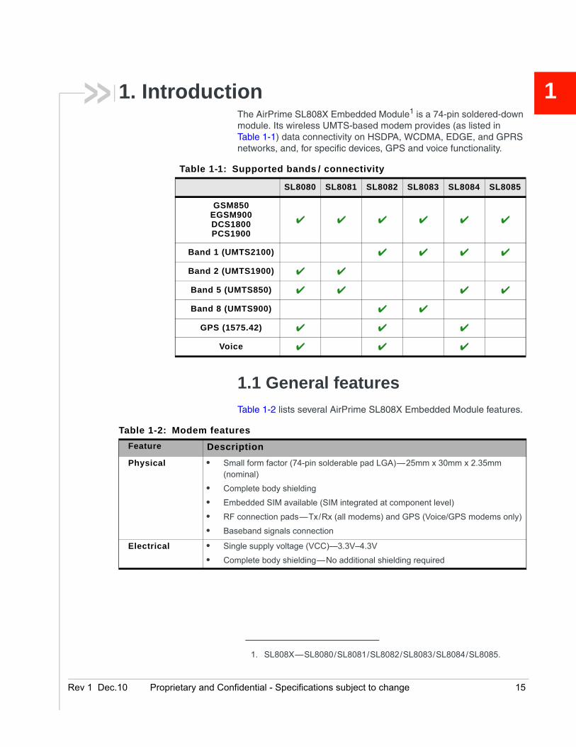
1. IntroductionThe AirPrime SL808X Embedded Module1 is a 74-pin soldered-down module. Its wireless UMTS-based modem provides (as listed in Table 1-1) data connectivity on HSDPA, WCDMA, EDGE, and GPRS networks, and, for specific devices, GPS and voice functionality.1.1 General features
Table 1-2 lists several AirPrime SL808X Embedded Module features.
1. SL808X—SL8080/SL8081/SL8082/SL8083/SL8084/SL8085.
Table 1-1: Supported bands / connectivity
SL8080 SL8081 SL8082 SL8083 SL8084 SL8085
GSM850EGSM900DCS1800PCS1900
Band 1 (UMTS2100)
Band 2 (UMTS1900)
Band 5 (UMTS850)
Band 8 (UMTS900)
GPS (1575.42)
Voice
Table 1-2: Modem features
Feature Description
Physical • Small form factor (74-pin solderable pad LGA)—25mm x 30mm x 2.35mm (nominal)
• Complete body shielding
• Embedded SIM available (SIM integrated at component level)
• RF connection pads—Tx/Rx (all modems) and GPS (Voice/GPS modems only)
• Baseband signals connection
Electrical • Single supply voltage (VCC)—3.3V–4.3V
• Complete body shielding—No additional shielding required
.10 Proprietary and Confidential - Specifications subject to change 15
Product Technical Specification & Customer Design Guidelines
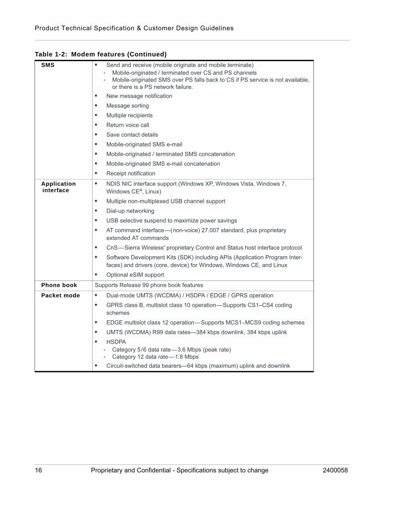
SMS • Send and receive (mobile originate and mobile terminate)· Mobile-originated / terminated over CS and PS channels· Mobile-originated SMS over PS falls back to CS if PS service is not available,
or there is a PS network failure.
• New message notification
• Message sorting
• Multiple recipients
• Return voice call
• Save contact details
• Mobile-originated SMS e-mail
• Mobile-originated / terminated SMS concatenation
• Mobile-originated SMS e-mail concatenation
• Receipt notification
Application interface
• NDIS NIC interface support (Windows XP, Windows Vista, Windows 7, Windows CEa, Linux)
• Multiple non-multiplexed USB channel support
• Dial-up networking
• USB selective suspend to maximize power savings
• AT command interface—(non-voice) 27.007 standard, plus proprietary extended AT commands
• CnS—Sierra Wireless' proprietary Control and Status host interface protocol
• Software Development Kits (SDK) including APIs (Application Program Inter-faces) and drivers (core, device) for Windows, Windows CE, and Linux
• Optional eSIM support
Phone book Supports Release 99 phone book features
Packet mode • Dual-mode UMTS (WCDMA) / HSDPA / EDGE / GPRS operation
• GPRS class B, multislot class 10 operation—Supports CS1–CS4 coding schemes
• EDGE multislot class 12 operation—Supports MCS1–MCS9 coding schemes
• UMTS (WCDMA) R99 data rates—384 kbps downlink, 384 kbps uplink
• HSDPA· Category 5/6 data rate—3.6 Mbps (peak rate)· Category 12 data rate—1.8 Mbps
• Circuit-switched data bearers—64 kbps (maximum) uplink and downlink
Table 1-2: Modem features (Continued)
16 Proprietary and Confidential - Specifications subject to change 2400058

Connectivity /GSM
• Multiple (up to 16) cellular packet data profiles
• Traditional modem COM port support for DUN, CSD, and AT commands (concurrent with NDIS)
• Suspend / Resume
• Sleep mode for minimum idle power draw
• SIM application tool kit with proactive SIM commands
• Enhanced Operator Name String (EONS)
• Profile list. Typical carrier profiles are available in a drop-down list in Watcher; the user can select a profile rather than enter all the parameters.
• Automatic GPRS attach at power-up
• GPRS detach
• GPRS detach only
• Combined GPRS / IMSI detach; MS-initiated and network-initiated detach
• Mobile-originated PDP context activation / deactivation
• Support QoS profile· Release 99 QoS negotiation—Background, Interactive, and Streaming· Release 97—Precedence Class, Reliability Class, Delay Class, Peak
Throughput, Mean Throughput
• Static and Dynamic IP address. The network may assign a fixed IP address or dynamically assign one using DHCP (Dynamic Host Configuration Protocol).
• PAP and CHAP support
• PDP context type (IPv4). IP Packet Data Protocol context
• RFC1144 TCP/IP header compression
• Interaction with existing GSM services (MO/MT SMS voice calls) while:· GPRS is attached, or· In a GPRS data session (class B GPRS suspend / resume procedures)
• Support for EAP-SIM authentication and PC / SC. EAP-SIM is available through:
· The API· AT commands· The PC / SC interface
Voiceb Supports:
• All GSM vocoders, Enhanced Full Rate (EFR), Full Rate (FR), Half Rate (HR), and WCDMA Adaptive Multirate (AMR) encoders
• MO and MT calling
• Echo cancellation and noise reduction
• Emergency calls (112, 110, 911, etc.)
• Incoming call notification
• TTY/TDD compatibility through microphone/speaker connections using the audio interface
Table 1-2: Modem features (Continued)
Rev 1 Dec.10 Proprietary and Confidential - Specifications subject to change 17
Product Technical Specification & Customer Design Guidelines
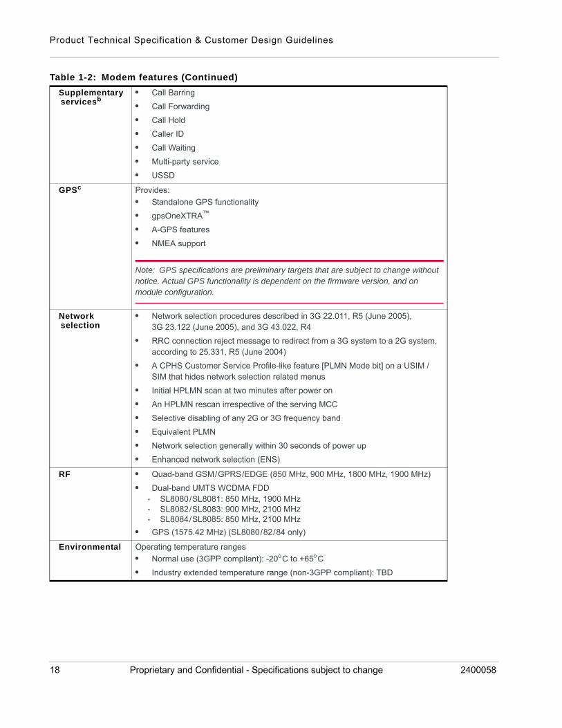
Supplementary servicesb
• Call Barring
• Call Forwarding
• Call Hold
• Caller ID
• Call Waiting
• Multi-party service
• USSD
GPSc Provides:
• Standalone GPS functionality
• gpsOneXTRA™
• A-GPS features
• NMEA support
Note: GPS specifications are preliminary targets that are subject to change without notice. Actual GPS functionality is dependent on the firmware version, and on module configuration.
Network selection
• Network selection procedures described in 3G 22.011, R5 (June 2005), 3G 23.122 (June 2005), and 3G 43.022, R4
• RRC connection reject message to redirect from a 3G system to a 2G system, according to 25.331, R5 (June 2004)
• A CPHS Customer Service Profile-like feature [PLMN Mode bit] on a USIM / SIM that hides network selection related menus
• Initial HPLMN scan at two minutes after power on
• An HPLMN rescan irrespective of the serving MCC
• Selective disabling of any 2G or 3G frequency band
• Equivalent PLMN
• Network selection generally within 30 seconds of power up
• Enhanced network selection (ENS)
RF • Quad-band GSM/GPRS/EDGE (850 MHz, 900 MHz, 1800 MHz, 1900 MHz)
• Dual-band UMTS WCDMA FDD· SL8080/SL8081: 850 MHz, 1900 MHz· SL8082/SL8083: 900 MHz, 2100 MHz· SL8084/SL8085: 850 MHz, 2100 MHz
• GPS (1575.42 MHz) (SL8080/82/84 only)
Environmental Operating temperature ranges
• Normal use (3GPP compliant): -20C to +65C• Industry extended temperature range (non-3GPP compliant): TBD
Table 1-2: Modem features (Continued)
18 Proprietary and Confidential - Specifications subject to change 2400058
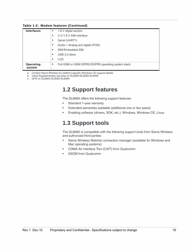
1.2 Support features
The SL808X offers the following support features:
• Standard 1-year warranty
• Extended warranties available (additional one or two years)
• Enabling software (drivers, SDK, etc.): Windows, Windows CE, Linux
1.3 Support tools
The SL808X is compatible with the following support tools from Sierra Wireless and authorized third parties:
• Sierra Wireless Watcher connection manager (available for Windows and Mac operating systems)
• CDMA Air Interface Tool (CAIT) from Qualcomm
• QXDM from Qualcomm
Interfaces • 1.8 V digital section
• 3 V/1.8 V SIM interface
• Serial (UART1)
• Audio—Analog and digital (PCM)
• SIM/Embedded SIM
• USB 2.0 slave
• LCD
Operating system
• Full GSM or GSM/GPRS/EGPRS operating system stack
a. Contact Sierra Wireless for platform-specific Windows CE support details.b. Voice/Supplementary services on SL8080/SL8082/SL8084c. GPS on SL8080/SL8082/SL8084
Table 1-2: Modem features (Continued)
Rev 1 Dec.10 Proprietary and Confidential - Specifications subject to change 19

Product Technical Specification & Customer Design Guidelines
1.4 Accessories
The Universal SL Dev Kit includes:
• Embedded Modem Interface Kit
• Documentation suite
• Initial allotment of support hours
• USB cable
• Serial cable
• Power supply
• Quad-band antenna
• Handset
1.5 Hardware development components
Sierra Wireless manufactures two hardware development components to facilitate the hardware integration process:
• AirPrime SL Socket-Up Board—Adapter board into which an SL module is embedded. This board may be used as a stand-alone platform for basic hardware development. See Reference schematic on page 40 for details.
• AirPrime SL Development Kit—Hardware development platform that integrates with the socket-up board. The development kit provides access to all of the interfaces supported by the SL module.
For instructions on using the SL Development Kit, see [1] SL Dev Kit Quick Start Guide (TBD).
1.6 Ordering information
To order, contact the Sierra Wireless Sales Desk at +1 (604) 232-1488 between 8 AM and 5 PM Pacific Time.
1.7 Environmental issues
1.7.1 RoHS directive compliant
The AirPrime SL808X Embedded Module is compliant with RoHS Directive 2002/95/EC which sets limits for the use of certain restricted hazardous substances. This directive states that "from 1st July 2006, new electrical and electronic equipment put on the market does not contain lead, mercury, cadmium, hexavalent chromium, polybrominated biphenyls (PBB) or polybrominated diphenyl ethers (PBDE)".
20 Proprietary and Confidential - Specifications subject to change 2400058
1.7.2 Disposing of the product
This electronic product is subject to the EU Directive 2002/96/EC for Waste Electrical and Electronic Equipment (WEEE). As such, this product must not be disposed off at a municipal waste collection point. Please refer to local regulations for directions on how to dispose of this product in an environmental friendly manner.
Rev 1 Dec.10 Proprietary and Confidential - Specifications subject to change 21
Product Technical Specification & Customer Design Guidelines
22 Proprietary and Confidential - Specifications subject to change 2400058

Rev 1 Dec
2
2: Functional Specifications2.1 Functional architecture
The global architecture of the AirPrime SL808X Embedded Module is described in Figure 2-1.
Figure 2-1: Functional architecture
2.1.1 Chipsets
SL808X modems are based on Qualcomm single chip solutions (integrated baseband processor, RF transceiver, and power management IC):
• Voice modems: SL8080/82/84—QSC6270
• Data modems: SL8081/83/85—MDM6270
2.2 Extended AT commands
Several proprietary AT commands are available for AirPrime embedded modules to use in hardware integration design and testing (these commands are NOT intended for use by end users). For lists
AirP
rime
SL8
08X
Sca
labl
e LG
A p
adSupply Interface
Power RF Interface
Audio EXT_IT
SPI1
PCM
I2C
UART1 GPIO
USB ADC
SIM 1.8V/3V
XTAL EBI
Audio Filter
USB detection
MemoryFLASH / SRAM
RF Transceiver
RF Front End
Antenna
.10 Proprietary and Confidential - Specifications subject to change 23
Product Technical Specification & Customer Design Guidelines
of all available commands and descriptions of their functionality, refer to [3] AirPrime MC8xxx Embedded Modules Extended AT Command Reference and [2] AirCard/AirPrime UMTS Devices Supported AT Command Reference.
24 Proprietary and Confidential - Specifications subject to change 2400058
Rev 1 Dec
3
Signal /Name
VCC_3V6
VREF_1V
GND
a. Hoswith
3: Technical Specifications
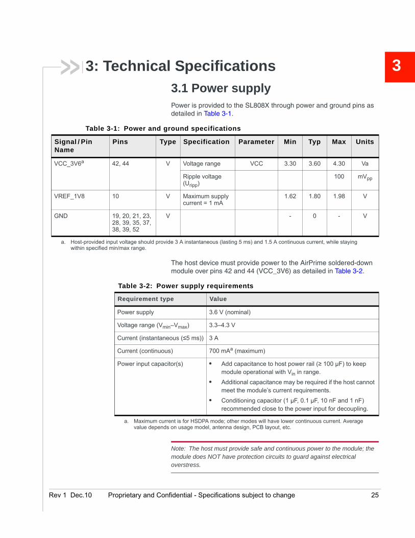
3.1 Power supplyPower is provided to the SL808X through power and ground pins as detailed in Table 3-1.
The host device must provide power to the AirPrime soldered-down module over pins 42 and 44 (VCC_3V6) as detailed in Table 3-2.
Note: The host must provide safe and continuous power to the module; the module does NOT have protection circuits to guard against electrical overstress.
Table 3-1: Power and ground specifications
Pin Pins Type Specification Parameter Min Typ Max Units
a 42, 44 V Voltage range VCC 3.30 3.60 4.30 Va
Ripple voltage (Uripp)
100 mVpp
8 10 V Maximum supply current = 1 mA
1.62 1.80 1.98 V
19, 20, 21, 23, 28, 39, 35, 37, 38, 39, 52
V - 0 - V
t-provided input voltage should provide 3 A instantaneous (lasting 5 ms) and 1.5 A continuous current, while staying in specified min/max range.
Table 3-2: Power supply requirements
Requirement type Value
Power supply 3.6 V (nominal)
Voltage range (Vmin–Vmax) 3.3–4.3 V
Current (instantaneous (≤5 ms)) 3 A
Current (continuous) 700 mAa (maximum)
Power input capacitor(s) • Add capacitance to host power rail (≥ 100 µF) to keep module operational with Vin in range.
• Additional capacitance may be required if the host cannot meet the module’s current requirements.
• Conditioning capacitor (1 µF, 0.1 µF, 10 nF and 1 nF) recommended close to the power input for decoupling.
a. Maximum current is for HSDPA mode; other modes will have lower continuous current. Average value depends on usage model, antenna design, PCB layout, etc.
.10 Proprietary and Confidential - Specifications subject to change 25
Product Technical Specification & Customer Design Guidelines
3.1.1 Burst transmission current requirements
The power supply must be able to deliver high current peaks in a short time due to the burst transmission nature of GSM. During these peaks, the ripple (Uripp) on the supply voltage must not exceed the level noted in Table 3-1 on page 25.
Table 3-3 describes radio burst rates in connected mode. For detailed power consumption figures, see Table 6-2 on page 77.
3.1.2 Power input (VCC_3V6)
An external power supply uses the VCC_3V6 pins to:
• Supply the AirPrime SL808X Embedded Module.
• Directly supply the RF components with 3.6 V.· It is essential to keep a minimum voltage ripple at this connection in order
to avoid any phase error or spectrum modulation degradation.· Insufficient power supply can significantly affect RF performance (TX
power, modulation spectrum, EMC performance, spurious emission, frequency error, etc.).
• Provide reference voltage VREF_1V8 (through several internal regulators) for the baseband signals. The host should draw less than 1 mA on this rail.
When the AirPrime SL808X Embedded Module is supplied with a battery, the total impedance (battery + protections + PCB) should be such that the supply will be >= 3.3 V during GSM burst mode operation (drawing a maximum peak current of 2.2 A for 577 µs (one slot) or 1154 µs (two slots) TX.
3.1.3 Start-up current
During the first second following Power ON, a current peak occurs. This current peak (tStartup) has a duration of about 165 ms (typical).
Table 3-4 indicates the expected peak current range.
Table 3-3: Radio burst rates — Connected mode
GSM / GPRS
Multislot classa
a. (TBD) Table contents to be updated to classes supported by SL808X.
RF Power Amplifier current
Burst duration PeriodRising time
Class 102.0 A peak
577 µs 4.615 ms10 µs
Class 12 1154 µs 4.615 ms
Table 3-4: Start-up current peak range
Current peak at ambient
temperature (25°C)
VCC_3V6min
(3.3 V)
VCC_3V6typ
(3.6 V)
VCC_3V6max
(4.3 V)
tStartup 150 mA 140 mA 115 mA
26 Proprietary and Confidential - Specifications subject to change 2400058

3.2 Ground connection
The AirPrime SL808X Embedded Module shielding case is the grounding. The ground must be connected on the motherboard through a complete layer on the PCB.
The ground connection is made by soldering the LGA ground pins and rectangular ground pad to the ground plane of the application board. For more information about ground connection, see Ground plane and shielding connection on page 97.
3.3 Decoupling of power supply signals
Although the AirPrime SL808X Embedded Module has embedded decoupling capacitors on the VCC_3V6 lines, additional decoupling may be required:
• EMI/RFI issues—Parallel 33 pF capacitors close to the embedded module.
• TDMA noise (217 Hz)—Low frequency decoupling capacitors (22–100 µF) can be used to reduce noise.
3.4 Mechanical specifications
This section describes mechanical specifications for the AirPrime SL808X Embedded Module. For additional mechanical and environmental specifications, refer to [5] Sierra Wireless Reliability Specification.
Table 3-5: Mechanical specifications
Specification Details
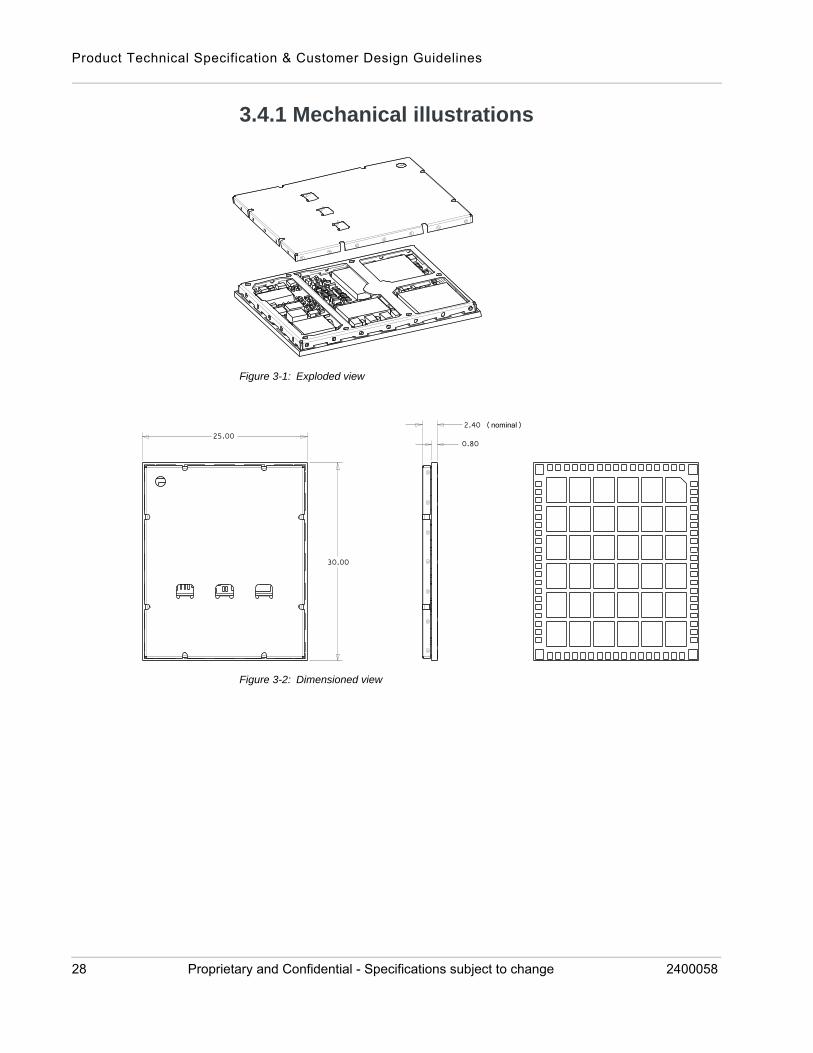
Form factor The SL808X is a 74-pin LGA soldered-down module with a two-piece shielded case.
Dimensions (nominal)
Length: 30 mm Width: 25 mmThickness: 2.40 mm (nominal)/2.55 mm (maximum)Weight: approximately 3.5 g
Rev 1 Dec.10 Proprietary and Confidential - Specifications subject to change 27
Product Technical Specification & Customer Design Guidelines
3.4.1 Mechanical illustrations
Figure 3-1: Exploded view
Figure 3-2: Dimensioned view
2.4 (nominal)
0.8025.00
30.00
28 Proprietary and Confidential - Specifications subject to change 2400058

3.5 Labeling
Figure 3-3: Unit label
The SL808X label is non-removable and contains:
• Sierra Wireless logo and product name. (Figure 3-3 uses ‘X’ to represent the actual product name. For example, SL8080, SL8081, SL8082, etc.)
• Factory Serial Number (FSN) and IMEI number are shown in alphanumeric and Data Matrix (ECC200) 2D barcode formats
• SKU number (when required)
• Manufacturing date code (incorporated into FSN)
• Licensed vendor logo when required
• Device-specific regulatory certification marks (for example, FCC/IC, CE, A-Tick)
Note: The SL808X supports OEM partner specific label requirements.
3.6 Embedded SIM (eSIM)
The AirPrime SL808X Embedded Module is available with an embedded SIM solution that eliminates design issues related to working with a consumer-style SIM card, including:
• Improved environmental performance—The embedded SIM operates in extreme temperatures, and has higher vibration and humidity tolerances.
• Minimized size—The embedded SIM eliminates the requirements of a SIM card holder and plastic SIM, and the module is the same size with or without the embedded SIM.
• Service provider choice—You can provision the SIM with your preferred service provider or carrier, or take advantage of Sierra Wireless’ existing carrier partnerships.
• Subscription portability and security—An integrated switch allows devel-opers to provide the flexibility of switching between the embedded SIM and an external SIM as required.
Rev 1 Dec.10 Proprietary and Confidential - Specifications subject to change 29
Product Technical Specification & Customer Design Guidelines
• Simplified logistics—The embedded SIM does not need to be tracked, stored, or activated (as would a physical SIM card).
3.7 Thermal considerations
When transmitting, the AirPrime SL808X Embedded Module can generate significant amounts of heat (due to the internal Power Amplifier) that must be dissipated in the host device for safety and performance reasons.
The amount of thermal dissipation required depends on the following factors:
• Supply voltage—Maximum power dissipation for these modules can be up to 2.0 W at voltage supply limits.
• Usage—Typical power dissipation values depend on the location within the host, amount of data transferred, etc.
You can enhance heat dissipation by:
• Maximizing airflow over/around the module
• Locating the module away from other hot components
You can use !PCTEMP or !GSTATUS to return the module’s current temperature. See [2] AirCard/AirPrime UMTS Devices Supported AT Command Reference for details.
3.8 SED (Smart Error Detection)
The AirPrime SL808X Embedded Module modules use a form of SED to track premature modem resets. In such cases, the module automatically forces a pause in boot-and-hold mode at power-on to accept an expected firmware download to resolve the problem.
1. Module tracks consecutive resets within 30 seconds of power-on.
2. After a third consecutive reset, the module waits in boot-and-hold mode for a firmware download to resolve the power-cycle problem.
3.9 Firmware upgrade
Firmware upgrades are downloaded to the modem over the USB or UART interfaces. Contact your Sierra Wireless account representative for assistance.
30 Proprietary and Confidential - Specifications subject to change 2400058
Rev 1 Dec
4
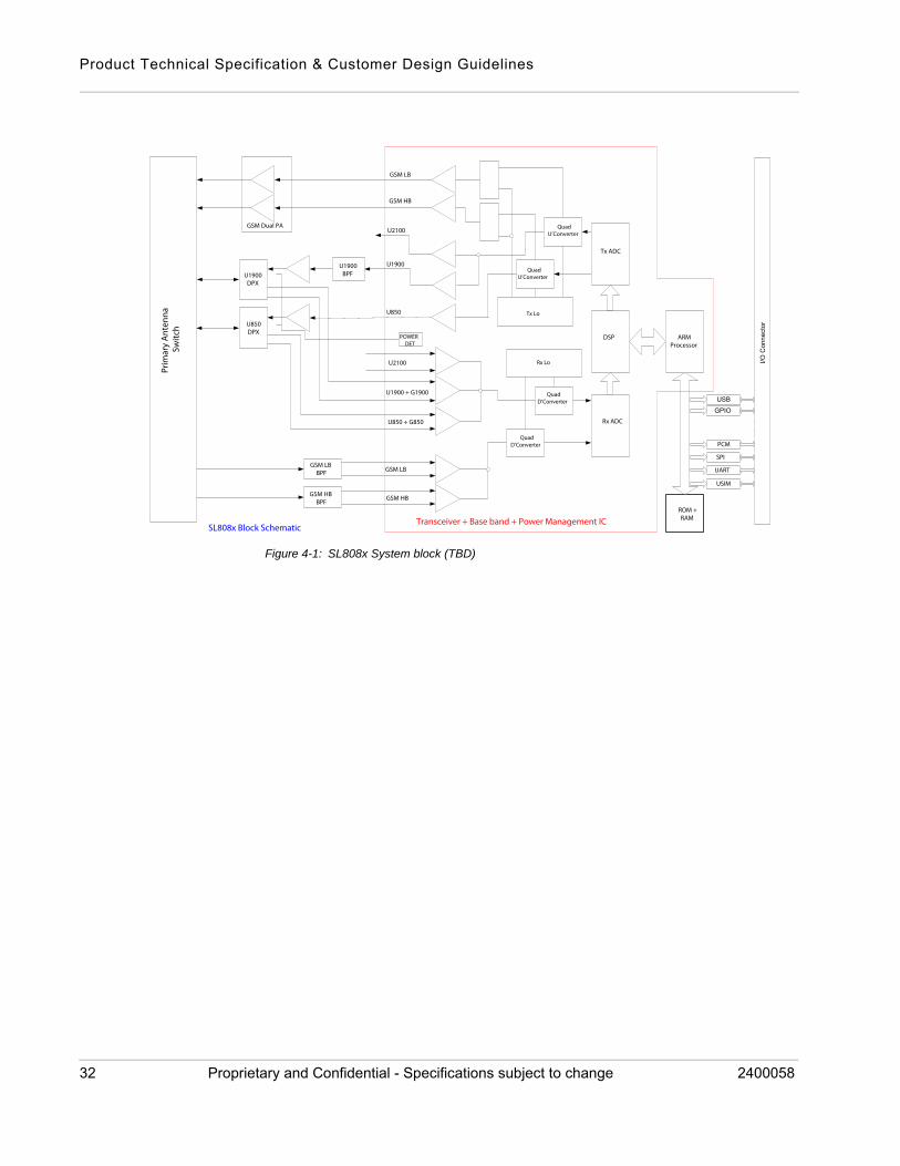
4: Interfaces4.1 System design
This chapter describes the AirPrime SL808X Embedded Module’s LGA pad configuration (see Pin configuration on page 33) and supported interfaces (Table 4-1).
The SL808X has two main interface areas—the host I/O perimeter I/O ports (pins) and the RF ports. Figure 4-1 portrays the AirPrime SL808X Embedded Module’s system block with these interface areas identified.
Table 4-1: Available interfaces and signals
NameDriven by AT commands
General purpose input/output on page 40
Main serial link (UART1) on page 41
SIM interface on page 42
USB 2.0 interface on page 44
RF interface on page 47
Analog audio interface on page 52
Digital audio interface (PCM) on page 62
JTAG interface on page 64
.10 Proprietary and Confidential - Specifications subject to change 31
Product Technical Specification & Customer Design Guidelines
Figure 4-1: SL808x System block (TBD)
Prim
ary
An
ten
na
Swit
ch
U850 + G850
U1900 + G1900
U850
U1900U1900BPF
POWERDET
Tx Lo
QuadU’Converter
QuadU’Converter
Rx Lo
QuadD’Converter
QuadD’Converter
GSM LB
GSM HB
GSM LB
GSM HB
U2100
U2100
Transceiver + Base band + Power Management ICSL808x Block Schematic
U850DPX
U1900DPX
GSM Dual PA
Rx ADC
Tx ADC
DSP ARMProcessor
ROM +RAM
USB
GPIO
I/O C
onne
ctor
GSM LBBPF
GSM HBBPF
UART
USIM
PCM
SPI
32 Proprietary and Confidential - Specifications subject to change 2400058
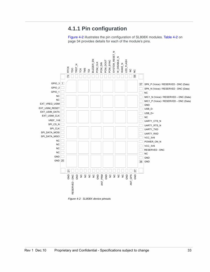
4.1.1 Pin configuration
Figure 4-2 illustrates the pin configuration of SL808X modules. Table 4-2 on page 34 provides details for each of the module’s pins.
Figure 4-2: SL808X device pinouts
GPIO_3
GPIO_2
GPIO_1
NC
NC
EXT_VREG_USIM
EXT_USIM_RESET
EXT_USIM_DATA
EXT_USIM_CLK
NC
SPI_CS_N
SPI_CLK
SPI_DATA_MOSI
SPI_DATA_MISO
NC
NC
NC
NC
GND
GND
POWER_ON_N
VCC_3V6
SPK_P (Voice) / RESERVED - DNC (Data)
SPK_N (Voice) / RESERVED - DNC (Data)
NC
MIC1_N (Voice) / RESERVED – DNC (Data)
MIC1_P (Voice) / RESERVED – DNC (Data)
GND
USB_D-
USB_D+
NC
UART1_CTS_N
UART1_RTS_N
UART1_TXD
UART1_RXD
VCC_3V6
RESERVED - DNC
NC
GND
GND
1
20
21
37
38
57
5874
NC
VREF_1V8
LED
_FLA
SH
WA
KE
_N
W_D
ISA
BL
E_
N
SY
ST
EM
_R
ES
ET
_N
PC
M_S
YN
C
PC
M_
DO
UT
PC
M_D
IN
PC
M_C
LK
BU
ZZ
ER
_EN
TD
I
TM
S
TC
K
TR
ST
_N
TD
O
GN
D
AN
T_G
PS
GN
D
NC
NC
NC
NC
GN
D
AN
T_P
RM
GN
D
NC
NC
NC
NC
GN
D
GN
DR
TC
K
RE
SE
RV
ED
- D
NC
Rev 1 Dec.10 Proprietary and Confidential - Specifications subject to change 33
Product Technical Specification & Customer Design Guidelines
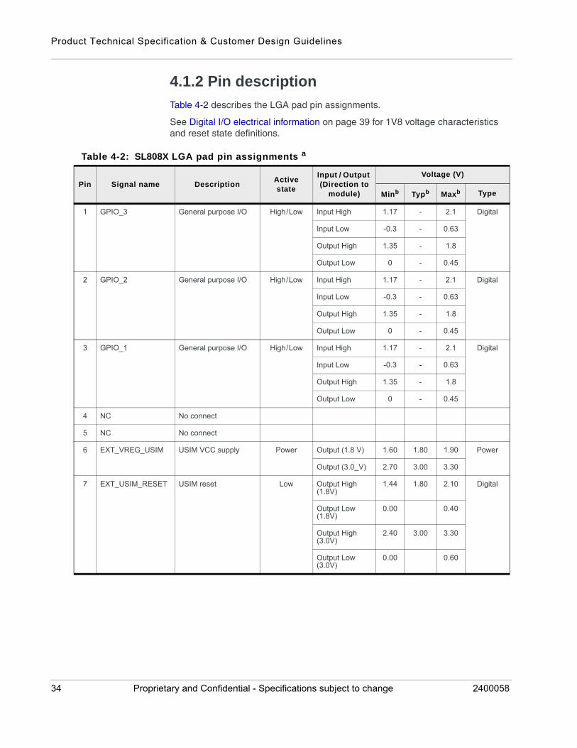
4.1.2 Pin description
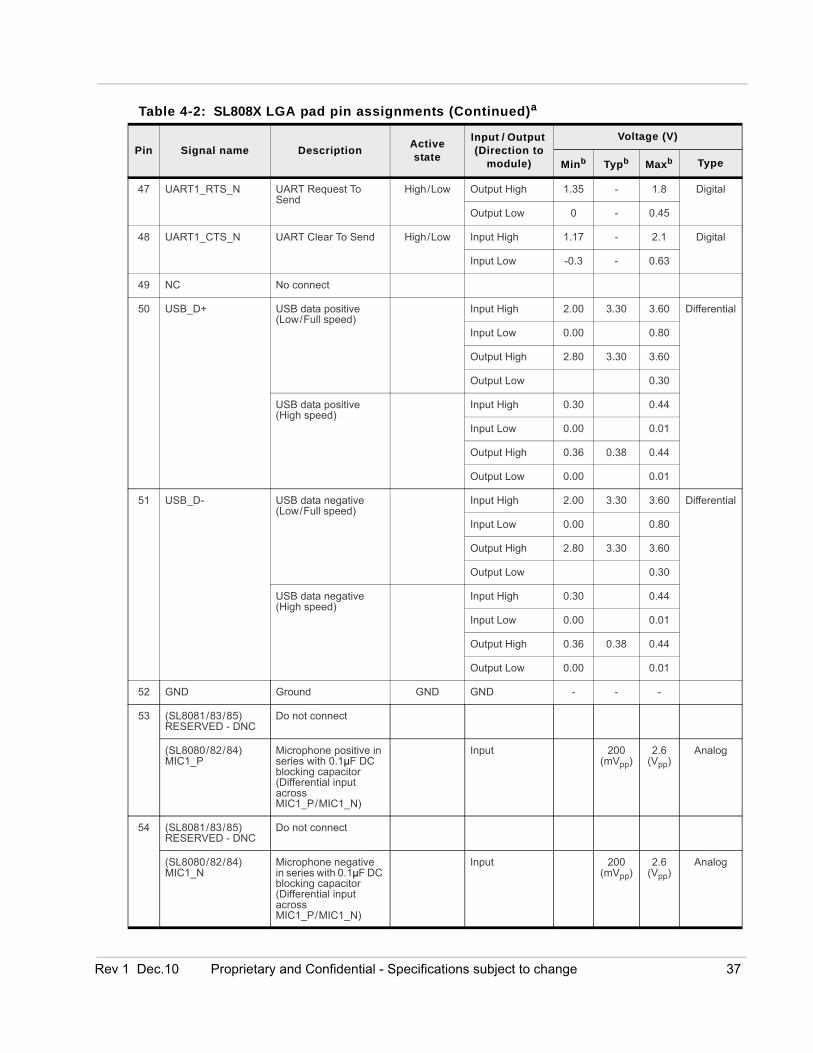
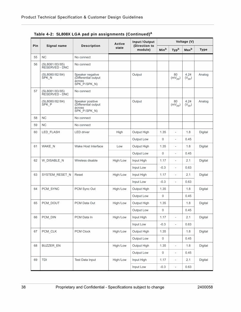
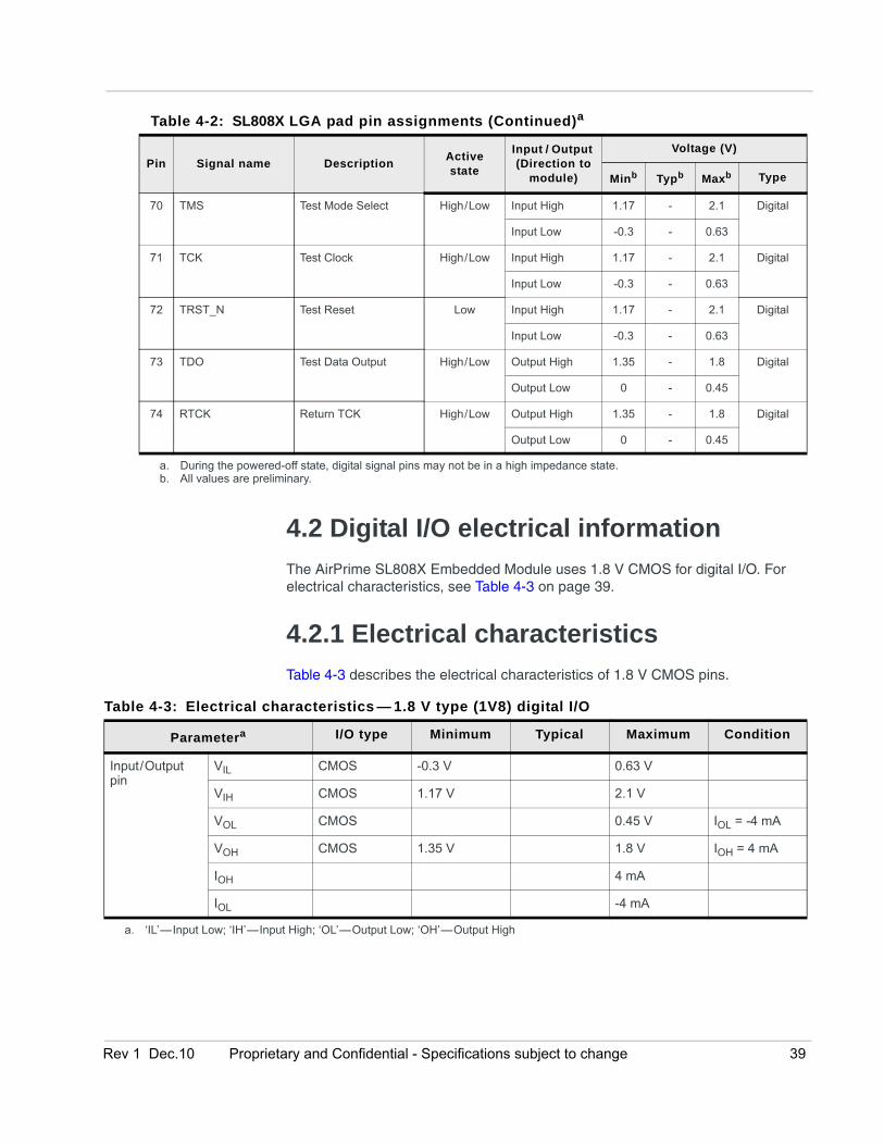
Table 4-2 describes the LGA pad pin assignments.
See Digital I/O electrical information on page 39 for 1V8 voltage characteristics and reset state definitions.
Table 4-2: SL808X LGA pad pin assignments a
Pin Signal name DescriptionActive state
Input / Output (Direction to
module)
Voltage (V)
Minb Typb Maxb Type
1 GPIO_3 General purpose I/O High/Low Input High 1.17 - 2.1 Digital
Input Low -0.3 - 0.63
Output High 1.35 - 1.8
Output Low 0 - 0.45
2 GPIO_2 General purpose I/O High/Low Input High 1.17 - 2.1 Digital
Input Low -0.3 - 0.63
Output High 1.35 - 1.8
Output Low 0 - 0.45
3 GPIO_1 General purpose I/O High/Low Input High 1.17 - 2.1 Digital
Input Low -0.3 - 0.63
Output High 1.35 - 1.8
Output Low 0 - 0.45
4 NC No connect
5 NC No connect
6 EXT_VREG_USIM USIM VCC supply Power Output (1.8 V) 1.60 1.80 1.90 Power
Output (3.0_V) 2.70 3.00 3.30
7 EXT_USIM_RESET USIM reset Low Output High (1.8V)
1.44 1.80 2.10 Digital
Output Low (1.8V)
0.00 0.40
Output High (3.0V)
2.40 3.00 3.30
Output Low (3.0V)
0.00 0.60
34 Proprietary and Confidential - Specifications subject to change 2400058
8 EXT_USIM_DATA USIM I/O pin Input High (1.8 V)
1.26 2.10 Digital
Input Low (1.8 V)
0.00 0.40
Output High (1.8 V)
1.26 1.80 2.10
Output Low (1.8 V)
0.00 0.40
Input High (3.0 V)
2.10 3.30
Input Low (3.0 V)
0.00 0.60
Output High (3.0 V)
2.10 3.00 3.30
Output Low (3.0 V)
0.00 0.60
9 EXT_USIM_CLK USIM clock Output High (1.8V)
1.26 1.80 2.10 Digital
Output Low (1.8V)
0.00 0.40
Output High (3.0V)
2.10 3.00 3.30
Output Low (3.0V)
0.00 0.60
10 VREF_1V8 1.8 V LDO High(when
module is on)
Output 1.62 1.8 1.98 Power
11 SPI_CS_N SPI chip select Low Output High 1.35 - 1.8 Digital
Output Low 0 - 0.45
12 SPI_CLK SPI clock Output High 1.35 - 1.8 Digital
Output Low 0 - 0.45
13 SPI_DATA_MOSI SPI Master Output / Slave Input data pin
Output High 1.35 - 1.8 Digital
Output Low 0 - 0.45
14 SPI_DATA_MISO SPI Master Input / Slave Output data pin
Input High 1.17 - 2.1 Digital
Input Low -0.3 - 0.63
15 NC No connect
16 NC No connect
17 NC No connect
18 NC No connect
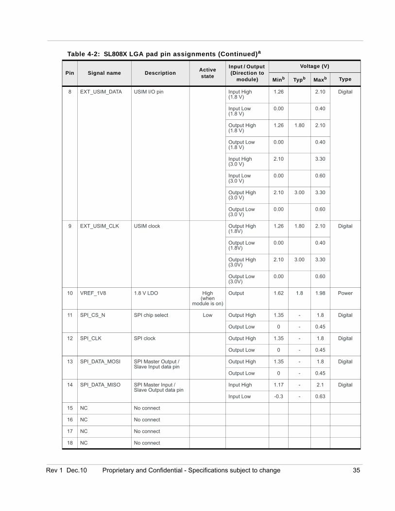
Table 4-2: SL808X LGA pad pin assignments (Continued)a
Pin Signal name DescriptionActive state
Input / Output (Direction to
module)
Voltage (V)
Minb Typb Maxb Type
Rev 1 Dec.10 Proprietary and Confidential - Specifications subject to change 35
Product Technical Specification & Customer Design Guidelines
19 GND Ground GND GND - - -
20 GND Ground GND GND - - -
21 GND Ground GND GND - - -
22 RESERVED - DNC No connect
23 GND Ground GND GND - - -
24 NC No connect
25 NC No connect
26 NC No connect
27 NC No connect
28 GND Ground GND GND - - -
29 ANT_PRM Main (primary) antenna
Input/Output Refer to RF specifications
RF
30 GND Ground GND GND - - -
31 NC No connect
32 NC No connect
33 NC No connect
34 NC No connect
35 GND Ground GND GND - - -
36 ANT_GPS GPS antenna Input Refer to RF specifications
RF
37 GND Ground GND GND - - -
38 GND Ground GND GND - - -
39 GND Ground GND GND - - -
40 NC No connect
41 RESERVED - DNC No connect
42 VCC_3V6 3.6 V supply Power Input 3.30 3.60 4.30 Power
43 POWER_ON_N Power on Input 0 2.6 Digital
44 VCC_3V6 3.6 V supply Power Input 3.30 3.60 4.30 Power
45 UART1_RXD UART Receive Data High/Low Input High 1.17 - 2.1 Digital
Input Low -0.3 - 0.63
46 UART1_TXD UART Transmit Data High/Low Output High 1.35 - 1.8 Digital
Output Low 0 - 0.45
Table 4-2: SL808X LGA pad pin assignments (Continued)a
Pin Signal name DescriptionActive state
Input / Output (Direction to
module)
Voltage (V)
Minb Typb Maxb Type
36 Proprietary and Confidential - Specifications subject to change 2400058
47 UART1_RTS_N UART Request To Send
High/Low Output High 1.35 - 1.8 Digital
Output Low 0 - 0.45
48 UART1_CTS_N UART Clear To Send High/Low Input High 1.17 - 2.1 Digital
Input Low -0.3 - 0.63
49 NC No connect
50 USB_D+ USB data positive(Low/Full speed)
Input High 2.00 3.30 3.60 Differential
Input Low 0.00 0.80
Output High 2.80 3.30 3.60
Output Low 0.30
USB data positive(High speed)
Input High 0.30 0.44
Input Low 0.00 0.01
Output High 0.36 0.38 0.44
Output Low 0.00 0.01
51 USB_D- USB data negative(Low/Full speed)
Input High 2.00 3.30 3.60 Differential
Input Low 0.00 0.80
Output High 2.80 3.30 3.60
Output Low 0.30
USB data negative(High speed)
Input High 0.30 0.44
Input Low 0.00 0.01
Output High 0.36 0.38 0.44
Output Low 0.00 0.01
52 GND Ground GND GND - - -
53 (SL8081/83/85)RESERVED - DNC
Do not connect
(SL8080/82/84)MIC1_P
Microphone positive in series with 0.1µF DC blocking capacitor (Differential input across MIC1_P/MIC1_N)
Input 200 (mVpp)
2.6 (Vpp)
Analog
54 (SL8081/83/85)RESERVED - DNC
Do not connect
(SL8080/82/84)MIC1_N
Microphone negative in series with 0.1µF DC blocking capacitor (Differential input across MIC1_P/MIC1_N)
Input 200 (mVpp)
2.6 (Vpp)
Analog
Table 4-2: SL808X LGA pad pin assignments (Continued)a
Pin Signal name DescriptionActive state
Input / Output (Direction to
module)
Voltage (V)
Minb Typb Maxb Type
Rev 1 Dec.10 Proprietary and Confidential - Specifications subject to change 37
Product Technical Specification & Customer Design Guidelines
55 NC No connect
56 (SL8081/83/85)RESERVED - DNC
No connect
(SL8080/82/84)SPK_N
Speaker negative (Differential output across SPK_P/SPK_N)
Output 80 (mVpp)
4.24 (Vpp)
Analog
57 (SL8081/83/85)RESERVED - DNC
No connect
(SL8080/82/84)SPK_P
Speaker positive (Differential output across SPK_P/SPK_N)
Output 80 (mVpp)
4.24 (Vpp)
Analog
58 NC No connect
59 NC No connect
60 LED_FLASH LED driver High Output High 1.35 - 1.8 Digital
Output Low 0 - 0.45
61 WAKE_N Wake Host Interface Low Output High 1.35 - 1.8 Digital
Output Low 0 - 0.45
62 W_DISABLE_N Wireless disable High/Low Input High 1.17 - 2.1 Digital
Input Low -0.3 - 0.63
63 SYSTEM_RESET_N Reset High/Low Input High 1.17 - 2.1 Digital
Input Low -0.3 - 0.63
64 PCM_SYNC PCM Sync Out High/Low Output High 1.35 1.8 Digital
Output Low 0 0.45
65 PCM_DOUT PCM Data Out High/Low Output High 1.35 1.8 Digital
Output Low 0 0.45
66 PCM_DIN PCM Data In High/Low Input High 1.17 - 2.1 Digital
Input Low -0.3 - 0.63
67 PCM_CLK PCM Clock High/Low Output High 1.35 1.8 Digital
Output Low 0 0.45
68 BUZZER_EN High/Low Output High 1.35 - 1.8 Digital
Output Low 0 - 0.45
69 TDI Test Data Input High/Low Input High 1.17 - 2.1 Digital
Input Low -0.3 - 0.63
Table 4-2: SL808X LGA pad pin assignments (Continued)a
Pin Signal name DescriptionActive state
Input / Output (Direction to
module)
Voltage (V)
Minb Typb Maxb Type
38 Proprietary and Confidential - Specifications subject to change 2400058
4.2 Digital I/O electrical information
The AirPrime SL808X Embedded Module uses 1.8 V CMOS for digital I/O. For electrical characteristics, see Table 4-3 on page 39.
4.2.1 Electrical characteristics
Table 4-3 describes the electrical characteristics of 1.8 V CMOS pins.
70 TMS Test Mode Select High/Low Input High 1.17 - 2.1 Digital
Input Low -0.3 - 0.63
71 TCK Test Clock High/Low Input High 1.17 - 2.1 Digital
Input Low -0.3 - 0.63
72 TRST_N Test Reset Low Input High 1.17 - 2.1 Digital
Input Low -0.3 - 0.63
73 TDO Test Data Output High/Low Output High 1.35 - 1.8 Digital
Output Low 0 - 0.45
74 RTCK Return TCK High/Low Output High 1.35 - 1.8 Digital
Output Low 0 - 0.45
a. During the powered-off state, digital signal pins may not be in a high impedance state.b. All values are preliminary.
Table 4-2: SL808X LGA pad pin assignments (Continued)a
Pin Signal name DescriptionActive state
Input / Output (Direction to
module)
Voltage (V)
Minb Typb Maxb Type
Table 4-3: Electrical characteristics — 1.8 V type (1V8) digital I/O
Parametera I/O type Minimum Typical Maximum Condition
Input/Output pin
VIL CMOS -0.3 V 0.63 V
VIH CMOS 1.17 V 2.1 V
VOL CMOS 0.45 V IOL = -4 mA
VOH CMOS 1.35 V 1.8 V IOH = 4 mA
IOH 4 mA
IOL -4 mA
a. ‘IL’—Input Low; ‘IH’—Input High; ‘OL’—Output Low; ‘OH’—Output High
Rev 1 Dec.10 Proprietary and Confidential - Specifications subject to change 39
Product Technical Specification & Customer Design Guidelines
4.2.2 Signal reset states
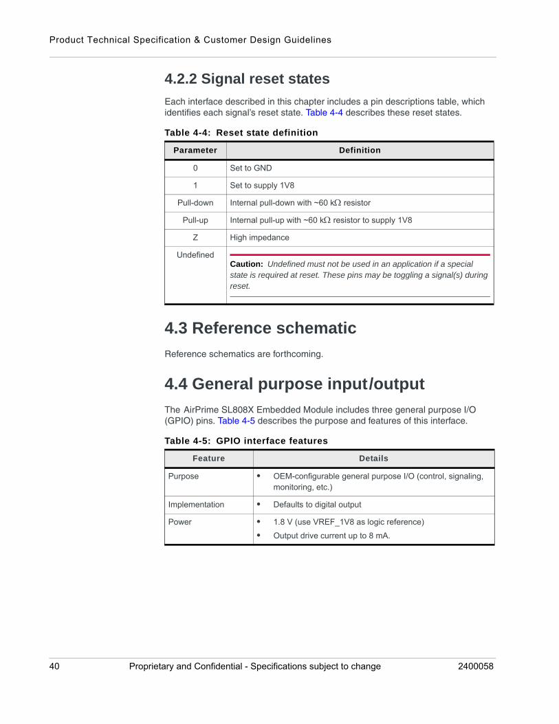
Each interface described in this chapter includes a pin descriptions table, which identifies each signal’s reset state. Table 4-4 describes these reset states.
4.3 Reference schematic
Reference schematics are forthcoming.
4.4 General purpose input/output
The AirPrime SL808X Embedded Module includes three general purpose I/O (GPIO) pins. Table 4-5 describes the purpose and features of this interface.
Table 4-4: Reset state definition
Parameter Definition
0 Set to GND
1 Set to supply 1V8
Pull-down Internal pull-down with ~60 k resistor
Pull-up Internal pull-up with ~60 k resistor to supply 1V8
Z High impedance
UndefinedCaution: Undefined must not be used in an application if a special state is required at reset. These pins may be toggling a signal(s) during reset.
Table 4-5: GPIO interface features
Feature Details
Purpose • OEM-configurable general purpose I/O (control, signaling, monitoring, etc.)
Implementation • Defaults to digital output
Power • 1.8 V (use VREF_1V8 as logic reference)
• Output drive current up to 8 mA.
40 Proprietary and Confidential - Specifications subject to change 2400058
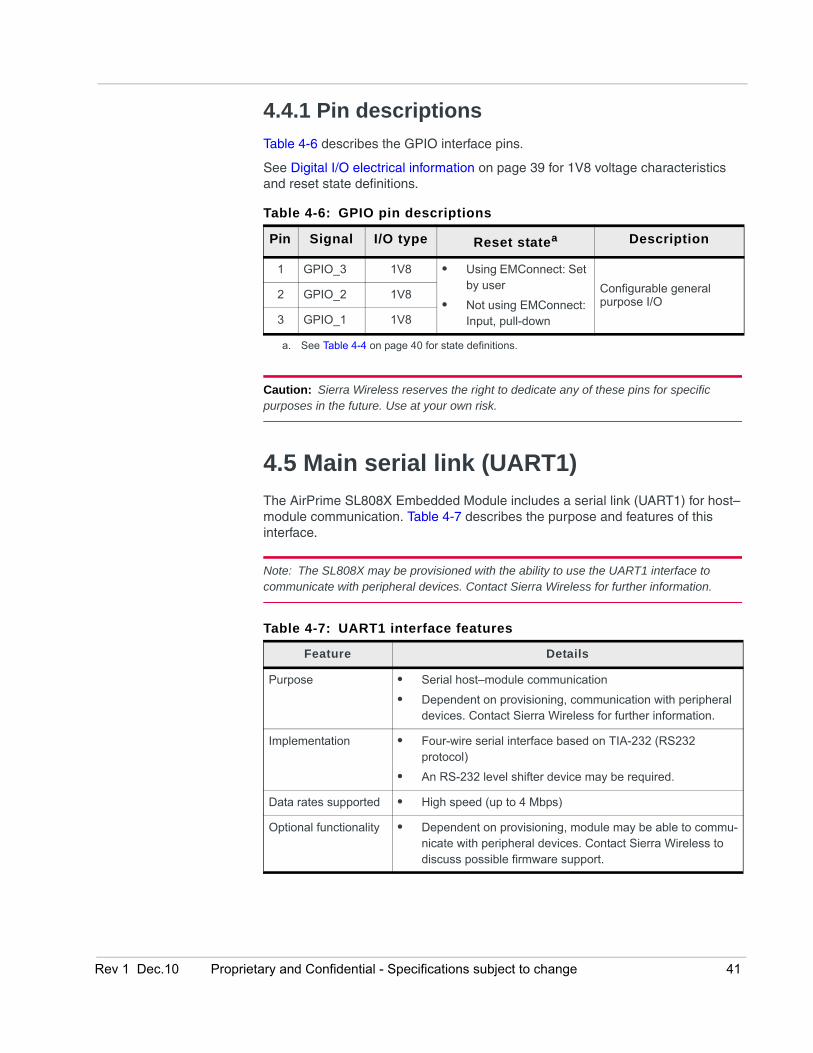
4.4.1 Pin descriptions
Table 4-6 describes the GPIO interface pins.
See Digital I/O electrical information on page 39 for 1V8 voltage characteristics and reset state definitions.
Caution: Sierra Wireless reserves the right to dedicate any of these pins for specific purposes in the future. Use at your own risk.
4.5 Main serial link (UART1)
The AirPrime SL808X Embedded Module includes a serial link (UART1) for host–module communication. Table 4-7 describes the purpose and features of this interface.
Note: The SL808X may be provisioned with the ability to use the UART1 interface to communicate with peripheral devices. Contact Sierra Wireless for further information.
Table 4-6: GPIO pin descriptions
Pin Signal I/O type Reset statea
a. See Table 4-4 on page 40 for state definitions.
Description
1 GPIO_3 1V8 • Using EMConnect: Set by user
• Not using EMConnect: Input, pull-down
Configurable general purpose I/O
2 GPIO_2 1V8
3 GPIO_1 1V8
Table 4-7: UART1 interface features
Feature Details
Purpose • Serial host–module communication
• Dependent on provisioning, communication with peripheral devices. Contact Sierra Wireless for further information.
Implementation • Four-wire serial interface based on TIA-232 (RS232 protocol)
• An RS-232 level shifter device may be required.
Data rates supported • High speed (up to 4 Mbps)
Optional functionality • Dependent on provisioning, module may be able to commu-nicate with peripheral devices. Contact Sierra Wireless to discuss possible firmware support.
Rev 1 Dec.10 Proprietary and Confidential - Specifications subject to change 41
Product Technical Specification & Customer Design Guidelines
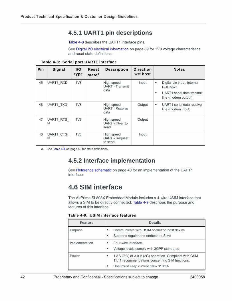
4.5.1 UART1 pin descriptions
Table 4-8 describes the UART1 interface pins.
See Digital I/O electrical information on page 39 for 1V8 voltage characteristics and reset state definitions.
4.5.2 Interface implementation
See Reference schematic on page 40 for an implementation of the UART1 interface.
4.6 SIM interface
The AirPrime SL808X Embedded Module includes a 4-wire USIM interface that allows a SIM to be directly connected. Table 4-9 describes the purpose and features of this interface.
Table 4-8: Serial port UART1 interface
Pin Signal I/O type
Reset
stateaDescription Direction
wrt hostNotes
45 UART1_RXD 1V8 High speed UART - Transmit data
Input • Digital pin input, internal Pull Down
• UART1 serial data transmit line (modem output)
46 UART1_TXD 1V8 High speed UART - Receive data
Output • UART1 serial data receive line (modem input)
47 UART1_RTS_N
1V8 High speed UART - Clear to send
Output
48 UART1_CTS_N
1V8 High speed UART - Request to send
Input
a. See Table 4-4 on page 40 for state definitions.
Table 4-9: USIM interface features
Feature Details
Purpose • Communicate with USIM socket on host device
• Supports regular and embedded SIMs
Implementation • Four-wire interface
• Voltage levels comply with 3GPP standards
Power • 1.8 V (3G) or 3.0 V (2G) operation. Compliant with GSM 11.11 recommendations concerning SIM functions.
• Host must keep current draw ≤10mA
42 Proprietary and Confidential - Specifications subject to change 2400058
4.6.1 SIM pin descriptions
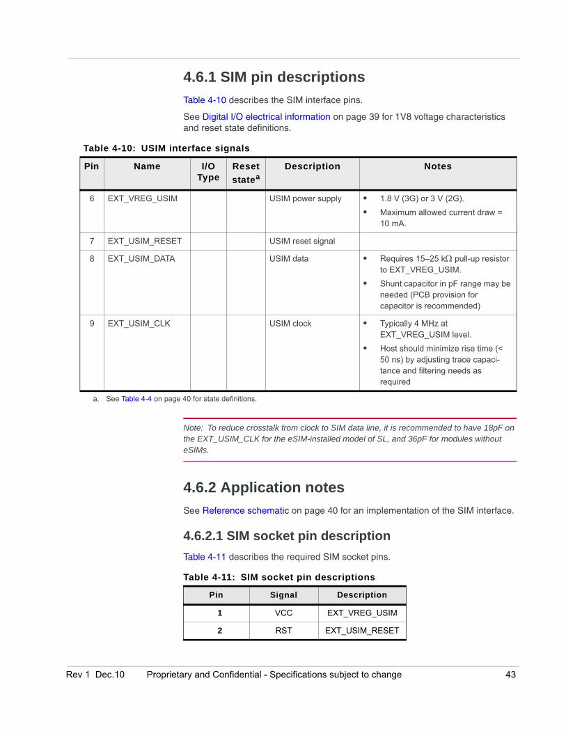
Table 4-10 describes the SIM interface pins.
See Digital I/O electrical information on page 39 for 1V8 voltage characteristics and reset state definitions.
Note: To reduce crosstalk from clock to SIM data line, it is recommended to have 18pF on the EXT_USIM_CLK for the eSIM-installed model of SL, and 36pF for modules without eSIMs.
4.6.2 Application notes
See Reference schematic on page 40 for an implementation of the SIM interface.
4.6.2.1 SIM socket pin description
Table 4-11 describes the required SIM socket pins.
Table 4-10: USIM interface signals
Pin Name I/O Type
Reset
stateaDescription Notes
6 EXT_VREG_USIM USIM power supply • 1.8 V (3G) or 3 V (2G).
• Maximum allowed current draw = 10 mA.
7 EXT_USIM_RESET USIM reset signal
8 EXT_USIM_DATA USIM data • Requires 15–25 k pull-up resistor to EXT_VREG_USIM.
• Shunt capacitor in pF range may be needed (PCB provision for capacitor is recommended)
9 EXT_USIM_CLK USIM clock • Typically 4 MHz at EXT_VREG_USIM level.
• Host should minimize rise time (< 50 ns) by adjusting trace capaci-tance and filtering needs as required
a. See Table 4-4 on page 40 for state definitions.
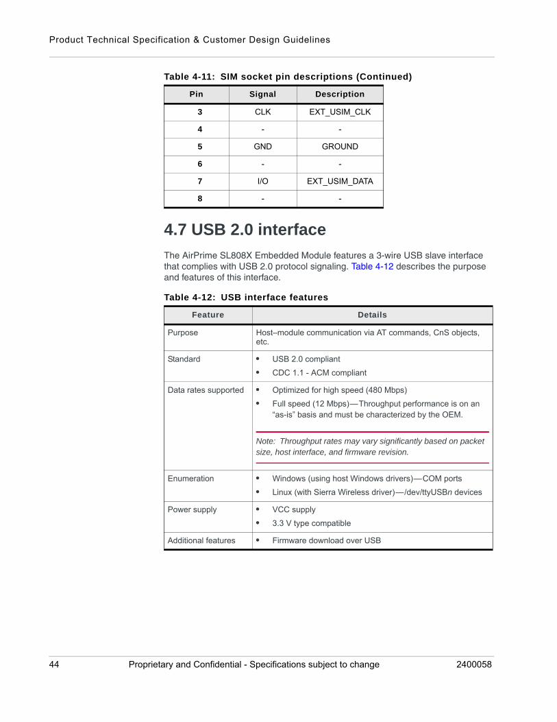
Table 4-11: SIM socket pin descriptions
Pin Signal Description
1 VCC EXT_VREG_USIM
2 RST EXT_USIM_RESET
Rev 1 Dec.10 Proprietary and Confidential - Specifications subject to change 43
Product Technical Specification & Customer Design Guidelines
4.7 USB 2.0 interface
The AirPrime SL808X Embedded Module features a 3-wire USB slave interface that complies with USB 2.0 protocol signaling. Table 4-12 describes the purpose and features of this interface.
3 CLK EXT_USIM_CLK
4 - -
5 GND GROUND
6 - -
7 I/O EXT_USIM_DATA
8 - -
Table 4-12: USB interface features
Feature Details
Purpose Host–module communication via AT commands, CnS objects, etc.
Standard • USB 2.0 compliant
• CDC 1.1 - ACM compliant
Data rates supported • Optimized for high speed (480 Mbps)
• Full speed (12 Mbps)—Throughput performance is on an “as-is” basis and must be characterized by the OEM.
Note: Throughput rates may vary significantly based on packet size, host interface, and firmware revision.
Enumeration • Windows (using host Windows drivers)—COM ports
• Linux (with Sierra Wireless driver)—/dev/ttyUSBn devices
Power supply • VCC supply
• 3.3 V type compatible
Additional features • Firmware download over USB
Table 4-11: SIM socket pin descriptions (Continued)
Pin Signal Description
44 Proprietary and Confidential - Specifications subject to change 2400058
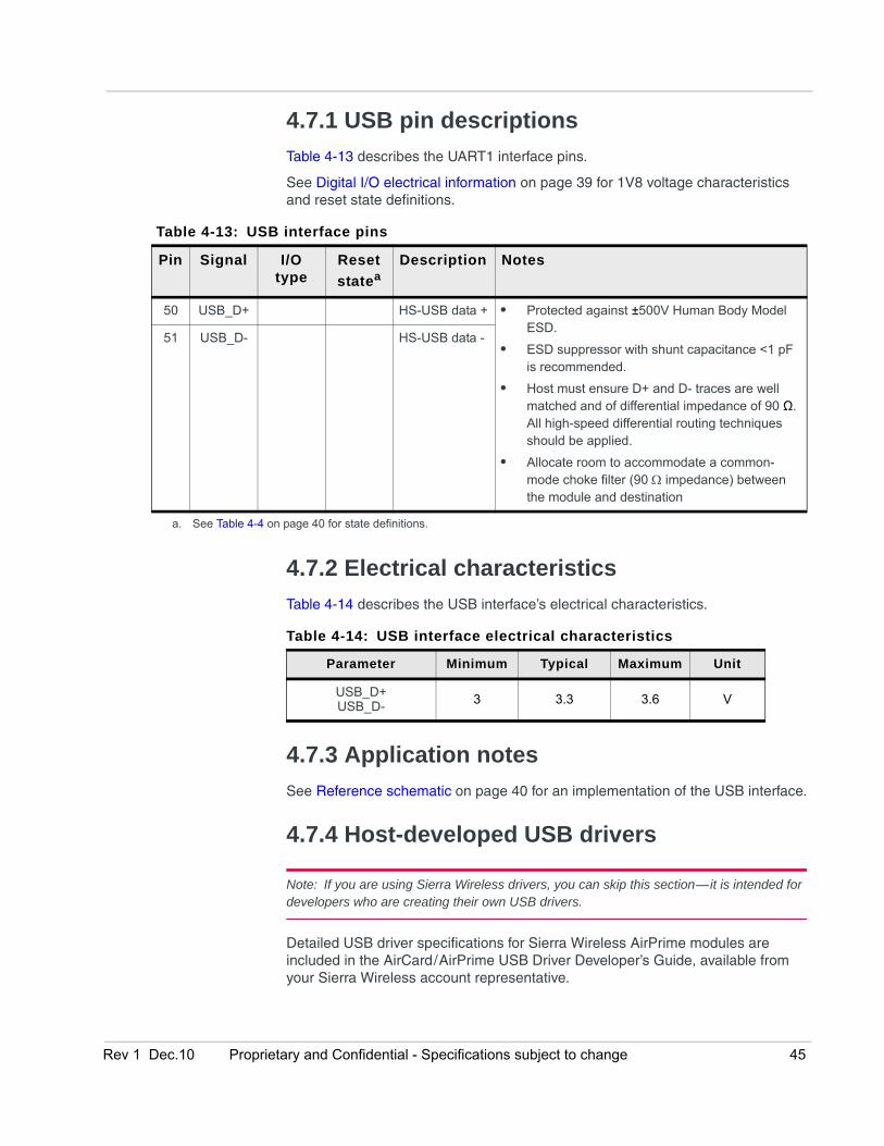
4.7.1 USB pin descriptions
Table 4-13 describes the UART1 interface pins.
See Digital I/O electrical information on page 39 for 1V8 voltage characteristics and reset state definitions.
4.7.2 Electrical characteristics
Table 4-14 describes the USB interface’s electrical characteristics.
4.7.3 Application notes
See Reference schematic on page 40 for an implementation of the USB interface.
4.7.4 Host-developed USB drivers
Note: If you are using Sierra Wireless drivers, you can skip this section—it is intended for developers who are creating their own USB drivers.
Detailed USB driver specifications for Sierra Wireless AirPrime modules are included in the AirCard/AirPrime USB Driver Developer’s Guide, available from your Sierra Wireless account representative.
Table 4-13: USB interface pins
Pin Signal I/O type
Reset
stateaDescription Notes
50 USB_D+ HS-USB data + • Protected against ±500V Human Body Model ESD.
• ESD suppressor with shunt capacitance <1 pF is recommended.
• Host must ensure D+ and D- traces are well matched and of differential impedance of 90 Ω. All high-speed differential routing techniques should be applied.
• Allocate room to accommodate a common-mode choke filter (90 impedance) between the module and destination
51 USB_D- HS-USB data -
a. See Table 4-4 on page 40 for state definitions.
Table 4-14: USB interface electrical characteristics
Parameter Minimum Typical Maximum Unit
USB_D+USB_D- 3 3.3 3.6 V
Rev 1 Dec.10 Proprietary and Confidential - Specifications subject to change 45
Product Technical Specification & Customer Design Guidelines
4.7.4.1 Supported architectures
The AirPrime SL808X Embedded Module supports the following architectures over the USB interface on Windows, Windows CE, and Linux systems:
• Sierra Wireless Direct IP—Composite USB
• Non-MUX—Composite USB
• MUX (3GPP 27.010)—Composite USB (The MUX architecture is also available over the UART interface.)
• Non-MUX—Non-composite USB
For design requirements, see [6] AirCard/AirPrime USB Driver Developer’s Guide.
The basic service configuration is PRI-dependent and may include the NDIS, AT, and CnS services. The advanced service configuration (available for Windows and Windows CE) is disabled by default, and may include the DM and PDP services.
4.7.4.2 USB driver requirements
The host USB driver must meet each of these requirements:
• Must act as a USB host device to interface with the module.
• Must support remote wakeup, resume, and suspend operations as described in Universal Serial Bus Specification, Rev 2.0, and USB Suspend mode on page 46 and USB Resume mode on page 46.
• Must support serial port emulation. The module implements both 27.010 multiplexing and USB-CDC.
• Should NOT send any SOF tokens (start-of-frames) to the module when there is no valid data to send. These tokens keep the module awake and cause unnecessary power consumption.
4.7.5 USB Suspend mode
When the module enters suspend mode, it shuts down the USB clock to save power.
While in the suspend state:
• Module provides signalling on the USB interface (USB_D+/USB_D-) to indicate its current state to the host device.
• VCC_3V6 must be maintained.
4.7.6 USB Resume mode
USB activity may be resumed by either the USB host or by the module:
• Host-initiated:
a. USB transceiver detects the change in bus activity and triggers the USB_RESUME interrupt to the module's processor.
b. Module enables its USB clock and responds to the host.
46 Proprietary and Confidential - Specifications subject to change 2400058
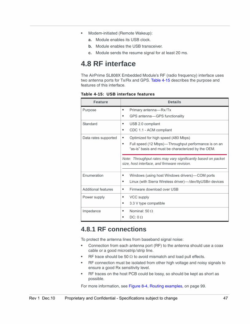
• Modem-initiated (Remote Wakeup):
a. Module enables its USB clock.
b. Module enables the USB transceiver.
c. Module sends the resume signal for at least 20 ms.
4.8 RF interface
The AirPrime SL808X Embedded Module’s RF (radio frequency) interface uses two antenna ports for Tx/Rx and GPS. Table 4-15 describes the purpose and features of this interface.
4.8.1 RF connections
To protect the antenna lines from baseband signal noise:
• Connection from each antenna port (RF) to the antenna should use a coax cable or a good microstrip/strip line.
• RF trace should be 50 to avoid mismatch and load pull effects.
• RF connection must be isolated from other high voltage and noisy signals to ensure a good Rx sensitivity level.
• RF traces on the host PCB could be lossy, so should be kept as short as possible.
For more information, see Figure 8-4, Routing examples, on page 99.
Table 4-15: USB interface features
Feature Details
Purpose • Primary antenna—Rx/Tx
• GPS antenna—GPS functionality
Standard • USB 2.0 compliant
• CDC 1.1 - ACM compliant
Data rates supported • Optimized for high speed (480 Mbps)
• Full speed (12 Mbps)—Throughput performance is on an “as-is” basis and must be characterized by the OEM.
Note: Throughput rates may vary significantly based on packet size, host interface, and firmware revision.
Enumeration • Windows (using host Windows drivers)—COM ports
• Linux (with Sierra Wireless driver)—/dev/ttyUSBn devices
Additional features • Firmware download over USB
Power supply • VCC supply
• 3.3 V type compatible
Impedance • Nominal: 50
• DC: 0
Rev 1 Dec.10 Proprietary and Confidential - Specifications subject to change 47
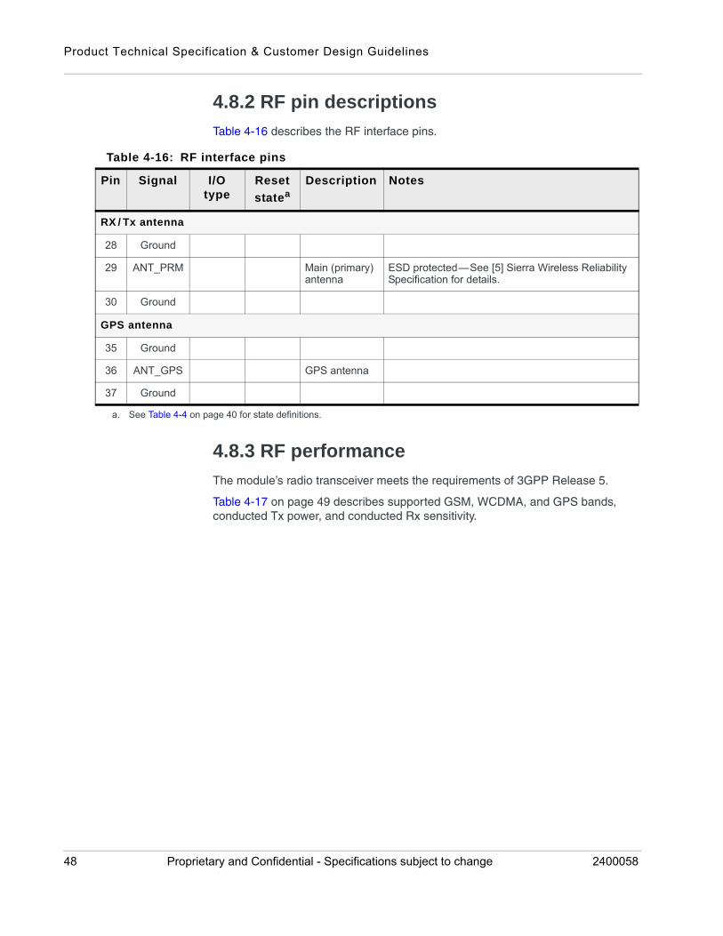
Product Technical Specification & Customer Design Guidelines
4.8.2 RF pin descriptions
Table 4-16 describes the RF interface pins.
4.8.3 RF performance
The module’s radio transceiver meets the requirements of 3GPP Release 5.
Table 4-17 on page 49 describes supported GSM, WCDMA, and GPS bands, conducted Tx power, and conducted Rx sensitivity.
Table 4-16: RF interface pins
Pin Signal I/O type
Reset
stateaDescription Notes
RX / Tx antenna
28 Ground
29 ANT_PRM Main (primary) antenna
ESD protected—See [5] Sierra Wireless Reliability Specification for details.
30 Ground
GPS antenna
35 Ground
36 ANT_GPS GPS antenna
37 Ground
a. See Table 4-4 on page 40 for state definitions.
48 Proprietary and Confidential - Specifications subject to change 2400058
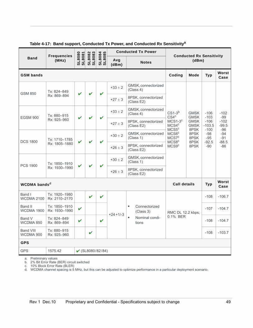
GS
GSM
EGS
DCS
PCS
WC
BanWC
BanWC
BanWC
BanWC
GP
GPS
abcd
Table 4-17: Band support, Conducted Tx Power, and Conducted Rx Sensitivitya
BandFrequencies
(MHz)
SL
80
80
SL
80
81
SL
80
82
SL
80
83
SL
80
84
SL
80
85 Conducted Tx Power
Conducted Rx Sensitivity (dBm)Avg
(dBm)Notes
M bands Coding Mode TypWorstCase
850 Tx: 824–849Rx: 869–894
+33 2GMSK, connectorized (Class 4)
CS1-3b
CS4c
MCS1-3c
MCS4c
MCS5c
MCS6c
MCS7c
MCS8c
MCS9c
GMSKGMSKGMSKGMSK8PSK8PSK8PSK8PSK8PSK
-106-103-106
-103.5-100-98-95
-92.5-90
-102-99
-102-99.5-96-94-91
-88.5-86
+27 3 8PSK, connectorized (Class E2)
M 900 Tx: 880–915Rx: 925–960
+33 2 GMSK, connectorized (Class 4)
+27 38PSK, connectorized (Class E2)
1800Tx: 1710–1785Rx: 1805–1880
+30 2 GMSK, connectorized (Class 1)
+26 3 8PSK, connectorized (Class E2)
1900 Tx: 1850–1910Rx: 1930–1990
+30 2GMSK, connectorized (Class 1)
+26 3 8PSK, connectorized (Class E2)
DMA bandsd Call details TypWorstCase
d IDMA 2100
Tx: 1920–1980Rx: 2110–2170
+24 +1/-3
• Connectorized (Class 3)
• Nominal condi-tions
RMC DL 12.2 kbps;0.1% BER
-108 -106.7
d IIDMA 1900
Tx: 1850–1910Rx: 1930–1990 -107 -104.7
d VDMA 850
Tx: 824–849Rx: 869–894 -108 -104.7
d VIIIDMA 900
Tx: 880–915Rx: 925–960
-108 -103.7
S
1575.42 (SL8080/82/84)
. Preliminary values
. 2% Bit Error Rate (BER) circuit switched
. 10% Block Error Rate (BLER)
. WCDMA channel spacing is 5 MHz, but this can be adjusted to optimize performance in a particular deployment scenario.
Rev 1 Dec.10 Proprietary and Confidential - Specifications subject to change 49
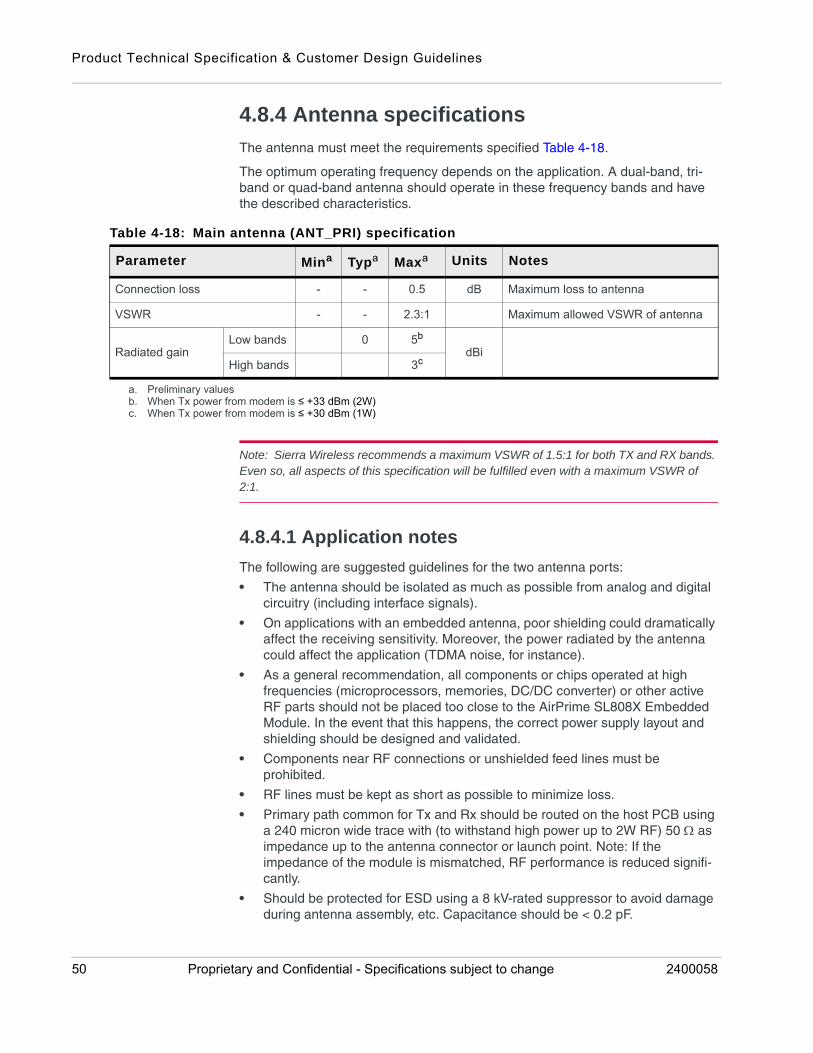
Product Technical Specification & Customer Design Guidelines
4.8.4 Antenna specifications
The antenna must meet the requirements specified Table 4-18.
The optimum operating frequency depends on the application. A dual-band, tri-band or quad-band antenna should operate in these frequency bands and have the described characteristics.
Note: Sierra Wireless recommends a maximum VSWR of 1.5:1 for both TX and RX bands. Even so, all aspects of this specification will be fulfilled even with a maximum VSWR of 2:1.
4.8.4.1 Application notes
The following are suggested guidelines for the two antenna ports:
• The antenna should be isolated as much as possible from analog and digital circuitry (including interface signals).
• On applications with an embedded antenna, poor shielding could dramatically affect the receiving sensitivity. Moreover, the power radiated by the antenna could affect the application (TDMA noise, for instance).
• As a general recommendation, all components or chips operated at high frequencies (microprocessors, memories, DC/DC converter) or other active RF parts should not be placed too close to the AirPrime SL808X Embedded Module. In the event that this happens, the correct power supply layout and shielding should be designed and validated.
• Components near RF connections or unshielded feed lines must be prohibited.
• RF lines must be kept as short as possible to minimize loss.
• Primary path common for Tx and Rx should be routed on the host PCB using a 240 micron wide trace with (to withstand high power up to 2W RF) 50 as impedance up to the antenna connector or launch point. Note: If the impedance of the module is mismatched, RF performance is reduced signifi-cantly.
• Should be protected for ESD using a 8 kV-rated suppressor to avoid damage during antenna assembly, etc. Capacitance should be < 0.2 pF.
Table 4-18: Main antenna (ANT_PRI) specification
Parameter Mina Typa Maxa Units Notes
Connection loss - - 0.5 dB Maximum loss to antenna
VSWR - - 2.3:1 Maximum allowed VSWR of antenna
Radiated gainLow bands 0 5b
dBiHigh bands 3c
a. Preliminary valuesb. When Tx power from modem is ≤ +33 dBm (2W)c. When Tx power from modem is ≤ +30 dBm (1W)
50 Proprietary and Confidential - Specifications subject to change 2400058
• RF trace and cable connecting the pin to the antenna should be of low loss (<0.3 dB)
• Antenna connected on the ANT_PRM port should offer 2:1 or better VSWR in order to maintain Tx power within +/- 2dB from the nominal power and the VSWR could be 2.3:1 or better for the Rx band frequencies.
• Antenna connected on the ANT_GPS port should offer 3:1 or better VSWR in order to maintain radiated sensitivity.
• Antenna location may affect RF performance. Although the module is shielded to prevent interference in most applications, the placement of the antenna is still very important—if the host device is insufficiently shielded, high levels of broadband or spurious noise can degrade the module’s perfor-mance.
• Antenna cables should be routed, if possible, away from noise sources (switching power supplies, LCD assemblies, etc.). If the cables are near the noise sources, the noise may be coupled into the RF cable and into the antenna.
4.8.5 Radiated emissions
The device alone meets all regulatory emissions limits when tested into a cabled (conducted) 50 system. With antenna designs with up to 2.3:1 VSWR or worse, the radiated emissions could exceed limits. These emissions must be tested with the final antenna to ensure they pass. Examples of these limits would be FCC Part 22 and Part 24, test case 12.2.1 for GSM (3GPP TS 51.010), and test case 4.2.2 for WCDMA (ETSI EN 301 511).
The system gain value affects both radiated power and regulatory (FCC, IC, CE, etc.) test results.
4.8.6 Radiated sensitivity measurement
A wireless device contains many sources of noise that contribute to a reduction in Rx performance.
To determine the extent of any desensitization of receiver performance due to self-generated noise in the host device, over-the-air (OTA) or radiated testing is required. This testing can be performed by Sierra Wireless or you can use your own OTA test chamber for in-house testing.
Most carriers require a certain level of receiver performance to ensure proper functioning of the device on their networks. Although AirPrime soldered-down modules have been designed to meet these carrier requirements, they are still susceptible to various performance inhibitors.
4.9 Audio interfaces
The AirPrime SL808X Embedded Module supports two audio interfaces (analog and PCM digital) and allows dynamic run-time selection of the appropriate interface:
• Analog audio interface on page 52
• Digital audio interface (PCM) on page 62
Rev 1 Dec.10 Proprietary and Confidential - Specifications subject to change 51
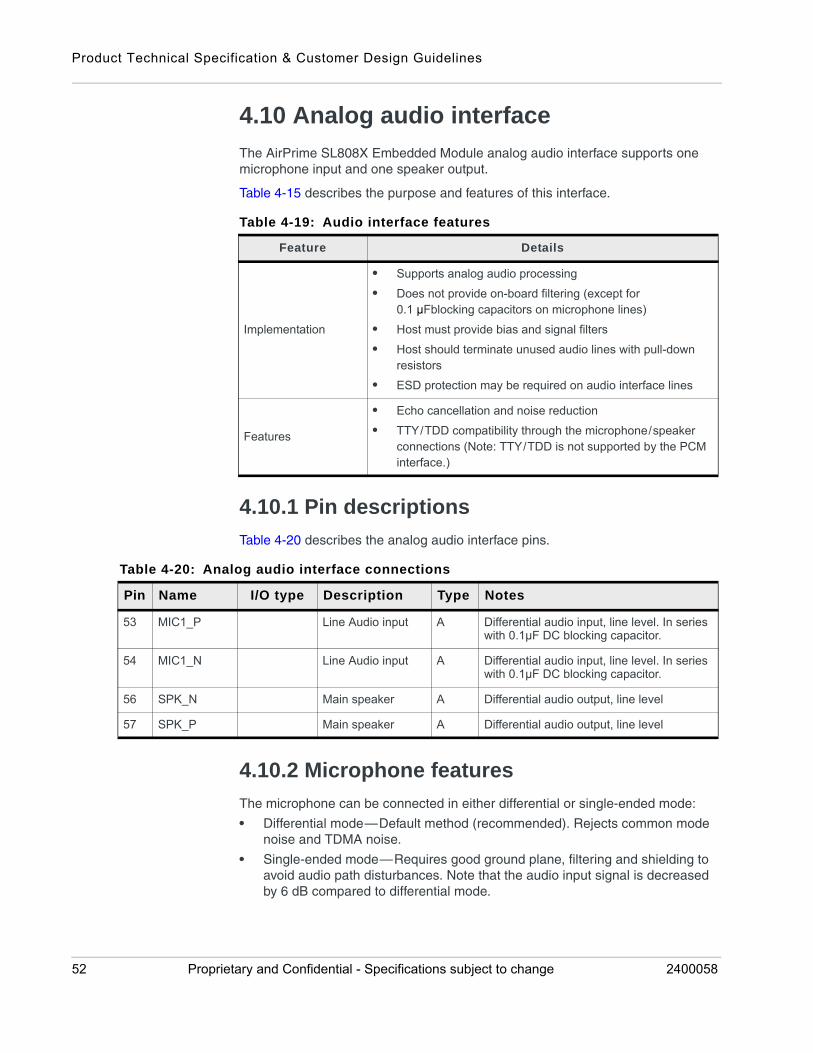
Product Technical Specification & Customer Design Guidelines
4.10 Analog audio interface
The AirPrime SL808X Embedded Module analog audio interface supports one microphone input and one speaker output.
Table 4-15 describes the purpose and features of this interface.
4.10.1 Pin descriptions
Table 4-20 describes the analog audio interface pins.
4.10.2 Microphone features
The microphone can be connected in either differential or single-ended mode:
• Differential mode—Default method (recommended). Rejects common mode noise and TDMA noise.
• Single-ended mode—Requires good ground plane, filtering and shielding to avoid audio path disturbances. Note that the audio input signal is decreased by 6 dB compared to differential mode.
Table 4-19: Audio interface features
Feature Details
Implementation
• Supports analog audio processing
• Does not provide on-board filtering (except for 0.1 µFblocking capacitors on microphone lines)
• Host must provide bias and signal filters
• Host should terminate unused audio lines with pull-down resistors
• ESD protection may be required on audio interface lines
Features
• Echo cancellation and noise reduction
• TTY/TDD compatibility through the microphone/speaker connections (Note: TTY/TDD is not supported by the PCM interface.)
Table 4-20: Analog audio interface connections
Pin Name I/O type Description Type Notes
53 MIC1_P Line Audio input A Differential audio input, line level. In series with 0.1µF DC blocking capacitor.
54 MIC1_N Line Audio input A Differential audio input, line level. In series with 0.1µF DC blocking capacitor.
56 SPK_N Main speaker A Differential audio output, line level
57 SPK_P Main speaker A Differential audio output, line level
52 Proprietary and Confidential - Specifications subject to change 2400058
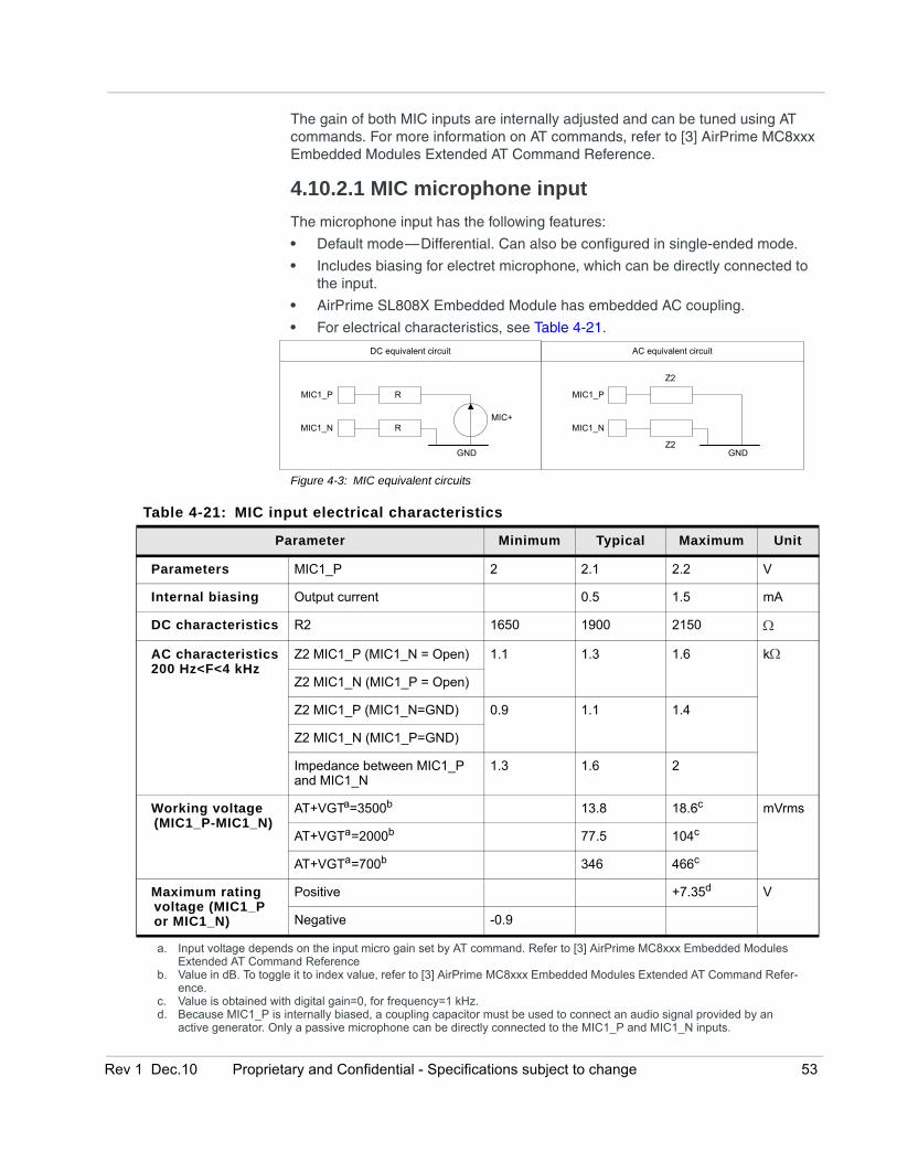
The gain of both MIC inputs are internally adjusted and can be tuned using AT commands. For more information on AT commands, refer to [3] AirPrime MC8xxx Embedded Modules Extended AT Command Reference.
4.10.2.1 MIC microphone input
The microphone input has the following features:
• Default mode—Differential. Can also be configured in single-ended mode.
• Includes biasing for electret microphone, which can be directly connected to the input.
• AirPrime SL808X Embedded Module has embedded AC coupling.
• For electrical characteristics, see Table 4-21.
Figure 4-3: MIC equivalent circuits
R
R
MIC1_P
MIC1_NMIC+
GND
Z2
MIC1_P
MIC1_N
GNDZ2
DC equivalent circuit AC equivalent circuit
Table 4-21: MIC input electrical characteristics
Parameter Minimum Typical Maximum Unit
Parameters MIC1_P 2 2.1 2.2 V
Internal biasing Output current 0.5 1.5 mA
DC characteristics R2 1650 1900 2150
AC characteristics200 Hz<F<4 kHz
Z2 MIC1_P (MIC1_N = Open) 1.1 1.3 1.6 k
Z2 MIC1_N (MIC1_P = Open)
Z2 MIC1_P (MIC1_N=GND) 0.9 1.1 1.4
Z2 MIC1_N (MIC1_P=GND)
Impedance between MIC1_P and MIC1_N
1.3 1.6 2
Working voltage (MIC1_P-MIC1_N)
AT+VGTa=3500b 13.8 18.6c mVrms
AT+VGTa=2000b 77.5 104c
AT+VGTa=700b 346 466c
Maximum rating voltage (MIC1_P or MIC1_N)
Positive +7.35d V
Negative -0.9
a. Input voltage depends on the input micro gain set by AT command. Refer to [3] AirPrime MC8xxx Embedded Modules Extended AT Command Reference
b. Value in dB. To toggle it to index value, refer to [3] AirPrime MC8xxx Embedded Modules Extended AT Command Refer-ence.
c. Value is obtained with digital gain=0, for frequency=1 kHz.d. Because MIC1_P is internally biased, a coupling capacitor must be used to connect an audio signal provided by an
active generator. Only a passive microphone can be directly connected to the MIC1_P and MIC1_N inputs.
Rev 1 Dec.10 Proprietary and Confidential - Specifications subject to change 53
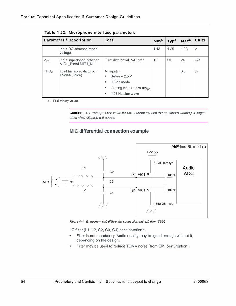
Product Technical Specification & Customer Design Guidelines
Caution: The voltage input value for MIC cannot exceed the maximum working voltage; otherwise, clipping will appear.
MIC differential connection example
Figure 4-4: Example—MIC differential connection with LC filter (TBD)
LC filter (L1, L2, C2, C3, C4) considerations:
• Filter is not mandatory. Audio quality may be good enough without it, depending on the design.
• Filter may be used to reduce TDMA noise (from EMI perturbation).
Table 4-22: Microphone interface parameters
Parameter / Description Test Mina Typa Maxa Units
Input DC common mode voltage
1.13 1.25 1.38 V
ZIn1 Input impedance between MIC1_P and MIC1_N
Fully differential, A/D path 16 20 24 k
THDV Total harmonic distortion +Noise (voice)
All inputs:
• AVDD = 2.5 V
• 13-bit mode
• analog input at 229 mVpp
• 498 Hz sine wave
3.5 %
a. Preliminary values
AirPrime SL module
Audio ADC
MIC C1
C2
C3
C4
L1
L2
S3
S4
MIC1_P
MIC1_N
1350 Ohm typ
100nF
100nF
1350 Ohm typ
1.2V typ
54 Proprietary and Confidential - Specifications subject to change 2400058
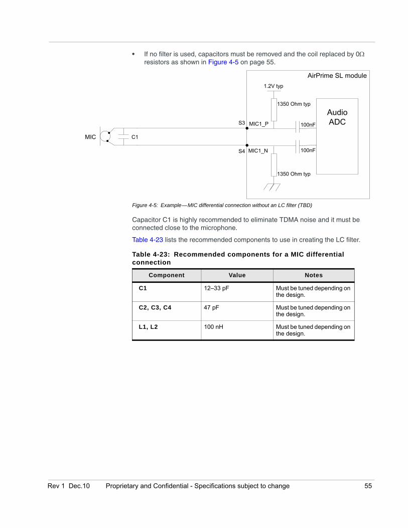
• If no filter is used, capacitors must be removed and the coil replaced by 0 resistors as shown in Figure 4-5 on page 55.
Figure 4-5: Example—MIC differential connection without an LC filter (TBD)
Capacitor C1 is highly recommended to eliminate TDMA noise and it must be connected close to the microphone.
Table 4-23 lists the recommended components to use in creating the LC filter.
AirPrime SL module
Audio ADC
MIC C1
S3
S4
MIC1_P
MIC1_N
1350 Ohm typ
100nF
100nF
1350 Ohm typ
1.2V typ
Table 4-23: Recommended components for a MIC differential connection
Component Value Notes
C1 12–33 pF Must be tuned depending on the design.
C2, C3, C4 47 pF Must be tuned depending on the design.
L1, L2 100 nH Must be tuned depending on the design.
Rev 1 Dec.10 Proprietary and Confidential - Specifications subject to change 55

Product Technical Specification & Customer Design Guidelines
MIC single-ended connection example
Figure 4-6: Example—MIC single-ended connection with LC filter (TBD)
Single-ended connection considerations:
• Not recommended for improving TDMA noise rejection as it is usually difficult to eliminate TDMA noise from a single-ended design.
• Internal input resistor value becomes 1150 due to the connection of MIC1_N to the ground.
• LC filter (L1 and C2) is recommended (but not mandatory) to eliminate TDMA noise. If the filter is not to be used, the capacitor C2 must be removed and the coil replaced by 0 resistors as shown in Figure 4-7 on page 56.
Figure 4-7: Example - MIC single-ended connection without an LC filter (TBD)
Capacitor C1 is highly recommended to eliminate TDMA noise and it must be connected close to the microphone.
AirPrime SL module
Audio ADC
MIC C1 C2
L1
S3
S4
MIC1_P
MIC1_N
1150 Ohm typ
100nF
100nF
1.2V typ
AirPrime SL module
Audio ADC
MIC C1
S3
S4
MIC1_P
MIC1_N
1150 Ohm typ
100nF
100nF
1.2V typ
56 Proprietary and Confidential - Specifications subject to change 2400058

Table 4-24 lists the recommended components to use in creating the LC filter.
4.10.3 Speaker features
The speaker can be connected in either differential or single-ended mode:
• Differential mode—Default method (recommended). Rejects common mode noise and TDMA noise.
• Single-ended mode—Requires good ground plane, filtering, and shielding to avoid audio path disturbances. Experiences power loss (power is divided by 4 in a single-ended connection) compared to differential connection.
The gain of each speaker output channel is internally adjusted and can be tuned using AT commands. For more information on AT commands, see [3] AirPrime MC8xxx Embedded Modules Extended AT Command Reference.
Discreet components (for example, resistors and capacitors) are not needed for this interface.
Table 4-25 lists the typical values of both speaker outputs.
4.10.3.1 Speakers output power
Because SPK can provide more power, it can be connected in differential mode. The maximal specifications given below are available with the maximum power output configuration values set by AT command, and the typical values are recommended.
Caution: It is mandatory not to exceed the maximal speaker output power and the speaker load must be in accordance with the gain selection (gain is controlled by AT command). Exceeding beyond the specified maximal output power may damage the AirPrime SL808X Embedded Module.
Table 4-24: Recommended components for a MIC single-ended connection
Component Value Notes
C1 12–33 pF Must be tuned depending on the design.
C2 Must be tuned depending on the design.
L1 Must be tuned depending on the design.
Table 4-25: Speaker information
Parameter Typical Unit Connection
Z (SPK_P, SPK_N) 4 Single-ended mode
Z (SPK_P, SPK_N) 8 Differential mode
Rev 1 Dec.10 Proprietary and Confidential - Specifications subject to change 57
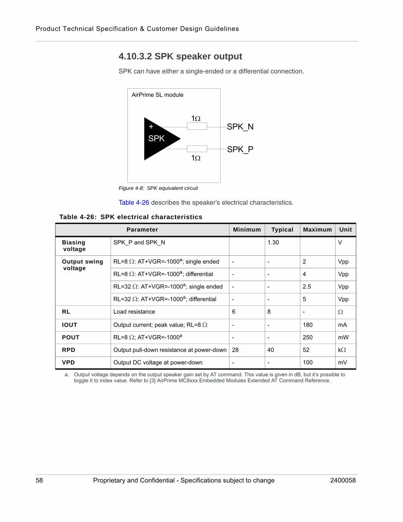
Product Technical Specification & Customer Design Guidelines
4.10.3.2 SPK speaker output
SPK can have either a single-ended or a differential connection.
Figure 4-8: SPK equivalent circuit
Table 4-26 describes the speaker’s electrical characteristics.
AirPrime SL module
SPK
+ SPK_N
SPK_P
1
1
Table 4-26: SPK electrical characteristics
Parameter Minimum Typical Maximum Unit
Biasing voltage
SPK_P and SPK_N 1.30 V
Output swing voltage
RL=8 : AT+VGR=-1000a; single ended - - 2 Vpp
RL=8 : AT+VGR=-1000a; differential - - 4 Vpp
RL=32 : AT+VGR=-1000a; single ended - - 2.5 Vpp
RL=32 : AT+VGR=-1000a; differential - - 5 Vpp
RL Load resistance 6 8 -
IOUT Output current; peak value; RL=8 - - 180 mA
POUT RL=8 ; AT+VGR=-1000a - - 250 mW
RPD Output pull-down resistance at power-down 28 40 52 k
VPD Output DC voltage at power-down - - 100 mV
a. Output voltage depends on the output speaker gain set by AT command. This value is given in dB, but it’s possible to toggle it to index value. Refer to [3] AirPrime MC8xxx Embedded Modules Extended AT Command Reference.
58 Proprietary and Confidential - Specifications subject to change 2400058
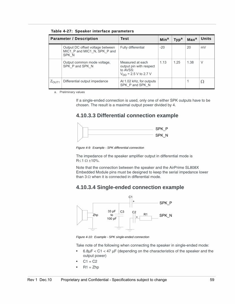
If a single-ended connection is used, only one of either SPK outputs have to be chosen. The result is a maximal output power divided by 4.
4.10.3.3 Differential connection example
Figure 4-9: Example - SPK differential connection
The impedance of the speaker amplifier output in differential mode is R1 10%.
Note that the connection between the speaker and the AirPrime SL808X Embedded Module pins must be designed to keep the serial impedance lower than 3 when it is connected in differential mode.
4.10.3.4 Single-ended connection example
Figure 4-10: Example - SPK single-ended connection
Take note of the following when connecting the speaker in single-ended mode:
• 6.8µF < C1 < 47 µF (depending on the characteristics of the speaker and the output power)
• C1 = C2
• R1 = Zhp
Table 4-27: Speaker interface parameters
Parameter / Description Test Mina Typa Maxa Units
Output DC offset voltage between MIC1_P and MIC1_N, SPK_P and SPK_N
Fully differential -20 20 mV
Output common mode voltage, SPK_P and SPK_N
Measured at each output pin with respect to AVSS:VDD = 2.5 V to 2.7 V
1.13 1.25 1.38 V
ZOUT1 Differential output impedance At 1.02 kHz, for outputs SPK_P and SPK_N
1
a. Preliminary values
SPK_P
SPK_N
SPK_P
SPK_NR1+
+
C2
C1
C333 pFto
100 pFZhp
Rev 1 Dec.10 Proprietary and Confidential - Specifications subject to change 59
Product Technical Specification & Customer Design Guidelines
Again, note that using a single-ended connection includes losing power (-6dB) as compared to a differential connection.
In the case of a 32 speaker, a cheaper and smaller solution can be implemented where R1 = 82 and C2 = 6.8µF (ceramic).
Also note that the connection between the speaker and the AirPrime SL808X Embedded Module pins must be designed to keep the serial impedance lower than 1.5 when it is connected in single-ended mode.
4.10.3.5 Recommended characteristics
• Type: 10 mW, electro-magnetic
• Impedance: 8 for hands-free
• Sensitivity: 110dB SPL minimum (0dB = 20 µPa)
• Frequency response must be compatible with GSM specifications
4.10.4 Supported voice features
The AirPrime SL808X Embedded Module modem supports the voice-related features listed in Table 4-28, and Table 4-29 details its support for supplementary services.
Table 4-28: Supported voice features
Item Comments
USSD (Unstructured Supplementary Services Data)
This is a GSM-specific capability that supports transmitting information over GSM network signalling channels.
Voice encryption Both A5/1 and A5/2 voice encryption are supported.
SIM Application Tool Kit with proactive SIM commands (compliant to R96)
3GPP TS 11.14SIM Application Toolkit commands are stored on the SIM. These commands enable the SIM card to proactively drive the GSM host device and support interactions between the network and the end user.
User-configurable audio prompts
Several audio features, such as ‘Incoming Call’ and ‘New SMS message’, can be configured in Watcher.
Multi-party calling Up to 5 remote parties are supported on a single call, plus an additional party on hold (on a separate call).
Table 4-29: Supported supplementary services
Supported by
Service Watcher / CnS
GSM service code
AT command
Calling Line Identification Presentation (Caller ID)
Yes Yes Yes
Calling LIne Identification Restriction (hides your ID on outgoing calls)
Yes Yes Yes
60 Proprietary and Confidential - Specifications subject to change 2400058
4.10.5 Short Message Service (SMS)
Table 4-30 summarizes the SL808X module’s compliance with specific SMS features:
4.10.6 UMTS radio access bearers supported
The SL808X modem supports the majority of the radio access bearers specified in 3GPP TS 34.108. If you require a detailed list, contact Sierra Wireless.
Call Waiting Yes Yes Yes
Call Hold Yes N/A (TBD) Yes
Multi-party service Yes N/A (TBD) Yes
Call Forwarding
Unconditional Yes Yes Yes
on Mobile Subscriber Busy Yes Yes Yes
on No Reply Yes Yes Yes
on Mobile Subscriber Not Reachable Yes Yes Yes
Call Barring
All outgoing calls Yes Yes Yes
Outgoing international calls Yes Yes Yes
Outgoing international calls (except those directed to the home PLMN country)
Yes Yes Yes
All incoming calls Yes Yes Yes
Incoming calls when roaming outside the home PLMN country
Yes Yes Yes
Table 4-29: Supported supplementary services (Continued)
Supported by
Service Watcher / CnS
GSM service code
AT command
Table 4-30: SMS features
Feature Supported
Mobile-terminated SMS
Mobile-originated SMS
Point-to-Point messaging
Cell Broadcast messaging
Rev 1 Dec.10 Proprietary and Confidential - Specifications subject to change 61
Product Technical Specification & Customer Design Guidelines
4.11 Digital audio interface (PCM)
The Digital Audio Interface (PCM) interface allows connectivity with standard audio peripherals. It can be used, for example, to connect an external audio codec. Table 4-31 describes the purpose and features of this interface.
The programmability of this interface allows addressing a large range of audio peripherals.
4.11.1 PCM pin descriptions
Table 4-32 describes the digital audio (PCM) interface pins.
See Digital I/O electrical information on page 39 for 1V8 voltage characteristics and reset state definitions.
Note: Note that the digital audio interface configuration cannot differ from this specifi-cation.
Table 4-31: PCM audio interface features
Feature Details
Implementation • Primary PCM supported to interface with external codec
Power • 1.8 V (use VREF_1V8 as logic reference)
Features
• IOM-2 compatible device on physical level
• Master mode only with 6 slots by frame (user only on slot 0)
• Bit rate single clock mode at 768 kHz only
• 16 bits data word MSB first only
• Linear Law only (no compression law)
• Long Frame Synchronization only
• Push-pull configuration on PCM_DOUT and PCM_DIN
Table 4-32: Audio pins
Pin Name I/O type Reset statea Description Notes
64 PCM_SYNC PCM synchronization bit • Delivers 8 kHz frequency pulse that synchronizes frame data in/out.
65 PCM_DOUT PCM output • Frame ‘data out’ relies on selected configuration mode.
66 PCM_DIN PCM input • Frame ‘data in’ relies on selected configuration mode.
67 PCM_CLK PCM clock • 2 MHz for primary PCM mode. Controls data transfer with the audio peripheral.
62 Proprietary and Confidential - Specifications subject to change 2400058
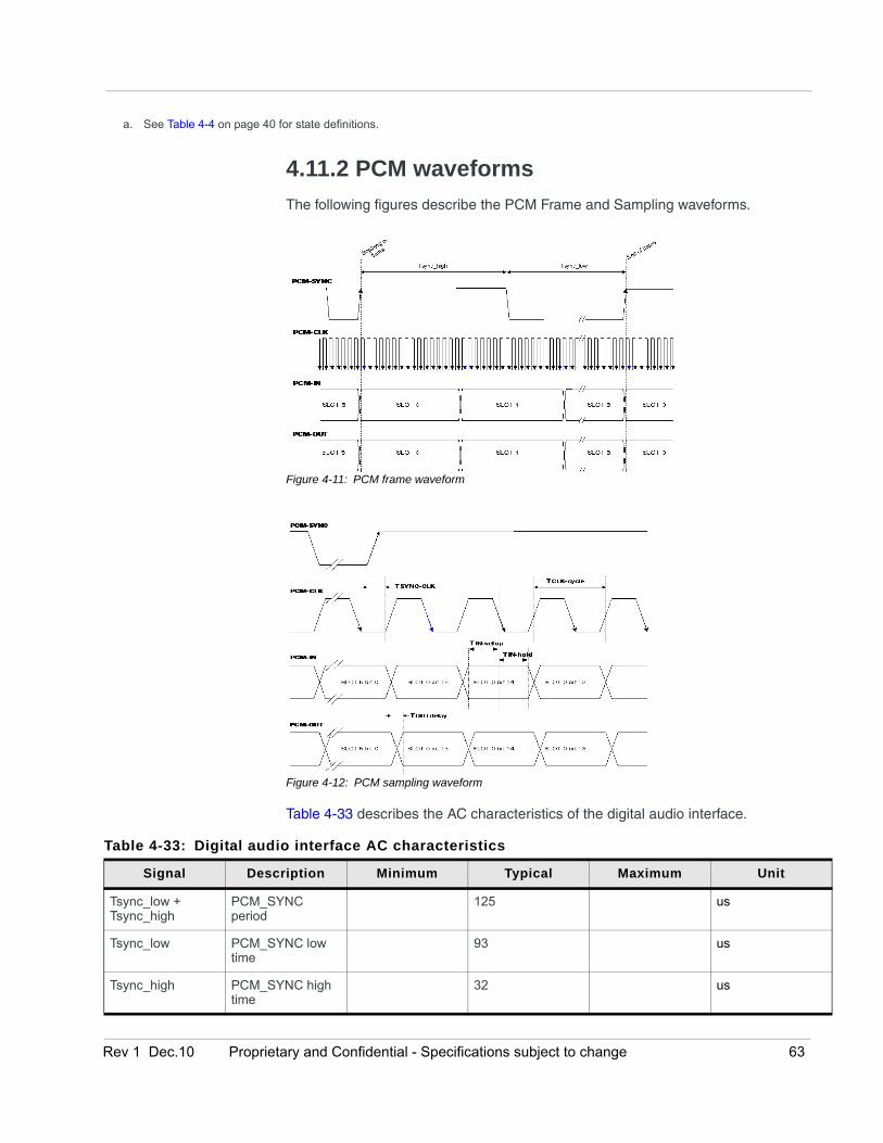
4.11.2 PCM waveforms
The following figures describe the PCM Frame and Sampling waveforms.
Figure 4-11: PCM frame waveform
Figure 4-12: PCM sampling waveform
Table 4-33 describes the AC characteristics of the digital audio interface.
a. See Table 4-4 on page 40 for state definitions.
Table 4-33: Digital audio interface AC characteristics
Signal Description Minimum Typical Maximum Unit
Tsync_low + Tsync_high
PCM_SYNC period
125 us
Tsync_low PCM_SYNC low time
93 us
Tsync_high PCM_SYNC high time
32 us
Rev 1 Dec.10 Proprietary and Confidential - Specifications subject to change 63

Product Technical Specification & Customer Design Guidelines
4.12 JTAG interface
The AirPrime SL808X Embedded Module includes a six-wire JTAG interface.
A six-wire JTAG ZIF connector may be installed to allow Sierra Wireless to use the interface for debugging/testing. (See JTAG connector on page 117 for recommended suppliers.)
If platform issues arise, contact Sierra Wireless for assistance.
TSYNC_CLK PCM_SYNC to PCM_CLK time
-154 ns
TCLK-cycle PCM_CLK period 1302 ns
TIN-setup PCM_DIN setup time
50 ns
TIN-hold PCM_DIN hold time
50 ns
TOUT-delay PCM_DOUT delay time
20 ns
Table 4-33: Digital audio interface AC characteristics (Continued)
Signal Description Minimum Typical Maximum Unit
64 Proprietary and Confidential - Specifications subject to change 2400058
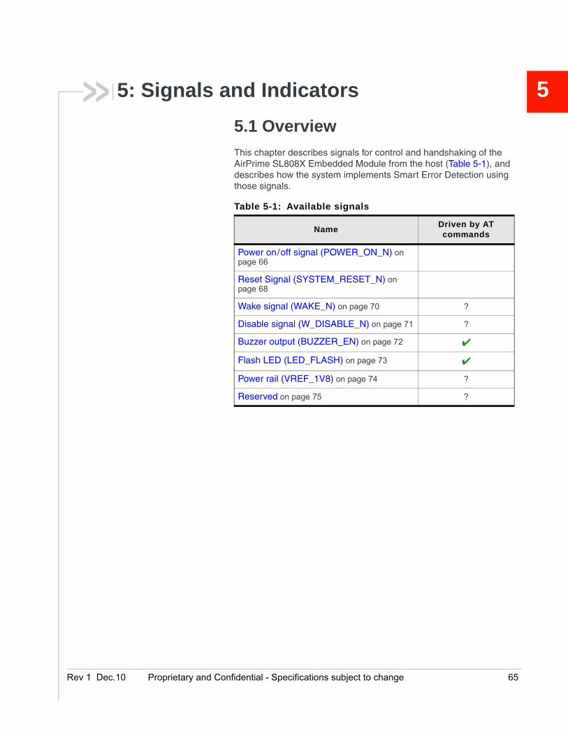
Rev 1 Dec
5
5: Signals and Indicators5.1 Overview
This chapter describes signals for control and handshaking of the AirPrime SL808X Embedded Module from the host (Table 5-1), and describes how the system implements Smart Error Detection using those signals.
Table 5-1: Available signals
NameDriven by AT commands
Power on/off signal (POWER_ON_N) on page 66
Reset Signal (SYSTEM_RESET_N) on page 68
Wake signal (WAKE_N) on page 70 ?
Disable signal (W_DISABLE_N) on page 71 ?
Buzzer output (BUZZER_EN) on page 72
Flash LED (LED_FLASH) on page 73
Power rail (VREF_1V8) on page 74 ?
Reserved on page 75 ?
.10 Proprietary and Confidential - Specifications subject to change 65
Product Technical Specification & Customer Design Guidelines
5.2 Power on/off signal (POWER_ON_N)
This signal is used to switch the AirPrime SL808X Embedded Module ON or OFF.
5.2.1 Pin descriptions
Table 5-3 describes the POWER_ON_N signal pins.
See Digital I/O electrical information on page 39 for 1V8 voltage characteristics and reset state definitions.
5.2.2 Electrical characteristics
Caution: All external signals must be inactive when the AirPrime SL808X Embedded Module is OFF to avoid any damage when starting and to allow the embedded module to start and stop correctly.
Refer to Table 4-2 on page 34 for basic characteristics (type, voltage).
5.2.3 Application notes
Caution: This section is under review and subject to change.
5.2.3.1 Procedure: Power on/off
To power on the modem, the host must:
1. Apply input voltage within valid range to power-supply pins. (See Table 3-1 on page 25 for Vcc range.)
Table 5-2: Power signal features
Feature Details
Purpose Power on/off
• Simulates a power button.
Implementation • Low = On
• Digital input
• Line should be driven only by an open-drain output from the host
• Level is internally pulled up to 2.6 V
Table 5-3: ON/~OFF signal pin description
Pin Signal I/O I/O type Description
43 POWER_ON_N I CMOS Embedded module power-on
66 Proprietary and Confidential - Specifications subject to change 2400058
2. Wait at least 50 ms, then assert POWER_ON_N (active low) for at least 400 ms to turn on the module.
3. Release the POWER_ON_N signal (module has internal pull-up to 2.6 V). Module is now in the ‘on’ (normal) power state.
To power off the modem, the host must:
1. Drive the signal low for at least 500 ms in order to initiate the power-down sequence, and then release it. (The modem continually monitors POWER_ON_N.)The module should now be in the ‘off’ power state.
Rev 1 Dec.10 Proprietary and Confidential - Specifications subject to change 67
Product Technical Specification & Customer Design Guidelines
5.3 Reset Signal (SYSTEM_RESET_N)
This signal is used to force the AirPrime SL808X Embedded Module to reset.
Note that an operating system reset is preferred to a hardware reset.
Caution: This signal should only be used for EMERGENCY resets.
5.3.1 Pin descriptions
Table 5-5 describes the SYSTEM_RESET_N signal pin.
See Digital I/O electrical information on page 39 for1V8 voltage characteristics and reset state definitions.
5.3.2 Electrical characteristics
Table 5-6 describes the reset signal’s electrical characteristics.
Refer to Table 4-2 on page 34 for basic characteristics (type, voltage).
Table 5-4: Reset signal features
Feature Details
Purpose Reset modem
• Used by host to reset the modem.
Implementation • Digital input. 1.8 V logic
• Signal is driven only by an open-drain output from the host.
• Host must provide a 50-100 k external pull-up resistor to 1.8 V.
Note: This pin is also required for JTAG programming.
Table 5-5: Reset signal pin description
Pin Signal I/O I/O type Description
63 SYSTEM_RESET_N I 1V8 Embedded module reset
Table 5-6: Reset signal electrical characteristics
Parameter Minimum Typical Maximum Unit
Input impedance (R)a 100 k
Input impedance (C) 10n F
SYSTEM_RESET_N time (Rt)b
200 us
68 Proprietary and Confidential - Specifications subject to change 2400058
5.3.3 Application notes
Caution: This section is under review and subject to change.
5.3.3.1 Reset sequence
To reset the modem (force the baseband circuit to reset):
1. Host drives signal low for 10–30 ms.
Note: Driving the signal low for a longer period will not damage the module, but will delay the reset process—the baseband circuit needs the line to be high at the end of the reset stage.
5.3.3.2 General notes
• This reset line should not be driven unless the host needs to enforce a baseband reset by asserting a logic low.
• An open collector or open drain transistor can be used. If an open collector is chosen, T1 can be a ROHM DTC144EE.
SYSTEM_RESET_N time (Rt)c at power up only
20 40 100 ms
Cancellation time (Ct) 34 ms
VHd 0.57 V
VIL 0 0.57 V
VIH 1.33 V
a. Internal pull-upb. This reset time is the minimum to be carried out on the SYSTEM_RESET_N signal when
the power supply is already stabilized.c. This reset time is internally carried out by the embedded module power supply supervisor
only when the embedded module power supplies are powered ON.d. VH: Hysterisis voltage
Table 5-7: Reset settings
Reset command SYSTEM_RESET_N (Pin 63)
Operating mode
1 0 Reset activated
0 1 Reset inactive
Table 5-6: Reset signal electrical characteristics
Parameter Minimum Typical Maximum Unit
Rev 1 Dec.10 Proprietary and Confidential - Specifications subject to change 69
Product Technical Specification & Customer Design Guidelines
5.4 Wake signal (WAKE_N)
This signal is used by the AirPrime SL808X Embedded Module to wake the host when a predetermined condition is satisfied (such as when a call is received).
5.4.1 Pin descriptions
Table 5-9 describes the wake signal pin.
See Digital I/O electrical information on page 39 for 1V8 voltage characteristics and reset state definitions.
5.4.2 Electrical characteristics
Refer to Table 4-2 on page 34 for basic characteristics (type, voltage).
Table 5-8: Wake signal features
Feature Details
Purpose Wake Host interface
• Wake host when a predetermined condition is satisfied (for example, when a call is received).
Implementation • Low = On
• Active low, 1.8 V logic.
• During the powered-off state, this pin may not be in a high impedance state. The host side must implement appropriate measures to accomodate this.
Table 5-9: Wake signal pin description
Pin Signal I/O I/O type Description
61 WAKE_N Wake Host interface
70 Proprietary and Confidential - Specifications subject to change 2400058

5.5 Disable signal (W_DISABLE_N)
This signal is used by the host to disable (or enable) the AirPrime SL808X Embedded Module’s RF connection.
5.5.1 Pin descriptions
Table 5-11 describes the wireless disable signal pin.
See Digital I/O electrical information on page 39 for 1V8 voltage characteristics and reset state definitions.
5.5.2 Electrical characteristics
Refer to Table 4-2 on page 34 for basic characteristics (type, voltage).
5.5.3 Application notes
Caution: This section is under review and subject to change.
5.5.3.1 Procedure: Disable/enable radio
To disable the RF connection:
1. Host asserts W_DISABLE_N.
To enable the RF connection (when in RF-disabled mode):
1. Host de-asserts W_DISABLE_N.
Table 5-10: Wireless Disable signal features
Feature Details
Purpose Wireless disable
• Used by host to disable or enable low power mode (‘airplane mode’).
Implementation • Low = Put module in airplane mode
• Digital input. Active low, 1.8 V logic.
• Host to provide a pull-up resistor of 50-100 k.
Table 5-11: Wireless disable signal pin description
Pin Signal I/O I/O type Description
62 W_DISABLE_N I Digital Wireless disable
Rev 1 Dec.10 Proprietary and Confidential - Specifications subject to change 71
Product Technical Specification & Customer Design Guidelines
5.6 Buzzer output (BUZZER_EN)
This signal is used in the implementation of a buzzer circuit.
5.6.1 Pin descriptions
Table 5-13 describes the wireless disable signal pin.
See Digital I/O electrical information on page 39 for 1V8 voltage characteristics and reset state definitions.
5.6.2 Electrical characteristics
Refer to Table 4-2 on page 34 for basic characteristics (type, voltage).
Table 5-12: Buzzer signal features
Feature Details
Purpose Enable off-board buzzer
Implementation • Binary I/O used by host as a buzzer enable line
Table 5-13: Buzzer output pin description
Pin Signal I/O I/O type Reset state
68 BUZZER_EN O Digital output Z
72 Proprietary and Confidential - Specifications subject to change 2400058
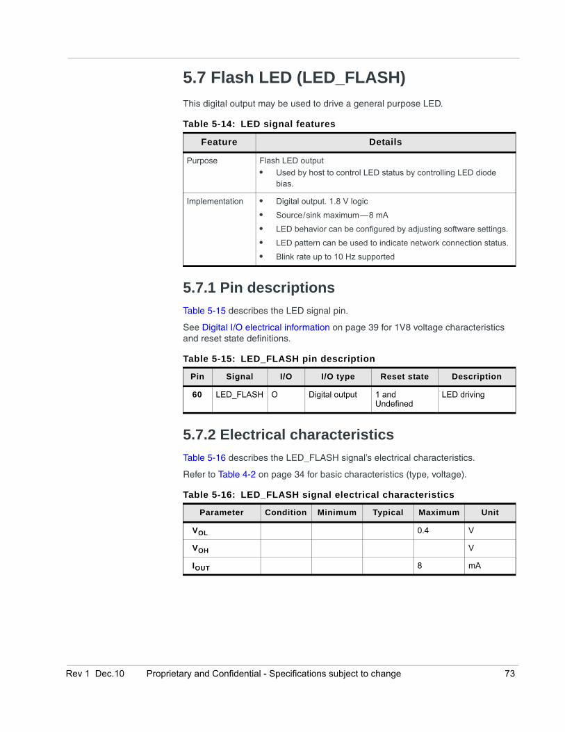
5.7 Flash LED (LED_FLASH)
This digital output may be used to drive a general purpose LED.
5.7.1 Pin descriptions
Table 5-15 describes the LED signal pin.
See Digital I/O electrical information on page 39 for 1V8 voltage characteristics and reset state definitions.
5.7.2 Electrical characteristics
Table 5-16 describes the LED_FLASH signal’s electrical characteristics.
Refer to Table 4-2 on page 34 for basic characteristics (type, voltage).
Table 5-14: LED signal features
Feature Details
Purpose Flash LED output
• Used by host to control LED status by controlling LED diode bias.
Implementation • Digital output. 1.8 V logic
• Source/sink maximum—8 mA
• LED behavior can be configured by adjusting software settings.
• LED pattern can be used to indicate network connection status.
• Blink rate up to 10 Hz supported
Table 5-15: LED_FLASH pin description
Pin Signal I/O I/O type Reset state Description
60 LED_FLASH O Digital output 1 and Undefined
LED driving
Table 5-16: LED_FLASH signal electrical characteristics
Parameter Condition Minimum Typical Maximum Unit
VOL 0.4 V
VOH V
IOUT 8 mA
Rev 1 Dec.10 Proprietary and Confidential - Specifications subject to change 73
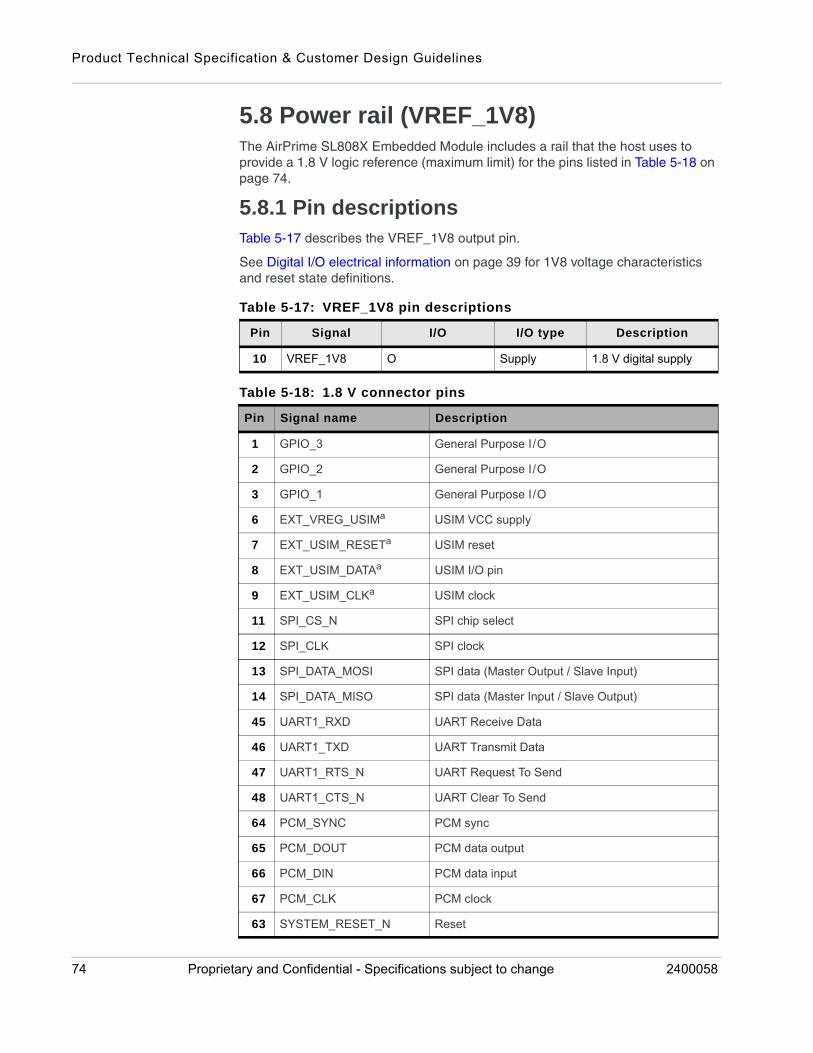
Product Technical Specification & Customer Design Guidelines
5.8 Power rail (VREF_1V8)The AirPrime SL808X Embedded Module includes a rail that the host uses to provide a 1.8 V logic reference (maximum limit) for the pins listed in Table 5-18 on page 74.
5.8.1 Pin descriptionsTable 5-17 describes the VREF_1V8 output pin.
See Digital I/O electrical information on page 39 for 1V8 voltage characteristics and reset state definitions.
Table 5-17: VREF_1V8 pin descriptions
Pin Signal I/O I/O type Description
10 VREF_1V8 O Supply 1.8 V digital supply
Table 5-18: 1.8 V connector pins
Pin Signal name Description
1 GPIO_3 General Purpose I/O
2 GPIO_2 General Purpose I/O
3 GPIO_1 General Purpose I/O
6 EXT_VREG_USIMa USIM VCC supply
7 EXT_USIM_RESETa USIM reset
8 EXT_USIM_DATAa USIM I/O pin
9 EXT_USIM_CLKa USIM clock
11 SPI_CS_N SPI chip select
12 SPI_CLK SPI clock
13 SPI_DATA_MOSI SPI data (Master Output / Slave Input)
14 SPI_DATA_MISO SPI data (Master Input / Slave Output)
45 UART1_RXD UART Receive Data
46 UART1_TXD UART Transmit Data
47 UART1_RTS_N UART Request To Send
48 UART1_CTS_N UART Clear To Send
64 PCM_SYNC PCM sync
65 PCM_DOUT PCM data output
66 PCM_DIN PCM data input
67 PCM_CLK PCM clock
63 SYSTEM_RESET_N Reset
74 Proprietary and Confidential - Specifications subject to change 2400058
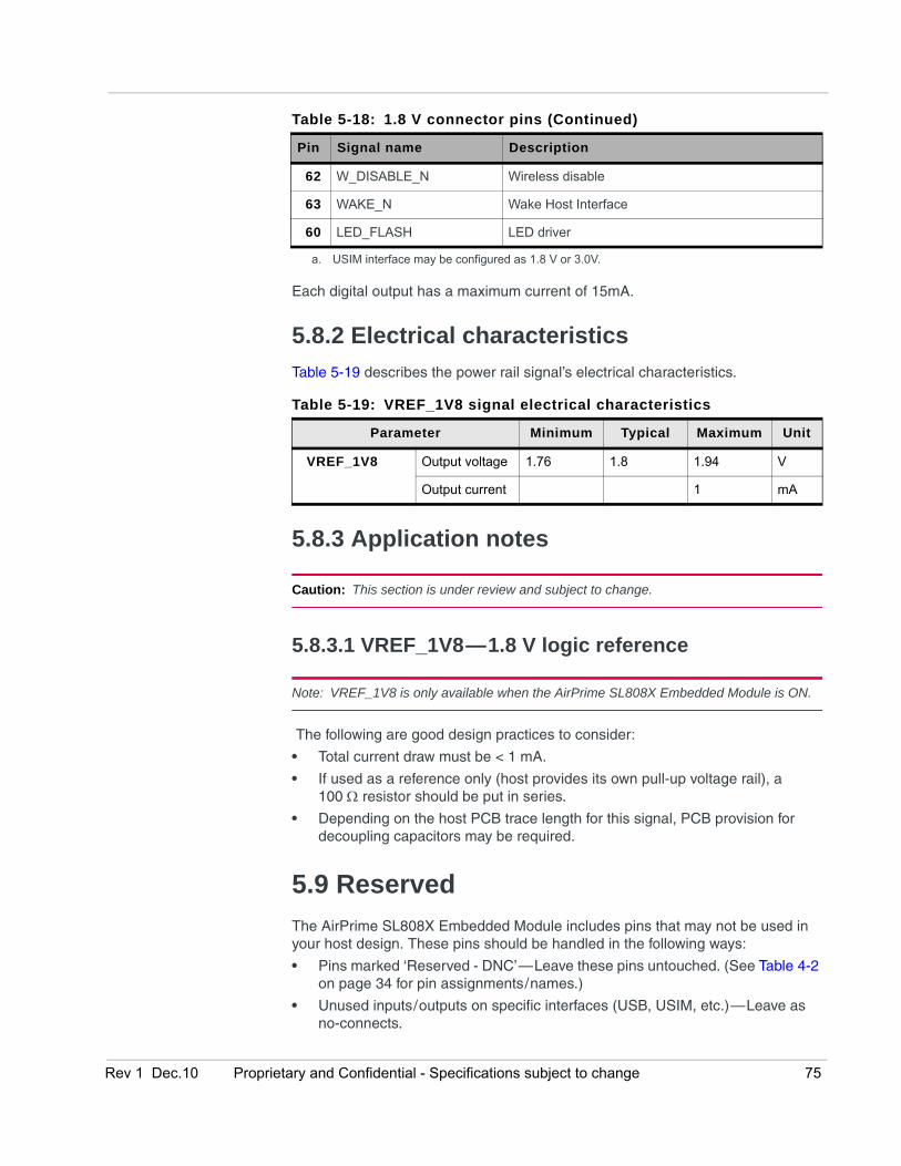
Each digital output has a maximum current of 15mA.
5.8.2 Electrical characteristics
Table 5-19 describes the power rail signal’s electrical characteristics.
5.8.3 Application notes
Caution: This section is under review and subject to change.
5.8.3.1 VREF_1V8—1.8 V logic reference
Note: VREF_1V8 is only available when the AirPrime SL808X Embedded Module is ON.
The following are good design practices to consider:
• Total current draw must be < 1 mA.
• If used as a reference only (host provides its own pull-up voltage rail), a 100 resistor should be put in series.
• Depending on the host PCB trace length for this signal, PCB provision for decoupling capacitors may be required.
5.9 Reserved
The AirPrime SL808X Embedded Module includes pins that may not be used in your host design. These pins should be handled in the following ways:
• Pins marked ‘Reserved - DNC’—Leave these pins untouched. (See Table 4-2 on page 34 for pin assignments/names.)
• Unused inputs/outputs on specific interfaces (USB, USIM, etc.)—Leave as no-connects.
62 W_DISABLE_N Wireless disable
63 WAKE_N Wake Host Interface
60 LED_FLASH LED driver
a. USIM interface may be configured as 1.8 V or 3.0V.
Table 5-19: VREF_1V8 signal electrical characteristics
Parameter Minimum Typical Maximum Unit
VREF_1V8 Output voltage 1.76 1.8 1.94 V
Output current 1 mA
Table 5-18: 1.8 V connector pins (Continued)
Pin Signal name Description
Rev 1 Dec.10 Proprietary and Confidential - Specifications subject to change 75

Product Technical Specification & Customer Design Guidelines
76 Proprietary and Confidential - Specifications subject to change 2400058
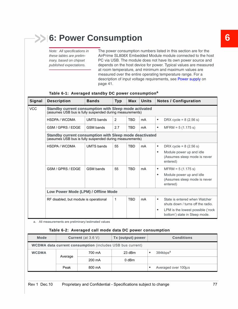
Rev 1 Dec
6
Signal
VCC
a. All m
Mode
WCDMA
WCDMA
6: Power ConsumptionNote: All specifications in these tables are prelim-inary, based on chipset published expectations.
The power consumption numbers listed in this section are for the AirPrime SL808X Embedded Module module connected to the host PC via USB. The module does not have its own power source and depends on the host device for power. Typical values are measured at room temperature, and minimum and maximum values are measured over the entire operating temperature range. For a description of input voltage requirements, see Power supply on page 41.
Table 6-1: Averaged standby DC power consumptiona
Description Bands Typ Max Units Notes / Configuration
Standby current consumption with Sleep mode activated(assumes USB bus is fully suspended during measurements)
HSDPA / WCDMA UMTS bands 2 TBD mA • DRX cycle = 8 (2.56 s)
GSM / GPRS / EDGE GSM bands 2.7 TBD mA • MFRM = 5 (1.175 s)
Standby current consumption with Sleep mode deactivated(assumes USB bus is fully suspended during measurements)
HSDPA / WCDMA UMTS bands 55 TBD mA • DRX cycle = 8 (2.56 s)
• Module power up and idle (Assumes sleep mode is never entered)
GSM / GPRS / EDGE GSM bands 55 TBD mA • MFRM = 5 (1.175 s)
• Module power up and idle (Assumes sleep mode is never entered)
Low Power Mode (LPM) / Offline Mode
RF disabled, but module is operational 1 TBD mA • State is entered when Watcher shuts down / turns off the radio.
• LPM is the lowest possible (‘rock bottom’) state in Sleep mode.
easurements are preliminary/estimated values
Table 6-2: Averaged call mode data DC power consumption
Current (at 3.6 V) Tx (output) power Conditions
data current consumption (includes USB bus current)
Average700 mA 23 dBm • 384kbpsa
200 mA 0 dBm
Peak 800 mA • Averaged over 100s
.10 Proprietary and Confidential - Specifications subject to change 77
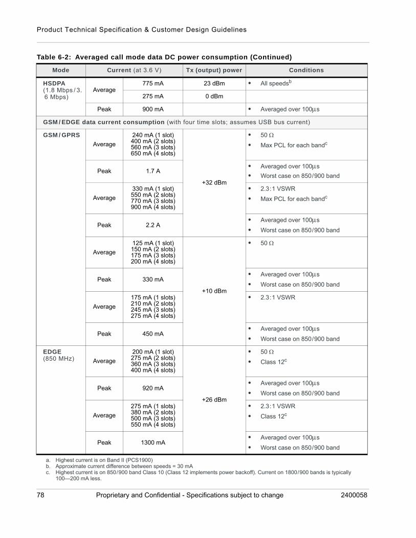
Product Technical Specification & Customer Design Guidelines
HSDPA(1.8 Mbps / 3.6 Mbps)
Average775 mA 23 dBm • All speedsb
275 mA 0 dBm
Peak 900 mA • Averaged over 100s
GSM / EDGE data current consumption (with four time slots; assumes USB bus current)
GSM / GPRS
Average
240 mA (1 slot)400 mA (2 slots)560 mA (3 slots)650 mA (4 slots)
+32 dBm
• 50
• Max PCL for each bandc
Peak 1.7 A• Averaged over 100s
• Worst case on 850/900 band
Average
330 mA (1 slot)550 mA (2 slots)770 mA (3 slots)900 mA (4 slots)
• 2.3:1 VSWR
• Max PCL for each bandc
Peak 2.2 A• Averaged over 100s
• Worst case on 850/900 band
Average
125 mA (1 slot)150 mA (2 slots)175 mA (3 slots)200 mA (4 slots)
+10 dBm
• 50
Peak 330 mA• Averaged over 100s
• Worst case on 850/900 band
Average
175 mA (1 slots)210 mA (2 slots)245 mA (3 slots)275 mA (4 slots)
• 2.3:1 VSWR
Peak 450 mA• Averaged over 100s
• Worst case on 850/900 band
EDGE(850 MHz) Average
200 mA (1 slot)275 mA (2 slots)360 mA (3 slots)400 mA (4 slots)
+26 dBm
• 50
• Class 12c
Peak 920 mA• Averaged over 100s
• Worst case on 850/900 band
Average
275 mA (1 slots)380 mA (2 slots)500 mA (3 slots)550 mA (4 slots)
• 2.3:1 VSWR
• Class 12c
Peak 1300 mA• Averaged over 100s
• Worst case on 850/900 band
a. Highest current is on Band II (PCS1900)b. Approximate current difference between speeds = 30 mAc. Highest current is on 850/900 band Class 10 (Class 12 implements power backoff). Current on 1800/900 bands is typically
100—200 mA less.
Table 6-2: Averaged call mode data DC power consumption (Continued)
Mode Current (at 3.6 V) Tx (output) power Conditions
78 Proprietary and Confidential - Specifications subject to change 2400058
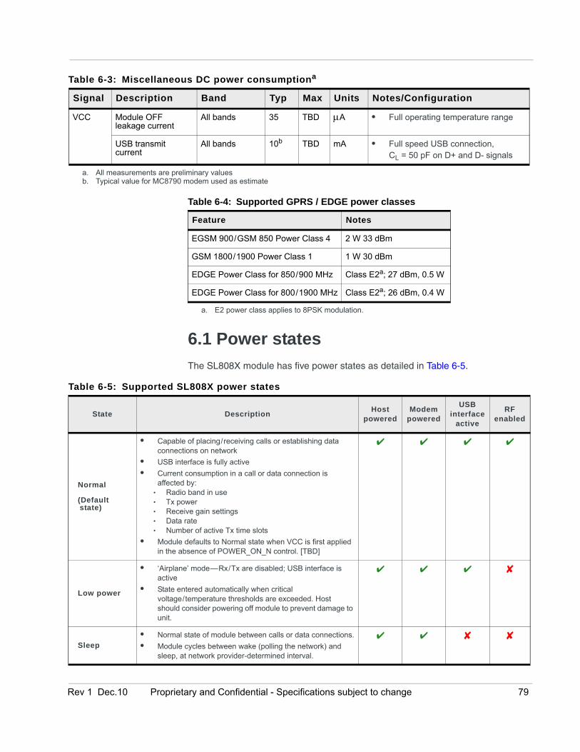
6.1 Power states
The SL808X module has five power states as detailed in Table 6-5.
Table 6-3: Miscellaneous DC power consumptiona
Signal Description Band Typ Max Units Notes/Configuration
VCC Module OFF leakage current
All bands 35 TBD A • Full operating temperature range
USB transmit current
All bands 10b TBD mA • Full speed USB connection,CL = 50 pF on D+ and D- signals
a. All measurements are preliminary valuesb. Typical value for MC8790 modem used as estimate
Table 6-4: Supported GPRS / EDGE power classes
Feature Notes
EGSM 900/GSM 850 Power Class 4 2 W 33 dBm
GSM 1800/1900 Power Class 1 1 W 30 dBm
EDGE Power Class for 850/900 MHz Class E2a; 27 dBm, 0.5 W
EDGE Power Class for 800/1900 MHz Class E2a; 26 dBm, 0.4 W
a. E2 power class applies to 8PSK modulation.
Table 6-5: Supported SL808X power states
State DescriptionHost
poweredModem
powered
USB interface
active
RF enabled
Normal
(Default state)
• Capable of placing/receiving calls or establishing data connections on network
• USB interface is fully active
• Current consumption in a call or data connection is affected by:
· Radio band in use· Tx power· Receive gain settings· Data rate· Number of active Tx time slots
• Module defaults to Normal state when VCC is first applied in the absence of POWER_ON_N control. [TBD]
Low power
• ‘Airplane’ mode—Rx/Tx are disabled; USB interface is active
• State entered automatically when critical voltage/temperature thresholds are exceeded. Host should consider powering off module to prevent damage to unit.
Sleep• Normal state of module between calls or data connections.
• Module cycles between wake (polling the network) and sleep, at network provider-determined interval.
Rev 1 Dec.10 Proprietary and Confidential - Specifications subject to change 79
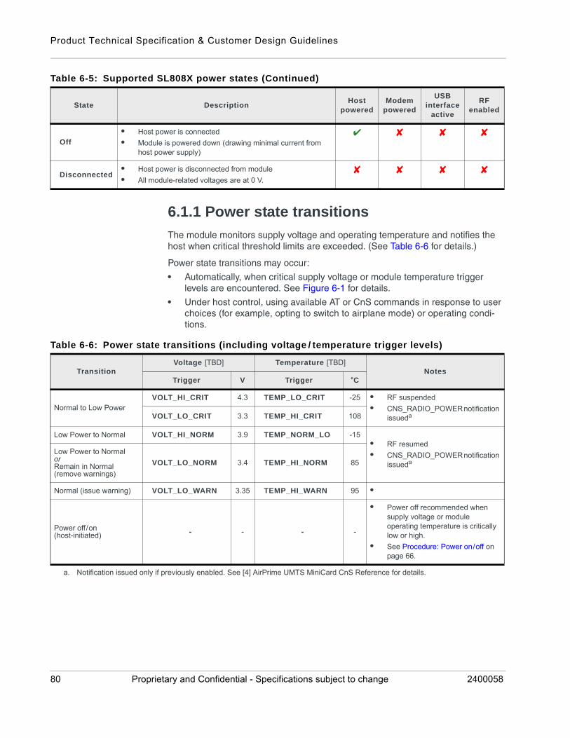
Product Technical Specification & Customer Design Guidelines
6.1.1 Power state transitions
The module monitors supply voltage and operating temperature and notifies the host when critical threshold limits are exceeded. (See Table 6-6 for details.)
Power state transitions may occur:
• Automatically, when critical supply voltage or module temperature trigger levels are encountered. See Figure 6-1 for details.
• Under host control, using available AT or CnS commands in response to user choices (for example, opting to switch to airplane mode) or operating condi-tions.
Off• Host power is connected
• Module is powered down (drawing minimal current from host power supply)
Disconnected• Host power is disconnected from module
• All module-related voltages are at 0 V.
Table 6-5: Supported SL808X power states (Continued)
State DescriptionHost
poweredModem
powered
USB interface
active
RF enabled
Table 6-6: Power state transitions (including voltage / temperature trigger levels)
TransitionVoltage [TBD] Temperature [TBD]
Notes Trigger V Trigger °C
Normal to Low PowerVOLT_HI_CRIT 4.3 TEMP_LO_CRIT -25 • RF suspended
• CNS_RADIO_POWER notification issuedaVOLT_LO_CRIT 3.3 TEMP_HI_CRIT 108
Low Power to Normal VOLT_HI_NORM 3.9 TEMP_NORM_LO -15• RF resumed
• CNS_RADIO_POWER notification issueda
Low Power to NormalorRemain in Normal (remove warnings)
VOLT_LO_NORM 3.4 TEMP_HI_NORM 85
Normal (issue warning) VOLT_LO_WARN 3.35 TEMP_HI_WARN 95 •
Power off/on(host-initiated) - - - -
• Power off recommended when supply voltage or module operating temperature is critically low or high.
• See Procedure: Power on/off on page 66.
a. Notification issued only if previously enabled. See [4] AirPrime UMTS MiniCard CnS Reference for details.
80 Proprietary and Confidential - Specifications subject to change 2400058
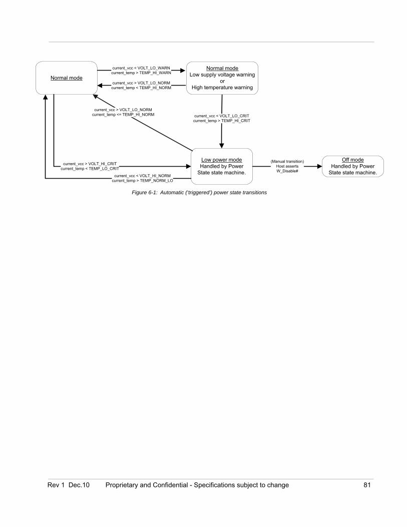
Figure 6-1: Automatic (‘triggered’) power state transitions
Off modeHandled by Power
State state machine.
Normal mode
Low power modeHandled by Power
State state machine.
current_vcc > VOLT_LO_NORMcurrent_temp <= TEMP_HI_NORM current_vcc < VOLT_LO_CRIT
current_temp > TEMP_HI_CRIT
current_vcc > VOLT_LO_NORMcurrent_temp < TEMP_HI_NORM
current_vcc < VOLT_LO_WARNcurrent_temp > TEMP_HI_WARN
current_vcc < VOLT_HI_NORMcurrent_temp > TEMP_NORM_LO
current_vcc > VOLT_HI_CRITcurrent_temp < TEMP_LO_CRIT
(Manual transition)Host assertsW_Disable#
Normal modeLow supply voltage warning
orHigh temperature warning
Rev 1 Dec.10 Proprietary and Confidential - Specifications subject to change 81

Product Technical Specification & Customer Design Guidelines
82 Proprietary and Confidential - Specifications subject to change 2400058
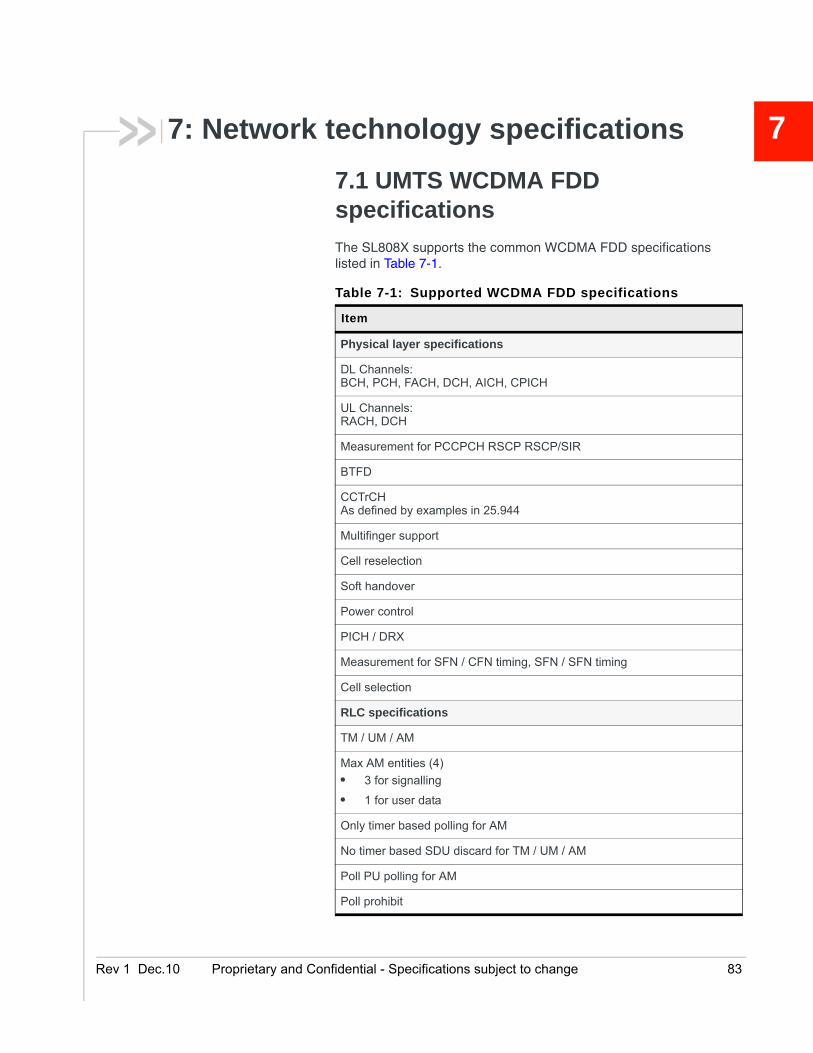
Rev 1 Dec
7
7: Network technology specifications7.1 UMTS WCDMA FDD specifications
The SL808X supports the common WCDMA FDD specifications listed in Table 7-1.
Table 7-1: Supported WCDMA FDD specifications
Item
Physical layer specifications
DL Channels:BCH, PCH, FACH, DCH, AICH, CPICH
UL Channels:RACH, DCH
Measurement for PCCPCH RSCP RSCP/SIR
BTFD
CCTrCHAs defined by examples in 25.944
Multifinger support
Cell reselection
Soft handover
Power control
PICH / DRX
Measurement for SFN / CFN timing, SFN / SFN timing
Cell selection
RLC specifications
TM / UM / AM
Max AM entities (4)
• 3 for signalling
• 1 for user data
Only timer based polling for AM
No timer based SDU discard for TM / UM / AM
Poll PU polling for AM
Poll prohibit
.10 Proprietary and Confidential - Specifications subject to change 83
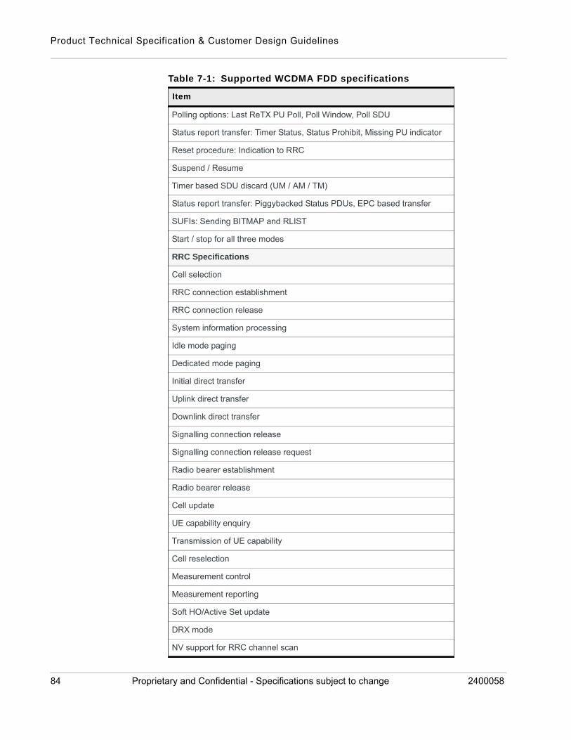
Product Technical Specification & Customer Design Guidelines
Polling options: Last ReTX PU Poll, Poll Window, Poll SDU
Status report transfer: Timer Status, Status Prohibit, Missing PU indicator
Reset procedure: Indication to RRC
Suspend / Resume
Timer based SDU discard (UM / AM / TM)
Status report transfer: Piggybacked Status PDUs, EPC based transfer
SUFIs: Sending BITMAP and RLIST
Start / stop for all three modes
RRC Specifications
Cell selection
RRC connection establishment
RRC connection release
System information processing
Idle mode paging
Dedicated mode paging
Initial direct transfer
Uplink direct transfer
Downlink direct transfer
Signalling connection release
Signalling connection release request
Radio bearer establishment
Radio bearer release
Cell update
UE capability enquiry
Transmission of UE capability
Cell reselection
Measurement control
Measurement reporting
Soft HO/Active Set update
DRX mode
NV support for RRC channel scan
Table 7-1: Supported WCDMA FDD specifications
Item
84 Proprietary and Confidential - Specifications subject to change 2400058
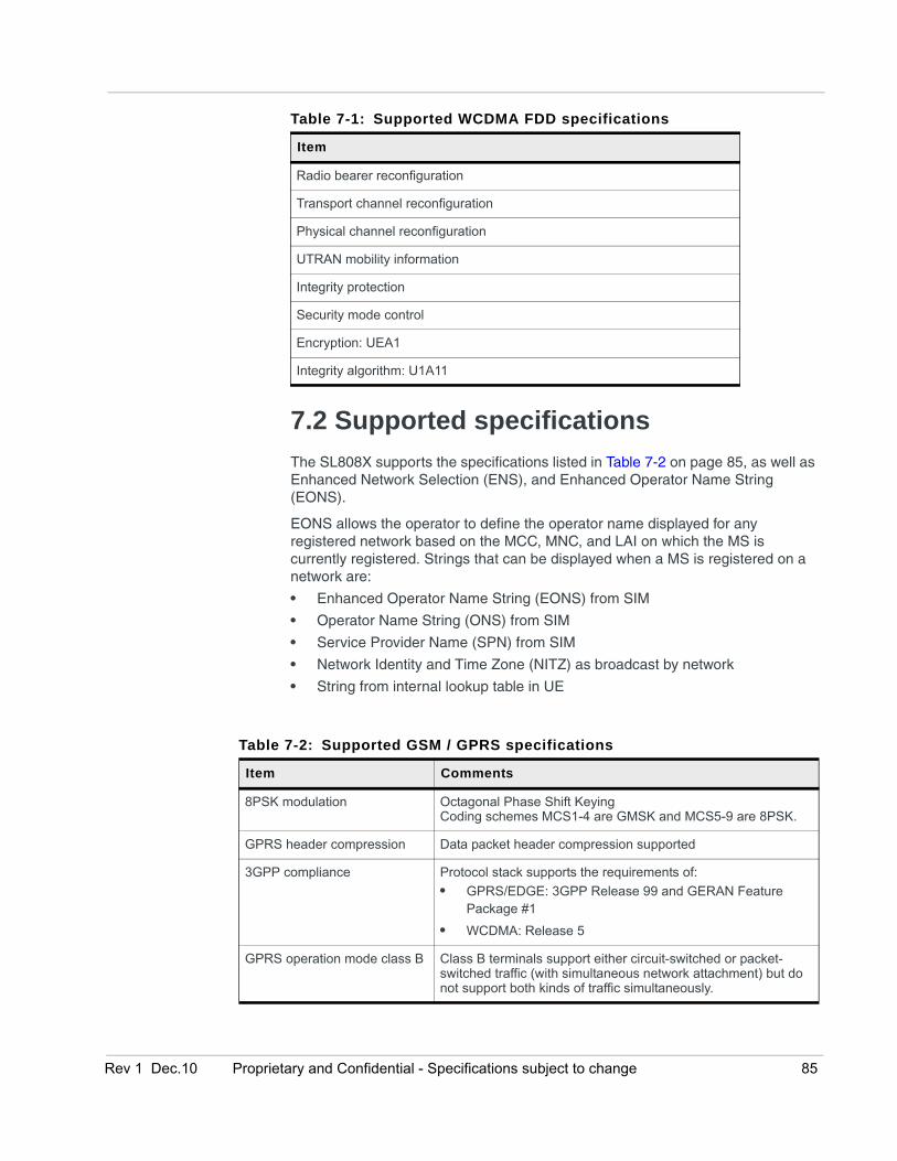
7.2 Supported specifications
The SL808X supports the specifications listed in Table 7-2 on page 85, as well as Enhanced Network Selection (ENS), and Enhanced Operator Name String (EONS).
EONS allows the operator to define the operator name displayed for any registered network based on the MCC, MNC, and LAI on which the MS is currently registered. Strings that can be displayed when a MS is registered on a network are:
• Enhanced Operator Name String (EONS) from SIM
• Operator Name String (ONS) from SIM
• Service Provider Name (SPN) from SIM
• Network Identity and Time Zone (NITZ) as broadcast by network
• String from internal lookup table in UE
Radio bearer reconfiguration
Transport channel reconfiguration
Physical channel reconfiguration
UTRAN mobility information
Integrity protection
Security mode control
Encryption: UEA1
Integrity algorithm: U1A11
Table 7-1: Supported WCDMA FDD specifications
Item
Table 7-2: Supported GSM / GPRS specifications
Item Comments
8PSK modulation Octagonal Phase Shift KeyingCoding schemes MCS1-4 are GMSK and MCS5-9 are 8PSK.
GPRS header compression Data packet header compression supported
3GPP compliance Protocol stack supports the requirements of:
• GPRS/EDGE: 3GPP Release 99 and GERAN Feature Package #1
• WCDMA: Release 5
GPRS operation mode class B Class B terminals support either circuit-switched or packet-switched traffic (with simultaneous network attachment) but do not support both kinds of traffic simultaneously.
Rev 1 Dec.10 Proprietary and Confidential - Specifications subject to change 85
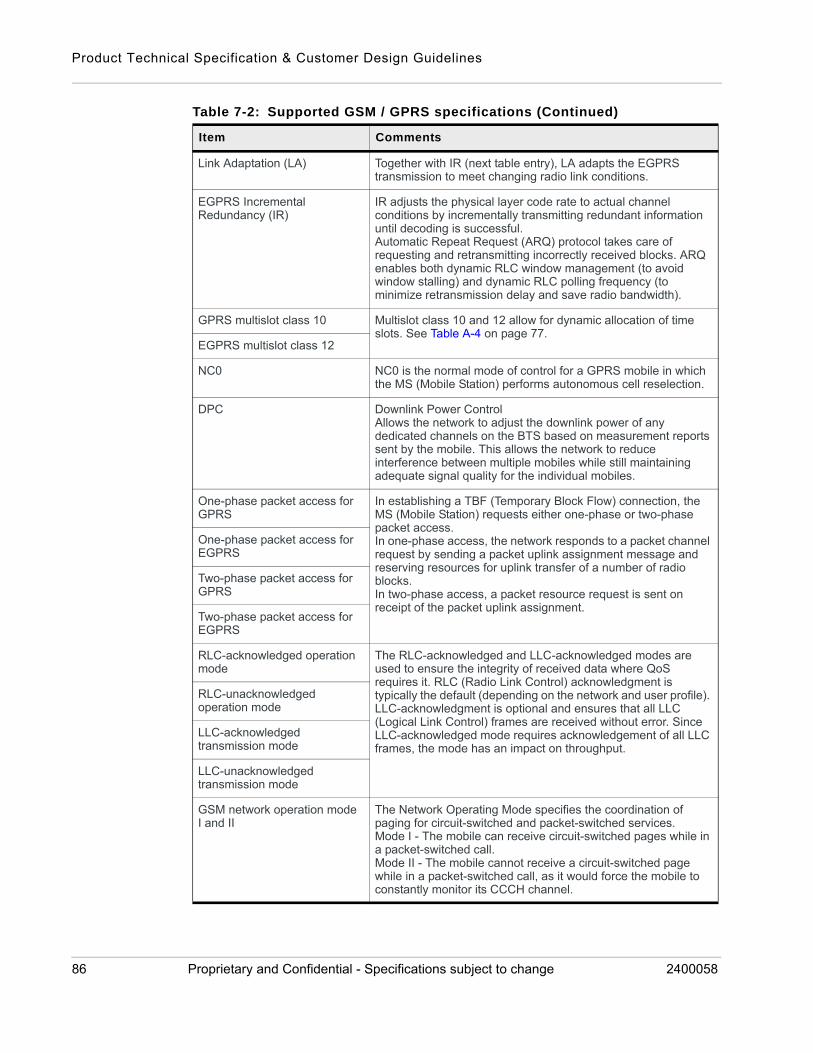
Product Technical Specification & Customer Design Guidelines
Link Adaptation (LA) Together with IR (next table entry), LA adapts the EGPRS transmission to meet changing radio link conditions.
EGPRS Incremental Redundancy (IR)
IR adjusts the physical layer code rate to actual channel conditions by incrementally transmitting redundant information until decoding is successful.Automatic Repeat Request (ARQ) protocol takes care of requesting and retransmitting incorrectly received blocks. ARQ enables both dynamic RLC window management (to avoid window stalling) and dynamic RLC polling frequency (to minimize retransmission delay and save radio bandwidth).
GPRS multislot class 10 Multislot class 10 and 12 allow for dynamic allocation of time slots. See Table A-4 on page 77.
EGPRS multislot class 12
NC0 NC0 is the normal mode of control for a GPRS mobile in which the MS (Mobile Station) performs autonomous cell reselection.
DPC Downlink Power ControlAllows the network to adjust the downlink power of any dedicated channels on the BTS based on measurement reports sent by the mobile. This allows the network to reduce interference between multiple mobiles while still maintaining adequate signal quality for the individual mobiles.
One-phase packet access for GPRS
In establishing a TBF (Temporary Block Flow) connection, the MS (Mobile Station) requests either one-phase or two-phase packet access.In one-phase access, the network responds to a packet channel request by sending a packet uplink assignment message and reserving resources for uplink transfer of a number of radio blocks.In two-phase access, a packet resource request is sent on receipt of the packet uplink assignment.
One-phase packet access for EGPRS
Two-phase packet access for GPRS
Two-phase packet access for EGPRS
RLC-acknowledged operation mode
The RLC-acknowledged and LLC-acknowledged modes are used to ensure the integrity of received data where QoS requires it. RLC (Radio Link Control) acknowledgment is typically the default (depending on the network and user profile). LLC-acknowledgment is optional and ensures that all LLC (Logical Link Control) frames are received without error. Since LLC-acknowledged mode requires acknowledgement of all LLC frames, the mode has an impact on throughput.
RLC-unacknowledged operation mode
LLC-acknowledged transmission mode
LLC-unacknowledged transmission mode
GSM network operation mode I and II
The Network Operating Mode specifies the coordination of paging for circuit-switched and packet-switched services.Mode I - The mobile can receive circuit-switched pages while in a packet-switched call.Mode II - The mobile cannot receive a circuit-switched page while in a packet-switched call, as it would force the mobile to constantly monitor its CCCH channel.
Table 7-2: Supported GSM / GPRS specifications (Continued)
Item Comments
86 Proprietary and Confidential - Specifications subject to change 2400058
(SL8080/82/84)PBCCH / PCCCHI
Packet Broadcast Control ChannelPBCCH is a packet data signaling channel that can supplement the BCCH GSM control channel, allowing decoupling of voice and packet control channels to set up data calls. PBCCH broadcasts GPRS / EGPRS specific cell re-selection parameters for serving and neighbor cells used in cell selection / re-selection for packet services.
GPRS test modes (ETSI test mode A and B)
The European Telecommunications Standards Institute (ETSI) defines standards and requirements for testing of GSM mobile equipment.In test mode A, the mobile requests an uplink TBF and transmits random data on a designated number of timeslots. This causes a device to transmit data without using upper layer protocols. Once the transmission has started, the downlink TBF halts. The device remains in this mode until the testing equipment terminates it.In test mode B, the mobile is prompted to receive data on a number of specified downlink timeslots and re-transmit the same data back on the corresponding uplink timeslots. Test mode B allows tests to be performed on both the transmitter and receiver within a single session.
NACC (R4 GERAN Feature Set 1)
Network Assisted Cell ChangeEnables the network to provide additional information about neighbor cells to the mobile while in a packet data session, which decreases the experienced service delays caused by cell re-selection.
MAIO Mobile Allocation Index OffsetMAIO and Hopping Sequence Number (HSN) are used in conjunction with Frequency Hopping to determine the hopping sequence used in each frame. The MAIO supports as many values as there are frequencies in the hopping list, and these are used to indicate the offset within the hopping list that identifies the frequency used.
Packet enhanced measurement report (PEMR)
Packet Enhanced Measurement Report (PEMR) is one of the RLC / MAC (Radio Link Control and Medium Access Control) control messages that include a carrier identifier. This message is a requirement of supporting multicarrier TBF.
Delayed TBF Release Delayed Temporary Block Flow Release (also called Extended Uplink TBF)Delayed TBF Release reduces latency between uplink data transfers and reduced signaling on the network by maintaining a connection for brief periods when the network is temporarily inactive and the mobile station has no radio link control information to send. For this feature to work properly, the mobile station must support delayed TBF release.
Extended Dynamic Allocation Radio blocks can be transmitted on up to four different PDCHs. Permits full class 12 operation.
Single Antenna Interference Cancellation (SAIC)
SAIC mitigates code-channel interference from neighboring cells resulting in fewer dropped calls, and faster download rates for e-mail and websites.
Table 7-2: Supported GSM / GPRS specifications (Continued)
Item Comments
Rev 1 Dec.10 Proprietary and Confidential - Specifications subject to change 87
Product Technical Specification & Customer Design Guidelines
Circuit-switched data bearers These circuit-switched data bearers are supported on 2G networks:
• Asynchronous 9,600 bps
• Asynchronous 14,400 bps
Security
Encryption support GPRS / EGPRS support GEA1, GEA2, and GEA3 data ciphering.GSM CSD and SMS use A5/1 and A5/3 encryption.
PAP for RADIUS authentication - GPRS / EGPRS
PAP (Password Authentication Protocol) is a method of authenticating usernames and passwords against a database on a RADIUS (Remote Authentication Dial-In User Service) server. In a standard login, the service provider prompts for a username and password. In PAP authentication, the username and password are entered in the client's dialing software and sent as one data package, rather than the server sending a login prompt and waiting for a response.
CHAP for RADIUS authentication - GPRS / EGPRS
CHAP (Challenge Handshake Authentication Protocol) is a more secure method for connecting to a system than PAP. After a link is established, the server sends a challenge message to the client. The client responds with a value calculated using a one-way hash function. The server compares its own calculation of the expected hash value to the client's response. If the values match, the authentication is acknowledged; otherwise the connection is terminated.
Support for encryption algorithm UEA1 (Kasumi)
UEA1 (UMTS Encryption Algorithm) generates the keystream as a function of a cipher key that is re-synchronized to every MAC / RLC frame. UEA is based on the Kasumi algorithm.
Support for integrity algorithm UIA1 (Kasumi)
UIA1 (UMTS Integrity Algorithm) is the algorithm used to compute the IK (Integrity Key) used in message authentication. UIA is based on the Kasumi algorithm.
UMTS
WCDMA-to-GPRS reselection in CELL_FACH
CELL_FACH is an RRC (Radio Resource Control) service state in which cell reselection is performed. This feature prevents dropping of RRC connections.
Inter-frequency reselection in Cell_FACH
Radio link failure Radio link failure is a procedure that indicates an ‘out-of-synch’ state on one or more radio links. Node B of the RNC (Radio Network Controller) reports this event before attempting resynchronization. The radio link restoration procedure indicates restoration of the ‘synchronized’ state.
SIB scheduling SIB (System Information Block) scheduling controls the broadcasting of information to user equipment in a cell. The user equipment retrieves the schedule, and is then able to change to sleep mode, receiving only those blocks that it needs.
SIB modification
Re-establishment procedure Following a radio link failure, the RNC maintains the RRC connection, waiting for re-establishment.
Table 7-2: Supported GSM / GPRS specifications (Continued)
Item Comments
88 Proprietary and Confidential - Specifications subject to change 2400058
VT + PS call (subject to network availability)
Simultaneous VT (Video Terminal) and PS (Packet Switched) calls are supported.
Packet Cell Change Order from GSMUTRAN
Call transfer between GSM-based and UTRAN-based cells is supported.
Background PLMN search Improved algorithm for Higher Priority PLMN (HPPLMN) search while camped on a 3G cell.
Configurable Release 5 or Release 99 support
Circuit-switched data bearers
Data bearers These circuit-switched data bearers are supported on 3G networks:
• Synchronous transparent mode = 64000 bps
• Synchronous transparent mode = 56000 bps
• Asynchronous V110 UDI = 14400 bps
• Asynchronous V110 UDI = 28800 bps
• Asynchronous V110 UDI = 38400 bps
• Asynchronous V120 = 14400 bps
• Asynchronous V120 = 28800 bps
• Asynchronous V120 = 56000 bps
HSDPA
Data rates The following data rates are supported:
• Category 12 (1.8 Mbps)
• Category 5/6 (3.6 Mbps)
HSDPA logical channels These HSDPA logical channels are supported:
• HS-SCCH
• HS-DPCCH
• HS-PDSCH—Up to ten HS-PDSCH channels are supported.
HSDPA transport channels HS-DSCH is supported at these rates:
• 120 kbps
• 240 kbps
• 360 kbps
Incremental redundancy IR adjusts the physical layer code rate to actual channel conditions by incrementally transmitting redundant information until decoding is successful. Automatic Repeat Request (ARQ) protocol takes care of requesting and retransmitting incorrectly received blocks. ARQ enables both dynamic RLC window management (to avoid window stalling) and dynamic RLC polling frequency (to minimize retransmission delay and save radio bandwidth).
Table 7-2: Supported GSM / GPRS specifications (Continued)
Item Comments
Rev 1 Dec.10 Proprietary and Confidential - Specifications subject to change 89

Product Technical Specification & Customer Design Guidelines
Chase combining retransmission scheme
The Chase combining retransmission scheme is the simplest HARQ (Hybrid Automatic Request) link adaptation technique. HARQ techniques are used to enhance system performance.
HSDPA Compressed Mode Allows the user equipment to interrupt transmission and reception during a call for brief periods in order to measure the signal strength of neighboring cells that use different frequencies.
(SL8080/82/84)Concurrent voice and HSDPA data
HSDPA Indicator Allows user interface to display an indicator when HSDPA data transfer is in progress.
Receiver equalizer support
Miscellaneous
Fast link adaptation The data rate is adapted to radio conditions.
Vary the effective code rate The effective code rate is varied based on code space resources.
HARQ, MAC-HS disassembly MAC-HS (High Speed MAC) is the base station MAC (Medium Access Control) protocol. MAC-HS enables fast radio resource allocation.MAC-HS reordering queue
distribution and processing support
Cell change These cell change methods are supported:
• Synchronous and non-synchronous
• Intra-Node B (softer repointing)
• Inter-Node B (soft repointing)
Up-switching and down-switching of PS RAB between HS-PDSCH and DPCH
RAB (Radio Access Bearer) and channel mappings between the HS-PDSCH (High Speed Physical Downlink Shared Channel) and DPCH (Dedicated Physical Channel) are reallocated according to volume thresholds and inactivity timers.
Ciphering on the HS channel Ciphering on high-speed channels protects radio-transmitted data against unauthorized third parties.
Support to not resume the HS channel if inter-RAT handover fails, but save the RB mapping information
RB (Radio Bearer) mapping information is preserved if a high-speed channel is dropped due to the failure of an inter-RAT (Radio Access Technology) transfer.
Support to not resume the HS channel if a radio link failure occurs, but save the RB mapping information
RB (Radio Bearer) mapping information is preserved if a high-speed channel is dropped due to a radio link failure.
WINS address support primary and secondary
Primary and secondary IP addresses can be assigned for WINS (Windows Internet Name Service) name servers.
(SL8080/82/84)Voice support
Table 7-2: Supported GSM / GPRS specifications (Continued)
Item Comments
90 Proprietary and Confidential - Specifications subject to change 2400058
7.3 UMTS (WCDMA) / GSM specificationsTable 7-3 details the SL808X modem’s support for common UMTS (WCDMA) and GSM specifications.
Unstructured supplementary services data (USSD)
USSD provides support for transmitting information over the GSM network signalling channels. It provides fast session-based communication between the user and an application, enabling use of text messaging, prepaid roaming, chat, etc.
(SL8080/82/84)Supplementary services
Support for supplementary voice services such as Call Hold, Call Forward, Call Waiting, Multi-party Calls, Caller ID, Fixed Number Dialing, Service Dialing Numbers, etc.
Cell reselection/handover Supports InterRat and InterFrequency cell-reselection and handover between supported frequency bands.
Security - IMEI Security
SIM lock The device can be ‘MEP locked’ to a particular PLMN.
SIM security Both CHV1 and CHV2 are supported (unlock and unblock).
Table 7-2: Supported GSM / GPRS specifications (Continued)
Item Comments
Table 7-3: UMTS (WCDMA) / GSM specificationsa
Item GSM UMTS
Mobility management
Automatic PLMN selection / reselection
Location updating procedure
IMSI attach procedure
IMSI detach procedure
Periodic location update
Authentication procedure
CM connection establishment from MS or network
CM connection release
Encryption key management
TMSI reallocation
Paging response
Abort procedure
Identification
CN system information
Call re-establishment
Rev 1 Dec.10 Proprietary and Confidential - Specifications subject to change 91

Product Technical Specification & Customer Design Guidelines
MM connection establishment emergency calls
Inter-RAT change procedure
CS follow-on procedure
Access class barring
Resumption procedure for Class B operation in GPRS
Handling of domain change CS to CS/PS and other combinations
MM information
Network mode of operation I, II
GPRS mobility management
GPRS attach
GPRS detach
Routing area update
GPRS authentication
GPRS identification
GMM status
Periodic routing area update
Ciphering
Access class barring
GMM status
Combined GPRS attach
Combined GPRS detach
Combined routing location / area update
PS SMS
Network initiated combined GPRS detach
Network mode of operation change
RAB management
QoS-based activation, network offers lower / higher QoS
Primary PDP context activation
PDP context deactivation
Data services
AT commands
Table 7-3: UMTS (WCDMA) / GSM specificationsa (Continued)
Item GSM UMTS
92 Proprietary and Confidential - Specifications subject to change 2400058
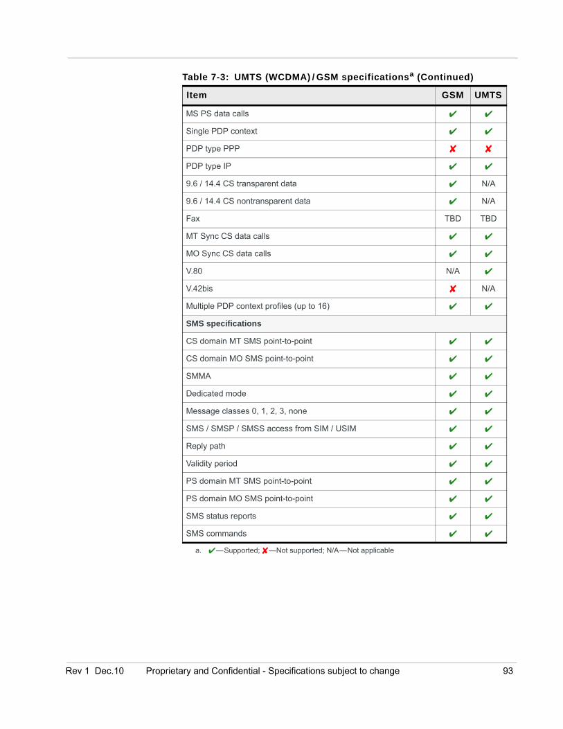
MS PS data calls
Single PDP context
PDP type PPP
PDP type IP
9.6 / 14.4 CS transparent data N/A
9.6 / 14.4 CS nontransparent data N/A
Fax TBD TBD
MT Sync CS data calls
MO Sync CS data calls
V.80 N/A
V.42bis N/A
Multiple PDP context profiles (up to 16)
SMS specifications
CS domain MT SMS point-to-point
CS domain MO SMS point-to-point
SMMA
Dedicated mode
Message classes 0, 1, 2, 3, none
SMS / SMSP / SMSS access from SIM / USIM
Reply path
Validity period
PS domain MT SMS point-to-point
PS domain MO SMS point-to-point
SMS status reports
SMS commands
a. —Supported; —Not supported; N/A—Not applicable
Table 7-3: UMTS (WCDMA) / GSM specificationsa (Continued)
Item GSM UMTS
Rev 1 Dec.10 Proprietary and Confidential - Specifications subject to change 93

Product Technical Specification & Customer Design Guidelines
94 Proprietary and Confidential - Specifications subject to change 2400058
Rev 1 Dec
8
8: Design GuidelinesThis chapter provides general design guidelines for the AirPrime SL808X Embedded Module.Caution: This chapter is under development—all recommendations must be considered as ‘TBD’.
For industrial assembly guidelines, refer to [7] Customer Process Guidelines—AirPrime SL Series, available from your Sierra Wireless account representative.
8.1 General rules and constraints
Clock and other high frequency digital signals (e.g. serial buses) should be routed as far as possible from the AirPrime SL808X Embedded Module analog signals.
If the application design makes it possible, all analog signals should be separated from digital signals by a ground line on the PCB.
Tip: It is recommended to avoid routing any signals under the AirPrime SL808X Embedded Module on the application board.
8.2 PCB layout recommendations
Ground slugs should be reflowed on to the host PCB with <25% voiding to allow effective heat dissipation.
8.3 Power supply
The power supply is one of the key issues in the design of a GSM terminal.
A weak power supply design could, in particular, affect:
• EMC performance
• The emission spectrum
• The phase error and frequency error
When designing the power supply, careful attention should be paid to the following:
• The quality of the power supply—low ripple, PFM or PSM systems should be avoided; linear regulation or PWM converters are preferred for low noise.
.10 Proprietary and Confidential - Specifications subject to change 95
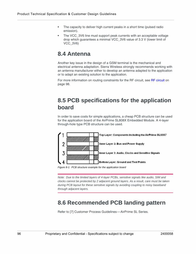
Product Technical Specification & Customer Design Guidelines
• The capacity to deliver high current peaks in a short time (pulsed radio emission).
• The VCC_3V6 line must support peak currents with an acceptable voltage drop which guarantees a minimal VCC_3V6 value of 3.3 V (lower limit of VCC_3V6)
8.4 Antenna
Another key issue in the design of a GSM terminal is the mechanical and electrical antenna adaptation. Sierra Wireless strongly recommends working with an antenna manufacturer either to develop an antenna adapted to the application or to adapt an existing solution to the application.
For more information on routing constraints for the RF circuit, see RF circuit on page 98.
8.5 PCB specifications for the application board
In order to save costs for simple applications, a cheap PCB structure can be used for the application board of the AirPrime SL808X Embedded Module. A 4-layer through-hole type PCB structure can be used.
Figure 8-1: PCB structure example for the application board
Note: Due to the limited layers of 4-layer PCBs, sensitive signals like audio, SIM and clocks cannot be protected by 2 adjacent ground layers. As a result, care must be taken during PCB layout for these sensitive signals by avoiding coupling to noisy baseband through adjacent layers.
8.6 Recommended PCB landing pattern
Refer to [7] Customer Process Guidelines—AirPrime SL Series.
96 Proprietary and Confidential - Specifications subject to change 2400058
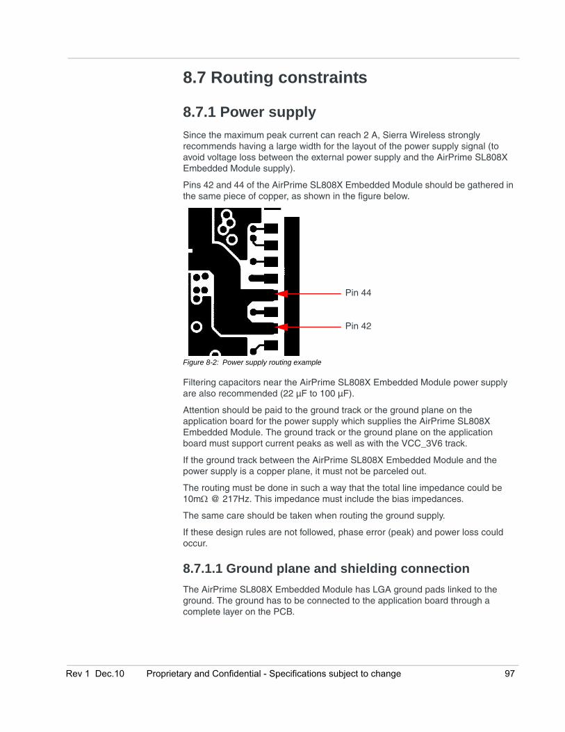
8.7 Routing constraints
8.7.1 Power supply
Since the maximum peak current can reach 2 A, Sierra Wireless strongly recommends having a large width for the layout of the power supply signal (to avoid voltage loss between the external power supply and the AirPrime SL808X Embedded Module supply).
Pins 42 and 44 of the AirPrime SL808X Embedded Module should be gathered in the same piece of copper, as shown in the figure below.
Figure 8-2: Power supply routing example
Filtering capacitors near the AirPrime SL808X Embedded Module power supply are also recommended (22 µF to 100 µF).
Attention should be paid to the ground track or the ground plane on the application board for the power supply which supplies the AirPrime SL808X Embedded Module. The ground track or the ground plane on the application board must support current peaks as well as with the VCC_3V6 track.
If the ground track between the AirPrime SL808X Embedded Module and the power supply is a copper plane, it must not be parceled out.
The routing must be done in such a way that the total line impedance could be 10m @ 217Hz. This impedance must include the bias impedances.
The same care should be taken when routing the ground supply.
If these design rules are not followed, phase error (peak) and power loss could occur.
8.7.1.1 Ground plane and shielding connection
The AirPrime SL808X Embedded Module has LGA ground pads linked to the ground. The ground has to be connected to the application board through a complete layer on the PCB.
Pin 44
Pin 42
Rev 1 Dec.10 Proprietary and Confidential - Specifications subject to change 97

Product Technical Specification & Customer Design Guidelines
A ground plane must be available on the application board to provide efficient connection to the bottom ground of the AirPrime SL808X Embedded Module. The bottom side shielding of the AirPrime SL808X Embedded Module is achieved by soldering the ground plane of the application board and the AirPrime SL808X Embedded Module.
The best shielding performance is achieved when the application ground plane is a complete layer of the application PCB. To ensure good shielding of the AirPrime SL808X Embedded Module, a complete ground plane layer on the application board must be available, with no tradeoffs. Connections between other ground planes should be done with bias.
Without this ground plane, external spurious TX or RX blockings could appear.
For more information, see Recommended PCB landing pattern on page 96.
8.7.2 SIM interface
The length of the tracks between the AirPrime SL808X Embedded Module and the SIM socket should be as short as possible. Maximum recommended length is 10cm.
ESD protection is mandatory on the SIM lines if access from outside of the SIM socket is possible.
The capacitor (100 nF) on the EXT_VREG_USIM signal must be placed as close as possible to the DALC208SC6 component on the PCB (see SIM interface on page 42).
8.7.3 Audio circuit
To get better acoustic performances, the basic recommendations are as follows:
• The speaker lines (SPK) must be routed in parallel without any wires in between
• The microphone lines (MIC) must be routed in parallel without any wires in between
All the filtering components (RLC) must be placed as close as possible to the associated MIC and SPK pins.
8.7.4 RF circuit
The RF signal must be routed on the application board using tracks with a 50 characteristic impedance.
Basically, the characteristic impedance depends on the dielectric, the track width and the ground plane spacing.
In order to respect this constraint, Sierra Wireless recommends using MicroStrip or StripLine structure and computing the Tracks width with a simulation tool (like AppCad shown in the figure below and that is available free of charge at http://www.agilent.com).
98 Proprietary and Confidential - Specifications subject to change 2400058

Figure 8-3: AppCad screenshot for MicroStrip design
If a multi-layered PCB is used, the RF path on the board must not cross any signal (digital, analog or supply).
If necessary, use StripLine structure and route the digital line(s) "outside" the RF structure as shown in the figure below.
Figure 8-4: Routing examples
Stripline and Coplanar design requires having a correct ground plane at both sides. Consequently, it is necessary to add some vias along the RF path.
It is recommended to use Stripline design if the RF path is fairly long (more than 3cm), since MicroStrip design is not shielded. Consequently, the RF signal (when transmitting) may interfere with neighboring electronics (AF amplifier, etc.). In the same way, the neighboring electronics (micro-controllers, etc.) may degrade the reception performances.
50 line
LGA pin for ANT
Rev 1 Dec.10 Proprietary and Confidential - Specifications subject to change 99
Product Technical Specification & Customer Design Guidelines
The GSM/GPRS connector is intended to be directly connected to a 50 antenna and no matching is needed.
8.8 EMC and ESD recommendations
EMC tests have to be performed on the application as soon as possible to detect any potential problems.
When designing, special attention should be paid to:
• Possible spurious emissions radiated by the application to the RF receiver in the receiver band
• ESD protection is mandatory on all signals which are externally accessible· Typically, ESD protection is mandatory for the:
· SIM (if accessible from outside)· Serial link
• Length of the SIM interface lines (preferably <10 cm)
• EMC protection on audio input/output (filters against 900 MHz emissions)
• Biasing of the microphone inputs
• Ground plane: Sierra Wireless recommends a common ground plane for analog/digital/RF grounds
• A metallic case or plastic casing with conductive paint are recommended, except area around the antenna
Note: The AirPrime SL808X Embedded Module does not include any protection against over voltage.
The host device must provide adequate ESD protection on digital circuits and antenna ports as detailed in Table 8-1.
Note: The level of protection required depends on your application.
Table 8-1: ESD specifications
Category Connection Specification
Operational RF ports• IEC-61000-4-2—Level (Electrostatic
Discharge Immunity Test)
Non-operational Host connector interface
Unless otherwise specified:
• JESD22-A114-B +/- 2kV Human Body Model
• JESD22-C101 +/- 300V Charged Device Model
Signals
USIM connector ESD protection is highly recommended at the point where the USIM contacts are exposed, and for any other signals that would be subjected to ESD by the user.
Other host signals
100 Proprietary and Confidential - Specifications subject to change 2400058
8.9 Mechanical integration
Attention should be paid to:
• Antenna cable integration (bending, length, position, etc)
• Leads of the AirPrime SL808X Embedded Module to be soldered to the ground plane
8.10 Operating system upgrade
The AirPrime SL808X Embedded Module Operating System is stored in flash memory and can be easily upgraded.
Important: In order to follow regular changes in the GPRS standard and to offer a state-of-the-art operating system, Sierra Wireless recommends that the application designed around an embedded module (or embedded module based product) should allow easy operating system upgrades on the embedded module via the recommended firmware download protocol (see [6] AirCard/AirPrime USB Driver Developer’s Guide). Therefore, the application shall either allow a direct access to the embedded module serial link through an external connector or implement any mechanism allowing the embedded module operating system to be downloaded.
Rev 1 Dec.10 Proprietary and Confidential - Specifications subject to change 101

Product Technical Specification & Customer Design Guidelines
102 Proprietary and Confidential - Specifications subject to change 2400058

Rev 1 Dec
9
9: Embedded Testability9.1 Testing assistance provided by Sierra Wireless
Extended AT commands have been implemented to assist with performing FTA GCF tests and portions of CE Mark tests requiring radio module access. These are documented in the AirCard/AirPrime UMTS devices Supported AT Command Reference and AirPrime MC8xxx Embedded Modules Extended AT Command Reference.
Sierra Wireless offers optional professional services based assistance to OEMs with regulatory approvals.
9.2 Integration requirements
When integrating the SL808X module, the following items must be addressed:
• Mounting—Effect on temperature, shock, and vibration perfor-mance
• Power supply—Impact on battery drain and possible RF inter-ference
• Antenna location and type—Impact on RF performance
• Regulatory approvals—As discussed in Certification compliance on page 107.
• Service provisioning—Manufacturing process
Sierra Wireless provides guidelines for successful SL808X module integration with the document suite and offers integration support services as necessary.
9.3 IOT/Operator
Interoperability and Operator/Carrier testing of the finished system is the responsibility of the OEM. The test process will be determined with the chosen network operator(s) and will be dependent upon your business relationship with them, as well as the product's application and sales channel strategy.
Sierra Wireless offers assistance to OEMs with the testing process, if required.
.10 Proprietary and Confidential - Specifications subject to change 103
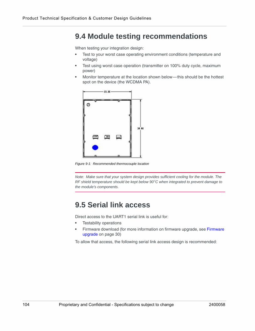
Product Technical Specification & Customer Design Guidelines
9.4 Module testing recommendations
When testing your integration design:
• Test to your worst case operating environment conditions (temperature and voltage)
• Test using worst case operation (transmitter on 100% duty cycle, maximum power)
• Monitor temperature at the location shown below—this should be the hottest spot on the device (the WCDMA PA).
Figure 9-1: Recommended thermocouple location
Note: Make sure that your system design provides sufficient cooling for the module. The RF shield temperature should be kept below 90°C when integrated to prevent damage to the module’s components.
9.5 Serial link access
Direct access to the UART1 serial link is useful for:
• Testability operations
• Firmware download (for more information on firmware upgrade, see Firmware upgrade on page 30)
To allow that access, the following serial link access design is recommended:
104 Proprietary and Confidential - Specifications subject to change 2400058
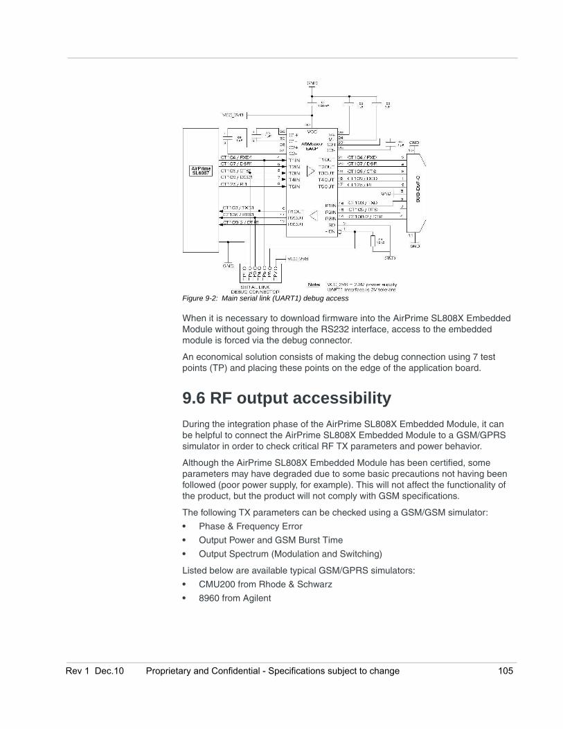
Figure 9-2: Main serial link (UART1) debug access
When it is necessary to download firmware into the AirPrime SL808X Embedded Module without going through the RS232 interface, access to the embedded module is forced via the debug connector.
An economical solution consists of making the debug connection using 7 test points (TP) and placing these points on the edge of the application board.
9.6 RF output accessibility
During the integration phase of the AirPrime SL808X Embedded Module, it can be helpful to connect the AirPrime SL808X Embedded Module to a GSM/GPRS simulator in order to check critical RF TX parameters and power behavior.
Although the AirPrime SL808X Embedded Module has been certified, some parameters may have degraded due to some basic precautions not having been followed (poor power supply, for example). This will not affect the functionality of the product, but the product will not comply with GSM specifications.
The following TX parameters can be checked using a GSM/GSM simulator:
• Phase & Frequency Error
• Output Power and GSM Burst Time
• Output Spectrum (Modulation and Switching)
Listed below are available typical GSM/GPRS simulators:
• CMU200 from Rhode & Schwarz
• 8960 from Agilent
Rev 1 Dec.10 Proprietary and Confidential - Specifications subject to change 105

Product Technical Specification & Customer Design Guidelines
Because of the high prices associated with GSM/GPRS simulators and the necessary GSM know-how to perform simulations, customers can check their applications in the Sierra Wireless laboratories. Contact the Sierra Wireless support team for more information.
106 Proprietary and Confidential - Specifications subject to change 2400058
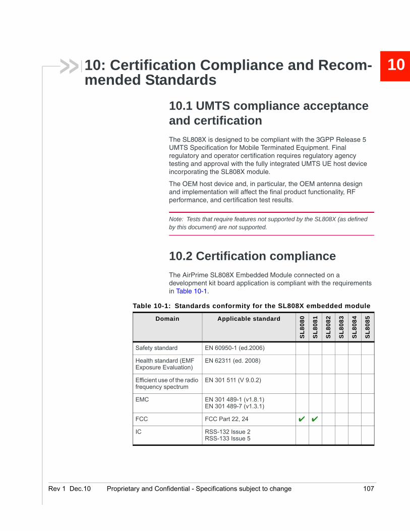
Rev 1 Dec
10
10: Certification Compliance and Recom-mended Standards10.1 UMTS compliance acceptance and certification
The SL808X is designed to be compliant with the 3GPP Release 5 UMTS Specification for Mobile Terminated Equipment. Final regulatory and operator certification requires regulatory agency testing and approval with the fully integrated UMTS UE host device incorporating the SL808X module.
The OEM host device and, in particular, the OEM antenna design and implementation will affect the final product functionality, RF performance, and certification test results.
Note: Tests that require features not supported by the SL808X (as defined by this document) are not supported.
10.2 Certification compliance
The AirPrime SL808X Embedded Module connected on a development kit board application is compliant with the requirements in Table 10-1.
Table 10-1: Standards conformity for the SL808X embedded module
Domain Applicable standard
SL
80
80
SL
80
81
SL
80
82
SL
80
83
SL
80
84
SL
80
85
Safety standard EN 60950-1 (ed.2006)
Health standard (EMF Exposure Evaluation)
EN 62311 (ed. 2008)
Efficient use of the radio frequency spectrum
EN 301 511 (V 9.0.2)
EMC EN 301 489-1 (v1.8.1)EN 301 489-7 (v1.3.1)
FCC FCC Part 22, 24
IC RSS-132 Issue 2RSS-133 Issue 5
.10 Proprietary and Confidential - Specifications subject to change 107
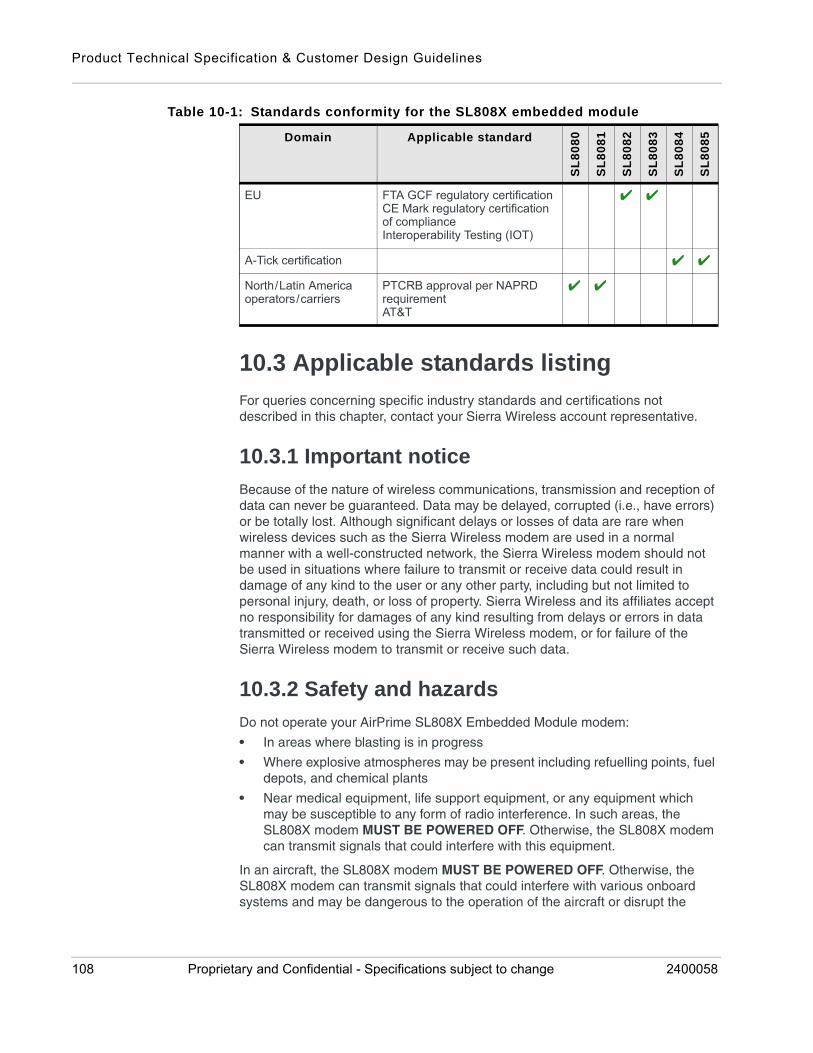
Product Technical Specification & Customer Design Guidelines
10.3 Applicable standards listing
For queries concerning specific industry standards and certifications not described in this chapter, contact your Sierra Wireless account representative.
10.3.1 Important notice
Because of the nature of wireless communications, transmission and reception of data can never be guaranteed. Data may be delayed, corrupted (i.e., have errors) or be totally lost. Although significant delays or losses of data are rare when wireless devices such as the Sierra Wireless modem are used in a normal manner with a well-constructed network, the Sierra Wireless modem should not be used in situations where failure to transmit or receive data could result in damage of any kind to the user or any other party, including but not limited to personal injury, death, or loss of property. Sierra Wireless and its affiliates accept no responsibility for damages of any kind resulting from delays or errors in data transmitted or received using the Sierra Wireless modem, or for failure of the Sierra Wireless modem to transmit or receive such data.
10.3.2 Safety and hazards
Do not operate your AirPrime SL808X Embedded Module modem:
• In areas where blasting is in progress
• Where explosive atmospheres may be present including refuelling points, fuel depots, and chemical plants
• Near medical equipment, life support equipment, or any equipment which may be susceptible to any form of radio interference. In such areas, the SL808X modem MUST BE POWERED OFF. Otherwise, the SL808X modem can transmit signals that could interfere with this equipment.
In an aircraft, the SL808X modem MUST BE POWERED OFF. Otherwise, the SL808X modem can transmit signals that could interfere with various onboard systems and may be dangerous to the operation of the aircraft or disrupt the
EU FTA GCF regulatory certificationCE Mark regulatory certification of complianceInteroperability Testing (IOT)
A-Tick certification
North/Latin America operators/carriers
PTCRB approval per NAPRD requirementAT&T
Table 10-1: Standards conformity for the SL808X embedded module
Domain Applicable standard
SL
80
80
SL
80
81
SL
80
82
SL
80
83
SL
80
84
SL
80
85
108 Proprietary and Confidential - Specifications subject to change 2400058
cellular network. Use of a cellular phone in an aircraft is illegal in some jurisdictions. Failure to observe this instruction may lead to suspension or denial of cellular telephone services to the offender, or legal action or both.
Some airlines may permit the use of cellular phones while the aircraft is on the ground and the door is open. The SL808X modem may be used normally at this time.
10.3.3 Important compliance information for North American users
The AirPrime SL808X Embedded Module has been granted modular approval for mobile applications. Integrators may use this device in their final products without additional FCC/IC (Industry Canada) certification if they meet the following conditions. Otherwise, additional FCC/IC approvals must be obtained.
1. At least 20 cm separation distance between the antenna and the user’s body must be maintained at all times.
2. To comply with FCC / IC regulations limiting both maximum RF output power and human exposure to RF radiation, the maximum antenna gain including cable loss in a mobile-only exposure condition must not exceed 5 dBi in the cellular band and 3 dBi in the PCS band.
3. The AirPrime SL808X Embedded Module and its antenna must not be co-located or operating in conjunction with any other transmitter or antenna within a host device.
4. A label must be affixed to the outside of the end product into which the AirPrime SL808X Embedded Module is incorporated, with a statement similar to the following:· For SL8080:
This device contains FCC ID: N7NSL8080This equipment contains equipment certified under IC: 2417C-SL8080
· For SL8081: This device contains FCC ID: N7NSL8081This equipment contains equipment certified under IC: 2417C-SL8081
5. A user manual with the end product must clearly indicate the operating requirements and conditions that must be observed to ensure compliance with current FCC / IC RF exposure guidelines.
The end product with an AirPrime SL808X Embedded Module may also need to pass the FCC Part 15 unintentional emission testing requirements and be properly authorized per FCC Part 15.
Note: If this module is intended for use in a portable device, you are responsible for separate approval to satisfy the SAR requirements of FCC Part 2.1093 and IC RSS-102.
Rev 1 Dec.10 Proprietary and Confidential - Specifications subject to change 109
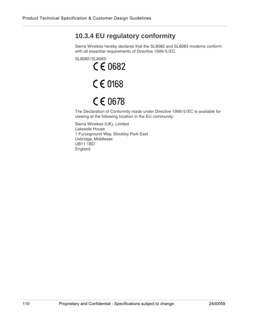
Product Technical Specification & Customer Design Guidelines
10.3.4 EU regulatory conformity
Sierra Wireless hereby declares that the SL8082 and SL8083 modems conform with all essential requirements of Directive 1999/5/EC.
SL8082/SL8083:
The Declaration of Conformity made under Directive 1999/5/EC is available for viewing at the following location in the EU community:
Sierra Wireless (UK), LimitedLakeside House1 Furzeground Way, Stockley Park EastUxbridge, MiddlesexUB11 1BDEngland
110 Proprietary and Confidential - Specifications subject to change 2400058
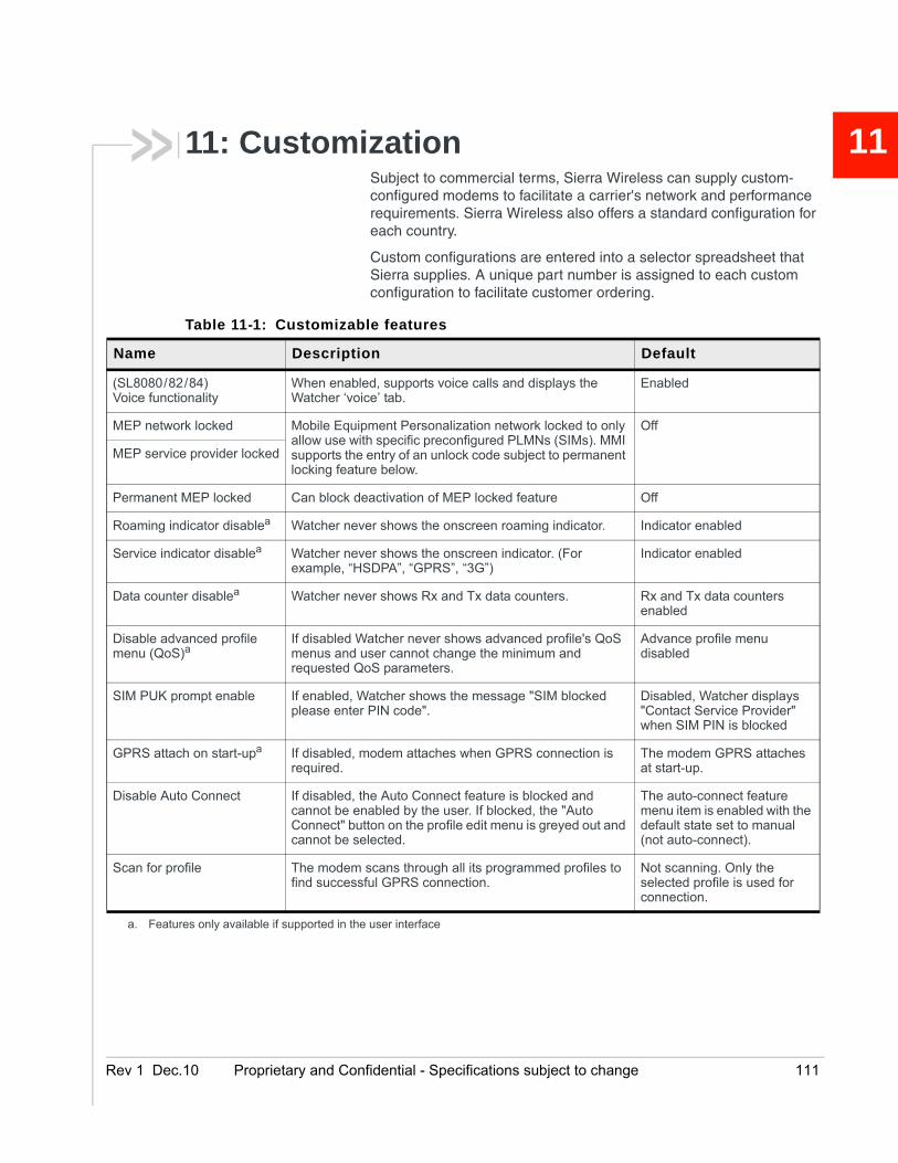
Rev 1 Dec
11
Name
(SL8080/8Voice func
MEP netw
MEP servi
Permanen
Roaming i
Service ind
Data coun
Disable admenu (QoS
SIM PUK p
GPRS atta
Disable Au
Scan for p
a. Feat
11: CustomizationSubject to commercial terms, Sierra Wireless can supply custom-configured modems to facilitate a carrier's network and performance requirements. Sierra Wireless also offers a standard configuration for each country.
Custom configurations are entered into a selector spreadsheet that Sierra supplies. A unique part number is assigned to each custom configuration to facilitate customer ordering.
Table 11-1: Customizable features
Description Default
2/84)tionality
When enabled, supports voice calls and displays the Watcher ‘voice’ tab.
Enabled
ork locked Mobile Equipment Personalization network locked to only allow use with specific preconfigured PLMNs (SIMs). MMI supports the entry of an unlock code subject to permanent locking feature below.
Off
ce provider locked
t MEP locked Can block deactivation of MEP locked feature Off
ndicator disablea Watcher never shows the onscreen roaming indicator. Indicator enabled
icator disablea Watcher never shows the onscreen indicator. (For example, “HSDPA”, “GPRS”, “3G”)
Indicator enabled
ter disablea Watcher never shows Rx and Tx data counters. Rx and Tx data counters enabled
vanced profile )a
If disabled Watcher never shows advanced profile's QoS menus and user cannot change the minimum and requested QoS parameters.
Advance profile menu disabled
rompt enable If enabled, Watcher shows the message "SIM blocked please enter PIN code".
Disabled, Watcher displays "Contact Service Provider" when SIM PIN is blocked
ch on start-upa If disabled, modem attaches when GPRS connection is required.
The modem GPRS attaches at start-up.
to Connect If disabled, the Auto Connect feature is blocked and cannot be enabled by the user. If blocked, the "Auto Connect" button on the profile edit menu is greyed out and cannot be selected.
The auto-connect feature menu item is enabled with the default state set to manual (not auto-connect).
rofile The modem scans through all its programmed profiles to find successful GPRS connection.
Not scanning. Only the selected profile is used for connection.
ures only available if supported in the user interface
.10 Proprietary and Confidential - Specifications subject to change 111

Product Technical Specification & Customer Design Guidelines
112 Proprietary and Confidential - Specifications subject to change 2400058
Rev 1 Dec
12
12: Safety Recommendations(For Information Only)For the efficient and safe operation of your GSM application based on the AirPrime SL808X Embedded Module, please read the following information carefully.
12.1 RF safety
12.1.1 General
Your GSM terminal is based on the GSM standard for cellular technology. The GSM standard is spread all over the world. It covers Europe, Asia and some parts of America and Africa. This is the most used telecommunication standard.
Your GSM terminal is actually a low power radio transmitter and receiver. It sends out as well as receives radio frequency energy. When you use your GSM application, the cellular system which handles your calls controls both the radio frequency and the power level of your cellular modem.
12.1.2 Exposure to RF energy
There has been some public concern about possible health effects of using GSM terminals. Although research on health effects from RF energy has focused on the current RF technology for many years, scientists have begun research regarding newer radio technologies, such as GSM. After existing research had been reviewed, and after compliance to all applicable safety standards had been tested, it has been concluded that the product was fitted for use.
If you are concerned about exposure to RF energy, there are things you can do to minimize exposure. Obviously, limiting the duration of your calls will reduce your exposure to RF energy. In addition, you can reduce RF exposure by operating your cellular terminal efficiently by following the guidelines below.
12.1.3 Efficient terminal operation
For your GSM terminal to operate at the lowest power level, consistent with satisfactory call quality:
If your terminal has an extendable antenna, extend it fully. Some models allow you to place a call with the antenna retracted. However your GSM terminal operates more efficiently with the antenna when it is fully extended.
.10 Proprietary and Confidential - Specifications subject to change 113

Product Technical Specification & Customer Design Guidelines
Do not hold the antenna when the terminal is "IN USE". Holding the antenna affects call quality and may cause the modem to operate at a higher power level than needed.
12.1.4 Antenna care and replacement
Do not use the GSM terminal with a damaged antenna. If a damaged antenna comes into contact with the skin, a minor burn may result. Replace a damaged antenna immediately. You may repair antenna to yourself by following the instructions provided to you. If so, use only a manufacturer-approved antenna. Otherwise, have your antenna repaired by a qualified technician.
Buy or replace the antenna only from the approved suppliers list. Using unauthorized antennas, modifications or attachments could damage the terminal and may contravene local RF emission regulations or invalidate type approval.
12.2 General safety
12.2.1 Driving
Check the laws and the regulations regarding the use of cellular devices in the area where you have to drive as you always have to comply with them. When using your GSM terminal while driving, please:
• give full attention to driving,
• pull off the road and park before making or answering a call if driving condi-tions so require.
12.2.2 Electronic devices
Most electronic equipment, for example in hospitals and motor vehicles is shielded from RF energy. However, RF energy may affect some improperly shielded electronic equipment.
12.2.3 Vehicle electronic equipment
Check with your vehicle manufacturer representative to determine if any on-board electronic equipment is adequately shielded from RF energy.
12.2.4 Medical electronic equipment
Consult the manufacturer of any personal medical devices (such as pacemakers, hearing aids, etc...) to determine if they are adequately shielded from external RF energy.
Turn your terminal OFF in health care facilities when any regulations posted in the area instruct you to do so. Hospitals or health care facilities may be using RF monitoring equipment.
114 Proprietary and Confidential - Specifications subject to change 2400058
12.2.5 Aircraft
Turn your terminal OFF before boarding any aircraft.
• Use it on the ground only with crew permission.
• Do not use it in the air.
To prevent possible interference with aircraft systems, Federal Aviation Administration (FAA) regulations require you should have prior permission from a crew member to use your terminal while the aircraft is on the ground. To prevent interference with cellular systems, local RF regulations prohibit using your modem while airborne.
12.2.6 Children
Do not allow children to play with your GSM terminal. It is not a toy. Children could hurt themselves or others (by poking themselves or others in the eye with the antenna, for example). Children could damage the modem, or make calls that increase your modem bills.
12.2.7 Blasting areas
To avoid interfering with blasting operations, turn your unit OFF when you are in a "blasting area" or in areas posted: "turn off two-way radio". Construction crew often uses remote control RF devices to set off explosives.
12.2.8 Potentially explosive atmospheres
Turn your terminal OFF when in any area with a potentially explosive atmosphere. Though it is rare, but your modem or its accessories could generate sparks. Sparks in such areas could cause an explosion or fire resulting in bodily injuries or even death.
Areas with a potentially explosive atmosphere are often, but not always, clearly marked. They include fuelling areas such as petrol stations; below decks on boats; fuel or chemical transfer or storage facilities; and areas where the air contains chemicals or particles, such as grain, dust, or metal powders.
Do not transport or store flammable gas, liquid, or explosives, in the compartment of your vehicle which contains your terminal or accessories.
Before using your terminal in a vehicle powered by liquefied petroleum gas (such as propane or butane) ensure that the vehicle complies with the relevant fire and safety regulations of the country in which the vehicle is used.
Rev 1 Dec.10 Proprietary and Confidential - Specifications subject to change 115

Product Technical Specification & Customer Design Guidelines
116 Proprietary and Confidential - Specifications subject to change 2400058
Rev 1 Dec
13
13: Connector and Peripheral Device References13.1 JTAG connector
• Sierra Wireless suggests that a MOLEX ZIF connector be applied to your design to enable debugging/testing of devices by Sierra Wireless in the event of platform issues (see http://www.molex.com).
.10 Proprietary and Confidential - Specifications subject to change 117

Product Technical Specification & Customer Design Guidelines
118 Proprietary and Confidential - Specifications subject to change 2400058
Rev 1 Dec
14
14: References14.1 Web site support
For additional documents describing embedded module design, usage, and integration issues, visit www.sierrawireless.com.
14.2 Reference documents
14.2.1 Sierra Wireless documents
The following Sierra Wireless documents are provided in your documentation package, or are available from www.sierrawireless.com:
[1] SL Dev Kit Quick Start Guide (TBD)
[2] AirCard/AirPrime UMTS Devices Supported AT Command Reference
Document 2130617
[3] AirPrime MC8xxx Embedded Modules Extended AT Command Reference
Document 2130616
[4] AirPrime UMTS MiniCard CnS Reference
Document 2130602
[5] Sierra Wireless Reliability Specification
Document 4110485
[6] AirCard/AirPrime USB Driver Developer’s Guide
Document 2130634
[7] Customer Process Guidelines—AirPrime SL Series
Document WM_DEV_LG_PTS_001
14.2.2 Industry/other documents
The following non-Sierra Wireless references are not included in your documentation package:
[8] Universal Serial Bus Specification, Rev 2.0
[9] 3GPP TS 34.108
.10 Proprietary and Confidential - Specifications subject to change 119
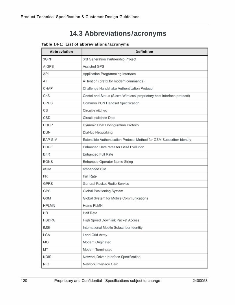
Product Technical Specification & Customer Design Guidelines
14.3 Abbreviations/acronyms
Table 14-1: List of abbreviations / acronyms
Abbreviation Definition
3GPP 3rd Generation Partnership Project
A-GPS Assisted GPS
API Application Programming Interface
AT ATtention (prefix for modem commands)
CHAP Challenge Handshake Authentication Protocol
CnS Contol and Status (Sierra Wireless’ proprietary host interface protocol)
CPHS Common PCN Handset Specification
CS Circuit-switched
CSD Circuit-switched Data
DHCP Dynamic Host Configuration Protocol
DUN Dial-Up Networking
EAP-SIM Extensible Authentication Protocol Method for GSM Subscriber Identity
EDGE Enhanced Data rates for GSM Evolution
EFR Enhanced Full Rate
EONS Enhanced Operator Name String
eSIM embedded SIM
FR Full Rate
GPRS General Packet Radio Service
GPS Global Positioning System
GSM Global System for Mobile Communications
HPLMN Home PLMN
HR Half Rate
HSDPA High Speed Downlink Packet Access
IMSI International Mobile Subscriber Identity
LGA Land Grid Array
MO Modem Originated
MT Modem Terminated
NDIS Network Driver Interface Specification
NIC Network Interface Card
120 Proprietary and Confidential - Specifications subject to change 2400058
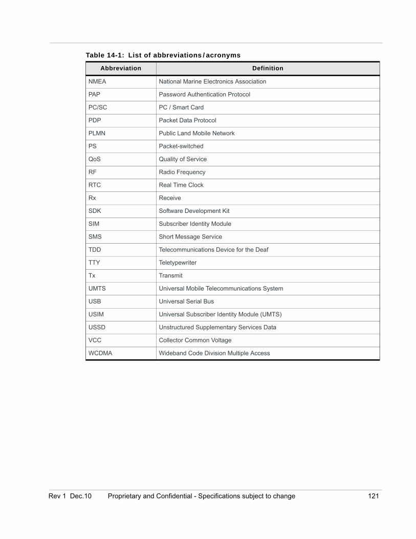
NMEA National Marine Electronics Association
PAP Password Authentication Protocol
PC/SC PC / Smart Card
PDP Packet Data Protocol
PLMN Public Land Mobile Network
PS Packet-switched
QoS Quality of Service
RF Radio Frequency
RTC Real Time Clock
Rx Receive
SDK Software Development Kit
SIM Subscriber Identity Module
SMS Short Message Service
TDD Telecommunications Device for the Deaf
TTY Teletypewriter
Tx Transmit
UMTS Universal Mobile Telecommunications System
USB Universal Serial Bus
USIM Universal Subscriber Identity Module (UMTS)
USSD Unstructured Supplementary Services Data
VCC Collector Common Voltage
WCDMA Wideband Code Division Multiple Access
Table 14-1: List of abbreviations / acronyms
Abbreviation Definition
Rev 1 Dec.10 Proprietary and Confidential - Specifications subject to change 121