product specification for lcd module
TRANSCRIPT

PRODUCT SPECIFICATION FOR LCD MODULE
MODULE NO. : ET-G12864F REVERSION : V3 TYPE : COB
Customer Approval:
PREPARED BY DATE
CHECKED BY DATE
APPROVED BY DATE

LCD MODULE
ET-G12864FV3 JUNE.26.2010
SHEN ZHEN ET TECHNOLOGY CO., LTD. Tel: 86-755- 88834445 Fax: 86-755-88834446 E-mail: east@eastet .com Http//www.eastet.com
- 1 -
DOCUMENT REVISION HISTORY
VERION DATE DESCRIPTION CHANGED BY V1 MAY,8,2007 First issue YE V2 APR.14.2009 Add Software Design Guide Retsen V3 JUNE.26.2010 Modify specification Sookey

LCD MODULE
ET-G12864FV3 JUNE.26.2010
SHEN ZHEN ET TECHNOLOGY CO., LTD. Tel: 86-755- 88834445 Fax: 86-755-88834446 E-mail: east@eastet .com Http//www.eastet.com
- 2 -
1. General Specifications
Item Standard Value UnitNumber of dots 128(W)X64(H) dotsDisplay Pattern Dot-Graphic Character Digits with ICON _____
Module Dimension 93(W) X70(H) X 11.0(T) mmViewing Area 72.00(W) X 40.00(H) mmActive Area 66.52(W) x 33.24(H) mmDOT Size 0.48(W) x 0.48(H) mmDOT Pitch 0.52(W) x 0.52(H) mm
LCD Type
TN,Positive TN, Negative HTN, Positive HTN, Negative STN, Yellow-Green STN, Gray STN, Blue FSTN, Positive FSTN, Negative Color STN FM LCD
Polarizer Type Transmissive Reflective Transflective Anti-Glare View Direction 6H 12H _________
Operation Voltage 3.0(3.3) 5.0 _________ V DC-DC Converter Build-in External
LCD Controller & Driver ST7920 &ST7921 LCD Driving Method 1/32duty, 1/6bias
Interface Type 6800 8080 I2C Serial SPI _________
Backlight Type LED CCFL EL no Backlight ____
Backlight Led Position Bottom Side Backlight Color Yellow-Green White Amber Blue Red
_____
Woke Life(at ambient temperature and moisture)
30000(Side Led、CCFL) 20000(Bottom Led) 5000(EL)
hrs
Supply current(type) <50(Side Led) <360(Bottom Led) _____ mA
EL/CCFL Driver type Build-in External Operation Temperature(oC) -20-70 (TOPL – TOPH) deg..Storage Temperature (oC) -30-80 (TSTL -- TSTH) deg..
Note: Label “ ” means the option selected.

LCD MODULE
ET-G12864FV3 JUNE.26.2010
SHEN ZHEN ET TECHNOLOGY CO., LTD. Tel: 86-755- 88834445 Fax: 86-755-88834446 E-mail: east@eastet .com Http//www.eastet.com
- 3 -
2. External Dimensions
128 * 64 DOTS
3. Block Diagram

LCD MODULE
ET-G12864FV3 JUNE.26.2010
SHEN ZHEN ET TECHNOLOGY CO., LTD. Tel: 86-755- 88834445 Fax: 86-755-88834446 E-mail: east@eastet .com Http//www.eastet.com
- 4 -
128 X 32 DOTS
128 X 32 DOTS
SEGMENT DRIVER
LED BACKLIGHTLED A A
R
LED KK
DB0-DB7
EPSB
R/WRS
/RST
VSSVDD
SEGMENT DRIVER
32COM
32COMCONTROLLER
ST7920
SEG64 SEG96 SEG96
4. Pin Description
Pin Name Level Function 1 VSS P GND(0V) 2 VDD P Power supply for logic and LCD(2.7V to 5.5V). 3 NC/VO - NC / Voltage level for LCD contrast adjustment.
4 RS(CS) I
Register select 0: select instruction write, busy flag read,address counter read 1: select data write, read (Chip select) for serial mode 1: chip enable 0: chip disable
5 RW(STD) I Read write control 0: write 1: read (serial data input)
6 E(SCLK) I Enable trigger (serial clock)
7-14 DB0-DB7 I/O data bus
15 PSB I Interface selection: 0: serial mode 1: 8/4-bits parallel bus mode
16 NC - NC 17 /RST I System reset low active 18 NC - NC 19 A P Anode for LED Backlight 20 K P Cathode for LED Backlight
5. Absolute Maximum Ratings Characteristics Symbol Value
Power Supply Voltage VDD -0.3V to +5.5V LCD Driver Voltage VLCD -0.3V to +7.0V
Input Voltage VIN -0.3V to VDD+0.3V

LCD MODULE
ET-G12864FV3 JUNE.26.2010
SHEN ZHEN ET TECHNOLOGY CO., LTD. Tel: 86-755- 88834445 Fax: 86-755-88834446 E-mail: east@eastet .com Http//www.eastet.com
- 5 -
Operating Temperature TA -20oC to + 85oC Storage Temperature TSTO -55oC to + 125oC
6. DC Characteristics
( TA = 25 oC , VDD = 2.7 V – 4.5 V ) Symbol Characteristics TestCondition Min. Typ. Max. Unit
VDD OperatingVoltage - 2.7 - 5.5 V VLCD LCD Voltage V0-VSS 3.0 - 7 V ICC Power Supply Current fOSC =530KHz,VDD=3.0V
Rf=18KΩ - 0.20 0.45 mA
VIH1 Input High Voltage (Except OSC1) - 0.7VDD - VDD V
VIL1 Input Low Voltage (Except OSC1) - -0.3 - 0.6 V
VIH2 Input High Voltage (OSC1) - VDD –1 - VDD V
VIL2 Input Low Voltage (OSC1) - - - 1.0 V
VOH1 Output High Voltage (DB0 - DB7) IOH = -0.1mA 0.8VDD - VDD V
VOL1 Output Low Voltage (DB0 - DB7) IOL = 0.1mA - - 0.1 V
VOH2 Output High Voltage (Except DB0 - DB7) IOH = -0.04mA 0.8VDD - VDD V
VOL2 Output Low Voltage (Except DB0 - DB7) IOL = 0.04mA - - 0.1VDD V
ILEAK Input Leakage Current VIN = 0V to VDD -1 - 1 μAIPUP Pull Up MOS Current VDD = 3V 22 27 32 μA
( TA = 25 oC, VDD = 4.5 V - 5.5 V ) Symbol Characteristics TestCondition Min. Typ. Max. Unit
VDD OperatingVoltage - 4.5 - 5.5 V VLCD LCD Voltage V0-VSS 3.0 - 7 V ICC Power Supply Current fOSC =530KHz,VDD=3.0V
Rf=18KΩ - 0.45 0.75 mA
VIH1 Input High Voltage (Except OSC1) - 0.7VDD - VDD V
VIL1 Input Low Voltage (Except OSC1) - -0.3 - 0.6 V
VIH2 Input High Voltage (OSC1) - VDD –1 - VDD V
VIL2 Input Low Voltage (OSC1) - - - 1.0 V
VOH1 Output High Voltage (DB0 - DB7) IOH = -0.1mA 0.8VDD - VDD V
VOL1 Output Low Voltage (DB0 - DB7) IOL = 0.1mA - - 0.4 V
VOH2 Output High Voltage (Except DB0 - DB7) IOH = -0.04mA 0.8VDD - VDD V
VOL2 Output Low Voltage (Except DB0 - DB7) IOL = 0.04mA - - 0.1VDD V
ILEAK Input Leakage Current VIN = 0V to VDD -1 - 1 μAIPUP Pull Up MOS Current VDD = 5V 75 80 85 μA
7. AC Characteristics
Parallel Mode Interface (TA = 25oC, VDD = 4.5V)
Symbol Characteristics Test Condition Min. Typ. Max. Unit
Internal Clock Operation

LCD MODULE
ET-G12864FV3 JUNE.26.2010
SHEN ZHEN ET TECHNOLOGY CO., LTD. Tel: 86-755- 88834445 Fax: 86-755-88834446 E-mail: east@eastet .com Http//www.eastet.com
- 6 -
fOSC OSC Frequency R = 33KΩ 480 540 600 KHz
External Clock Operation
fEX External Frequency - 480 540 600 KHz
Duty Cycle - 45 50 55 %
TR,TF Rise/Fall Time - - - 0.2 μs
Write Mode (Writing data from MPU to ST7920)
TC Enable Cycle Time Pin E 1200 - - ns
TPW Enable Pulse Width Pin E 140 - - ns
TR,TF Enable Rise/Fall Time Pin E - - 25 ns
TAS Address Setup Time Pins: RS,RW,E 10 - - ns
TAH Address Hold Time Pins: RS,RW,E 20 - - ns
TDSW Data Setup Time Pins: DB0 - DB7 40 - - ns
TH Data Hold Time Pins: DB0 - DB7 20 - - ns
Read Mode (Reading Data from ST7920 to MPU)
TC Enable Cycle Time Pin E 1200 - - ns
TPW Enable Pulse Width Pin E 140 - - ns
TR,TF Enable Rise/Fall Time Pin E - - 25 ns
TAS Address Setup Time Pins: RS,RW,E 10 - - ns
TAH Address Hold Time Pins: RS,RW,E 20 - - ns
TDDR Data Delay Time Pins: DB0 - DB7 - - 100 ns
TH Data Hold Time Pins: DB0 - DB7 20 - - ns
Interface Mode with LCD Driver(ST7921)
TCWH Clock Pulse with High Pins: CL1, CL2 800 - - ns
TCWL Clock Pulse with Low Pins: CL1, CL2 800 - - ns
TCST Clock Setup Time Pins: CL1, CL2 500 - - ns
TSU Data Setup Time Pin: D 300 - - ns
TDH Data Hold Time Pin: D 300 - - ns
TDM M Delay Time Pin: M -1000 - 1000 ns
Parallel Mode Interface (TA = 25oC, VDD = 2.7V)
Symbol Characteristics Test Condition Min. Typ. Max. Unit
Internal Clock Operation
fOSC OSC Frequency R = 18KΩ 470 530 590 KHz
External Clock Operation
fEX External Frequency - 470 530 590 KHz
Duty Cycle - 45 50 55 %

LCD MODULE
ET-G12864FV3 JUNE.26.2010
SHEN ZHEN ET TECHNOLOGY CO., LTD. Tel: 86-755- 88834445 Fax: 86-755-88834446 E-mail: east@eastet .com Http//www.eastet.com
- 7 -
TR,TF Rise/Fall Time - - - 0.2 μs
Write Mode (Writing data from MPU to ST7920)
TC Enable Cycle Time Pin E 1800 - - ns
TPW Enable Pulse Width Pin E 160 - - ns
TR,TF Enable Rise/Fall Time Pin E - - 25 ns
TAS Address Setup Time Pins: RS,RW,E 10 - - ns
TAH Address Hold Time Pins: RS,RW,E 20 - - ns
TDSW Data Setup Time Pins: DB0 - DB7 40 - - ns
TH Data Hold Time Pins: DB0 - DB7 20 - - ns
Read Mode (Reading Data from ST7920 to MPU)
TC Enable Cycle Time Pin E 1800 - - ns
TPW Enable Pulse Width Pin E 320 - - ns
TR,TF Enable Rise/Fall Time Pin E - - 25 ns
TAS Address Setup Time Pins: RS,RW,E 10 - - ns
TAH Address Hold Time Pins: RS,RW,E 20 - - ns
TDDR Data Delay Time Pins: DB0 - DB7 - - 260 ns
TH Data Hold Time Pins: DB0 - DB7 20 - - ns
Interface Mode with LCD Driver(ST7921)
TCWH Clock Pulse with High Pins: CL1, CL2 800 - - ns
TCWL Clock Pulse with Low Pins: CL1, CL2 800 - - ns
TCST Clock Setup Time Pins: CL1, CL2 500 - - ns
TSU Data Setup Time Pin: D 300 - - ns
TDH Data Hold Time Pin: D 300 - - ns
TDM M Delay Time Pin: M -1000 - 1000 ns
Serial Mode Interface (TA = 25oC, VDD = 4.5V)
Symbol Characteristics Test Condition Min. Typ. Max. Unit
Internal Clock Operation
fOSC OSC Frequency R = 33KΩ 470 530 590 KHz
External Clock Operation
fEX External Frequency - 470 530 590 KHz
Duty Cycle - 45 50 55 %
TR,TF Rise/Fall Time - - - 0.2 μs
TSCYC Serial clock cycle Pin E 400 - - ns
TSHW SCLK high pulse width Pin E 200 - - ns
TSLW SCLK low pulse Pin E 200 - - ns

LCD MODULE
ET-G12864FV3 JUNE.26.2010
SHEN ZHEN ET TECHNOLOGY CO., LTD. Tel: 86-755- 88834445 Fax: 86-755-88834446 E-mail: east@eastet .com Http//www.eastet.com
- 8 -
width
TSDS SID data setup time Pins RW 40 - - ns
TSDH SID data hold time Pins RW 40 - - ns
TCSS CS setup time Pins RS 60 - - ns
TCSH CS hold time Pins RS 60 - - ns
Serial Mode Interface (TA = 25oC, VDD = 2.7V)
Symbol Characteristics Test Condition Min. Typ. Max. Unit
Internal Clock Operation
fOSC OSC Frequency R = 18KΩ 470 530 590 KHz
External Clock Operation
fEX External Frequency - 470 530 590 KHz
Duty Cycle - 45 50 55 %
TR,TF Rise/Fall Time - - - 0.2 μs
TSCYC Serial clock cycle Pin E 600 - - ns
TSHW SCLK high pulse width Pin E 300 - - ns
TSLW SCLK low pulse width Pin E 300 - - ns
TSDS SID data setup time Pins RW 40 - - ns
TSDH SID data hold time Pins RW 40 - - ns
TCSS CS setup time Pins RS 60 - - ns
TCSH CS hold time Pins RS 60 - - ns
External reset timing
XRESET pulse width Trw 10us
RESET start time Tres 50ns
8. Parallel 8 bit interface timing diagram

LCD MODULE
ET-G12864FV3 JUNE.26.2010
SHEN ZHEN ET TECHNOLOGY CO., LTD. Tel: 86-755- 88834445 Fax: 86-755-88834446 E-mail: east@eastet .com Http//www.eastet.com
- 9 -
MPU write data to ST7920
MPU read data from ST7920
Parallel interface : ST7920 is in parallel mode by pulling up PSB pin. And can select 8 bit or 4-bit bus interface by function set instruction DL control bit. MPU can control ( RS , RW , E , and DB0..DB7 ) pins to complete the data transmission. In 4-bit transfer mode, every 8 bits data or instruction is separated into 2 parts. Higher 4 bits(DB7~DB4)data will transfer First and placed into data pins(DB7~DB4). Lower 4 bits(DB3~DB0)data will transfer second and placed into data pins(DB7~DB4). (DB3~DB0) data pins are not used.
Timing Diagram of 8-bit Parallel Bus Mode Data Transfer

LCD MODULE
ET-G12864FV3 JUNE.26.2010
SHEN ZHEN ET TECHNOLOGY CO., LTD. Tel: 86-755- 88834445 Fax: 86-755-88834446 E-mail: east@eastet .com Http//www.eastet.com
- 10 -
Timing Diagram of 4-bit Parallel Bus Mode Data Transfer
9. Serial interface timing diagram
MPU write data to ST7920
Serial interface : ST7920 is in serial interface mode when pull down PSB pin. Two pins (SCLK and SID) are used to complete the data transfer. Only write data is available. When connecting several ST7920, chip selec(t CS)must be used. Only when(CS)is high the serial clock(SCLK)can be accepted. On the other hand, when chip select(CS)is low ST7920 serial counter and data will be reset. Transmission will be terminated and data will be cleared. Serial transfer counter is set to the first bit. For a minimal system with only one ST7920 and one MPU, only SCLK and SID pins are necessary. CS pin should pull to high. ST7920’s serial clock(SCLK)is asynchronous to the internal clock and is generated by MPU. When multiple instruction/data is transferred instruction execution time must be considered. Must wait for the previous instruction to finish before sending the next. ST7920 has no internal instruction buffer area. When starting a transmission a start byte is required. It consists of 5 consecutive 〝1〞(sync character). Serial transfer counter will be reset and synchronized. Following 2 bits for read/write(RW)and register/data select(RS). Last 4 bits is filled by 〝0〞。 After receiving the sync character and RW and RS bits, every 8 bits instruction/data will be separated into 2 groups. Higher 4 bits(DB7~DB4)will be placed in first section followed by 4 〝0〞. And lower 4 bits(DB3~DB0)will be placed in second section followed by 4 〝0〞.

LCD MODULE
ET-G12864FV3 JUNE.26.2010
SHEN ZHEN ET TECHNOLOGY CO., LTD. Tel: 86-755- 88834445 Fax: 86-755-88834446 E-mail: east@eastet .com Http//www.eastet.com
- 11 -
Timing Diagram of Serial Mode Data Transfer
10. Instruction Table ST7920 offers basic instruction set and extended instruction set: Instruction set 1: (RE=0: basic instruction)
code Instruction RS RW DB7 DB6 DB5 DB4 DB3 DB2 DB1 DB0
Description Exectime(540KHZ)
CLEAR 0 0 0 0 0 0 0 0 0 1 Fill DDRAM with "20H", and set DDRAM address counter (AC)to "00H" 1.6 ms
HOME 0 0 0 0 0 0 0 0 1 X Set DDRAM address counter(AC)to "00H", and put cursor to origin ;the content of DDRAM are not changed 72us
ENTRY MODE 0 0 0 0 0 0 0 1 I/D S Set cursor position and display shift when doing write or read operation 72us
DISPLAY ON/OFF 0 0 0 0 0 0 1 D C B
D=1: display ON C=1: cursor ON B=1: blink ON
72us
CURSOR DISPLAY
CONTROL 0 0 0 0 0 1 S/C R/L X X Cursor position and display shift control ;the content of DDRAM are not changed 72us
FUNCTION SET 0 0 0 0 1 DL X 0
RE X X DL=1 8-BIT interface DL=0 4-BIT interface RE=1: extended instruction RE=0: basic instruction
72us
SET CGRAM ADDR.
0 0 0 1 AC5 AC4 AC3 AC2 AC1 AC0 Set CGRAM address to address counter(AC) Make sure that in extended instruction SR=0 (scroll or RAM address select) 72us
SET DDRAM ADDR.
0 0 1 0 AC6 AC5 AC4 AC3 AC2 AC1 AC0 Set DDRAM address to address counter(AC)
AC6 is fixed to 0 72us
READ 0 1 BF AC6 AC5 AC4 AC3 AC2 AC1 AC0 Read busy flag(BF)for completion of internal operation, also 0us

LCD MODULE
ET-G12864FV3 JUNE.26.2010
SHEN ZHEN ET TECHNOLOGY CO., LTD. Tel: 86-755- 88834445 Fax: 86-755-88834446 E-mail: east@eastet .com Http//www.eastet.com
- 12 -
BUSY FLAG(BF)
& ADDR.
Read out the value of address counter(AC)
WRITE RAM 1 0 D7 D6 D5 D4 D3 D2 D1 D0 Write data to internal RAM
(DDRAM/CGRAM/IRAM/GDRAM) 72us
READ RAM 1 1 D7 D6 D5 D4 D3 D2 D1 D0 Read data from internal RAM (DDRAM/CGRAM/IRAM/GDRAM) 72us
Instruction set 2: (RE=1: extended instruction)
code Instruction RS RW DB7 DB6 DB5 DB4 DB3 DB2 DB1 DB0
Description Exectime(540KHZ)
STAND BY 0 0 0 0 0 0 0 0 0 1 Enter stand by mode, any other instruction can terminate (Com1..32 halted, only Com33 ICON can display) 72us
SCROLL or RAM
ADDR. SELECT
0 0 0 0 0 0 0 0 1 SR SR=1: enable vertical scroll position SR=0: enable IRAM address (extended instruction) SR=0: enable CGRAM address(basic instruction)
72us
REVERSE 0 0 0 0 0 0 0 1 R1 R0 Select 1 out of 4 line(in DDRAM)and decide whether to reverse the display by toggling this instructionR1,R0 initial value is 00 72us
SLEEP 0 0 0 0 0 0 1 SL X X SL=1: leave sleep mode SL=0: enter sleep mode 72us
EXTENDED FUNCTION
SET 0 0 0 0 1 DL X 1
RE G 0
DL=1 8-BIT interface DL=0 4-BIT interface RE=1: extended instruction set RE=0: basic instruction set G=1 :graphic display ON G=0 :graphic display OFF
72us
SET IRAM or SCROLL
ADDR
0 0 0 1 AC5 AC4 AC3 AC2 AC1 AC0 SR=1: AC5~AC0 the address of vertical scroll SR=0: AC3~AC0 the address of ICON RAM 72us
SET GRAPHIC
RAM ADDR.
0 0 1 0 AC6
0 AC5
0 AC4 AC3 AC2 AC1 AC0
Set GDRAM address to address counter(AC) First set vertical address and the horizontal address by consecutive writing Vertical address range AC6...AC0 Horizontal address range AC3…AC0
72us
Note: 1. Make sure that ST7920 is not in busy state by reading the busy flag before sending instruction or data. If use delay loop instead please make sure the delay time is enough. Please refer to the instruction execution time. 2. “RE”is the selection bit of basic and extended instruction set. Each time when altering the value of RE it will remain. There is no need to set RE every time when using the same group of instruction set.
GDRAM display coordinates and corresponding address

LCD MODULE
ET-G12864FV3 JUNE.26.2010
SHEN ZHEN ET TECHNOLOGY CO., LTD. Tel: 86-755- 88834445 Fax: 86-755-88834446 E-mail: east@eastet .com Http//www.eastet.com
- 13 -
012345678910111213141516171819202122232425262728293031
012345678910111213141516171819202122232425262728293031
0 1 7...
8 9 15...
...
...
GDRAM Horizontal address(X)
0123456789101112131415 0123456789101112131415 0123456789101112131415 Graphic RAM(GDRAM) Graphic display RAM supports 64x256 bits bit-mapped memory space. GDRAM address is set by writing 2 consecutive bytes for vertical address and horizontal address. Two-bytes data write to GDRAM for one address. Address counter will automatically increase by one for the next two-byte data. The procedure is as followings. 1. Set vertical address(Y)for GDRAM 2. Set horizontal address(X)for GDRAM 3. Write D15〜D8 to GDRAM (first byte) 4. Write D7〜D0 to GDRAM (second byte) CGRAM fonts and CGROM fonts can only be displayed in the start position of each address.
80H 81H 82H 83H 84H 85H 86H 87H 88H 89H 8AH 8BH 8CH 8DH 8EH 8FHH L H L H L H L H L H L H L H L H L H L H L H L H L H L H L H L
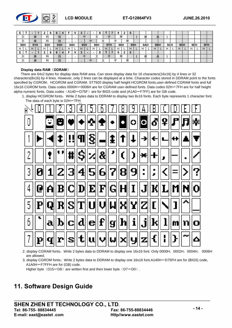
LCD MODULE
ET-G12864FV3 JUNE.26.2010
SHEN ZHEN ET TECHNOLOGY CO., LTD. Tel: 86-755- 88834445 Fax: 86-755-88834446 E-mail: east@eastet .com Http//www.eastet.com
- 14 -
E T - 1 2 8 6 4 F V 3 - - S T 7 9 2 0 尔 泰 科 技 . . 中 文 字 库 ( 液 晶 ) 尔 泰 科 技 . . . 中 文 字 库
90H 91H 92H 93H 94H 95H 96H 97H 98H 99H 9AH 9BH 9CH 9DH 9EH 9FHH L H L H L H L H L H L H L H L H L H L H L H L H L H L H L H LE T - 1 2 8 6 4 F V 3 - - S T 7 9 2 0 尔 泰 科 技 . . 中 文 字 库 ( 液 晶 ) 尔 泰 科 技 . . . 中 文 字 库
Display data RAM(DDRAM) There are 64x2 bytes for display data RAM area. Can store display data for 16 characters(16x16) by 4 lines or 32
characters(8x16) by 4 lines. However, only 2 lines can be displayed at a time. Character codes stored in DDRAM point to the fonts specified by CGROM,HCGROM and CGRAM. ST7920 display half height HCGROM fonts,user-defined CGRAM fonts and full 16x16 CGROM fonts. Data codes 0000H〜0006H are for CGRAM user-defined fonts. Data codes 02H〜7FH are for half height alpha numeric fonts. Data codes(A140〜D75F)are for BIG5 code and (A1A0〜F7FF) are for GB code.
1. display HCGROM fonts:Write 2 bytes data to DDRAM to display two 8x16 fonts. Each byte represents 1 character font. The data of each byte is 02H〜7FH.
2. display CGRAM fonts:Write 2 bytes data to DDRAM to display one 16x16 font. Only 0000H,0002H,0004H, 0006H
are allowed. 3. display CGROM fonts:Write 2 bytes data to DDRAM to display one 16x16 font.A140H〜D75FH are for (BIG5) code,
A1A0H〜F7FFH are for (GB) code. Higher byte(D15〜D8)are written first and then lower byte(D7〜D0).
11. Software Design Guide

LCD MODULE
ET-G12864FV3 JUNE.26.2010
SHEN ZHEN ET TECHNOLOGY CO., LTD. Tel: 86-755- 88834445 Fax: 86-755-88834446 E-mail: east@eastet .com Http//www.eastet.com
- 15 -
/********************************************* test code for reference show one R/W Enable Trigger Driver IC : ST7920 DATA BUS :8BIT 6800 MCU : W78E516B ********************************************/ #include "reg52.h" #define unsigned char unsigned char #define unsigned int unsigned int #define Lcd_Bus P1 #define FIRST_ADDR 0 //========================= sbit R_S = P3^0; sbit R_W = P3^1; sbit E1 = P3^2; //sbit E2 = P3^3; sbit RST = P3^4; sbit PSB = P3^5; //=========Delayus======== void Delayus(int count) unsigned int i,j; for(i=0;i<count;i++) for(j=0;j<10;j++); //=========CHECK BUSY====== void Check_Busy(void) R_S=0; R_W=1; Lcd_Bus=0xff; E1=1; while((Lcd_Bus&0x80)==0x80); E1=0; //========WRITE COMMAND==== void Write_Command (unsigned int com) Check_Busy(); R_S=0; R_W=0; Lcd_Bus=com; E1=1; Delayus(5); E1=0; Delayus(5); // Lcd_Bus=0XFF; //========WRITE DATA===== void Write_Data (unsigned int dat) Check_Busy(); R_S=1; R_W=0; Lcd_Bus=dat; E1 =1; Delayus(5);
<ST7920_I2C.H> /************************************************ Driver IC : ST7920 DATA BUS : I2C MCU : W78E516B Description: only write command&data
is different to 8bit 6800 mode *************************************************/ //========= Write Command========== void Write_Command(unsigned char cmd) unsigned char i; C_S = 1; SID = 1; for (i=0;i<5;i++) SCLK = 0; SCLK = 1; SCLK = 0; SID=0; for(i=0;i<3;i++) SCLK=1; SCLK=0; for(i=0;i<4;i++) cmd<<=1; SID=CY; SCLK=1; SCLK=0; SID=0; for(i=0;i<4;i++) SCLK=1; SCLK=0; for(i=0;i<4;i++) cmd<<=1; SID=CY; SCLK=1; SCLK=0; SID=0; for(i=0;i<4;i++) SCLK=1; SCLK=0; C_S = 0; Delay100us(1);
LCD MODULE
ET-G12864FV3 JUNE.26.2010
SHEN ZHEN ET TECHNOLOGY CO., LTD. Tel: 86-755- 88834445 Fax: 86-755-88834446 E-mail: east@eastet .com Http//www.eastet.com
- 16 -
E1=0; Delayus(5); // Lcd_Bus=0XFF; //=========Delayms===== void Delayms(int count) unsigned int i,j; for(i=0;i<count;i++) for(j=0;j<200;j++); /*********display_character_string===== ========Font:16X6Chinese characters=== ===22seg=7/line;128seg=8/line;192seg=12/line ==*/void hzkdisplay(unsigned char code *s) while(*s>0) Write_Data(*s); s++; Delayus(50); //===========initial code======== void INITIAL (void) Delayus(1); RST=0; Delayus(1); RST=1; Write_Command (0x34); Delayus(10); Write_Command (0x30); //set 8bit mode Delayus(10); Write_Command (0x01); //clear display, sp=00h Delayus(20); Write_Command (0x06); //set Cursor Delayus(10); Write_Command (0x0C); //Display on (no cursor,normal Pattern) Delayus(10); //======Clear CGRAM====== void Clear_CGRAM() unsigned char x,y; for(y=0;y<32;y++) for(x=0;x<16;x++) Write_Command(0x34); Write_Command(y+0x80); // Y address Write_Command(x+0x80); // X address Write_Command(0x30); Write_Data(0x00); Write_Data(0x00);
//============= Write Data ============== void Write_Data(unsigned char dat) unsigned char i; C_S = 1; SID = 1; for (i=0;i<5;i++) SCLK = 0; SCLK = 1; SCLK = 0; SID = 0; SCLK = 1; SCLK = 0; SID = 1; SCLK = 1; SCLK = 0; SID = 0; SCLK = 1; SCLK = 0; for (i=0;i<4;i++) dat<<=1; SID = CY; SCLK = 1; SCLK = 0; SID =0; for (i=0;i<4;i++) SCLK = 0; SCLK = 1; SCLK = 0; for (i=0;i<4;i++) dat<<=1; SID = CY; SCLK = 1; SCLK = 0; SID = 0; for (i=0;i<4;i++) SCLK = 1; SCLK = 0; C_S = 0; Delay100us(1);

LCD MODULE
ET-G12864FV3 JUNE.26.2010
SHEN ZHEN ET TECHNOLOGY CO., LTD. Tel: 86-755- 88834445 Fax: 86-755-88834446 E-mail: east@eastet .com Http//www.eastet.com
- 17 -
//========main menu======== void Main_menu() Write_Command(0x01); Delayus(5); Write_Command(0x80); //first line hzkdisplay("深圳市尔泰科技有限公司"); Write_Command(0x90); //first line hzkdisplay("http://www.eastet.com "); Write_Command(0xa0); //third line hzkdisplay(" 图形点阵显示模块 "); Write_Command(0xb0); //forth line hzkdisplay("Equipment initial ... "); //=========Clear Display========== void Clrscreen() Write_Command(0x01); Delayus(10); //===========main test======== void main() unsigned char i; PSB=1; INITIAL (); Delayus(500); while(1) Main_menu(); //display Main_menu Clear_CGRAM(); //clear CGRAM Clrscreen(); //transfer DDRAM Character below //display : SHENZHEN ET TEC.CO.,LTD Write_Command(0x80); Write_Data(0x53); /*S*/ Write_Data(0x48); /*H*/ Write_Data(0x45); /*E*/ Write_Data(0x4E); /*N*/ Write_Data(0x5A); /*Z*/ Write_Data(0x48); /*H*/ Write_Data(0x45); /*E*/ Write_Data(0x4E); /*N*/ Write_Data(0x20); /*SPACE*/ Write_Data(0x45); /*E*/ Write_Data(0x54); /*T Write_Data(0x20); /*SPACE*/ Write_Data(0x54); /*T*/ Write_Data(0x45); /*E*/ Write_Data(0x43); /*C*/ Write_Data(0x2E); /*. */ Write_Data(0x43); /*C*/ Write_Data(0x4F); /*0*/ Write_Data(0x2C); /*, */ Write_Data(0x4C); /*L*/ Write_Data(0x54); /*T*/ Write_Data(0x44); /*D*/

LCD MODULE
ET-G12864FV3 JUNE.26.2010
SHEN ZHEN ET TECHNOLOGY CO., LTD. Tel: 86-755- 88834445 Fax: 86-755-88834446 E-mail: east@eastet .com Http//www.eastet.com
- 18 -
Write_Data(0x20);//returnDDRAM initial address Delayus(800); Clear_CGRAM(); //clear CGRAM Clrscreen(); //clear display Delayus(100); //DISPLAY SHIFT CONTROL Main_menu(); Delayus(300); for(i=0;i<10;i++) //move 10 times Write_Command(0x18); Delayms(100); //reverse video control Main_menu(); Write_Command(0x36); Write_Command(0x04); //first line reverse display Delayms(500); Write_Command(0x04); //first line normal display Delayms(500); Write_Command(0x05); //second line reverse display Delayms(500); Write_Command(0x05); //second line normal display Delayms(500); Clrscreen(); //Clear display Clear_CGRAM();
LCD MODULE
ET-G12864FV3 JUNE.26.2010
SHEN ZHEN ET TECHNOLOGY CO., LTD. Tel: 86-755- 88834445 Fax: 86-755-88834446 E-mail: east@eastet .com Http//www.eastet.com
- 19 -
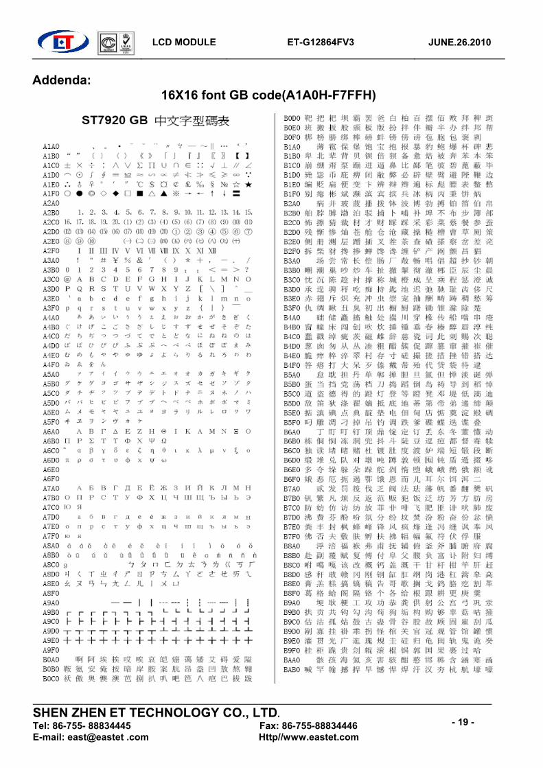
Addenda: 16X16 font GB code(A1A0H-F7FFH)

LCD MODULE
ET-G12864FV3 JUNE.26.2010
SHEN ZHEN ET TECHNOLOGY CO., LTD. Tel: 86-755- 88834445 Fax: 86-755-88834446 E-mail: east@eastet .com Http//www.eastet.com
- 20 -

LCD MODULE
ET-G12864FV3 JUNE.26.2010
SHEN ZHEN ET TECHNOLOGY CO., LTD. Tel: 86-755- 88834445 Fax: 86-755-88834446 E-mail: east@eastet .com Http//www.eastet.com
- 21 -

LCD MODULE
ET-G12864FV3 JUNE.26.2010
SHEN ZHEN ET TECHNOLOGY CO., LTD. Tel: 86-755- 88834445 Fax: 86-755-88834446 E-mail: east@eastet .com Http//www.eastet.com
- 22 -

LCD MODULE
ET-G12864FV3 JUNE.26.2010
SHEN ZHEN ET TECHNOLOGY CO., LTD. Tel: 86-755- 88834445 Fax: 86-755-88834446 E-mail: east@eastet .com Http//www.eastet.com
- 23 -