lcd module specification - display future€¦ · lcd module specification model : mi240160e-g...
TRANSCRIPT
LCD MODULE SPECIFICATION
Model : MI240160E-G
Revision 0.0 Engineering Date Our Reference
MULTI-INNO TECHNOLOGY CO., LTD.

RECORDS OF REVISION
Date Ver. Description Page Design by
2008/03/19 0.0
NEW SAMPLE -
P.2 MULTI-INNO TECHNOLOGY CO.,LTD.
MODULE NO.: MI240160E-G Ver 0.0

Contents
1. SPECIFICATIONS 1.1 Features 1.2 Mechanical Specifications 1.3 Absolute Maximum Ratings 1.4 DC Electrical Characteristics 1.5 Optical Characteristics 1.6 Backlight Characteristics
2. MODULE STRUCTURE 2.1 Counter Drawing 2.2 Interface Pin Description 2.3 Timing Characteristics 2.4 Display Command
3. QUALITY ASSURANCE SYSTEM 3.1 Quality Assurance Flow Chart 3.2 Inspection Specification
4. RELIABILITY TEST 4.1 Reliability Test Condition
5. PRECAUTION RELATING PRODUCT HANDLING 5.1 Safety 5.2 Handling 5.3 Storage 5.4 Terms of Warranty
6. PACKING Specification
Note: For detailed information please refer to IC data sheet: Controller --- ST7529-G
P.3 MULTI-INNO TECHNOLOGY CO.,LTD.
MODULE NO.: MI240160E-G Ver 0.0
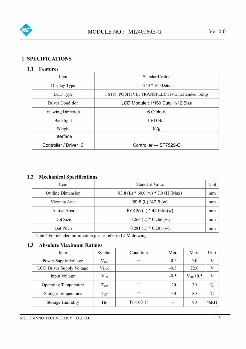
1. SPECIFICATIONS
1.1 Features Item Standard Value
Display Type 240 * 160 Dots
LCD Type FSTN .POSITIVE, TRANSFLECTIVE .Extended Temp
Driver Condition LCD Module : 1/160 Duty, 1/12 Bias
Viewing Direction 6 O’clock
Backlight LED B/L
Weight 52g
Interface -
Controller / Driver IC Controller --- ST7529-G
1.2 Mechanical Specifications Item Standard Value Unit
Outline Dimension 83.8 (L) * 60.0 (w) * 7.0 (H)(Max) mm
Viewing Area 69.6 (L) *47.6 (w) mm
Active Area 67.425 (L) * 44.945 (w) mm
Dot Size 0.266 (L) * 0.266 (w) mm
Dot Pitch 0.281 (L) * 0.281 (w) mm Note�For detailed information please refer to LCM drawing
1.3 Absolute Maximum Ratings Item Symbol Condition Min. Max. Unit
Power Supply Voltage VDD � -0.5 5.0 V LCD Driver Supply Voltage VLcd � -0.5 22.0 V
Input Voltage VIN � -0.5 VDD+0.5 V
Operating Temperature TOP � -20 70 �
Storage Temperature TST � -30 80 �
Storage Humidity HD Ta�60 � - 90 %RH
P.4 MULTI-INNO TECHNOLOGY CO.,LTD.
MODULE NO.: MI240160E-G Ver 0.0

1.4 DC Electrical Characteristics
VDD=3.0�0.3V,VSS =0V�Ta = 25�
Item Symbol Condition Min. Typ. Max. Unit
Logic Supply Voltage VDD - 2.7 3.0 3.3 V
“H” Input Voltage VIH - 0.7VDD - VDD V
“L” Input Voltage VIL - VSS - 0.3VDD V
“H” Output Voltage VOH - - - - V
“L” Output Voltage VOL - - - - V
VDD=3.0V, VOP: 15.0V
Pattern= Full display - 0.29 -
Supply Current IDD VDD=3.0V, VOP: 15.0V
Pattern= Horizontal line*1 - 0.30 1.0
mA
-20� 15.3 15.5 15.7
25� 14.8 15.0 15.2 LCM Driver Voltage VOP*2
70� 14.3 14.5 14.7
V
NOTE: *1 The maximum current display
*2 The VOP test point is V0-VSS
1.5 Optical Characteristics LCD Panel�1/160Duty�1/12ias�VLCD=15V,Ta =25�
Item Symbol Conditions Min. Typ. Max. Reference
View Angle θ C>2.0, ∅ =0° 0° 35° - Notes 1 & 2
Contrast Ratio C θ = 5°, ∅ = 0° - 6 - Note 3
Response Time(rise) tr θ = 5°, ∅ = 0° - 110ms 165ms Note 4
Response Time(fall) tf θ = 5°, ∅ = 0° - 280 ms 420 ms Note 4
P.5 MULTI-INNO TECHNOLOGY CO.,LTD.
MODULE NO.: MI240160E-G Ver 0.0

Light (when reflected) z (θ=0°)
Note 1: Definition of angles θ and ∅ Note 2: Definition of viewing angles θ1 and θ2
θ1 θ2 viewing angle θ (∅ fixed)
Note : Optimum viewing angle with the
naked eye and viewing angle θ at
Cmax. Above are not always the same
Note 3: Definition of contrast C Note 4: Definition of response time
Brightness (reflection) of unselected dot (B2) C = ⎯⎯⎯⎯⎯⎯⎯⎯⎯⎯⎯⎯⎯⎯⎯⎯⎯⎯
Brightness (reflection) of selected dot (B1)
ContrastNon-selected state
VLCD
-VLCD
0
tf
90%
tr
10%
Selected state Non-selected state
Time
0 Note: Measured with a transmissive LCD
operating voltage (v) panel which is displayed 1 cm2
VLCD : Operating voltage fFRM : Frame frequency
tr : Response time (rise) tf : Response time (fall)
(%)
Brightness
(reflection)
Brightness (reflection) of
selected dot
Brightness
(reflection) of
unselected dot
Cmax.
Contrast
C 2.0
Sensor
LCD panel X(∅=90°)
Light (when transmitted )
X’
Z’
Y(∅=0°)
(θ=90°)
∅
Y’(∅=180°) θ
B2
B1
P.6 MULTI-INNO TECHNOLOGY CO.,LTD.
MODULE NO.: MI240160E-G Ver 0.0

1.6 Backlight Characteristics
LCD Module with LED Backlight
Maximum Ratings Item Symbol Conditions Min. Max. Unit
Forward Current IF Ta =25� - 120 mA
Reverse Voltage VR Ta =25� - 5 V
Power Dissipation PO Ta =25� - 288 MW
Electrical / Optical Characteristics
Ta =25�
Item Symbol Conditions Min. Typ. Max. Unit
Forward Voltage Vf If=80 mA - 3.2 - V
Reverse Current IR VR=5V - - 0.2 mA
Average Brightness (with LCD)*1
IV If=80mA 100 150 cd/m2
X 0.26 0. 29 0.32 CIE color coordinate (with LCD) Y
If=80mA 0.29 0.32 0.35
nm
Uniformity*2 ΔB If=80mA 70 - - %
Color White
*1 This vaule will be changed while mass production
*2 ΔB=B(min)/B(max)
P.7 MULTI-INNO TECHNOLOGY CO.,LTD.
MODULE NO.: MI240160E-G Ver 0.0
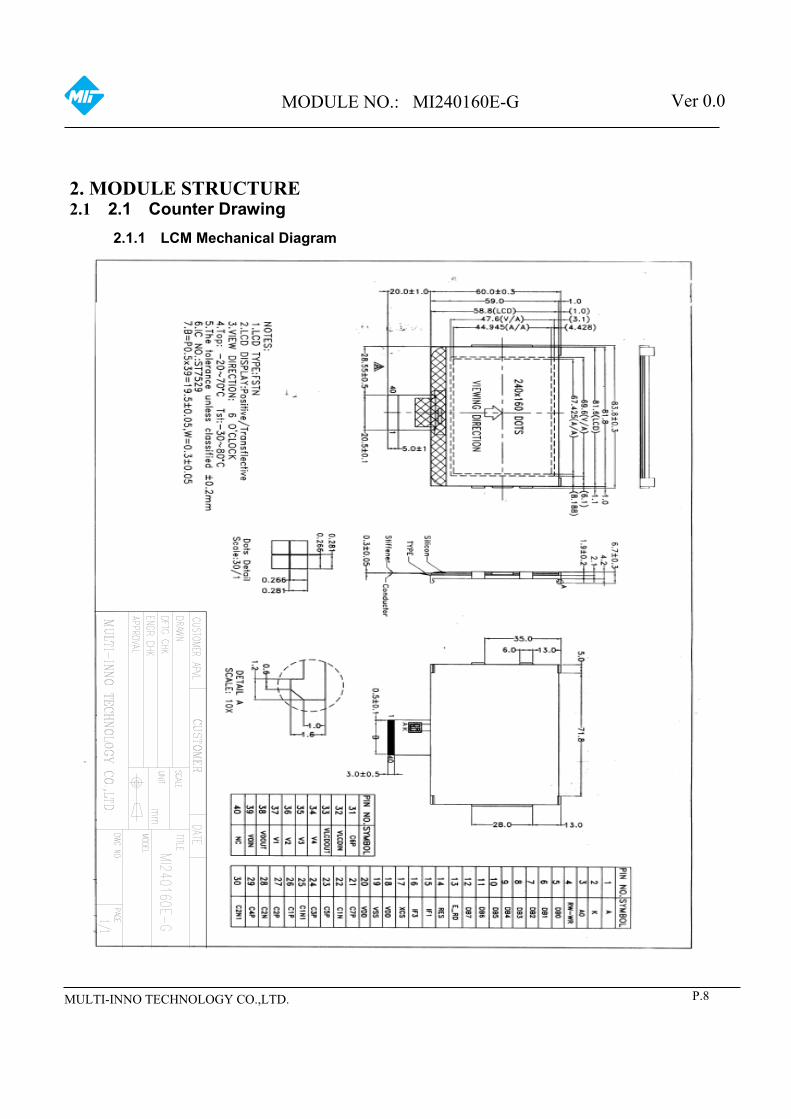
2. MODULE STRUCTURE 2.1 2.1 Counter Drawing
2.1.1 LCM Mechanical Diagram
P.8 MULTI-INNO TECHNOLOGY CO.,LTD.
MODULE NO.: MI240160E-G Ver 0.0

2.1.2 Block Diagram
P.9 MULTI-INNO TECHNOLOGY CO.,LTD.
MODULE NO.: MI240160E-G Ver 0.0

2.2Interface Pin Description
Pin No. Symbol Function 1 A Power supply for LED B/L.(Anode) 2 K Power supply for LED B/L (Cathode)
3 A0 Register select input pin -A0=”H”:DB0 to DB8 or SI are display data -A0=”L”: DB0 to DB8 or SI are control data
4 RW-WR
5~12 DB0~DB7
They connect to the standard 8-bit MPU bus via the 8 bit bi-directional bus. When the following interface is selected and the XCS pin is high, the following pins become impedance, which should be fixed to VDD or VSS.
13 E_RD
14 RES Reset input pin. When RST is “L”, initialization is executed. 15 IF1
16 IF3
17 XCS Chip select input pins Data/instruction I/O is enabled only when XCS is “L”. When chip select is non-active, DB0 to DB8 may be high impedance.
18 VDD Power supply (VDD=3.3V) 19 VSS Power supply (VSS=0) 20 VDD Power supply (VDD=3.3V)
21 C7P DC/DC voltage converter. Connect a capacitor between this terminal and the �7X VLCD; 8X C1N terminal.
P.10 MULTI-INNO TECHNOLOGY CO.,LTD.
MODULE NO.: MI240160E-G Ver 0.0

22 C1N DC/DC voltage converter. Connect a capacitor between this terminal and the �5X OPEN; 6X also C5P; 8X also C7P terminal
23 C5P DC/DC voltage converter. Connect a capacitor between this terminal and the �5X VLCD; 6X C1N terminal.
24 C3P DC/DC voltage converter. Connect a capacitor between this terminal and the �3X VLCD; 4X C1N terminal.
25 C1N1 DC/DC voltage converter. Connect a capacitor between this terminal and the C1P terminal.
26 C1P DC/DC voltage converter. Connect a capacitor between this terminal and the C1N1 terminal.
27 C2P DC/DC voltage converter. Connect a capacitor between this terminal and the 2X VLCD; 3X C2N terminal.
28 C2N DC/DC voltage converter. Connect a capacitor between this terminal and the �2X VLCD; 3X C2P terminal.
29 C4P DC/DC voltage converter. Connect a capacitor between this terminal and the �4X VLCD; 5X C2N terminal.
30 C2N1 DC/DC voltage converter. Connect a capacitor between this terminal and the �6X VLCD; 7X C6P terminal.
31 C6P DC/DC voltage converter. Connect a capacitor between this terminal and the �6X VLCD; 7X C2N1 terminal.
32 VLCDIN
An external LCD supply voltage can be supplied using the VLCDIN pad. In this case, VLCDOUT has to be left open, and the Internal voltage generator has to be programmed to zero.(SET register VB=0)
33 VLCDOUT If the internal voltage generator is used, the VLCDIN VLCDOUT
must be connected together. If an external supply is used, this pin must be left open.
34 V4 35 V3 36 V2 37 V1 38 V0OUT
39 V0IN
P.11 MULTI-INNO TECHNOLOGY CO.,LTD.
MODULE NO.: MI240160E-G Ver 0.0

40 NC Not connection 2.3 Timing Characteristics
P.12 MULTI-INNO TECHNOLOGY CO.,LTD.
MODULE NO.: MI240160E-G Ver 0.0
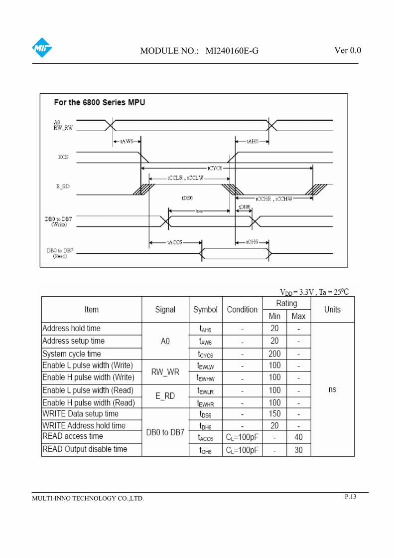
P.13 MULTI-INNO TECHNOLOGY CO.,LTD.
MODULE NO.: MI240160E-G Ver 0.0
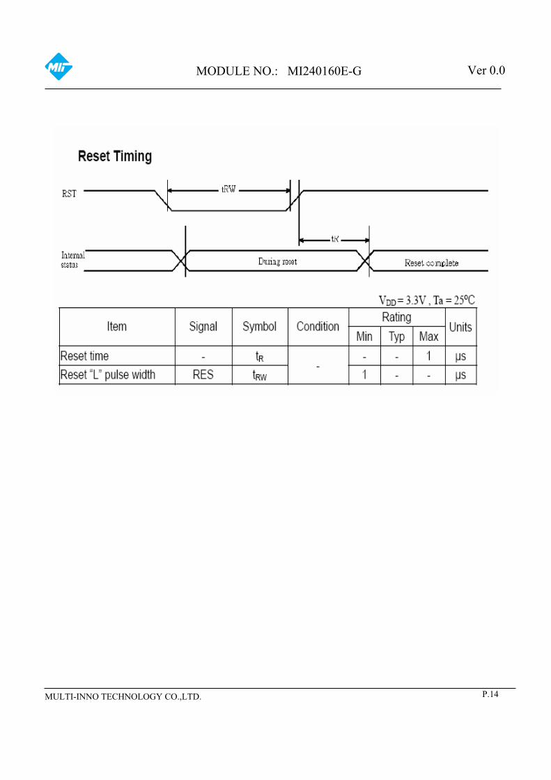
P.14 MULTI-INNO TECHNOLOGY CO.,LTD.
MODULE NO.: MI240160E-G Ver 0.0
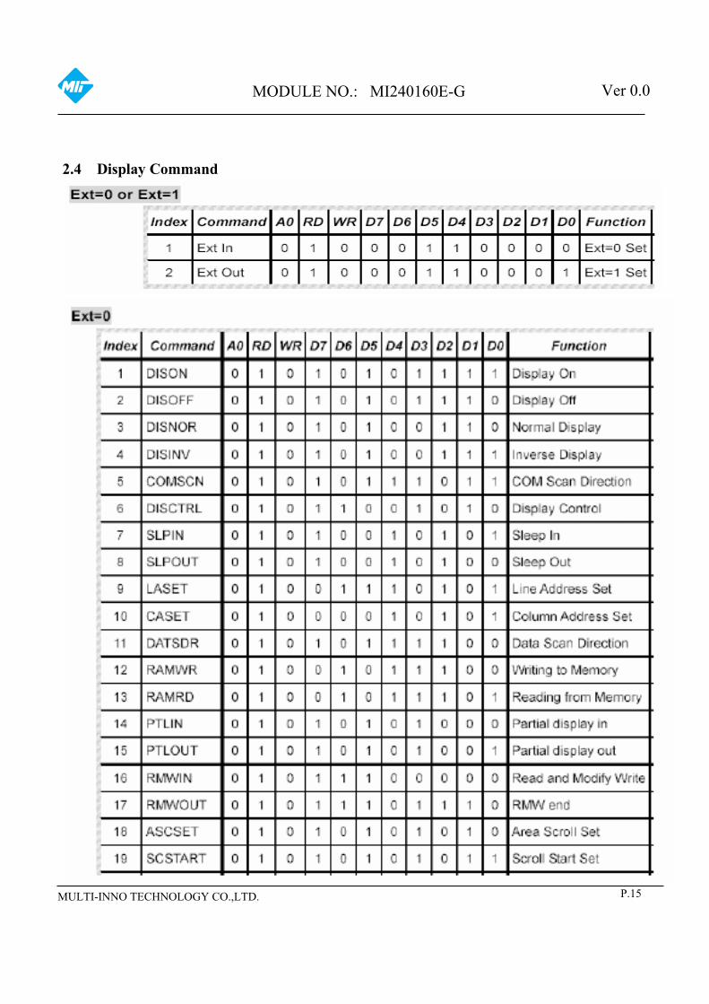
2.4 Display Command
P.15 MULTI-INNO TECHNOLOGY CO.,LTD.
MODULE NO.: MI240160E-G Ver 0.0

P.16 MULTI-INNO TECHNOLOGY CO.,LTD.
MODULE NO.: MI240160E-G Ver 0.0

3. QUALITY ASSURANCE SYSTEM
3.1 Quality Assurance Flow Chart
Item Customer Sales R&D Q.A Manufactur
ing Product control
Purchase Inventory
control
Marketing &
Design
Sample Approval
Pilot Run &
Mass Product
Ship Out
OK
Request
Info Survey
Inquiry Project evaluation
Project Validation
Quote OK NG
Contract
Design check
Sample test
Verification
Sample approval
NG
NG
Pilot run & Reliability test
Verification
Specification preparation OK
Mass production
Inspection NG OK
Shipment
NG
Ship out
OK
P.17 MULTI-INNO TECHNOLOGY CO.,LTD.
MODULE NO.: MI240160E-G Ver 0.0

Item Customer Sales R&D Q.A Manufactu
ring Product control
Purchase Inventory
control
Sales Service
Q.A Activity
1. ISO 9001 Maintenance Activities 2. Process improvement proposal 3. Equipment calibration 4. Education And Training Activities 5. Standardization Management
Info Claim
Failure analysis
Corrective action
Tracking
Analysis report
P.18 MULTI-INNO TECHNOLOGY CO.,LTD.
MODULE NO.: MI240160E-G Ver 0.0

3.2 Inspection Specification �Inspection Standard : MIL-STD-105E Table Normal Inspection Single Sampling Level � . �Equipment : Gauge MIL-STD Tester Sample�Defect Level : Major Defect AQL 0.4; Minor Defect AQL 1.5 .
�OUT Going Defect Level : Sampling . �Manner of appearance test : (1). The test be under 40W×2 fluorescent light ’ and distance of view must be at 30 cm. (2). The test direction is base on about around 45� of vertical line. (Fig. 1) (3). Definition of area . (Fig. 2)
� Specification: NO Item Criterion level
1.1 The part number is inconsistent with work order of Production.
Major
1.2 Mixed production types. Major
01
Product condition 1.3 Assembled in inverse direction. Major
02 Quantity 2.1 The quantity is inconsistent with work order of production. Major
03 Outline dimension 3.1 Product dimension and structure must conform to
Structure diagram. Major
4.1 Missing line character dot and icon. Major 4.2 No function or no display. Major 4.3 Output data is error. Major 4.4 LCD viewing angle defect. Major
04
Electrical Testing
4.5 Current consumption exceeds product specifications. Major
05
Black or white
dot scratch contamination Round type
5.1 Round type: 5.1.1 display only : �White and black spots on display � 0.30mm, no more than Four white or black spots present. �Densely spaced : NO more than two spots or lines within 3mm
Minor
P.19 MULTI-INNO TECHNOLOGY CO.,LTD.
MODULE NO.: MI240160E-G Ver 0.0
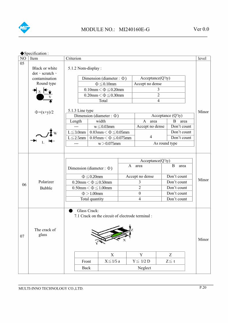
�Specification : NO Item Criterion level 05
Black or white dot scratch contamination Round type
�=(x+y)/2
5.1.2 Nom-display :
Dimension (diameter : �) Acceptance(Q’ty) ��0.10mm Accept no dense
0.10mm���0.20mm 3 0.20mm���0.30mm 2
Total 4 5.1.3 Line type
Dimension (diameter : �) Acceptance (Q’ty) Length width A area B area
--- w�0.03mm Accept no dense Don’t count L�3.0mm 0.03mm���0.05mm Don’t count L�2.5mm 0.05mm���0.075mm
4 Don’t count
--- w�0.075mm As round type
Minor
06
Polarizer Bubble
Acceptance(Q’ty)
Dimension (diameter : �) A area B area
��0.20mm Accept no dense Don’t count 0.20mm���0.50mm 3 Don’t count 0.50mm���1.00mm 2 Don’t count
��1.00mm 0 Don’t count Total quantity 4 Don’t count
Minor
07
The crack of glass
� Glass Crack: 7.1 Crack on the circuit of electrode terminal :
X Y Z Front X�1/5 a Y� 1/2 D Z� t Back Neglect
Minor
P.20 MULTI-INNO TECHNOLOGY CO.,LTD.
MODULE NO.: MI240160E-G Ver 0.0

�Specification : NO Item Criterion Level
� Glass Crack:
7.2 General glass crack and corner edge: 7.2.1
X Y Z Neglect Out A area Neglect
X Y Z Neglect Out A area Neglect
Minor
07
The crack of glass
X: The length of Crack
Y: The width of
crack
Z: The thickness of crack
D: terminal length
T: The thickness of
glass
A : The length of glass
7.3 Glass remain:
X Y Neglect � 1/3 d
Minor
P.21 MULTI-INNO TECHNOLOGY CO.,LTD.
MODULE NO.: MI240160E-G Ver 0.0

�Specification : NO Item Criterion Level 07
The crack of glass
X: The length of Crack
Y: The width of
crack
Z: The thickness of crack
D: terminal length
T: The thickness of
glass
A : The length of glass
7.4 Corner crack and medial crack:
X Y Z �1/5a Crack can’t enter viewing area �1/2t
�1/5a Crack can’t exceed the half of
width of SP width of SP 1/2t<Z�2t
Minor
8.1 Backlight can’t work normally. Major
8.2 Backlight doesn’t light or color is wrong. Major
08
Backlight elements
8.3 Illumination source flickers when lit. Major
9.1 pin type must match type in specification sheet Major
9.2 No short circuits in components on PCB or FPC Major
9.3Product packaging must the same as specified on
packaging specification sheet.
Major
9.4 The folding and peeled off in polarizer are not
acceptable
Major
09
General appearance
9.5 The PCB or FPC between B/L assembled distance
(PCB or FPC) is �1.5mm
Major
P.22 MULTI-INNO TECHNOLOGY CO.,LTD.
MODULE NO.: MI240160E-G Ver 0.0

4. RELIABILITY TEST 4.1 Reliability Test Condition NO. TEST ITEM TEST CONDITION
1 High Temperature Storage Test Keep in 80 �2� 96 hrs Surrounding temperature, then storage at normal condition 4hrs
2 Low Temperature Storage Test Keep in -30 �2� 96 hrs Surrounding temperature, then storage at normal condition 4hrs
3
High Humidity Storage
Keep in +60�/90%RH duration for 96 hrs Surrounding temperature, then storage at normal condition 4hrs (Excluding the polarizer)Or Keep in +40�/90%RH duration for 96 hrs Surrounding temperature, then storage at normal condition 4hrs Air Discharge: Apply 6 KV with 5 times Discharge for each polarity +/-
Contact Discharge: Apply 250V with 5 times discharge for each polarity +/-
4
ESD Test
1. Temperature ambient:15��35� 2. Humidity relative:30%�60% 3. Energy Storage Capacitance(Cs+Cd):150pF�10% 4. Discharge Resistance(Rd):330��10% 5. Discharge, mode of operation: Single Discharge (time between successive discharges at least 1 s) (Tolerance lf the output voltage indication: �5%)
5
Temperature Cycling Test
-20� � 25� � 70� � 25� (30mins) (5mins) (30mins) (5mins)
10 Cycle Surrounding temperature, then storage at normal condition 4hrs
6
Vibration Test (Packaged)
1. Sine wave 10�55HZ frequency (1 min) 2. The amplitude of vibration :1.5 mm 3. Each direction (XYZ) duration for 2 Hrs
7
Drop Test (Packaged)
Drop direction :�3 comer /1 edges /6 sides etch 1times
Packing Weight (Kg) Drop Height (cm) 0 ~ 45.4 122
45.4 ~ 90.8 76 90.8 ~ 454 61 Over 454 46
P.23 MULTI-INNO TECHNOLOGY CO.,LTD.
MODULE NO.: MI240160E-G Ver 0.0

5. PRECAUTION RELATING PRODUCT HANDLING 5.1 SAFETY
5.1.1 If the LCD panel breaks , be careful not to get the liquid crystal to touch your skin. 5.1.2 If the liquid crystal touches your skin or clothes , please wash it off immediately by
using soap and water. 5.2 HANDLING
5.2.1 Avoid any strong mechanical shock which can break the glass. 5.2.2 Avoid static electricity which can damage the CMOS LSI—When working with the
module , be sure to ground your body and any electrical equipment you may be using. 5.2.3 Do not remove the panel or frame from the module.
5.2.4 The polarizing plate of the display is very fragile. So , please handle it very carefully ,do not touch , push or rub the exposed polarizing with anything harder than an HB pencil lead (glass , tweezers , etc.)
5.2.5 Do not wipe the polarizing plate with a dry cloth , as it may easily scratch the surface of plate.
5.2.6 Do not touch the display area with bare hands , this will stain the display area. 5.2.7 Do not use ketonics solvent & aromatic solvent. Use with a soft cloth soaked with
a cleaning naphtha solvent. 5.2.8 To control temperature and time of soldering is 350�20�and 3-5 sec. 5.2.9 To avoid liquid (include organic solvent) stained on LCM .
5.3 STORAGE 5.3.1 Store the panel or module in a dark place where the temperature is 25� �5�
and the humidity is below 65% RH. 5.3.2 Do not place the module near organics solvents or corrosive gases.
5.3.3 Do not crush , shake , or jolt the module. 5.4 TERMS OF WARRANTY
5.4.1 Applicable warrant period The period is within thirteen months since the date of shipping out under normal using and storage conditions.
5.4.2 Unaccepted responsibility This product has been manufactured to your company’s specification as a part for use in your company’s general electronic products. It is guaranteed to perform according to delivery specifications. For any other use apart from general electronic equipment , we cannot take responsibility if the product is used in nuclear power control equipment , aerospace equipment , fire and security systems or any other applications in which there is a direct risk to human life and where extremely high levels of reliability are required
P.24 MULTI-INNO TECHNOLOGY CO.,LTD.
MODULE NO.: MI240160E-G Ver 0.0
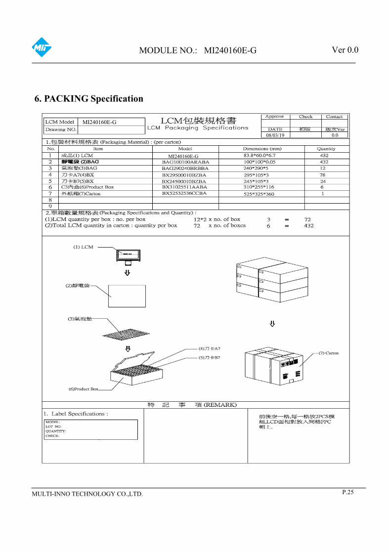
6. PACKING Specification
P.25 MULTI-INNO TECHNOLOGY CO.,LTD.
MODULE NO.: MI240160E-G Ver 0.0
MI240160E-G
0.008/03/19
MI240160E-G