product specification - emc.com.t · 6.1.23 bank 2 r7 adoc ... vi product specification (v1.3)...
TRANSCRIPT

EM78F562N/F662N
8-Bit Microcontroller
Product Specification
DOC. VERSION 1.3
ELAN MICROELECTRONICS CORP.
April 2016
Trademark Acknowledgments: IBM is a registered trademark and PS/2 is a trademark of IBM. Windows is a trademark of Microsoft Corporation.
ELAN and ELAN logo are trademarks of ELAN Microelectronics Corporation.
Copyright © 2016 by ELAN Microelectronics Corporation All Rights Reserved Printed in Taiwan The contents of this specification are subject to change without further notice. ELAN Microelectronics assumes no
responsibility concerning the accuracy, adequacy, or completeness of this specification. ELAN Microelectronics
makes no commitment to update, or to keep current the information and material contained in this specification.
Such information and material may change to conform to each confirmed order.
In no event shall ELAN Microelectronics be made responsible for any claims attributed to errors, omissions, or
other inaccuracies in the information or material contained in this specification. ELAN Microelectronics shall not
be liable for direct, indirect, special incidental, or consequential damages arising from the use of such information
or material.
The software (if any) described in this specification is furnished under a license or nondisclosure agreement, and
may be used or copied only in accordance with the terms of such agreement.
ELAN Microelectronics products are not intended for use in life support appliances, devices, or systems. Use of
ELAN Microelectronics product in such applications is not supported and is prohibited.
NO PART OF THIS SPECIFICATION MAY BE REPRODUCED OR TRANSMITTED IN ANY FORM OR BY
ANY MEANS WITHOUT THE EXPRESSED WRITTEN PERMISSION OF ELAN MICROELECTRONICS.
ELAN MICROELECTRONICS CORPORATION
Headquarters:
No. 12, Innovation Road 1
Hsinchu Science Park
Hsinchu, TAIWAN 308
Tel: +886 3 563-9977
Fax: +886 3 563-9966
http://www.emc.com.tw
Hong Kong:
Elan (HK) Microelectronics
Corporation, Ltd.
Flat A, 19F., World Tech Centre
95 How Ming Street, Kwun Tong
Kowloon, HONG KONG
Tel: +852 2723-3376
Fax: +852 2723-7780
USA:
Elan Information
Technology Group (U.S.A.)
PO Box 601
Cupertino, CA 95015
U.S.A.
Tel: +1 408 366-8225
Fax: +1 408 366-8225
Shenzhen:
Elan Microelectronics
Shenzhen, Ltd.
8A Floor, Microprofit Building
Gaoxin South Road 6
Shenzhen Hi-Tech Industrial Park
South Area, Shenzhen
CHINA 518057
Tel: +86 755 2601-0565
Fax: +86 755 2601-0500
Shanghai:
Elan Microelectronics
Shanghai, Ltd.
6F, Ke Yuan Building
No. 5 Bibo Road
Zhangjiang Hi-Tech Park
Shanghai, CHINA 201203
Tel: +86 21 5080-3866
Fax: +86 21 5080-0273
Contents
Product Specification (V1.3) 04.07.2016 iii
Contents
1 General Description ................................................................................................ 1
2 Features ................................................................................................................... 1
3 Pin Assignment ....................................................................................................... 2
4 Pin Description ........................................................................................................ 4
4.1 EM78F562N/F662N .......................................................................................... 4 5 Block Diagram ......................................................................................................... 6
6 Functional Description ............................................................................................ 7
6.1 Operational Registers ....................................................................................... 7 6.1.1 R0 (Indirect Addressing Register) ....................................................................... 7 6.1.2 R1 (Timer Clock/Counter) ................................................................................... 7 6.1.3 R2 (Program Counter) and Stack ....................................................................... 7 6.1.4 R3 (Status Register) ......................................................................................... 10 6.1.5 R4 (RAM Select Register) ................................................................................ 10 6.1.6 Bank 0 R5 ~ R8 (Port 5 ~ Port 8) ..................................................................... 10 6.1.7 Bank 0 R9 TBPTL (Low Byte of Table Pointer Register) .................................. 10 6.1.8 Bank 0 RA (Wake-up Control Register) ............................................................ 10 6.1.9 Bank 0 RB (EEPROM Control Register) .......................................................... 11 6.1.10 Bank 0 RC (128 Bytes EEPROM Address) ...................................................... 12 6.1.11 Bank 0 RD (128 Bytes EEPROM Data) ............................................................ 12 6.1.12 Bank 0 RE (CPU Operating Control Register) .................................................. 12 6.1.13 Bank 0 RF (Interrupt Status Register) .............................................................. 13 6.1.14 R10 ~ R3F ........................................................................................................ 14 6.1.15 Bank 1 R5 ~R7 ................................................................................................. 14 6.1.16 Bank 1 R8 TC2CR (Timer 2 Control) ................................................................ 14 6.1.17 Bank 1 R9 TC2DH (Timer 2 High Byte Data Buffer) ......................................... 17 6.1.18 Bank 1 RA TC2DL (Timer 2 Low Byte Data Buffer) .......................................... 17 6.1.19 Bank 1 RB ~RE ................................................................................................. 17 6.1.20 Bank 1 RF (Interrupt Status Register) .............................................................. 17 6.1.21 Bank 2 R5 AISR (ADC Input Select Register) .................................................. 18 6.1.22 Bank 2 R6 ADCON (A/D Control Register) ....................................................... 19 6.1.23 Bank 2 R7 ADOC (A/D Offset Calibration Register) ......................................... 20 6.1.24 Bank 2 R8 ADDH (AD High 8-Bit Data Buffer) ................................................. 20 6.1.25 Bank 2 R9 ADDL (AD Low 2-Bit Data Buffer) ................................................... 20 6.1.26 Bank 2 RA, RC ~ RE ........................................................................................ 20 6.1.27 Bank 2 RB CMPCON (Comparator Control Register) ...................................... 21 6.1.28 Bank 2 RF (Pull-high Control Register 1) ......................................................... 22 6.1.29 Bank 3 R5 ......................................................................................................... 22 6.1.30 Bank 3 R6 TBPTH (High Byte of Table Pointer Register)................................. 22 6.1.31 Bank 3 R7~RC .................................................................................................. 22 6.1.32 Bank 3 RD TC3CR (Timer 3 Control) ............................................................... 22 6.1.33 Bank 3 RE TC3D (Timer 3 Data Buffer)............................................................ 25 6.1.34 Bank 3 RF (Pull-down Control Register 1) ....................................................... 25
6.2 Special Function Registers ............................................................................. 25 6.2.1 A (Accumulator) ................................................................................................ 25 6.2.2 CONT (Control Register) .................................................................................. 25 6.2.3 IOC5 ~ IOC8 (I/O Port Control Register) .......................................................... 26 6.2.4 IOC9 .................................................................................................................. 26

Contents
iv Product Specification (V1.3) 04.07.2016
6.2.5 IOCA (WDT Control Register) ........................................................................... 26 6.2.6 IOCB (Pull-down Control Register 2) ................................................................ 27 6.2.7 IOCC (Open-drain Control Register) ................................................................ 28 6.2.8 IOCD (Pull-high Control Register 2) ................................................................. 28 6.2.9 IOCE (Interrupt Mask Register 2) ..................................................................... 28 6.2.10 IOCF (Interrupt Mask Register 1) ..................................................................... 29
6.3 TCC/WDT and Prescaler ................................................................................ 30 6.4 I/O Ports ......................................................................................................... 31 6.5 Reset and Wake-up ........................................................................................ 34
6.5.1 Reset ................................................................................................................. 34 6.5.2 Wake-up ............................................................................................................ 37 6.5.3 Summary of Register Initial Values after Reset ................................................ 38 6.5.4 Status of RST, T, and P of the Status Register ................................................. 42
6.6 Interrupt .......................................................................................................... 43 6.7 Data EEPROM (only for EM78F662N) ............................................................ 45
6.7.1 Data EEPROM Control Register....................................................................... 45 6.7.1.1 RB (EEPROM Control Register) ........................................................ 45 6.7.1.2 RC (128 Bytes EEPROM Address) ................................................... 46 6.7.1.3 RD (256 Bytes EEPROM Data) ......................................................... 46
6.7.2 Programming Step / Example Demonstration .................................................. 46 6.7.2.1 Programming Step ............................................................................. 46 6.7.2.2 Example Demonstration Programs .................................................... 46
6.8 Analog-to-Digital Converter (ADC) .................................................................. 47 6.8.1 ADC Control Register (AISR/R5, ADCON/R6, ADOC/R7) ............................... 48
6.8.1.1 Bank 2 R5 AISR (ADC Input Select Register) ................................... 48 6.8.1.2 Bank 2 R6 ADCON (A/D Control Register) ........................................ 49 6.8.1.3 Bank 2 R7 ADOC (A/D Offset Calibration Register) .......................... 50
6.8.2 ADC Data Buffer (ADDH, ADDL/R8, R9) .......................................................... 50 6.8.3 A/D Sampling Time ........................................................................................... 50 6.8.4 A/D Conversion Time ........................................................................................ 51 6.8.5 A/D Operation during Sleep Mode .................................................................... 51 6.8.6 Programming Steps/Considerations ................................................................. 52
6.8.6.1 Programming Steps ........................................................................... 52 6.8.6.2 Demonstration Programs ................................................................... 52
6.9 Timer/Counter 2 .............................................................................................. 54 6.10 Timer/Counter 3 .............................................................................................. 56 6.11 Comparator ..................................................................................................... 57
6.11.1 Comparator Outputs ......................................................................................... 58 6.11.2 Comparator Interrupt ........................................................................................ 58 6.11.3 Wake-up from Sleep Mode ............................................................................... 58
6.12 Oscillator ......................................................................................................... 59 6.12.1 Oscillator Modes ............................................................................................... 59 6.12.2 Crystal Oscillator/Ceramic Resonators (Crystal) .............................................. 60 6.12.3 External RC Oscillator Mode ............................................................................ 61 6.12.4 Internal RC Oscillator Mode .............................................................................. 63
6.13 Code Option Register ..................................................................................... 63 6.13.1 Code Option Register (Word 0) ........................................................................ 63 6.13.2 Code Option Register (Word 1) ........................................................................ 64 6.13.3 Customer ID Register (Word 2) ........................................................................ 65
6.14 Power-on Considerations ................................................................................ 66 6.15 External Power-on Reset Circuit ..................................................................... 66 6.16 Residue-Voltage Protection ............................................................................. 67 6.17 Instruction Set ................................................................................................. 68

Contents
Product Specification (V1.3) 04.07.2016 v
7 Timing Diagrams ................................................................................................... 71
8 Absolute Maximum Ratings .................................................................................. 72
9 DC Electrical Characteristics ................................................................................ 72
9.1 Data EEPROM Electrical Characteristics ........................................................ 73 9.2 Program Flash Memory Electrical Characteristics ........................................... 74 9.3 A/D Converter Characteristics ......................................................................... 74 9.4 Comparator Characteristics ............................................................................ 75
10 AC Electrical Characteristics ................................................................................ 75
APPENDIX
A Ordering and Manufacturing Information ............................................................ 76
B Package Type ......................................................................................................... 77
C Package Information ............................................................................................. 78
C.1 EM78F562N/F662ND16 300mil ...................................................................... 78 C.2 EM78F562N/F662NSO16 300mil ................................................................... 79 C.3 EM78F662NQN16A 4x4mm ............................................................................ 80 C.4 EM78F662NSS16 150mil ............................................................................... 81 C.5 EM78F562N/F662ND18 300mil ...................................................................... 82 C.6 EM78F562N/F662NSO18 300mil ................................................................... 83 C.7 EM78F562N/F662ND20 300mil ...................................................................... 84 C.8 EM78F562/F662NSO20 300mil ...................................................................... 85
D Quality Assurance and Reliability ........................................................................ 86
D.1 Address Trap Detect ....................................................................................... 86
Contents
vi Product Specification (V1.3) 04.07.2016
Specification Revision History
Doc. Version Revision Description Date
1.0 Initial release version 2010/04/29
1.1
1. Modified the ICC1 and ICC2 current
2. Deleted the QFN16 package of EM78F562N.
3. Modified the EM78F662NQN16 to EM78F662NQN16A.
4. Fixed the Code Option Word 2 Bit 7 to “1”
2012/06/29
1.2
1. Added LVR characteristics in the DC Electrical
Characteristics section.
2. Added SSOP package for EM78F662N.
2013/05/29
1.3
1. Added power consumption for EEPROM
2. Modified the EEPROM Endurance cycle from 100K to
1000K.
3. Added Apendix A for Ordering and Manufacturing
Information
2016/04/07
EM78F562N/F662N
8-Bit Microcontroller
Product Specification (V1.3) 04.07.2016 1 (This specification is subject to change without prior notice)
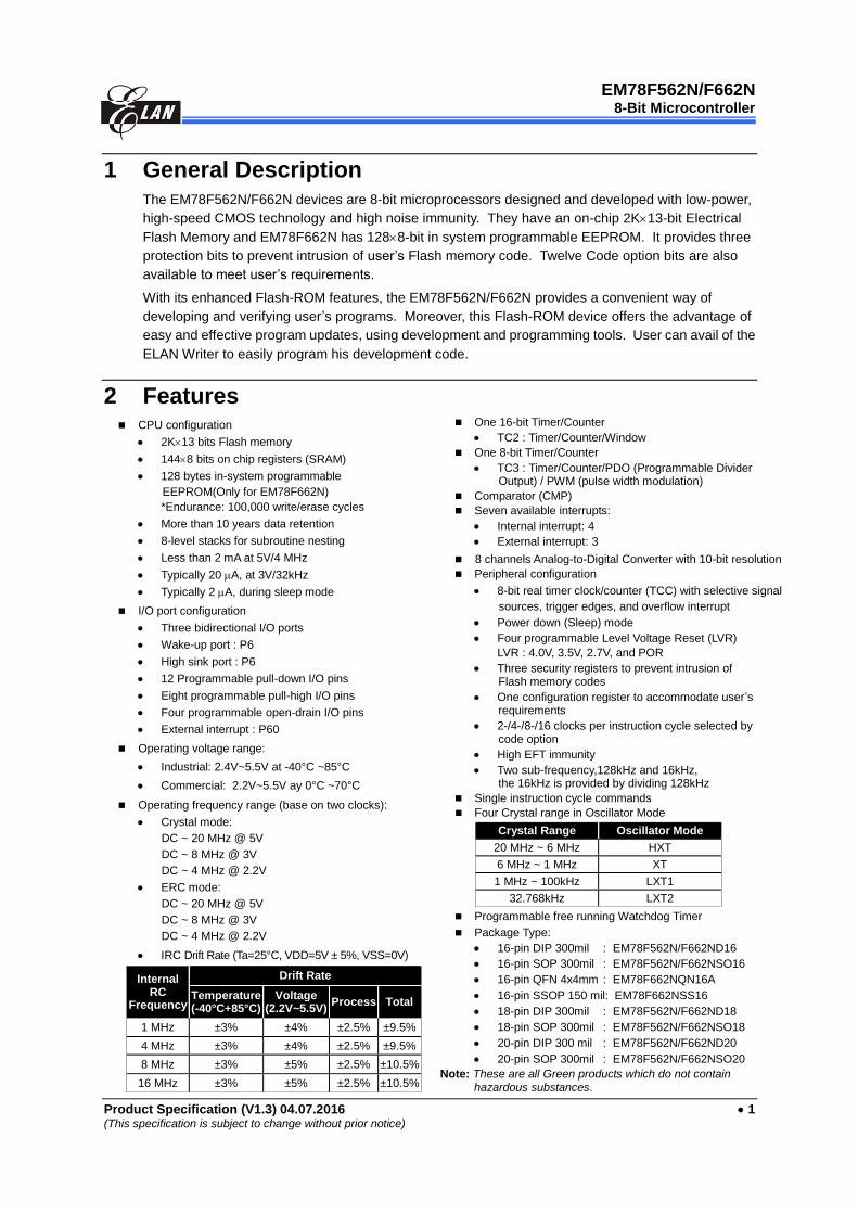
1 General Description The EM78F562N/F662N devices are 8-bit microprocessors designed and developed with low-power,
high-speed CMOS technology and high noise immunity. They have an on-chip 2K13-bit Electrical
Flash Memory and EM78F662N has 1288-bit in system programmable EEPROM. It provides three
protection bits to prevent intrusion of user’s Flash memory code. Twelve Code option bits are also
available to meet user’s requirements.
With its enhanced Flash-ROM features, the EM78F562N/F662N provides a convenient way of
developing and verifying user’s programs. Moreover, this Flash-ROM device offers the advantage of
easy and effective program updates, using development and programming tools. User can avail of the
ELAN Writer to easily program his development code.
2 Features CPU configuration
2K13 bits Flash memory
1448 bits on chip registers (SRAM)
128 bytes in-system programmable
EEPROM(Only for EM78F662N)
*Endurance: 100,000 write/erase cycles
More than 10 years data retention
8-level stacks for subroutine nesting
Less than 2 mA at 5V/4 MHz
Typically 20 A, at 3V/32kHz
Typically 2 A, during sleep mode
I/O port configuration
Three bidirectional I/O ports
Wake-up port : P6
High sink port : P6
12 Programmable pull-down I/O pins
Eight programmable pull-high I/O pins
Four programmable open-drain I/O pins
External interrupt : P60
Operating voltage range:
Industrial: 2.4V~5.5V at -40°C ~85°C
Commercial: 2.2V~5.5V ay 0°C ~70°C
Operating frequency range (base on two clocks):
Crystal mode:
DC ~ 20 MHz @ 5V
DC ~ 8 MHz @ 3V
DC ~ 4 MHz @ 2.2V
ERC mode:
DC ~ 20 MHz @ 5V
DC ~ 8 MHz @ 3V
DC ~ 4 MHz @ 2.2V
IRC Drift Rate (Ta=25°C, VDD=5V ± 5%, VSS=0V)
Internal RC
Frequency
Drift Rate
Temperature (-40°C+85°C)
Voltage (2.2V~5.5V)
Process Total
1 MHz ±3% ±4% ±2.5% ±9.5%
4 MHz ±3% ±4% ±2.5% ±9.5%
8 MHz ±3% ±5% ±2.5% ±10.5%
16 MHz ±3% ±5% ±2.5% ±10.5%
One 16-bit Timer/Counter
TC2 : Timer/Counter/Window
One 8-bit Timer/Counter
TC3 : Timer/Counter/PDO (Programmable Divider Output) / PWM (pulse width modulation)
Comparator (CMP)
Seven available interrupts:
Internal interrupt: 4
External interrupt: 3
8 channels Analog-to-Digital Converter with 10-bit resolution
Peripheral configuration
8-bit real timer clock/counter (TCC) with selective signal
sources, trigger edges, and overflow interrupt
Power down (Sleep) mode
Four programmable Level Voltage Reset (LVR)
LVR : 4.0V, 3.5V, 2.7V, and POR
Three security registers to prevent intrusion of Flash memory codes
One configuration register to accommodate user’s requirements
2-/4-/8-/16 clocks per instruction cycle selected by code option
High EFT immunity
Two sub-frequency,128kHz and 16kHz, the 16kHz is provided by dividing 128kHz
Single instruction cycle commands
Four Crystal range in Oscillator Mode
Crystal Range Oscillator Mode
20 MHz ~ 6 MHz HXT
6 MHz ~ 1 MHz XT
1 MHz ~ 100kHz LXT1
32.768kHz LXT2
Programmable free running Watchdog Timer
Package Type:
16-pin DIP 300mil : EM78F562N/F662ND16
16-pin SOP 300mil : EM78F562N/F662NSO16
16-pin QFN 4x4mm : EM78F662NQN16A
16-pin SSOP 150 mil: EM78F662NSS16
18-pin DIP 300mil : EM78F562N/F662ND18
18-pin SOP 300mil : EM78F562N/F662NSO18
20-pin DIP 300 mil : EM78F562N/F662ND20
20-pin SOP 300mil : EM78F562N/F662NSO20
Note: These are all Green products which do not contain hazardous substances.

EM78F562N/F662N
8-Bit Microcontroller
2 Product Specification (V1.3) 04.07.2016
(This specification is subject to change without prior notice)
3 Pin Assignment
EM
78
F5
62
N/F
66
2N
-16
Pin
1
2
3
4
5
6
7
8 9
10
16
15
14
13
12
11
P72
P51
VDD (VDD)
P70 (DATA)
P50/VREF
P71 (CLK)
P54/OSCI/RCOUT
P55/OSCO/ERCin
VSS (VSS)
P60/AD0//INT/CMPOUT
P52
P77/TCC/AD5
P61/AD1/CMP+
P53
P62/AD2/CMP-
P83//RESET (RESET)
EM
78
F5
62
N/F
66
2N
-18
Pin
1
2
3
4
5
6
7
8
9 10
18
17
16
15
14
13
12
11
P73/AD4
P54/OSCI/RCOUT
P72
P51
VDD (VDD)
P70 (DATA)
P50/VREF
P55/OSCO/ERCin
P71 (CLK)
P63/AD3
VSS (VSS)
P60/AD0//INT/CMPOUT
P52
P77/TCC/AD5
P61/AD1/CMP+
P53
P62/AD2/CMP-
P83//RESET (RESET)
Figure 3-1 EM78F562N/F662ND16/SO16 Figure 3-2 EM78F562/F662ND18/SO18
E
M7
8F
56
2N
/F6
62
N-2
0P
in
1
2
3
4
5
6
7
8
9
10
20
19
18
17
16
15
14
13
12
11
P56/TC2/AD6
P63/AD3
VSS (VSS)
P60/AD0//INT/CMPOUT
P52
P77/TCC/AD5
P61/AD1/CMP+
P53
P62/AD2/CMP-
P83//RESET (RESET)
P57/TC3/PDO/AD7
P73/AD4
P72
P51
VDD (VDD)
P70 (DATA)
P50/VREF
P71 (CLK)
P54/OSCI/RCOUT
P55/OSCO/ERCin
5
8
3 4
6
7
9101112
13
14
15
16
EM78F662N-
QFN16
1 2
VS
S (V
SS
)
P8
3//R
ES
ET
(/RE
SE
T)
P7
7/T
CC
/AD
6
P6
0/A
D1//IN
T/C
MP
OU
T
P5
5/O
SC
O/E
RC
in
P5
4/O
SC
I/RC
OU
T
VD
D (V
DD
)
P7
0 (D
AT
A)
P61/AD1/CMP+
P62/AD2/CMP-
P72
P71 (CLK)
P53
P52
P51
P50/VREF
Figure 3-3 EM78F562/F662ND20/SO20 Figure 3-4 EM78F662NQN16A
EM78F562N/F662N
8-Bit Microcontroller
Product Specification (V1.3) 04.07.2016 3 (This specification is subject to change without prior notice)
EM
78
F6
62
N-S
SO
P1
6
1
2
3
4
5
6
7
8 9
10
16
15
14
13
12
11
P72
P51
VDD (VDD)
P70 (DATA)
P50/VREF
P71 (CLK)
P54/OSCI/RCOUT
P55/OSCO/ERCin
VSS (VSS)P60/AD0//INT/CMPOUT
P53
P77/TCC/AD5
P61/AD1/CMP+
P52
P62/AD2/CMP-
P83//RESET (RESET)
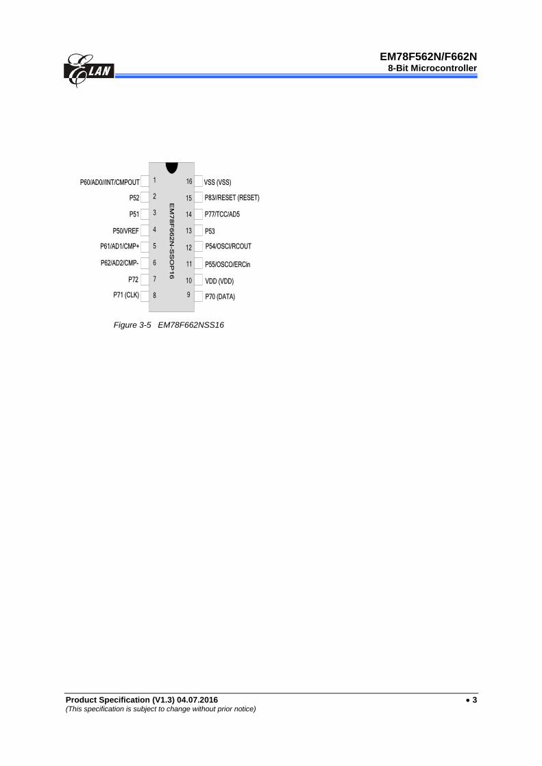
Figure 3-5 EM78F662NSS16

EM78F562N/F662N
8-Bit Microcontroller
4 Product Specification (V1.3) 04.07.2016
(This specification is subject to change without prior notice)
4 Pin Description
4.1 EM78F562N/F662N
Legend: ST: Schmitt Trigger input AN: analog pin
CMOS: CMOS output XTAL: Oscillation pin for crystal / resonator
Name Function Input Type
Output Type
Description
P50/VREF P50 ST CMOS Bidirectional I/O pin with programmable pull-down
VREF AN ADC external voltage reference
P51 P51 ST CMOS Bidirectional I/O pin with programmable pull-down
P52 P52 ST CMOS Bidirectional I/O pin with programmable pull-down
P53 P53 ST CMOS Bidirectional I/O pin with programmable pull-down
P54/OSCI/RCOUT
P54 ST CMOS Bidirectional I/O pin
OSCI XTAL Clock input of crystal/resonator oscillator
RCOUT CMOS Clock output of internal RC oscillator
Clock output of external RC oscillator (open-drain)
P55/OSCO/ERCin
P55 ST CMOS Bidirectional I/O pin
OSCO XTAL Clock output of crystal/resonator oscillator
ERCin AN External RC input pin
P56/TC2/AD6
P56 ST CMOS Bidirectional I/O pin
TC2 ST Timer 2 clock input
AD6 AN ADC Input 6
P57/TC3/PDO/AD7
P57 ST CMOS Bidirectional I/O pin
TC3 ST Timer 3 clock input
PDO CMOS Programmable divider output
AD7 AN ADC Input 7
P60/AD0//INT/CMPOUT
P60 ST CMOS Bidirectional I/O pin with programmable pull-down, pull-high, open-drain, and pin change wake-up
AD0 AN ADC Input 0
/INT ST External interrupt pin
CMPOUT CMOS Comparator output
P61/AD1/CMP+
P61 ST CMOS Bidirectional I/O pin with programmable pull-down, pull-high, open-drain, and pin change wake-up
AD1 AN ADC Input 1
CMP+ AN Non-inverting end of comparator
EM78F562N/F662N
8-Bit Microcontroller
Product Specification (V1.3) 04.07.2016 5 (This specification is subject to change without prior notice)
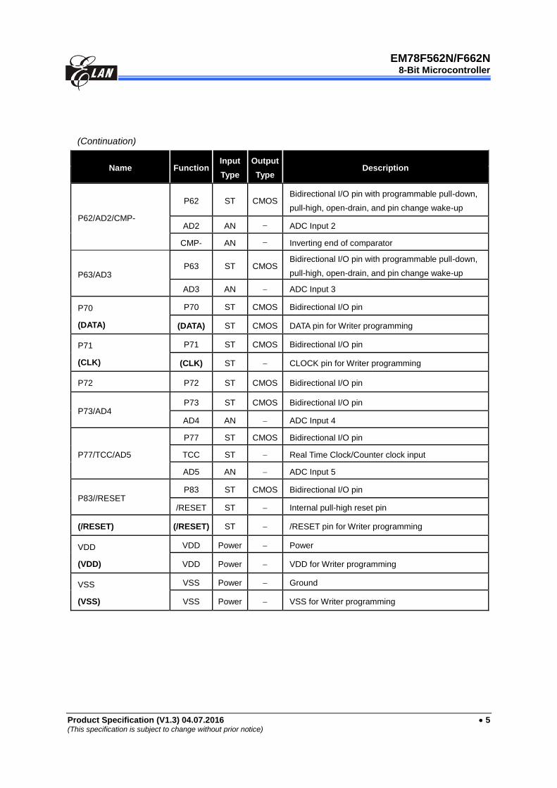
(Continuation)
Name Function Input
Type
Output
Type Description
P62/AD2/CMP-
P62 ST CMOS Bidirectional I/O pin with programmable pull-down,
pull-high, open-drain, and pin change wake-up
AD2 AN ADC Input 2
CMP- AN Inverting end of comparator
P63/AD3 P63 ST CMOS
Bidirectional I/O pin with programmable pull-down,
pull-high, open-drain, and pin change wake-up
AD3 AN ADC Input 3
P70
(DATA)
P70 ST CMOS Bidirectional I/O pin
(DATA) ST CMOS DATA pin for Writer programming
P71
(CLK)
P71 ST CMOS Bidirectional I/O pin
(CLK) ST CLOCK pin for Writer programming
P72 P72 ST CMOS Bidirectional I/O pin
P73/AD4 P73 ST CMOS Bidirectional I/O pin
AD4 AN ADC Input 4
P77/TCC/AD5
P77 ST CMOS Bidirectional I/O pin
TCC ST Real Time Clock/Counter clock input
AD5 AN ADC Input 5
P83//RESET P83 ST CMOS Bidirectional I/O pin
/RESET ST Internal pull-high reset pin
(/RESET) (/RESET) ST /RESET pin for Writer programming
VDD
(VDD)
VDD Power Power
VDD Power VDD for Writer programming
VSS
(VSS)
VSS Power Ground
VSS Power VSS for Writer programming

EM78F562N/F662N
8-Bit Microcontroller
6 Product Specification (V1.3) 04.07.2016
(This specification is subject to change without prior notice)
5 Block Diagram
Flash
ROM
R3(Status Reg.)
ACC
InstructionDecoder
Instruction
Register
ALU
PC
Interrupt
Circuit
8-level stack
(13-bit)
Interrupt
Control
Register
Oscillation
Generator
RAM
Mux
Crystal
R4
Ext.RC
IntRC
WDT
TCC
LVR
TCC
P5
P50
P57P56P55P54P53P52P51
Ext INT
Reset
P6
P60
P63P62P61
EEPROM*
P7
P70
P73P72P71
ADC 10 bits Comparator
ADin (0~7) CMP+, CMP-, CMPOUT
TC 2
16 bit
TC 3
8-bit
PWM
PDO
TC 2
TC 3P77
P83
P8
*Only for EM78F662N
Figure 5-1 Functional Block Diagram
EM78F562N/F662N
8-Bit Microcontroller
Product Specification (V1.3) 04.07.2016 7 (This specification is subject to change without prior notice)
6 Functional Description
6.1 Operational Registers
6.1.1 R0 (Indirect Addressing Register)
R0 is not a physically implemented register. It is used as an indirect addressing
pointer. Any instruction using R0 as a pointer actually accesses data pointed by the
RAM Select Register (R4).
6.1.2 R1 (Timer Clock/Counter)
R1 is incremented by an external signal edge, which is defined by TE bit (CONT-4)
through the TCC pin, or by the instruction cycle clock. It is writable and readable as any
other registers. It is defined by resetting PSTE (CONT-3).
The prescaler is assigned to TCC, if the PSTE bit (CONT-3) is reset. The contents of
the prescaler counter are cleared only when the TCC register is written with a value.
6.1.3 R2 (Program Counter) and Stack
Depending on the device type, R2 and hardware stack are 10-bit wide. The structure is
depicted in Figure 6-1.
The configuration structure generates 2K13 bits on-chip Flash ROM addresses to the
relative programming instruction codes. One program page is 1024 words long.
R2 is set as all “0”s when under a reset condition.
“JMP” instruction allows direct loading of the lower 10 program counter bits. Thus,
“JMP” allows the PC to go to any location within a page (1K).
“CALL” instruction loads the lower 10 bits of the PC and PC+1 is pushed onto the stack.
Thus, the subroutine entry address can be located anywhere within a page.
“LJMP” instruction allows direct loading of the lower 11 program counter bits. Thus,
“LJMP” allows the PC to go to any location within 2K.
“LCALL” instruction loads the lower 11 bits of the PC and PC+1 is pushed onto the
stack. Thus, the subroutine entry address can be located anywhere within 2K.
“RET” (“RETL k”, “RETI”) instruction loads the program counter with the contents of the
top-level stack.

EM78F562N/F662N
8-Bit Microcontroller
8 Product Specification (V1.3) 04.07.2016
(This specification is subject to change without prior notice)
“ADD R2, A” allows a relative address to be added to the current PC, and the ninth and
above bits of the PC will be incremented progressively.
“MOV R2, A” allows to load an address from the “A” register to the lower 8 bits of the
PC, and the ninth and tenth bits of the PC remain unchanged.
Any instruction except “ADD R2,A” that is written to R2 (e.g. “MOV R2, A”, “BC R2, 6”)
will cause the ninth bit and the tenth bits (A8~A9) of the PC to remain unchanged.
All instructions are single instruction cycle (fclk/2, fclk/4, fclk/8 or fclk/16) except for
instructions that would change the contents of R2. Such instructions will need one
more instruction cycle.
A10 A9 A8 A7 ~ A0
R3 [5]
CALL
RET
RETL
RETI
00 : PAGE0 0000~03FF
01 : PAGE1 0400~07FF
PC
Stack Level 1
Stack Level 2
Stack Level 3
Stack Level 4
Stack Level 5
Reset Vector 0000h
On-chip Program Memory
Use
r Me
mo
ry S
pa
ce
Store ACC, R3, R4
External INT Pin interrupt Vector 0003h
Port 6 Pin Status Change Interrupt Vector 0006h
TCC Overflow 0009h
TC2 Interrupt Vector 0024h
TC3 Interrupt Vector 0027h
Comparator 0033h
07FFh
Stack Level 6
Stack Level 7
Stack Level 8
AD Interrupt Vector 0030h
Figure 6-1 Program Counter Organization

EM78F562N/F662N
8-Bit Microcontroller
Product Specification (V1.3) 04.07.2016 9 (This specification is subject to change without prior notice)
05
06
07
08
09
0A
0B
0C
0D
0E
0F
04
03
02
01 R1 (TCC Buffer)
R2 (PC)
R3 (STATUS)
R4 (RSR, Bank Select)
R5 (Port 5 /IO data)
R6 (Port 6 I/O data)
R5 (Reserved)
RB (Reserved)
R6 (Reserved)
R9 (AD low 2-bit
Data Buffer)
R7 (Port 7 I/O data)
R8 (Port 8 I/O data)
R9 (TBPTL)
R7 (Reserved)
RD (Timer 3 Control)
RC (Reserved)
RE (Timer 3 Data Buffer) RE (Reserved)
RD (Reserved)
RE (Reserved)
IOC6 (Port 6 I/O Control)
IOC7 (Port 7 I/O Control)
IOC8 (Port 8 I/O Control)
IOC9 (Reserved)
IOCE (Interrupt Mask
Register 2)
IOCF (Interrupt Mask
Register 1)
16-Byte Common Register
10
:
1F
Bank 0
32x8
20
:
3F
R4(7,6)
Address
Register
Bank 0
Register
Bank 1
Register
Bank 2
Control
Register
(0,1) (1,0)
Register
Bank 3
(1,1)
RA (Wake-up Control
Register)
R8 (Timer 2 Control)
R9 (Timer 2 High Byte
Data Buffer)
RA (Timer 2 Low Byte
Data Buffer)
RB (Comparator
Control Register)
RC (Reserved)
RD (Reserved)IOCD (Pull-high
Control Register 2)
IOCC (Open Drain
Control Register)
IOCB (Pull-down
Control Register 2)
R6 (ADC Control
Register)
R7 (Reserved)
R8 (AD high 8-bit
Data Buffer)
R5 (ADC Input Select
Register) IOC5 (Port 5 I/O Control)
R9 (Reserved)
RB (Reserved)
RA (Reserved)
RC (Reserved)
R5 (Reserved)
R6 (TBPTH)
R7 (Reserved)
R8 (Reserved)
RB (EEPROM Control
Register)
RC (EEPROM Address
Register)
RD (EEPROM Data
Register)
RA (Reserved)
RF (Pull-high Control
Register 1)RF (Pull-down Control
Register 1)
IOCA (WDT Control)
RE (CPU Operating
Control Register)
RF (Interrupt Flag 1) RF (Interrupt Flag 2)
Bank 0
32x8
Bank 0
32x8
Bank 0
32x8
Figure 6-2 Data Memory Configuration
EM78F562N/F662N
8-Bit Microcontroller
10 Product Specification (V1.3) 04.07.2016
(This specification is subject to change without prior notice)
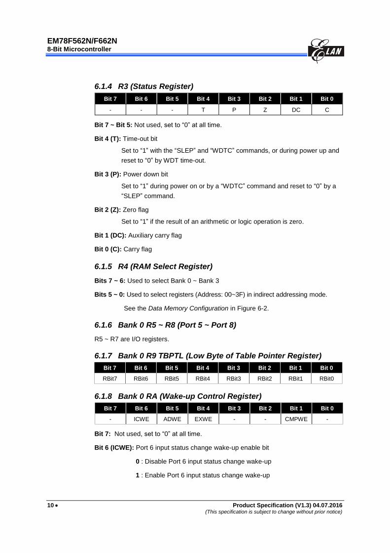
6.1.4 R3 (Status Register)
Bit 7 Bit 6 Bit 5 Bit 4 Bit 3 Bit 2 Bit 1 Bit 0
- - - T P Z DC C
Bit 7 ~ Bit 5: Not used, set to “0” at all time.
Bit 4 (T): Time-out bit
Set to “1” with the “SLEP” and “WDTC” commands, or during power up and
reset to “0” by WDT time-out.
Bit 3 (P): Power down bit
Set to “1” during power on or by a “WDTC” command and reset to “0” by a
“SLEP” command.
Bit 2 (Z): Zero flag
Set to “1” if the result of an arithmetic or logic operation is zero.
Bit 1 (DC): Auxiliary carry flag
Bit 0 (C): Carry flag
6.1.5 R4 (RAM Select Register)
Bits 7 ~ 6: Used to select Bank 0 ~ Bank 3
Bits 5 ~ 0: Used to select registers (Address: 00~3F) in indirect addressing mode.
See the Data Memory Configuration in Figure 6-2.
6.1.6 Bank 0 R5 ~ R8 (Port 5 ~ Port 8)
R5 ~ R7 are I/O registers.
6.1.7 Bank 0 R9 TBPTL (Low Byte of Table Pointer Register)
Bit 7 Bit 6 Bit 5 Bit 4 Bit 3 Bit 2 Bit 1 Bit 0
RBit7 RBit6 RBit5 RBit4 RBit3 RBit2 RBit1 RBit0
6.1.8 Bank 0 RA (Wake-up Control Register)
Bit 7 Bit 6 Bit 5 Bit 4 Bit 3 Bit 2 Bit 1 Bit 0
- ICWE ADWE EXWE - - CMPWE -
Bit 7: Not used, set to “0” at all time.
Bit 6 (ICWE): Port 6 input status change wake-up enable bit
0 : Disable Port 6 input status change wake-up
1 : Enable Port 6 input status change wake-up

EM78F562N/F662N
8-Bit Microcontroller
Product Specification (V1.3) 04.07.2016 11 (This specification is subject to change without prior notice)
Bit 5 (ADWE): ADC wake-up enable bit
0 : Disable ADC wake-up
1 : Enable ADC wake-up
When ADC completed status is used to enter an interrupt vector or to
wake-up the EM78F562N/F662N from sleep, with A/D conversion
running, the ADWE bit must be set to “Enable“.
Bit 4 (EXWE): External wake-up enable bit
0 : Disable External /INT pin wake-up
1 : Enable External /INT pin wake-up
Bit 2: Not used, set to “0” at all time
Bit 1 (CMPWE): Comparator wake-up enable bit
0 : Disable Comparator wake-up
1 : Enable Comparator wake-up
Bits 3, 0: Not used, set to “0” at all time
6.1.9 Bank 0 RB (EEPROM Control Register)
Bit 7 Bit 6 Bit 5 Bit 4 Bit 3 Bit 2 Bit 1 Bit 0
RD WR EEWE EEDF EEPC - - -
Bit 7 (RD): Read control register
0 : Does not execute EEPROM read
1 : Read EEPROM content, (RD can be set by software, and cleared by
hardware after Read instruction is completed)
Bit 6 (WR): Write control register
0 : Write cycle to the EEPROM is complete.
1 : Initiate a write cycle, (WR can be set by software, WR is cleared by
hardware after Write cycle is completed)
Bit 5 (EEWE): EEPROM Write Enable bit.
0 : Prohibit write to the EEPROM
1 : Allows EEPROM write cycles
Bit 4 (EEDF): EEPROM Detective Flag
0 : Write cycle is completed
1 : Write cycle is unfinished

EM78F562N/F662N
8-Bit Microcontroller
12 Product Specification (V1.3) 04.07.2016
(This specification is subject to change without prior notice)
Bit 3 (EEPC): EEPROM power-down control bit
0 : Switch off the EEPROM
1 : EEPROM is operating
Bits 2 ~ 0: Not used, set to “0” at all time
*This register is only for EM78F662N.
6.1.10 Bank 0 RC (128 Bytes EEPROM Address)
Bit 7 Bit 6 Bit 5 Bit 4 Bit 3 Bit 2 Bit 1 Bit 0
- EE_A6 EE_A5 EE_A4 EE_A3 EE_A2 EE_A1 EE_A0
Bits 6 ~ 0: 128 bytes EEPROM address
*This register is only for EM78F662N.
6.1.11 Bank 0 RD (128 Bytes EEPROM Data)
Bit 7 Bit 6 Bit 5 Bit 4 Bit 3 Bit 2 Bit 1 Bit 0
EE_D7 EE_D6 EE_D5 EE_D4 EE_D3 EE_D2 EE_D1 EE_D0
Bits 7 ~ 0: 128 bytes EEPROM data
*This register is only for EM78F662N.
6.1.12 Bank 0 RE (CPU Operating Control Register)
Bit 7 Bit 6 Bit 5 Bit 4 Bit 3 Bit 2 Bit 1 Bit 0
- TIMERSC CPUS IDLE- - - - -
Bit 7: Not used, set to “0” at all time
Bit 6 (TIMERSC): TCC, TC2, TC3 clock source select
0 : Fs. Fs stands for the sub frequency for WDT internal RC time base.
1 : Fm. Fm stands for the main-oscillator clock
Bit 5 (CPUS): CPU Oscillator Source Select
0 : sub-oscillator (fs)
1 : main oscillator (fosc)
When CPUS=0, the CPU oscillator selects the sub-oscillator and the
main oscillator is stopped.
Bit 4 (IDLE): Idle Mode Enable Bit. This bit will determine which mode to enter after
SLEP instruction is executed.
0 : IDLE=”0”+SLEP instruction sleep mode
1 : IDLE=”1”+SLEP instruction idle mode
EM78F562N/F662N
8-Bit Microcontroller
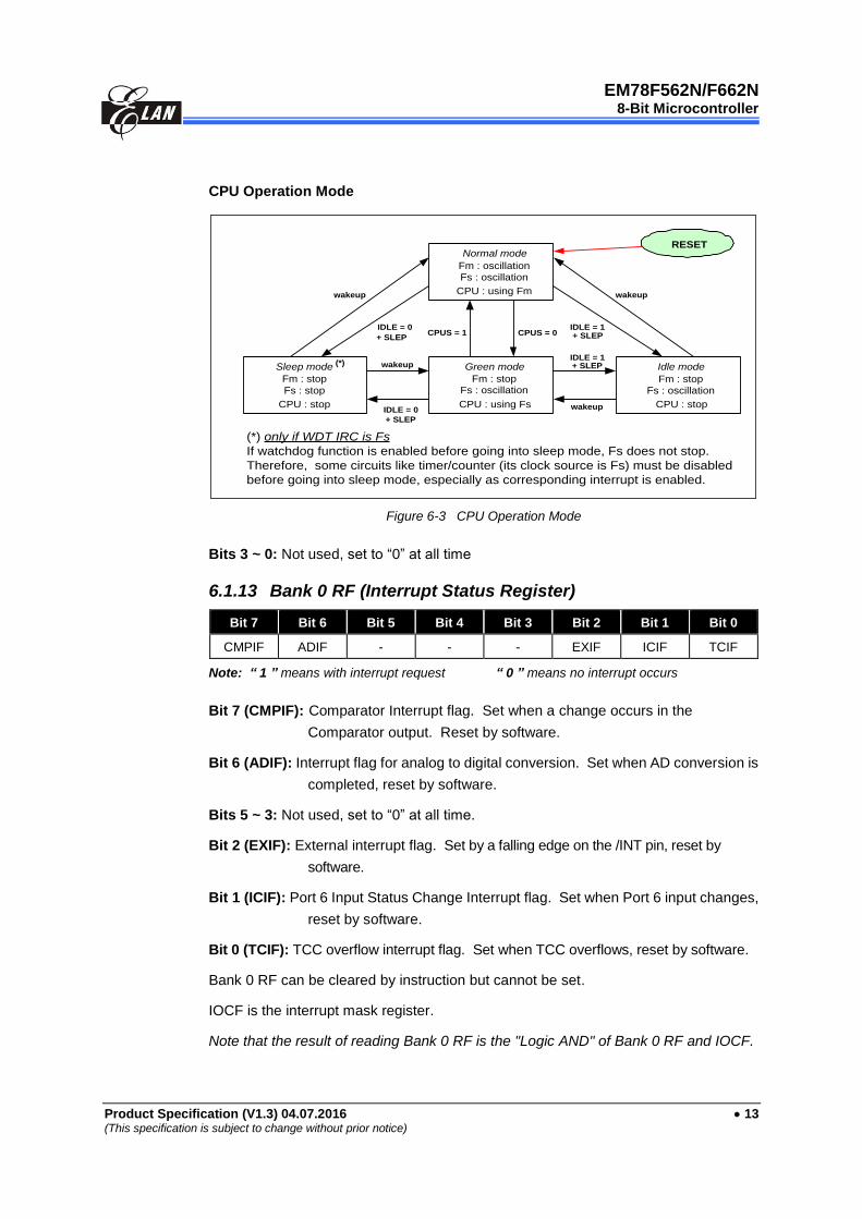
Product Specification (V1.3) 04.07.2016 13 (This specification is subject to change without prior notice)
CPU Operation Mode
Normal mode
Fm : oscillation
CPU : using Fm
Sleep mode Green mode Idle mode
CPUS = 1 CPUS = 0
wakeup
IDLE = 1
IDLE = 1
wakeup
wakeup
IDLE = 0
+ SLEP
IDLE = 0
wakeup
Fs : oscillation
Fm : stopFs : oscillation
CPU : using Fs
Fm : stopFm : stop
Fs : stop Fs : oscillation
CPU : stopCPU : stop
+ SLEP
+ SLEP+ SLEP
(*) only if WDT IRC is Fs
If watchdog function is enabled before going into sleep mode, Fs does not stop.
Therefore, some circuits like timer/counter (its clock source is Fs) must be disabled
before going into sleep mode, especially as corresponding interrupt is enabled.
(*)
RESET
Figure 6-3 CPU Operation Mode
Bits 3 ~ 0: Not used, set to “0” at all time
6.1.13 Bank 0 RF (Interrupt Status Register)
Bit 7 Bit 6 Bit 5 Bit 4 Bit 3 Bit 2 Bit 1 Bit 0
CMPIF ADIF - - - EXIF ICIF TCIF
Note: “ 1 ” means with interrupt request “ 0 ” means no interrupt occurs
Bit 7 (CMPIF): Comparator Interrupt flag. Set when a change occurs in the
Comparator output. Reset by software.
Bit 6 (ADIF): Interrupt flag for analog to digital conversion. Set when AD conversion is
completed, reset by software.
Bits 5 ~ 3: Not used, set to “0” at all time.
Bit 2 (EXIF): External interrupt flag. Set by a falling edge on the /INT pin, reset by
software.
Bit 1 (ICIF): Port 6 Input Status Change Interrupt flag. Set when Port 6 input changes,
reset by software.
Bit 0 (TCIF): TCC overflow interrupt flag. Set when TCC overflows, reset by software.
Bank 0 RF can be cleared by instruction but cannot be set.
IOCF is the interrupt mask register.
Note that the result of reading Bank 0 RF is the "Logic AND" of Bank 0 RF and IOCF.
EM78F562N/F662N
8-Bit Microcontroller
14 Product Specification (V1.3) 04.07.2016
(This specification is subject to change without prior notice)
6.1.14 R10 ~ R3F
All of these are 8-bit general-purpose registers.
6.1.15 Bank 1 R5 ~R7
These are reserved registers.
6.1.16 Bank 1 R8 TC2CR (Timer 2 Control)
Bit 7 Bit 6 Bit 5 Bit 4 Bit 3 Bit 2 Bit 1 Bit 0
RCM1 RCM0 TC2ES TC2M TC2S TC2CK2 TC2CK1 TC2CK0
Bit 7 and Bit 6 (RCM1, RCM0): IRC mode select bits
Writer Trim IRC
Bank 1 R8<7,6>
Frequency Operating Voltage
Range Stable Time
RCM1 RCM0
4 MHz
0 0 4 MHz ± 2.5% 2.2V~5.5V <5 µs
0 1 16 MHz ± 10% 4.5V~5.5V <1.5 µs
1 0 8 MHz ± 10% 3.0V~5.5V <3 µs
1 1 1 MHz ± 10% 2.2V~5.5V <22 µs
16 MHz
0 0 4 MHz ± 10% 2.2V~5.5V <6 µs
0 1 16 MHz ± 2.5% 4.5V~5.5V <1.25 µs
1 0 8 MHz ± 10% 3.0V~5.5V <3 µs
1 1 1 MHz ± 10% 2.2V~5.5V <22 µs
8 MHz
0 0 4 MHz ± 10% 2.2V~5.5V <6 µs
0 1 16 MHz ± 10% 4.5V~5.5V <1.5 µs
1 0 8 MHz ± 2.5% 3.0V~5.5V <2.5 µs
1 1 1 MHz ± 10% 2.2V~5.5V <22 µs
1 MHz
0 0 4 MHz ± 10% 2.2V~5.5V <6 µs
0 1 16 MHz ± 10% 4.5V~5.5V <1.5 µs
1 0 8 MHz ± 10% 3.0V~5.5V <3 µs
1 1 1 MHz ± 2.5% 2.2V~5.5V <20 µs
For Example:
NOTE
■ The initial values of Bank 1 R8<7, 6> will be kept the same as Word 1<3, 2>.
■ If user changes the IRC frequency from A-frequency to B-frequency, the F902N
needs to wait for some time for it to work. The waiting time corresponds to the
B-frequency.
ex : Writer trim IRC 4 MHz → Bank 1 R8<7, 6> set to “10” → holds 3 µs → F902N
works on 8 MHz ± 10%
EM78F562N/F662N
8-Bit Microcontroller
Product Specification (V1.3) 04.07.2016 15 (This specification is subject to change without prior notice)
Code Option Word 1 COBS = 0:
The initialized values of R8<7, 6> will be kept the same as Word 1<3, 2>.
The R8<7, 6> cannot change the frequency.
Code Option Word 1 COBS = 1:
The initialized values of R8<7, 6> will be kept the same as Word 1<3, 2>.
The R8<7, 6> can change, when user wants to work on other IRC frequency.
Bit 5 (TC2ES): TC2 signal edge
0 : incremented if a transition from low to high (rising edge) takes place
on the TC2 pin
1 : incremented if a transition from high to low (falling edge) takes place
on the TC2 pin
Bit 4 (TC2M): Timer/Counter 2 mode select
0 : Timer/counter mode
1 : Window mode
Bit 3 (TC2S): Timer/Counter 2 start control
0 : Stop and clear the counter
1 : Start
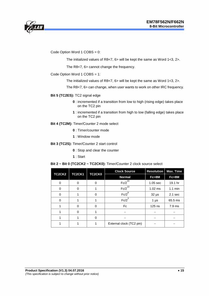
Bit 2 ~ Bit 0 (TC2CK2 ~ TC2CK0): Timer/Counter 2 clock source select
TC2CK2 TC2CK1 TC2CK0 Clock Source Resolution Max. Time
Normal Fc=8M Fc=8M
0 0 0 Fc/223
1.05 sec 19.1 hr
0 0 1 Fc/213
1.02 ms 1.1 min
0 1 0 Fc/28 32 µs 2.1 sec
0 1 1 Fc/23 1 µs 65.5 ms
1 0 0 Fc 125 ns 7.9 ms
1 0 1
1 1 0
1 1 1 External clock (TC2 pin)
EM78F562N/F662N
8-Bit Microcontroller
16 Product Specification (V1.3) 04.07.2016
(This specification is subject to change without prior notice)
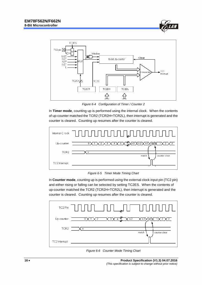
Figure 6-4 Configuration of Timer / Counter 2
In Timer mode, counting up is performed using the internal clock. When the contents
of up-counter matched the TCR2 (TCR2H+TCR2L), then interrupt is generated and the
counter is cleared. Counting up resumes after the counter is cleared.
Figure 6-5 Timer Mode Timing Chart
In Counter mode, counting up is performed using the external clock input pin (TC2 pin)
and either rising or falling can be selected by setting TC2ES. When the contents of
up-counter matched the TCR2 (TCR2H+TCR2L), then interrupt is generated and the
counter is cleared. Counting up resumes after the counter is cleared.
Figure 6-6 Counter Mode Timing Chart
EM78F562N/F662N
8-Bit Microcontroller
Product Specification (V1.3) 04.07.2016 17 (This specification is subject to change without prior notice)
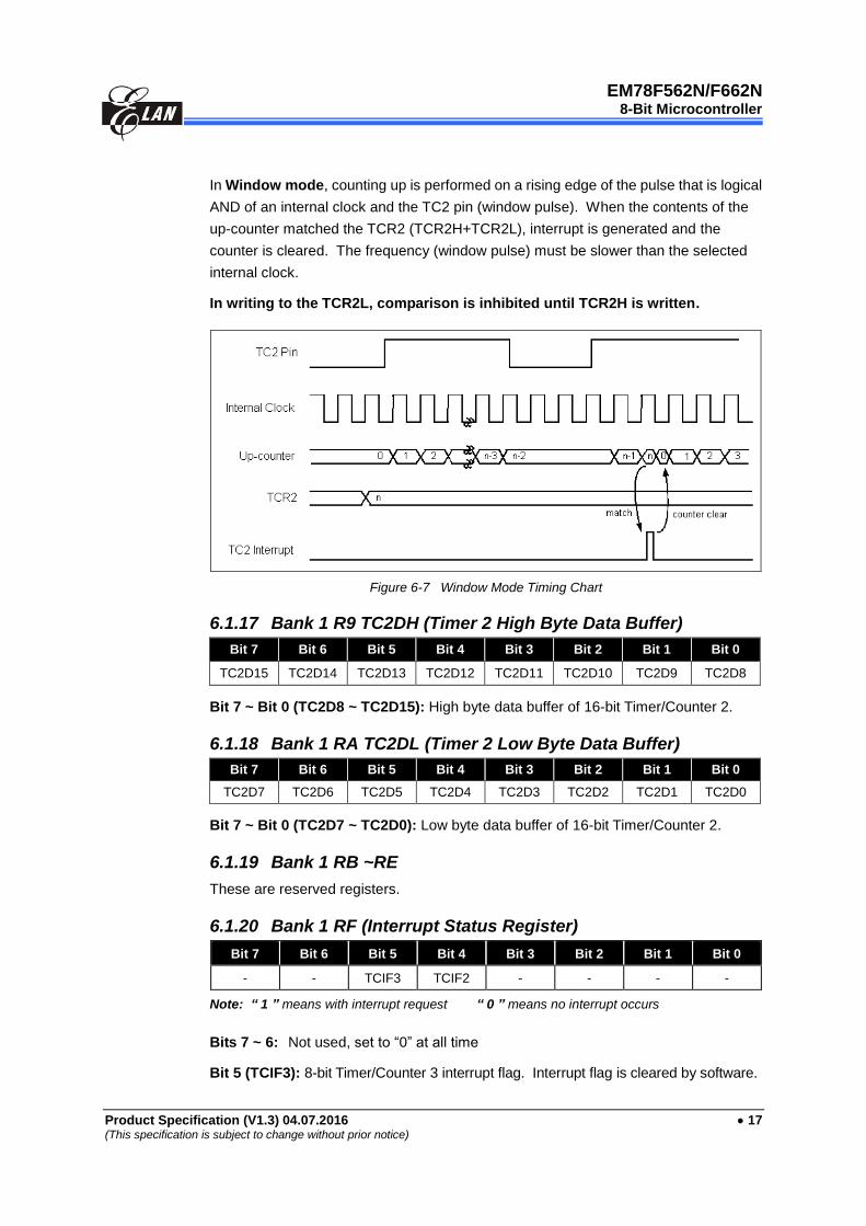
In Window mode, counting up is performed on a rising edge of the pulse that is logical
AND of an internal clock and the TC2 pin (window pulse). When the contents of the
up-counter matched the TCR2 (TCR2H+TCR2L), interrupt is generated and the
counter is cleared. The frequency (window pulse) must be slower than the selected
internal clock.
In writing to the TCR2L, comparison is inhibited until TCR2H is written.
Figure 6-7 Window Mode Timing Chart
6.1.17 Bank 1 R9 TC2DH (Timer 2 High Byte Data Buffer)
Bit 7 Bit 6 Bit 5 Bit 4 Bit 3 Bit 2 Bit 1 Bit 0
TC2D15 TC2D14 TC2D13 TC2D12 TC2D11 TC2D10 TC2D9 TC2D8
Bit 7 ~ Bit 0 (TC2D8 ~ TC2D15): High byte data buffer of 16-bit Timer/Counter 2.
6.1.18 Bank 1 RA TC2DL (Timer 2 Low Byte Data Buffer)
Bit 7 Bit 6 Bit 5 Bit 4 Bit 3 Bit 2 Bit 1 Bit 0
TC2D7 TC2D6 TC2D5 TC2D4 TC2D3 TC2D2 TC2D1 TC2D0
Bit 7 ~ Bit 0 (TC2D7 ~ TC2D0): Low byte data buffer of 16-bit Timer/Counter 2.
6.1.19 Bank 1 RB ~RE
These are reserved registers.
6.1.20 Bank 1 RF (Interrupt Status Register)
Bit 7 Bit 6 Bit 5 Bit 4 Bit 3 Bit 2 Bit 1 Bit 0
- - TCIF3 TCIF2 - - - -
Note: “ 1 ” means with interrupt request “ 0 ” means no interrupt occurs
Bits 7 ~ 6: Not used, set to “0” at all time
Bit 5 (TCIF3): 8-bit Timer/Counter 3 interrupt flag. Interrupt flag is cleared by software.

EM78F562N/F662N
8-Bit Microcontroller
18 Product Specification (V1.3) 04.07.2016
(This specification is subject to change without prior notice)
Bit 4 (TCIF2): 16-bit Timer/Counter 2 interrupt flag. Interrupt flag is cleared by software.
RF can be cleared by instruction but cannot be set.
IOCE is the interrupt mask register.
Note that the result of reading Bank 1 RF is the "logic AND" of Bank 1 RF and IOCE.
Bits 3 ~ 0: Not used, set to “0” at all time.
6.1.21 Bank 2 R5 AISR (ADC Input Select Register)
The AISR register for ADC pins as analog input or as digital I/O.
Bit 7 Bit 6 Bit 5 Bit 4 Bit 3 Bit 2 Bit 1 Bit 0
ADE7 ADE6 ADE5 ADE4 ADE3 ADE2 ADE1 ADE0
Bit 7 (ADE7): AD converter enable bit of P57 pin.
0 : Disable ADC7, P57 act as I/O pin.
1 : Enable ADC7 to act as analog input pin.
Bit 6 (ADE6): AD converter enable bit of P56 pin.
0 : Disable ADC6, P56 act as I/O pin.
1 : Enable ADC6 to act as analog input pin.
Bit 5 (ADE5): AD converter enable bit of P77 pin
0 : Disable ADC5, P77 functions as I/O pin.
1 : Enable ADC5 to function as analog input pin.
Bit 4 (ADE4): AD converter enable bit of P73 pin
0 : Disable ADC4, P73 act as I/O pin.
1 : Enable ADC4 to act as analog input pin.
Bit 3 (ADE3): AD converter enable bit of P63 pin.
0 : Disable ADC3, P63 act as I/O pin.
1 : Enable ADC3 to act as analog input pin.
Bit 2 (ADE2): AD converter enable bit of P62 pin.
0 : Disable ADC2, P62 act as I/O pin.
1 : Enable ADC2 to act as analog input pin.
Bit 1 (ADE1): AD converter enable bit of P61 pin.
0 : Disable ADC1, P61 functions as I/O pin.
1 : Enable ADC1 to function as analog input pin.
Bit 0 (ADE0): AD converter enable bit of P60 pin.
0 : Disable ADC0, P60 act as I/O pin.
1 : Enable ADC0 to act as analog input pin.
EM78F562N/F662N
8-Bit Microcontroller
Product Specification (V1.3) 04.07.2016 19 (This specification is subject to change without prior notice)
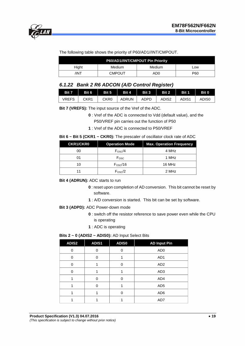
The following table shows the priority of P60/AD1//INT/CMPOUT.
P60/AD1//INT/CMPOUT Pin Priority
Hight Medium Medium Low
/INT CMPOUT AD0 P60
6.1.22 Bank 2 R6 ADCON (A/D Control Register)
Bit 7 Bit 6 Bit 5 Bit 4 Bit 3 Bit 2 Bit 1 Bit 0
VREFS CKR1 CKR0 ADRUN ADPD ADIS2 ADIS1 ADIS0
Bit 7 (VREFS): The input source of the Vref of the ADC.
0 : Vref of the ADC is connected to Vdd (default value), and the
P50/VREF pin carries out the function of P50
1 : Vref of the ADC is connected to P50/VREF
Bit 6 ~ Bit 5 (CKR1 ~ CKR0): The prescaler of oscillator clock rate of ADC
CKR1/CKR0 Operation Mode Max. Operation Frequency
00 FOSC/4 4 MHz
01 FOSC 1 MHz
10 FOSC/16 16 MHz
11 FOSC/2 2 MHz
Bit 4 (ADRUN): ADC starts to run
0 : reset upon completion of AD conversion. This bit cannot be reset by
software.
1 : A/D conversion is started. This bit can be set by software.
Bit 3 (ADPD): ADC Power-down mode
0 : switch off the resistor reference to save power even while the CPU
is operating
1 : ADC is operating
Bits 2 ~ 0 (ADIS2 ~ ADIS0): AD Input Select Bits
ADIS2 ADIS1 ADIS0 AD Input Pin
0 0 0 AD0
0 0 1 AD1
0 1 0 AD2
0 1 1 AD3
1 0 0 AD4
1 0 1 AD5
1 1 0 AD6
1 1 1 AD7

EM78F562N/F662N
8-Bit Microcontroller
20 Product Specification (V1.3) 04.07.2016
(This specification is subject to change without prior notice)
6.1.23 Bank 2 R7 ADOC (A/D Offset Calibration Register)
Bit 7 Bit 6 Bit 5 Bit 4 Bit 3 Bit 2 Bit 1 Bit 0
CALI SIGN VOF[2] VOF[1] VOF[0] - - -
Bit 7 (CALI): Calibration enable bit for A/D offset
0 : Disable calibration
1 : Enable calibration
Bit 6 (SIGN): Polarity bit of offset voltage
0 : Negative voltage
1 : Positive voltage
Bits 5 ~ 3 (VOF[2] ~ VOF[0]): Offset voltage bits
VOF[2] VOF[1] VOF[0] Offset
0 0 0 0LSB
0 0 1 1LSB
0 1 0 2LSB
0 1 1 3LSB
1 0 0 4LSB
1 0 1 5LSB
1 1 0 6LSB
1 1 1 7LSB
Bits 2 ~ 0: Not used, set to “0” at all time.
6.1.24 Bank 2 R8 ADDH (AD High 8-Bit Data Buffer)
Bit 7 Bit 6 Bit 5 Bit 4 Bit 3 Bit 2 Bit 1 Bit 0
ADD9 ADD8 ADD7 ADD6 ADD5 ADD4 ADD3 ADD2
When the A/D conversion is completed, the result of high 8-bit is loaded into the ADDH.
The ADRUN bit is cleared, and the ADIF is set. R8 is read only.
6.1.25 Bank 2 R9 ADDL (AD Low 2-Bit Data Buffer)
Bit 7 Bit 6 Bit 5 Bit 4 Bit 3 Bit 2 Bit 1 Bit 0
- - - - - - ADD1 ADD0
Bits 7 ~ 2: Not used, set to “0” at all time.
6.1.26 Bank 2 RA, RC ~ RE
These are reserved registers.

EM78F562N/F662N
8-Bit Microcontroller
Product Specification (V1.3) 04.07.2016 21 (This specification is subject to change without prior notice)
6.1.27 Bank 2 RB CMPCON (Comparator Control Register)
Bit 7 Bit 6 Bit 5 Bit 4 Bit 3 Bit 2 Bit 1 Bit 0
- - - - - CPOUT CPS1 CPS0
Bits 7 ~ 3: Not used. Set to “0” at all time.
Bit 2 (CPOUT): Result of the Comparator output
NOTE
The P60/AD1/INT/CMPOUT pin priority is as follows:
Bit 1 ~ Bit 0 (CPS1 ~ CPS0): Comparator Select bits
CO3S1 CO3S0 Function Description
0 0 Comparator is not used. P60 functions as normal I/O pin.
0 1 Used as Comparator and P60 functions as normal I/O pin.
1 0 Used as Comparator and P60 funcions as Comparator output pin
(CMPOUT)
1 1 Reserved
NOTE
The P61/AD1/CMP+ pin priority is as follows:
NOTE
The P62/AD2/CMP- pin priority is as follows:
Priority
High Medium Medium Low
INT CMPOUT AD0 P60
Priority
High Medium Low
CMP+ AD1 P61
Priority
High Medium Low
CMP- AD2 P62

EM78F562N/F662N
8-Bit Microcontroller
22 Product Specification (V1.3) 04.07.2016
(This specification is subject to change without prior notice)
6.1.28 Bank 2 RF (Pull-high Control Register 1)
Bit 7 Bit 6 Bit 5 Bit 4 Bit 3 Bit 2 Bit 1 Bit 0
- - - - /PH73 /PH72 /PH71 /PH70
Bits 7 ~ 4: Not used, set to “0” at all time.
Bit 3 (/PH73): Control bit used to enable pull-high of the P73 pin.
0 : Enable internal pull-high
1 : Disable internal pull-high
Bit 2 (/PH72): Control bit used to enable pull-high of the P72 pin.
Bit 1 (/PH71): Control bit used to enable pull-high of the P71 pin.
Bit 0 (/PH70): Control bit used to enable pull-high of the P70 pin.
The RF Register is both readable and writable.
6.1.29 Bank 3 R5
Reserved Register
6.1.30 Bank 3 R6 TBPTH (High Byte of Table Pointer Register)
Bit 7 Bit 6 Bit 5 Bit 4 Bit 3 Bit 2 Bit 1 Bit 0
MLB - - - - RBit10 RBit9 RBit8
Bit 7 (MLB): Take MSB or LSB at machine code.
Bits 6 ~ 3: No used. Set to “0” at all time.
Bits 2 ~ 0: Table point Address Bits 10 ~ 8.
6.1.31 Bank 3 R7~RC
Reserved Registers
6.1.32 Bank 3 RD TC3CR (Timer 3 Control)
Bit 7 Bit 6 Bit 5 Bit 4 Bit 3 Bit 2 Bit 1 Bit 0
TC3FF1 TC3FF0 TC3S TC3CK2 TC3CK1 TC3CK0 TC3M1 TC3M0
Bit 7 ~ Bit 6 (TC3FF1 ~ TC3FF0): Timer/Counter 3 flip-flop control
TC3FF1 TC3FF0 Operating Mode
0 0 Clear
0 1 Toggle
1 0 Set
1 1 Reserved

EM78F562N/F662N
8-Bit Microcontroller
Product Specification (V1.3) 04.07.2016 23 (This specification is subject to change without prior notice)
Bit 5 (TC3S): Timer/Counter 3 start control
0 : Stop and clear the counter
1 : Start
Bit 4 ~ Bit 2 (TC3CK2 ~ TC3CK0): Timer/Counter 3 clock source select
TC3CK2 TC3CK1 TC3CK0 Clock Source Resolution Max. Time
Normal Fc=8M Fc=8M
0 0 0 Fc/211
250 µs 64 ms
0 0 1 Fc/27 16 µs 4 ms
0 1 0 Fc/25 4 µs 1 ms
0 1 1 Fc/23 1 µs 255 µs
1 0 0 Fc/22 500 ns 127.5 µs
1 0 1 Fc/21 250 ns 63.8 µs
1 1 0 Fc 125 ns 31.9 µs
1 1 1 External clock (TC3 pin) - -
Bit 1 ~ Bit 0 (TC3M1 ~ TC3M0): Timer/Counter 3 operating mode select
TC3M1 TC3M0 Operating Mode
0 0 Timer/Counter
0 1 Reserved
1 0 Programmable Divider output
1 1 Pulse Width Modulation output
Figure 6-8 Timer / Counter 3 Configuration
In Timer Mode, counting up is performed using internal clock (rising edge trigger).
When the contents of the up-counter match the TCR3, interrupt is generated and the
counter is cleared. Counting up resumes after the counter is cleared.

EM78F562N/F662N
8-Bit Microcontroller
24 Product Specification (V1.3) 04.07.2016
(This specification is subject to change without prior notice)
In Counter Mode, counting up is performed using external clock input pin (TC3 pin).
When the contents of the up-counter match the TCR3, then interrupt is generated and
the counter is cleared. Counting up resumes after the counter is cleared.
In Programmable Divider Output (PDO) Mode, counting up is performed using the
internal clock. The contents of TCR3 are compared with the contents of the
up-counter. The F/F output is toggled and the counter is cleared each time a match is
found. The F/F output is inverted and output to /PDO pin. This mode can generate
50% duty pulse output. The F/F can be initialized by the program and it is initialized to
“0” during reset. A TC3 interrupt is generated each time the /PDO output is toggled.
0 1 3 n-1 n 0 n-1 n 0 1 n-1 0 1 2
Clock Source
Up-counter
TCR3
TC3 Interrupt
n
2 1 n
F/F
/PDO Pin
Figure 6-9 PDO Mode Timing Chart
In Pulse Width Modulation (PWM) Output mode, counting up is performed using
internal clock. The contents of TCR3 are compared with the contents of the
up-counter. The F/F is toggled when a match is found. The counter continues
counting, the F/F is toggled again when the counter overflows, after which the counter
is cleared. The F/F output is inverted and output to /PWM pin. A TC3 interrupt is
generated each time an overflow occurs. TCR3 is configured as a 2-stage shift register
and, during output, will not switch until one output cycle is completed even if TCR3 is
overwritten. Therefore, the output can be changed continuously. Also, the first time,
TRC3 is shifted by setting TC3S to “1” after data is loaded to TCR3.
0 1 n-1 n n+1 FE FF 0 n+1 FE FF 0
Clock Source
Up-counter
TCR3
TC3 Interrupt
n/n
n+2
F/F
/PWM
match overflow
n-1 n
match
n+2
overflow
1 period
n/m m/m
overwriteShift
m-11 m
Figure 6-10 PWM Mode Timing Chart
EM78F562N/F662N
8-Bit Microcontroller
Product Specification (V1.3) 04.07.2016 25 (This specification is subject to change without prior notice)
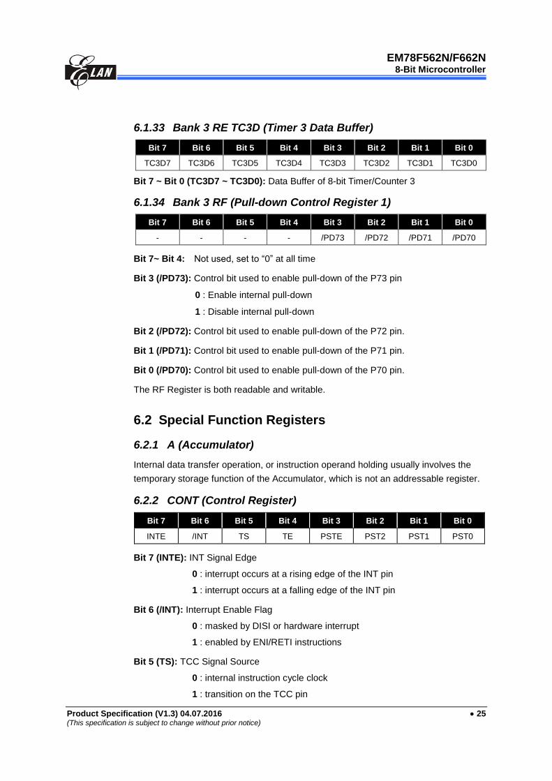
6.1.33 Bank 3 RE TC3D (Timer 3 Data Buffer)
Bit 7 Bit 6 Bit 5 Bit 4 Bit 3 Bit 2 Bit 1 Bit 0
TC3D7 TC3D6 TC3D5 TC3D4 TC3D3 TC3D2 TC3D1 TC3D0
Bit 7 ~ Bit 0 (TC3D7 ~ TC3D0): Data Buffer of 8-bit Timer/Counter 3
6.1.34 Bank 3 RF (Pull-down Control Register 1)
Bit 7 Bit 6 Bit 5 Bit 4 Bit 3 Bit 2 Bit 1 Bit 0
- - - - /PD73 /PD72 /PD71 /PD70
Bit 7~ Bit 4: Not used, set to “0” at all time
Bit 3 (/PD73): Control bit used to enable pull-down of the P73 pin
0 : Enable internal pull-down
1 : Disable internal pull-down
Bit 2 (/PD72): Control bit used to enable pull-down of the P72 pin.
Bit 1 (/PD71): Control bit used to enable pull-down of the P71 pin.
Bit 0 (/PD70): Control bit used to enable pull-down of the P70 pin.
The RF Register is both readable and writable.
6.2 Special Function Registers
6.2.1 A (Accumulator)
Internal data transfer operation, or instruction operand holding usually involves the
temporary storage function of the Accumulator, which is not an addressable register.
6.2.2 CONT (Control Register)
Bit 7 Bit 6 Bit 5 Bit 4 Bit 3 Bit 2 Bit 1 Bit 0
INTE /INT TS TE PSTE PST2 PST1 PST0
Bit 7 (INTE): INT Signal Edge
0 : interrupt occurs at a rising edge of the INT pin
1 : interrupt occurs at a falling edge of the INT pin
Bit 6 (/INT): Interrupt Enable Flag
0 : masked by DISI or hardware interrupt
1 : enabled by ENI/RETI instructions
Bit 5 (TS): TCC Signal Source
0 : internal instruction cycle clock
1 : transition on the TCC pin

EM78F562N/F662N
8-Bit Microcontroller
26 Product Specification (V1.3) 04.07.2016
(This specification is subject to change without prior notice)
Bit 4 (TE): TCC Signal Edge
0 : increment if a transition from low to high takes place on TCC pin
1 : increment if a transition from high to low takes place on TCC pin
Bit 3 (PSTE): Prescaler Enable bit for TCC
0 : prescaler disable bit, TCC rate is 1:1
1 : prescaler enable bit, TCC rate is set at Bit 2 ~ Bit 0
Bit 2 ~ Bit 0 (PST 2 ~ PST0): TCC prescaler bits
PST2 PST1 PST0 TCC Rate
0 0 0 1:2
0 0 1 1:4
0 1 0 1:8
0 1 1 1:16
1 0 0 1:32
1 0 1 1:64
1 1 0 1:128
1 1 1 1:256
CONT register is both readable and writable.
6.2.3 IOC5 ~ IOC8 (I/O Port Control Register)
A value of "1" sets the relative I/O pin into high impedance, while "0" defines the relative
I/O pin as output.
IOC5, IOC6 IOC7 and IOC8 registers are both readable and writable.
6.2.4 IOC9
Reserved registers
6.2.5 IOCA (WDT Control Register)
Bit 7 Bit 6 Bit 5 Bit 4 Bit 3 Bit 2 Bit 1 Bit 0
WDTE EIS - - PSWE PSW2 PSW1 PSW0
Bit 7 (WDTE): Control bit used to enable the Watchdog timer
0 : Disable WDT
1 : Enable WDT
WDTE is both readable and writable.
Bit 6 (EIS): Control bit used to define the function of P60 (/INT) pin
0 : P60, bidirectional I/O pin
1 : /INT, external interrupt pin. In this case, the I/O control bit of P60
(Bit 0 of IOC6) must be set to "1".

EM78F562N/F662N
8-Bit Microcontroller
Product Specification (V1.3) 04.07.2016 27 (This specification is subject to change without prior notice)
When EIS is "0", the path of /INT is masked. When EIS is "1", the status
of /INT pin can also be read by way of reading Port 6 (R6).
EIS is both readable and writable.
Bits 5 ~ 4: Not used, set to “0” at all time
Bit 3 (PSWE): Prescaler Enable bit for WDT
0 : prescaler disable bit, WDT rate is 1:1
1 : prescaler enable bit, WDT rate is set as Bit 0~Bit 2
Bit 2 ~ Bit 0 (PSW2 ~ PSW0): WDT prescaler bits
PSW2 PSW1 PSW0 WDT Rate
0 0 0 1:2
0 0 1 1:4
0 1 0 1:8
0 1 1 1:16
1 0 0 1:32
1 0 1 1:64
1 1 0 1:128
1 1 1 1:256
6.2.6 IOCB (Pull-down Control Register 2)
Bit 7 Bit 6 Bit 5 Bit 4 Bit 3 Bit 2 Bit 1 Bit 0
/PD7 /PD6 /PD5 /PD4 /PD3 /PD2 /PD1 /PD0
Bit 7 (/PD7): Control bit used to enable pull-down of the P63 pin.
0 : Enable internal pull-down
1 : Disable internal pull-down
Bit 6 (/PD6): Control bit used to enable pull-down of the P62 pin.
Bit 5 (/PD5): Control bit used to enable pull-down of the P61 pin.
Bit 4 (/PD4): Control bit used to enable pull-down of the P60 pin.
Bit 3 (/PD3): Control bit used to enable pull-down of the P53 pin.
Bit 2 (/PD2): Control bit used to enable pull-down of the P52 pin.
Bit 1 (/PD1): Control bit used to enable pull-down of the P51 pin.
Bit 0 (/PD0): Control bit used to enable pull-down of the P50 pin.
The IOCB Register is both readable and writable.
EM78F562N/F662N
8-Bit Microcontroller
28 Product Specification (V1.3) 04.07.2016
(This specification is subject to change without prior notice)
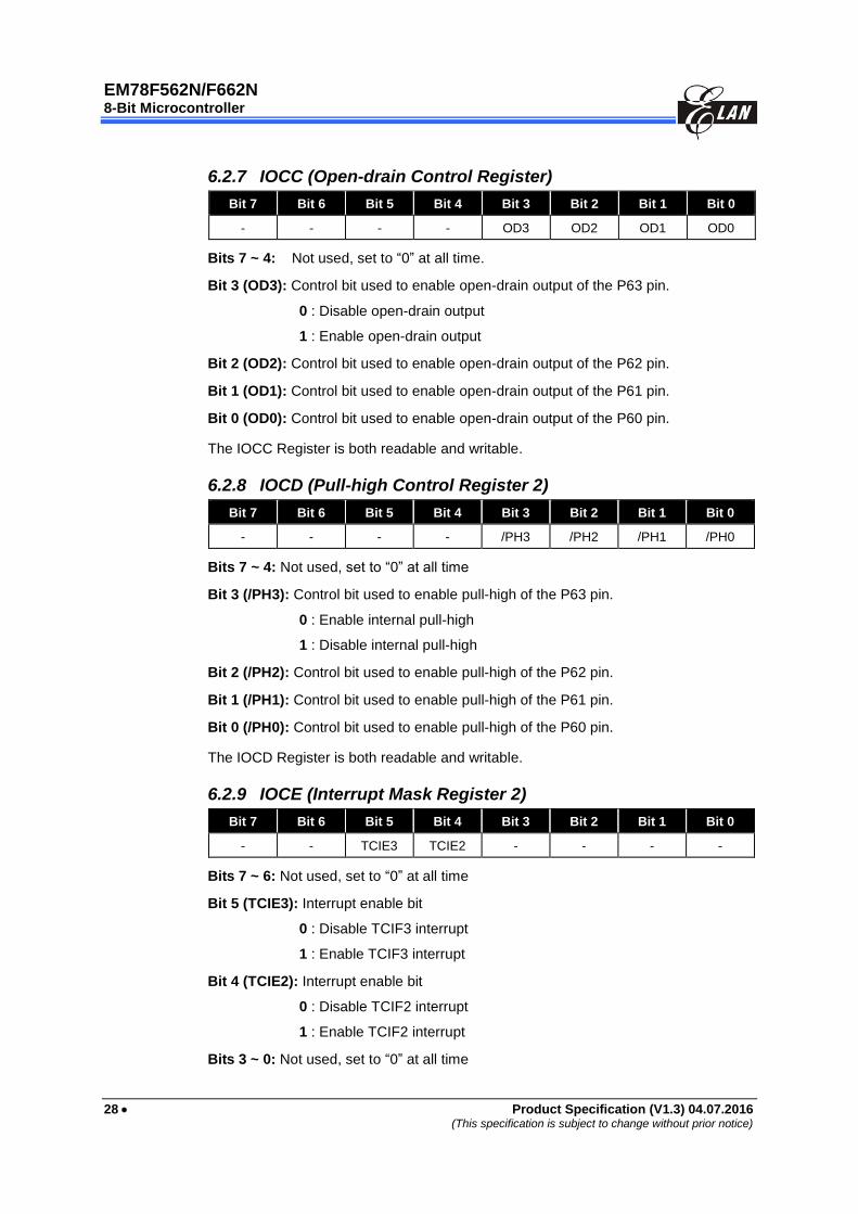
6.2.7 IOCC (Open-drain Control Register)
Bit 7 Bit 6 Bit 5 Bit 4 Bit 3 Bit 2 Bit 1 Bit 0
- - - - OD3 OD2 OD1 OD0
Bits 7 ~ 4: Not used, set to “0” at all time.
Bit 3 (OD3): Control bit used to enable open-drain output of the P63 pin.
0 : Disable open-drain output
1 : Enable open-drain output
Bit 2 (OD2): Control bit used to enable open-drain output of the P62 pin.
Bit 1 (OD1): Control bit used to enable open-drain output of the P61 pin.
Bit 0 (OD0): Control bit used to enable open-drain output of the P60 pin.
The IOCC Register is both readable and writable.
6.2.8 IOCD (Pull-high Control Register 2)
Bit 7 Bit 6 Bit 5 Bit 4 Bit 3 Bit 2 Bit 1 Bit 0
- - - - /PH3 /PH2 /PH1 /PH0
Bits 7 ~ 4: Not used, set to “0” at all time
Bit 3 (/PH3): Control bit used to enable pull-high of the P63 pin.
0 : Enable internal pull-high
1 : Disable internal pull-high
Bit 2 (/PH2): Control bit used to enable pull-high of the P62 pin.
Bit 1 (/PH1): Control bit used to enable pull-high of the P61 pin.
Bit 0 (/PH0): Control bit used to enable pull-high of the P60 pin.
The IOCD Register is both readable and writable.
6.2.9 IOCE (Interrupt Mask Register 2)
Bit 7 Bit 6 Bit 5 Bit 4 Bit 3 Bit 2 Bit 1 Bit 0
- - TCIE3 TCIE2 - - - -
Bits 7 ~ 6: Not used, set to “0” at all time
Bit 5 (TCIE3): Interrupt enable bit
0 : Disable TCIF3 interrupt
1 : Enable TCIF3 interrupt
Bit 4 (TCIE2): Interrupt enable bit
0 : Disable TCIF2 interrupt
1 : Enable TCIF2 interrupt
Bits 3 ~ 0: Not used, set to “0” at all time
EM78F562N/F662N
8-Bit Microcontroller
Product Specification (V1.3) 04.07.2016 29 (This specification is subject to change without prior notice)
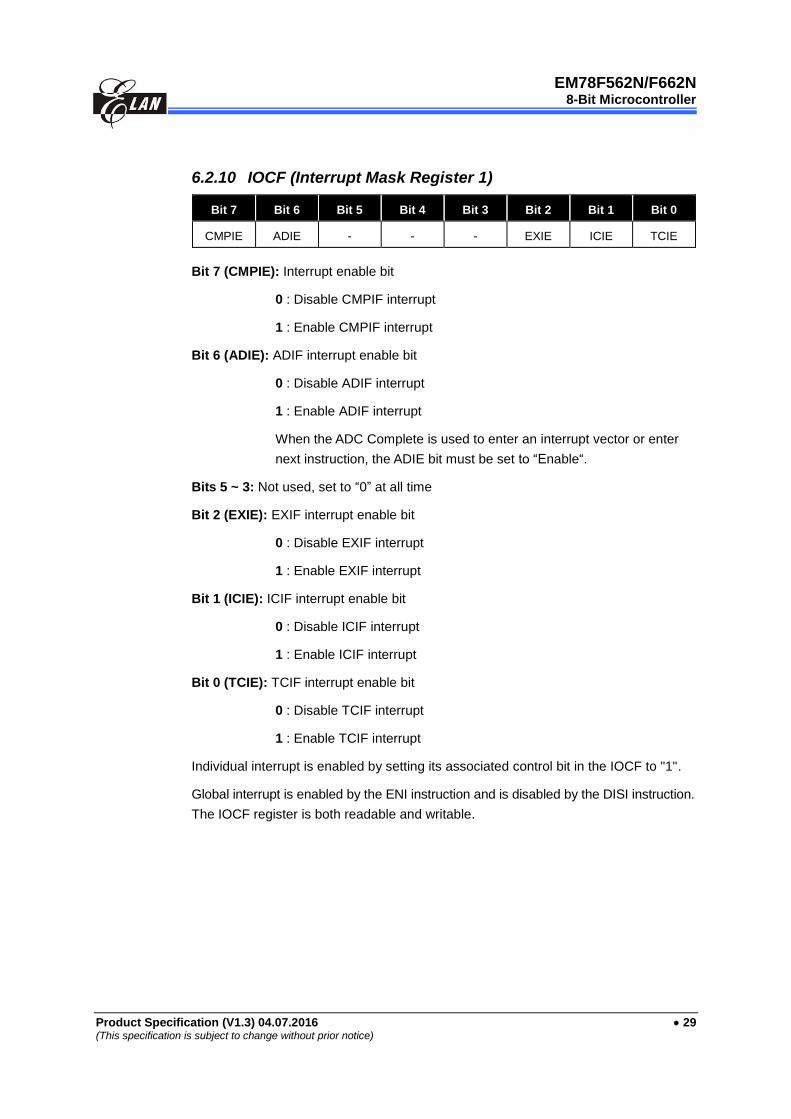
6.2.10 IOCF (Interrupt Mask Register 1)
Bit 7 Bit 6 Bit 5 Bit 4 Bit 3 Bit 2 Bit 1 Bit 0
CMPIE ADIE - - - EXIE ICIE TCIE
Bit 7 (CMPIE): Interrupt enable bit
0 : Disable CMPIF interrupt
1 : Enable CMPIF interrupt
Bit 6 (ADIE): ADIF interrupt enable bit
0 : Disable ADIF interrupt
1 : Enable ADIF interrupt
When the ADC Complete is used to enter an interrupt vector or enter
next instruction, the ADIE bit must be set to “Enable“.
Bits 5 ~ 3: Not used, set to “0” at all time
Bit 2 (EXIE): EXIF interrupt enable bit
0 : Disable EXIF interrupt
1 : Enable EXIF interrupt
Bit 1 (ICIE): ICIF interrupt enable bit
0 : Disable ICIF interrupt
1 : Enable ICIF interrupt
Bit 0 (TCIE): TCIF interrupt enable bit
0 : Disable TCIF interrupt
1 : Enable TCIF interrupt
Individual interrupt is enabled by setting its associated control bit in the IOCF to "1".
Global interrupt is enabled by the ENI instruction and is disabled by the DISI instruction.
The IOCF register is both readable and writable.

EM78F562N/F662N
8-Bit Microcontroller
30 Product Specification (V1.3) 04.07.2016
(This specification is subject to change without prior notice)
6.3 TCC/WDT and Prescaler
There are two 8-bit counters available as prescalers for the TCC and WDT respectively.
The PST0~PST2 bits of the CONT register are used to determine the ratio of the TCC
prescaler. Likewise, the PSW0~PSW2 bits of the IOCA register are used to determine
the WDT prescaler. The prescaler counter will be cleared by the instructions each time
they are written into TCC. The WDT and prescaler will be cleared by the “WDTC” and
“SLEP” instructions. Figure 6-11 depicts the circuit diagram of TCC/WDT.
R1 (TCC) is an 8-bit timer/counter. The TCC clock source can be the internal clock or
external signal input (edge selectable from the TCC pin). If the TCC signal source is from the
internal clock, the TCC will be incremented by 1 at the Fc clock (without prescaler). As
illustrated in Figure 6-11, selection of Fc depends on Bank 0 RE.6 <TIMERSC>. If the TCC
signal source is from an external clock input, the TCC will be incremented by 1 at every falling
edge or rising edge of the TCC pin. The TCC pin input time length (kept in high or low level)
must be greater than 1CLK. The TCC will stop running when sleep mode occurs.
The watchdog timer is a free running on-chip RC oscillator. WDT will keep on running
even after the oscillator driver has been turned off (i.e. in sleep mode). During normal
operation or sleep mode, a WDT time-out (if enabled) will cause the device to reset.
WDT can be enabled or disabled at any time during normal mode by software
programming. Refer to WDTE bit of the IOCA register. With no prescaler, the WDT
time-out period is approximately 18 ms1 (one oscillator start-up timer period).
(IOCC1)
PSW0~PSW2
PST2~PST 0
Fc
WDTE
(in IOCA)
Figure 6-11 Block Diagram of TCC and WDT
1 VDD=5V, WDT time-out period = 16.5ms ± 5%
VDD=3V, WDT time-out period = 18ms ± 5%.
EM78F562N/F662N
8-Bit Microcontroller
Product Specification (V1.3) 04.07.2016 31 (This specification is subject to change without prior notice)
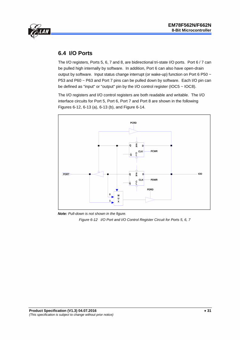
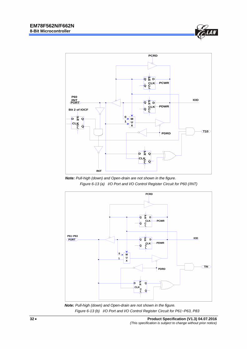
6.4 I/O Ports
The I/O registers, Ports 5, 6, 7 and 8, are bidirectional tri-state I/O ports. Port 6 / 7 can
be pulled high internally by software. In addition, Port 6 can also have open-drain
output by software. Input status change interrupt (or wake-up) function on Port 6 P50 ~
P53 and P60 ~ P63 and Port 7 pins can be pulled down by software. Each I/O pin can
be defined as "input" or "output" pin by the I/O control register (IOC5 ~ IOC8).
The I/O registers and I/O control registers are both readable and writable. The I/O
interface circuits for Port 5, Port 6, Port 7 and Port 8 are shown in the following
Figures 6-12, 6-13 (a), 6-13 (b), and Figure 6-14.
PCWR
PCRD
PDWR
PDRD
IOD
0
1
M
U
X
PORT Q
Q
_
D
DQ
Q_
CLK
PR
CL
CLK
PR
CL
Note: Pull-down is not shown in the figure.
Figure 6-12 I/O Port and I/O Control Register Circuit for Ports 5, 6, 7
EM78F562N/F662N
8-Bit Microcontroller
32 Product Specification (V1.3) 04.07.2016
(This specification is subject to change without prior notice)
PCRD
IOD
PCWR
PDWR
PDRD
Bit 2 of IOCF
PORT
P60
/INT
T10
INT
M
U
X
0
1
CLK
CLK
CLK
CLK
P
P
P
PR
R
R
R
CL
L
L
L
C
C
C
Q
Q
Q
Q
Q
Q
Q
Q
D
D
D
D
_
_
_
_
Note: Pull-high (down) and Open-drain are not shown in the figure.
Figure 6-13 (a) I/O Port and I/O Control Register Circuit for P60 (/INT)
PCRD
PCWR
PDWR
PDRDTIN
IODP61~P63
PORT
0
1
M
U
X
CLK
CLK
CLK
P
P
P
L
L
L
R
R
R
C
C
C
D
D
D
Q
Q
Q
Q
Q
Q
_
_
_
Note: Pull-high (down) and Open-drain are not shown in the figure.
Figure 6-13 (b) I/O Port and I/O Control Register Circuit for P61~P63, P83

EM78F562N/F662N
8-Bit Microcontroller
Product Specification (V1.3) 04.07.2016 33 (This specification is subject to change without prior notice)
/SLEP
T17
T10T11
IOCE.1
Interrupt
ENI Instruction
DISI Instruction
Interrupt
(Wake-up from SLEEP)
Next Instruction
(Wake-up from SLEEP)
CLK
CLK
CLK
Q
Q
Q
Q
Q
Q_
_
_
D
D
DP
P
P
L
L
L
R
R
R
C
C
C
RE.1
Figure 6-14 Block Diagram of I/O Port 6 with Input Change Interrupt/Wake-up
Table 6-1 Usage of Port 6 Input Change Wake-up/Interrupt Function
Usage of Port 6 Input Status Changed Wake-up/Interrupt
(I) Wake-up from Port 6 Input Status Change (II) Port 6 Input Status Change Interrupt
(a) Before Sleep 1. Read I/O Port 6 (MOV R6,R6)
1. Disable WDT2 (use this very carefully) 2. Execute "ENI"
2. Read I/O Port 6 (MOV R6,R6) 3. Enable interrupt (Set IOCF.1)
3 a. Enable interrupt (Set IOCF.1), after
wake-up if “ENI” switches to Interrupt
Vector (006H), if “DISI” excutes the
next instruction
4. IF Port 6 change (interrupt) Interrupt Vector (006H)
3 b. Disable interrupt (Set IOCF.1), always
execute next instruction
4. Enable wake-up enable bit (Set RA.6)
5. Execute "SLEP" instruction
(b) After Wake-up
1. IF "ENI" Interrupt vector (006H)
2. IF "DISI" Next instruction
2 The Software disables the WDT (Watchdog Timer) but the hardware must be enabled before
applying Port 6 Change Wake-up function. Set the Code Option Register Word 0 Bit 6
(ENWDTB) to “1”. 3 Vdd = 5V, set up time period = 16.8ms ± 8%
EM78F562N/F662N
8-Bit Microcontroller
34 Product Specification (V1.3) 04.07.2016
(This specification is subject to change without prior notice)
6.5 Reset and Wake-up
6.5.1 Reset
A reset is initiated by one of the following events:
(1) Power-on reset
(2) /RESET pin input "low"
(3) WDT time-out (if enabled)
The device is kept in a reset condition for a period of approximately 18ms3 (one
oscillator start-up timer period) after the reset is detected. Once a reset occurs, the
following functions are performed. Refer to Figure 6-8.
The oscillator is running, or will be started.
The Program Counter (R2) is set to all "0".
All I/O port pins are configured as input mode (high-impedance state).
The Watchdog Timer and prescaler are cleared.
When power is switched on, the upper three bits of R3 are cleared.
The bits of the RB, RC, RD, RD, RE registers are set to their previous status.
The bits of the CONT register are set to all "0" except for Bit 6 (INT flag).
The bits of the Pull-high, Pull-down.
Bank 0 RF, IOCF registers are cleared.
Sleep (power down) mode is asserted by executing the “SLEP” instruction. While
entering sleep mode, WDT (if enabled) is cleared but keeps on running. After a
wake-up, in RC mode the wake-up time is 34 clocks. High crystal mode wake-up time
is 2 ms and 32 clocks. In low Crystal 2 mode, wake-up time is 500 ms.
The controller can be awakened by:
(1) External reset input on /RESET pin
(2) WDT time-out (if enabled)
(3) Port 6 input status changes (if enabled)
(4) External (P60, /INT) pin changes (if EXWE is enabled)
(5) A/D conversion completed (if ADWE is enabled)
(6) Comparator output status change (if CMPWE is enabled)
Vdd = 3V, set up time period = 18ms ± 8%

EM78F562N/F662N
8-Bit Microcontroller
Product Specification (V1.3) 04.07.2016 35 (This specification is subject to change without prior notice)
The first two cases will cause the EM78F562N/F662N to reset. The T and P flags of R3
can be used to determine the source of the reset (wake-up). Cases 3 ~ 5 are considered
the continuation of program execution and the global interrupt ("ENI" or "DISI" being
executed) determines whether or not the controller branches to the interrupt vector
following wake-up. If ENI is executed before SLEP, the instruction will begin to execute
from Address 0x3, 0x6 0xF, 0x15 or 0X30, after wake-up. If DISI is executed before
SLEP, the execution will restart from the instruction right next to SLEP after wake-up. All
throughout the sleep mode, wake-up time is150 µs, no matter what oscillation mode
(except low Crystal mode). In low Crystal 2 mode, wake-up time is 500 ms.
Only one or more of Cases 2 to 5 can be enabled before entering into sleep mode.
That is,
[a] If WDT is enabled before SLEP, all of the RE bit is disabled. Hence, the
EM78F562N/F662N can be awakened only by Case 1 or 2. Refer to the Interrupt
section for further details.
[b] If Port 6 Input Status Change is used to wake up the EM78F562N/F662N and the
ICWE bit of the RA register is enabled before SLEP, WDT must be disabled.
Hence, the EM78F562N/F662N can be awakened only by Case 3.
[c] If External (P60,/INT) pin changes is used to wake-up the EM78F562N/F662N and
EXWE bit of the RA register is enabled before SLEP, WDT must be disabled by
software. Hence, the EM78F562N/F662N can be awakened only by Case 4.
[d] If AD conversion completed is used to wake-up EM78F562N/F662N and ADWE bit
of RA register is enabled before SLEP, the WDT must be disabled by software.
Hence, the EM78F562N/F662N can be awakened only by Case 5.
[e] If Comparator output status change is used to wake-up EM78F562N/F662N and
CMPWE bit of RA register is enabled before SLEP, WDT must be disabled by
software. Hence, the EM78F562N/F662N can be wakened only by Case 6.
If Port 6 Input Status Change Interrupt is used to wake up the EM78F562N/F662N, (as
in Case [a] above), the following instructions must be executed before SLEP:
MOV A, @001110xxb ; Select WDT prescaler and Disable
; WDT
IOW IOCA
WDTC ; Clear WDT and prescaler
MOV R6, R6 ; Read Port 6
ENI (or DISI) ; Enable (or disable) global
; interrupt
MOV A, @010xxxxxb ; Enable Port 6 input change
; wake-up bit
MOV RA,A
MOV A, @00000x1xb ; Enable Port 6 input change
; interrupt
IOW IOCF
SLEP ; Sleep
EM78F562N/F662N
8-Bit Microcontroller
36 Product Specification (V1.3) 04.07.2016
(This specification is subject to change without prior notice)
Similarly, if the Comparator Interrupt is used to wake up the EM78F562N/F662N (as in
Case [c] above), the following instructions must be executed before SLEP:
Bank 3 ; Select Bank 3
MOV A, @xxxxxx10b ; Select a comparator and P60 act
; as CO pin
MOV RB,A
MOV A, @001110xxb ; Select WDT prescaler and Disable
; WDT
IOW IOCA
WDTC ; Clear WDT and prescaler
ENI (or DISI) ; Enable (or disable) global
; interrupt
MOV A, @xxxxxx1xb ; Enable comparator output status
; change wake-up bit
MOV RA,A
MOV A, @10000000b ; Enable comparator output status
; change interrupt
IOW IOCF
SLEP ; Sleep

EM78F562N/F662N
8-Bit Microcontroller
Product Specification (V1.3) 04.07.2016 37 (This specification is subject to change without prior notice)
6.5.2 Wake-up
Summary of Wake-up and Interrupt Modes
All categories under Wake-up and Interrupt modes are summarized below.
The controller can be awakened from sleep mode and idle mode. The wake-up signals
are listed as follows.
Wake-up
Signal Sleep Mode Idle Mode Green Mode Normal Mode
External
interrupt
If EXWE bit is enabled
Wake-up + interrupt (if
interrupt is enabled)
+ next instruction
If EXWE bit is enabled
Wake-up + interrupt (if
interrupt is enabled) +
next instruction
Interrupt (if interrupt is
enabled)
or next instruction
Interrupt (if interrupt
is enabled)
or next instruction
Port 6 pin
change
If enable ICWE bit
Wake-up
+ interrupt (if interrupt is
enabled)
+ next instruction
If enable ICWE bit
Wake-up
+ interrupt (if interrupt is
enabled)
+ next instruction
Interrupt (if interrupt is
enabled)
or next instruction
Interrupt (if interrupt
is enabled)
or next instruction
TCC overflow
interrupt x
Wake-up + interrupt (if
interrupt is enabled)
+ next instruction
Interrupt (if interrupt is
enabled)
or next instruction
Interrupt (if interrupt
is enabled)
or next instruction
Comparator
interrupt
If CMPWE bit is
enabled
Wake-up + interrupt (if
interrupt is enabled)
+ next instruction
If CMPWE bit is enabled
Wake-up + interrupt (if
interrupt is enabled)
+ next instruction
Interrupt (if interrupt is
enabled)
or next instruction
Interrupt (if interrupt
is enabled)
or next instruction
AD
conversion
complete
interrupt
If ADWE bit is enabled
Wake-up + interrupt (if
interrupt is enabled)
+ next instruction
Fs and Fm don’t stop
If ADWE bit is enabled
Wake-up + interrupt (if
interrupt is enabled)
+ next instruction
Fs and Fm don’t stop
Interrupt (if interrupt is
enabled)
or next instruction
Fs and Fm don’t stop
Interrupt (if interrupt
is enabled)
or next instruction
TC2 interrupt x
Wake-up + interrupt (if
interrupt is enabled)
+ next instruction
Interrupt (if interrupt is
enabled)
or next instruction
Interrupt (if interrupt
is enabled)
or next instruction
TC3 interrupt x
Wake-up + interrupt (if
interrupt is enabled)
+ next instruction
Interrupt (if interrupt is
enabled)
or next instruction
Interrupt (if interrupt
is enabled)
or next instruction
WDT Time out RESET RESET RESET RESET
Low Voltage
Reset RESET RESET RESET RESET
After wake up:
1. If interrupt is enabled interrupt + next instruction
2. If interrupt is disabled next instruction

EM78F562N/F662N
8-Bit Microcontroller
38 Product Specification (V1.3) 04.07.2016
(This specification is subject to change without prior notice)
6.5.3 Summary of Register Initial Values after Reset
Legend: U: Unknown or don’t care P: Previous value before reset
x: Not used t: Check Table 6-2
Addr. Name Reset Type Bit 7 Bit 6 Bit 5 Bit 4 Bit 3 Bit 2 Bit 1 Bit 0
0x05 IOC5
Bit Name C57 C56 C55 C54 C53 C52 C51 C50
Power-on 1 1 1 1 1 1 1 1
/RESET and WDT 1 1 1 1 1 1 1 1
Wake-up from Pin Change P P P P P P P P
0x06 IOC6
Bit Name C63 C62 C61 C60
Power-on 0 0 0 0 1 1 1 1
/RESET and WDT 0 0 0 0 1 1 1 1
Wake-up from Pin Change 0 0 0 0 P P P P
0x07 IOC7
Bit Name C77 C73 C72 C71 C70
Power-on 1 0 0 0 1 1 1 1
/RESET and WDT 1 0 0 0 1 1 1 1
Wake-up from Pin Change P 0 0 0 P P P P
0x08 IOC8
Bit Name C83
Power-on 0 0 0 0 1 0 0 0
/RESET and WDT 0 0 0 0 1 0 0 0
Wake-up from Pin Change 0 0 0 0 P 0 0 0
N/A CONT
Bit Name INTE /INT TS TE PSTE PST2 PST1 PST0
Power-on 0 0 0 0 0 0 0 0
/RESET and WDT 0 0 0 0 0 0 0 0
Wake-up from Pin Change P P P P P P P P
000 R0
IAR
Bit Name IAR7 IAR6 IAR5 IAR4 IAR3 IAR2 IAR1 IAR0
Power-on U U U U U U U U
/RESET and WDT P P P P P P P P
Wake-up from Pin Change P P P P P P P P
001 R1
TCC
Bit Name TCC7 TCC6 TCC5 TCC4 TCC3 TCC2 TCC1 TCC0
Power-on 0 0 0 0 0 0 0 0
/RESET and WDT 0 0 0 0 0 0 0 0
Wake-up from Pin Change P P P P P P P P
002 R2
PC
Bit Name A7 A6 A5 A4 A3 A2 A1 A0
Power-on 0 0 0 0 0 0 0 0
/RESET and WDT 0 0 0 0 0 0 0 0
Wake-up from Pin Change P P P P P P P P
003 R3
SR
Bit Name T P Z DC C
Power-on 0 0 0 1 1 U U U
/RESET and WDT 0 0 0 t t P P P
Wake-up from Pin Change 0 0 0 t t P P P
004 R4
RSR
Bit Name RSR7 RSR6 RSR5 RSR4 RSR3 RSR2 RSR1 RSR0
Power-on U U U U U U U U
/RESET and WDT P P P P P P P P
Wake-up from Pin Change P P P P P P P P

EM78F562N/F662N
8-Bit Microcontroller
Product Specification (V1.3) 04.07.2016 39 (This specification is subject to change without prior notice)
(Continuation)
Addr. Name Reset Type Bit 7 Bit 6 Bit 5 Bit 4 Bit 3 Bit 2 Bit 1 Bit 0
005 Bank 0
P5
Bit Name P57 P56 P55 P54 P53 P52 P51 P50
Power-on 1 1 1 1 1 1 1 1
/RESET and WDT 1 1 1 1 1 1 1 1
Wake-up from Pin Change P P P P P P P P
006 Bank 0
P6
Bit Name x x x x P63 P62 P61 P60
Power-on 0 0 0 0 1 1 1 1
/RESET and WDT 0 0 0 0 1 1 1 1
Wake-up from Pin Change 0 0 0 0 P P P P
007 Bank 0
P7
Bit Name P77 x x x P73 P72 P71 P70
Power-on 1 0 0 0 1 1 1 1
/RESET and WDT 1 0 0 0 1 1 1 1
Wake-up from Pin Change P 0 0 0 P P P P
008 Bank 0
P8
Bit Name x x x x P83 x x x
Power-on 0 0 0 0 1 0 0 0
/RESET and WDT 0 0 0 0 1 0 0 0
Wake-up from Pin Change 0 0 0 0 P 0 0 0
009
Bank 0
R9
TBPTL
Bit Name RBit7 RBit6 RBit5 RBit4 RBit3 RBit2 RBit1 RBit0
Power-on 0 0 0 0 0 0 0 0
/RESET and WDT 0 0 0 0 0 0 0 0
Wake-up from Pin Change P P P P P P P P
00A
Bank 0
RA
WUCR
Bit Name x ICWE ADWE EXWE x x CMPWE x
Power-on 0 0 0 0 0 0 0 0
/RESET and WDT 0 0 0 0 0 0 0 0
Wake-up from Pin Change 0 P P P 0 0 0 0
00B
Bank 0
RB
ECR
Bit Name RD WR EEWE EEDF EEPC x x x
Power-on 0 0 0 0 0 0 0 0
/RESET and WDT P P P P P 0 0 0
Wake-up from Pin Change P P P P P 0 0 0
00C
Bank 0
RC
EA
Bit Name x EE_A6 EE_A5 EE_A4 EE_A3 EE_A2 EE_A1 EE_A0
Power-on 0 0 0 0 0 0 0 0
/RESET and WDT 0 P P P P P P P
Wake-up from Pin Change 0 P P P P P P P
00D
Bank 0
RD
ED
Bit Name EE_D7 EE_D6 EE_D5 EE_D4 EE_D3 EE_D2 EE_D1 EE_D0
Power-on 0 0 0 0 0 0 0 0
/RESET and WDT P P P P P P P P
Wake-up from Pin Change P P P P P P P P
00E
Bank 0
RE
CPUOCR
Bit Name x TIMERSC CPUS IDLE x x x x
Power-on 0 1 1 1 0 0 0 0
/RESET and WDT 0 1 1 1 0 0 0 0
Wake-up from Pin Change 0 P P P 0 0 0 0

EM78F562N/F662N
8-Bit Microcontroller
40 Product Specification (V1.3) 04.07.2016
(This specification is subject to change without prior notice)
(Continuation)
Addr Name Reset Type Bit 7 Bit 6 Bit 5 Bit 4 Bit 3 Bit 2 Bit 1 Bit 0
00F
Bank 0
RF
ISR
Bit Name CMPIF ADIF x x x EXIF ICIF TCIF
Power-on 0 0 0 0 0 0 0 0
/RESET and WDT 0 0 0 0 0 0 0 0
Wake-up from Pin Change P P 0 0 0 P P P
08
Bank 1
R8
TC2CR
Bit Name RCM1 RCM0 TC2ES TC2M TC2S TC2CK2 TC2CK1 TC2CK0
Power-on Option
RCM1
Option
RCM0 0 0 0 0 0 0
/RESET and WDT Option
RCM1
Option
RCM0 0 0 0 0 0 0
Wake-up from Pin Change P P P P P P P P
09
Bank 1
R9
TC2DH
Bit Name TC2D15 TC2D14 TC2D13 TC2D12 TC2D11 TC2D10 TC2D9 TC2D8
Power-on 0 0 0 0 0 0 0 0
/RESET and WDT 0 0 0 0 0 0 0 0
Wake-up from Pin Change P P P P P P P P
0A
Bank 1
RA
TC2DL
Bit Name TC2D7 TC2D6 TC2D5 TC2D4 TC2D3 TC2D2 TC2D1 TC2D0
Power-on 0 0 0 0 0 0 0 0
/RESET and WDT 0 0 0 0 0 0 0 0
Wake-up from Pin Change P P P P P P P P
0F
Bank 1
RF
ISR
Bit Name x x TCIF3 TCIF2 x x x x
Power-on 0 0 0 0 0 0 0 0
/RESET and WDT 0 0 0 0 0 0 0 0
Wake-up from Pin Change 0 0 0 0 0 0 0 0
005 R5
(Bank 2)
Bit Name ADE7 ADE6 ADE5 ADE4 ADE3 ADE2 ADE1 ADE0
Power-on 0 0 0 0 0 0 0 0
/RESET and WDT 0 0 0 0 0 0 0 0
Wake-up from Pin Change P P P P P P P P
006
Bank 2
R6
ADCON
Bit Name VREFS CKR1 CKR0 ADRUN ADPD ADIS2 ADIS1 ADIS0
Power-on 0 0 0 0 0 0 0 0
/RESET and WDT 0 0 0 0 0 0 0 0
Wake-up from Pin Change P P P P P P P P
07
Bank 2
R7
ADOC
Bit Name CALI SIGN VOF[2] VOF[1] VOF[0] x x x
Power-on 0 0 0 0 0 0 0 0
/RESET and WDT 0 0 0 0 0 0 0 0
Wake-up from Pin Change P P P P P 0 0 0
08
Bank 2
R8
ADDH
Bit Name ADD9 ADD8 ADD7 ADD6 ADD5 ADD4 ADD3 ADD2
Power-on 0 0 0 0 0 0 0 0
/RESET and WDT 0 0 0 0 0 0 0 0
Wake-up from Pin Change P P P P P P P P

EM78F562N/F662N
8-Bit Microcontroller
Product Specification (V1.3) 04.07.2016 41 (This specification is subject to change without prior notice)
(Continuation)
Addr. Name Reset Type Bit 7 Bit 6 Bit 5 Bit 4 Bit 3 Bit 2 Bit 1 Bit 0
09
Bank 2
R9
ADDL
Bit Name x x x x x x ADD1 ADD0
Power-on 0 0 0 0 0 0 0 0
/RESET and WDT 0 0 0 0 0 0 0 0
Wake-up from Pin Change 0 0 0 0 0 0 P P
00B
Bank 2
RB
CMPCON
Bit Name x x x x x CPOUT CPS1 CPS0
Power-on 0 0 0 0 0 0 0 0
/RESET and WDT 0 0 0 0 0 0 0 0
Wake-up from Pin Change 0 0 0 0 0 P P P
00F
Bank 2
RF
PHCR1
Bit Name x x x x /PH73 /PH72 /PH71 /PH70
Power-on 0 0 0 0 1 1 1 1
/RESET and WDT 0 0 0 0 1 1 1 1
Wake-up from Pin Change 0 0 0 0 P P P P
006
Bank 3
R6
TBPTH
Bit Name MLB x x x x RBit 10 RBit 9 RBit 8
Power-on 0 0 0 0 0 0 0 0
/RESET and WDT 0 0 0 0 0 0 0 0
Wake-up from Pin Change P 0 0 0 0 P P P
0D
Bank 3
RD
TC3CR
Bit Name TC3FF1 TC3FF0 TC3S TC3CK2 TC3CK1 TC3CK0 TC3M1 TC3M0
Power-on 0 0 0 0 0 0 0 0
/RESET and WDT 0 0 0 0 0 0 0 0
Wake-up from Pin Change P P P P P P P P
0E
Bank 3
RE
TC3D
Bit Name TC3D7 TC3D6 TC3D5 TC3D4 TC3D3 TC3D2 TC3D1 TC3D0
Power-on 0 0 0 0 0 0 0 0
/RESET and WDT 0 0 0 0 0 0 0 0
Wake-up from Pin Change P P P P P P P P
0F
Bank 3
RF
PDCR1
Bit Name x x x x /PD73 /PD72 /PD71 /PD70
Power-on 0 0 0 0 1 1 1 1
/RESET and WDT 0 0 0 0 1 1 1 1
Wake-up from Pin Change 0 0 0 0 P P P P
00A IOCA
WDTCR
Bit Name WDTE EIS x x PSWE PSW2 PSW1 PSW0
Power-on 0 0 0 0 0 0 0 0
/RESET and WDT 0 0 0 0 0 0 0 0
Wake-up from Pin Change P P 0 0 P P P P
00B IOCB
PDCR2
Bit Name /PD7 /PD6 /PD5 /PD4 /PD3 /PD2 /PD1 /PD0
Power-on 1 1 1 1 1 1 1 1
/RESET and WDT 1 1 1 1 1 1 1 1
Wake-up from Pin Change P P P P P P P P
00C IOCC
ODCR
Bit Name x x x x OD3 OD2 OD1 OD0
Power-on 0 0 0 0 0 0 0 0
/RESET and WDT 0 0 0 0 0 0 0 0
Wake-up from Pin Change 0 0 0 0 P P P P
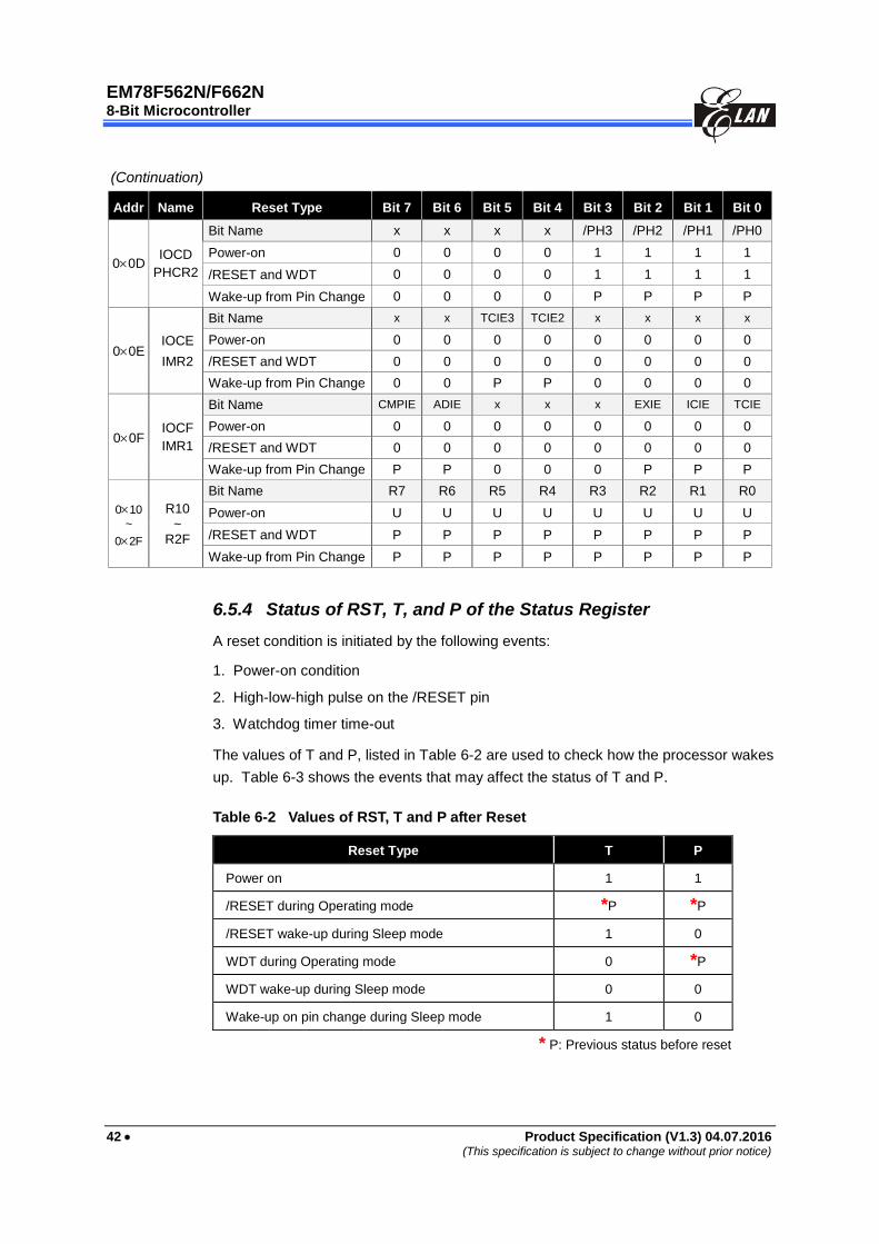
EM78F562N/F662N
8-Bit Microcontroller
42 Product Specification (V1.3) 04.07.2016
(This specification is subject to change without prior notice)
(Continuation)
Addr Name Reset Type Bit 7 Bit 6 Bit 5 Bit 4 Bit 3 Bit 2 Bit 1 Bit 0
00D IOCD
PHCR2
Bit Name x x x x /PH3 /PH2 /PH1 /PH0
Power-on 0 0 0 0 1 1 1 1
/RESET and WDT 0 0 0 0 1 1 1 1
Wake-up from Pin Change 0 0 0 0 P P P P
00E IOCE
IMR2
Bit Name x x TCIE3 TCIE2 x x x x
Power-on 0 0 0 0 0 0 0 0
/RESET and WDT 0 0 0 0 0 0 0 0
Wake-up from Pin Change 0 0 P P 0 0 0 0
00F IOCF
IMR1
Bit Name CMPIE ADIE x x x EXIE ICIE TCIE
Power-on 0 0 0 0 0 0 0 0
/RESET and WDT 0 0 0 0 0 0 0 0
Wake-up from Pin Change P P 0 0 0 P P P
010
~
02F
R10 ~
R2F
Bit Name R7 R6 R5 R4 R3 R2 R1 R0
Power-on U U U U U U U U
/RESET and WDT P P P P P P P P
Wake-up from Pin Change P P P P P P P P
6.5.4 Status of RST, T, and P of the Status Register
A reset condition is initiated by the following events:
1. Power-on condition
2. High-low-high pulse on the /RESET pin
3. Watchdog timer time-out
The values of T and P, listed in Table 6-2 are used to check how the processor wakes
up. Table 6-3 shows the events that may affect the status of T and P.
Table 6-2 Values of RST, T and P after Reset
Reset Type T P
Power on 1 1
/RESET during Operating mode *P *P
/RESET wake-up during Sleep mode 1 0
WDT during Operating mode 0 *P
WDT wake-up during Sleep mode 0 0
Wake-up on pin change during Sleep mode 1 0
* P: Previous status before reset
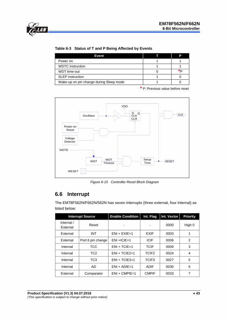
EM78F562N/F662N
8-Bit Microcontroller
Product Specification (V1.3) 04.07.2016 43 (This specification is subject to change without prior notice)
Table 6-3 Status of T and P Being Affected by Events
Event T P
Power on 1 1
WDTC instruction 1 1
WDT time-out 0 *P
SLEP instruction 1 0
Wake-up on pin change during Sleep mode 1 0
* P: Previous value before reset
Voltage
Detector
Power-on
Reset
WDTE
Setup
Time
VDD
D QCLKCLR
CLK
RESETWDT
TimeoutWDT
/RESET
Oscillator
Figure 6-15 Controller Reset Block Diagram
6.6 Interrupt
The EM78F562N/F662N/562N has seven interrupts (three external, four internal) as
listed below:
Interrupt Source Enable Condition Int. Flag Int. Vector Priority
Internal /
External Reset - - 0000 High 0
External INT ENI + EXIE=1 EXIF 0003 1
External Port 6 pin change ENI +ICIE=1 ICIF 0006 2
Internal TCC ENI + TCIE=1 TCIF 0009 3
Internal TC2 ENI + TCIE2=1 TCIF2 0024 4
Internal TC3 ENI + TCIE3=1 TCIF3 0027 5
Internal AD ENI + ADIE=1 ADIF 0030 6
External Comparator ENI + CMPIE=1 CMPIF 0033 7
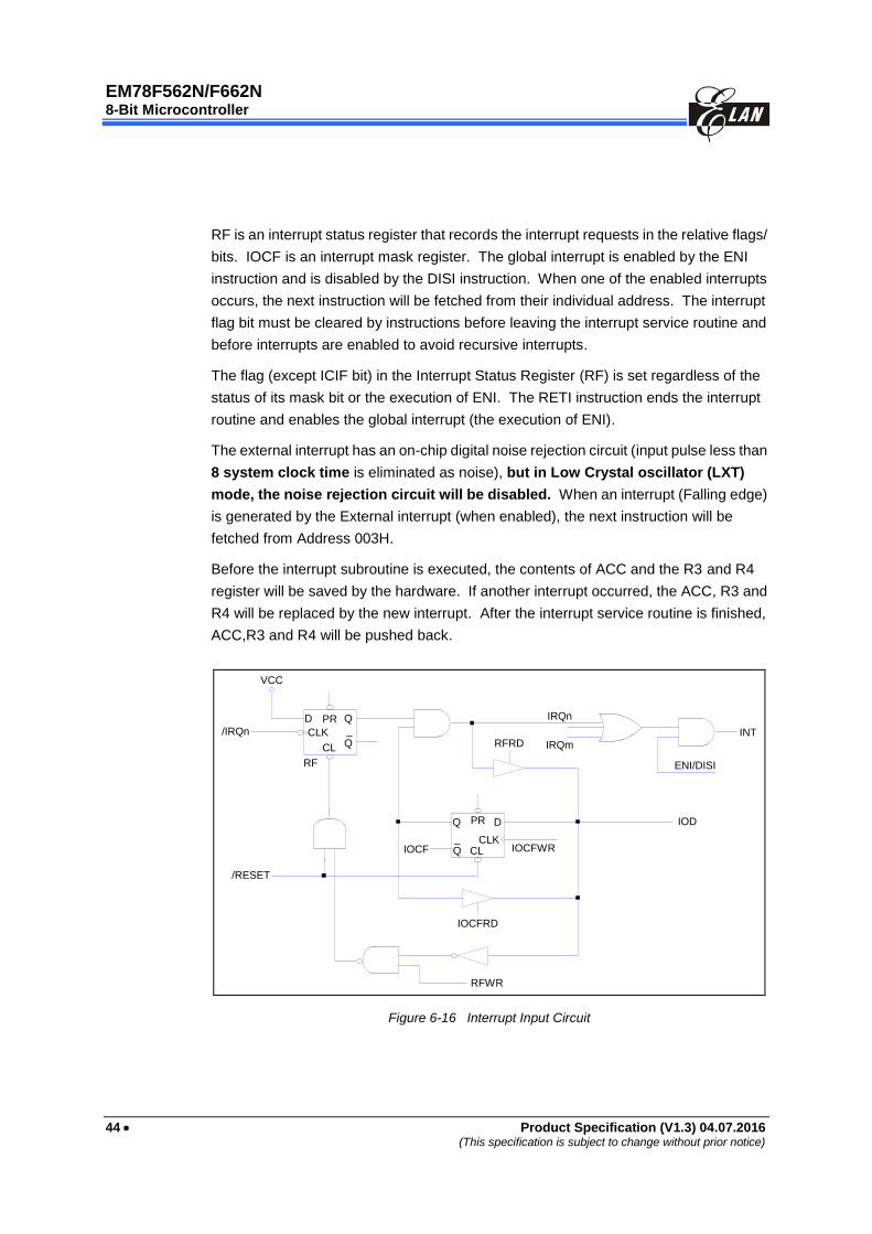
EM78F562N/F662N
8-Bit Microcontroller
44 Product Specification (V1.3) 04.07.2016
(This specification is subject to change without prior notice)
RF is an interrupt status register that records the interrupt requests in the relative flags/
bits. IOCF is an interrupt mask register. The global interrupt is enabled by the ENI
instruction and is disabled by the DISI instruction. When one of the enabled interrupts
occurs, the next instruction will be fetched from their individual address. The interrupt
flag bit must be cleared by instructions before leaving the interrupt service routine and
before interrupts are enabled to avoid recursive interrupts.
The flag (except ICIF bit) in the Interrupt Status Register (RF) is set regardless of the
status of its mask bit or the execution of ENI. The RETI instruction ends the interrupt
routine and enables the global interrupt (the execution of ENI).
The external interrupt has an on-chip digital noise rejection circuit (input pulse less than
8 system clock time is eliminated as noise), but in Low Crystal oscillator (LXT)
mode, the noise rejection circuit will be disabled. When an interrupt (Falling edge)
is generated by the External interrupt (when enabled), the next instruction will be
fetched from Address 003H.
Before the interrupt subroutine is executed, the contents of ACC and the R3 and R4
register will be saved by the hardware. If another interrupt occurred, the ACC, R3 and
R4 will be replaced by the new interrupt. After the interrupt service routine is finished,
ACC,R3 and R4 will be pushed back.
INT
ENI/DISI
IOD
RFWR
IOCFRD
IOCFWR
IRQn
IRQmRFRD
IOCF
/RESET
/IRQn
VCC
RF
CLK
CLK
Q
Q
DPR
CL_
PR
CL
Q
Q_
D
Figure 6-16 Interrupt Input Circuit
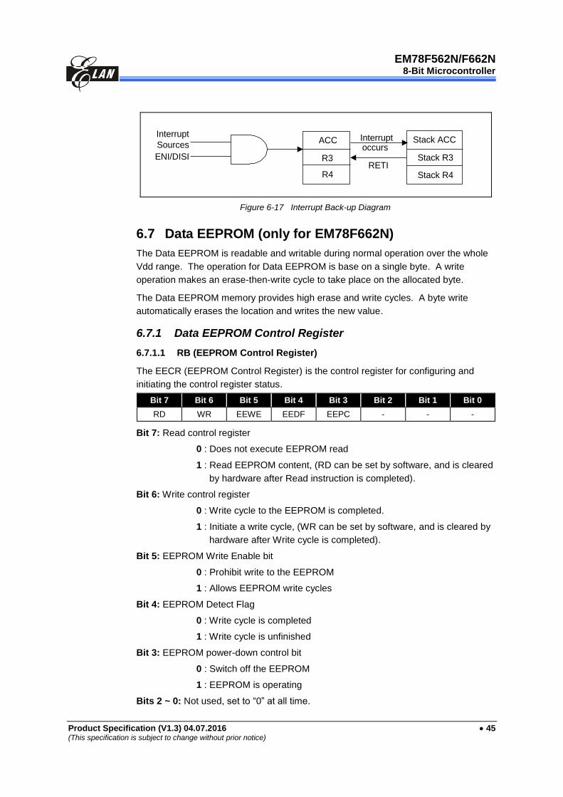
EM78F562N/F662N
8-Bit Microcontroller
Product Specification (V1.3) 04.07.2016 45 (This specification is subject to change without prior notice)
Interrupt
SourcesInterrupt
occurs
ENI/DISI
Stack ACC
Stack R3
RETI
ACC
R3
R4 Stack R4
Figure 6-17 Interrupt Back-up Diagram
6.7 Data EEPROM (only for EM78F662N)
The Data EEPROM is readable and writable during normal operation over the whole
Vdd range. The operation for Data EEPROM is base on a single byte. A write
operation makes an erase-then-write cycle to take place on the allocated byte.
The Data EEPROM memory provides high erase and write cycles. A byte write
automatically erases the location and writes the new value.
6.7.1 Data EEPROM Control Register
6.7.1.1 RB (EEPROM Control Register)
The EECR (EEPROM Control Register) is the control register for configuring and
initiating the control register status.
Bit 7 Bit 6 Bit 5 Bit 4 Bit 3 Bit 2 Bit 1 Bit 0
RD WR EEWE EEDF EEPC - - -
Bit 7: Read control register
0 : Does not execute EEPROM read
1 : Read EEPROM content, (RD can be set by software, and is cleared
by hardware after Read instruction is completed).
Bit 6: Write control register
0 : Write cycle to the EEPROM is completed.
1 : Initiate a write cycle, (WR can be set by software, and is cleared by
hardware after Write cycle is completed).
Bit 5: EEPROM Write Enable bit
0 : Prohibit write to the EEPROM
1 : Allows EEPROM write cycles
Bit 4: EEPROM Detect Flag
0 : Write cycle is completed
1 : Write cycle is unfinished
Bit 3: EEPROM power-down control bit
0 : Switch off the EEPROM
1 : EEPROM is operating
Bits 2 ~ 0: Not used, set to “0” at all time.

EM78F562N/F662N
8-Bit Microcontroller
46 Product Specification (V1.3) 04.07.2016
(This specification is subject to change without prior notice)
6.7.1.2 RC (128 Bytes EEPROM Address)
When accessing the EEPROM data memory, RC (128 bytes EEPROM address
register) holds the address to be accessed. In accordance with the operation, RD
(128 bytes EEPROM Data register) holds the data to be written, or the data read, at the
address in RC.
Bit 7 Bit 6 Bit 5 Bit 4 Bit 3 Bit 2 Bit 1 Bit 0
- EE_A6 EE_A5 EE_A4 EE_A3 EE_A2 EE_A1 EE_A0
Bit 7: Not used, set to “0” at all time.
Bits 6 ~ 0: 128 bytes EEPROM address
6.7.1.3 RD (256 Bytes EEPROM Data)
Bit 7 Bit 6 Bit 5 Bit 4 Bit 3 Bit 2 Bit 1 Bit 0
EE_D7 EE_D6 EE_D5 EE_D4 EE_D3 EE_D2 EE_D1 EE_D0
Bits 7 ~ 0: 128 bytes EEPROM data
6.7.2 Programming Step / Example Demonstration
6.7.2.1 Programming Step
Follow these steps to write or read data from the EEPROM:
(1) Set the RB.EEPC bit to “1” to enable the EEPROM power.
(2) Write the address to RC (128 bytes EEPROM address).
a.1. Set the RB.EEWE bit to “1”, if the write function is employed.
a.2. Write the 8-bit data value to be programmed in the RD (256 bytes EEPROM
data)
a.3. Set the RB.WR bit to ”1”, then execute write function
b. Set the RB.READ bit to ”1”, after which, execute read function
(3) a. Wait for the RB.EEDF or RB.WR to be cleared
b. Wait for the RB.EEDF to be cleared
(4) For the next conversion, go to Step 2 as required.
(5) If user wants to conserve power and to make sure the EEPROM data is not used,
clear the RB.EEPC.
6.7.2.2 Example Demonstration Programs
; To define the control register
; Write data to EEPROM
RC == 0x0C
RB == 0x0B
RD == 0x0D
Read == 0x07
WR == 0x06
EEWE == 0x05
EEDF == 0x04
EEPC == 0x03
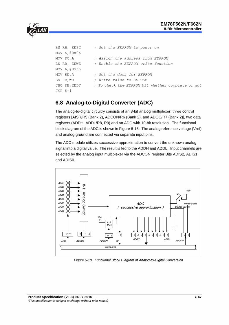
EM78F562N/F662N
8-Bit Microcontroller
Product Specification (V1.3) 04.07.2016 47 (This specification is subject to change without prior notice)
BS RB, EEPC ; Set the EEPROM to power on
MOV A,@0x0A
MOV RC,A ; Assign the address from EEPROM
BS RB, EEWE ; Enable the EEPROM write function
MOV A,@0x55
MOV RD,A ; Set the data for EEPROM
BS RB,WR ; Write value to EEPROM
JBC RB,EEDF ; To check the EEPROM bit whether complete or not
JMP $-1
6.8 Analog-to-Digital Converter (ADC)
The analog-to-digital circuitry consists of an 8-bit analog multiplexer, three control
registers [AISR/R5 (Bank 2), ADCON/R6 (Bank 2), and ADOC/R7 (Bank 2)], two data
registers (ADDH, ADDL/R8, R9) and an ADC with 10-bit resolution. The functional
block diagram of the ADC is shown in Figure 6-18. The analog reference voltage (Vref)
and analog ground are connected via separate input pins.
The ADC module utilizes successive approximation to convert the unknown analog
signal into a digital value. The result is fed to the ADDH and ADDL. Input channels are
selected by the analog input multiplexer via the ADCON register Bits ADIS2, ADIS1
and ADIS0.
ADDH
DATA BUS
ADC2
ADC1
ADC0
ADC3
Vref
Power- Down
Fsco
4 - 1
MUX
7 ~ 0 34
ADC( successive approximation )
656
ADCON RFAISR ADCON
Start to Convert
01
ADCON
8-1
An
alo
g S
witc
h
0123456789
ADDL
ADC6
ADC5
ADC4
ADC7
2
Figure 6-18 Functional Block Diagram of Analog-to-Digital Conversion

EM78F562N/F662N
8-Bit Microcontroller
48 Product Specification (V1.3) 04.07.2016
(This specification is subject to change without prior notice)
6.8.1 ADC Control Register (AISR/R5, ADCON/R6, ADOC/R7)
6.8.1.1 Bank 2 R5 AISR (ADC Input Select Register)
The AISR register individually defines the ADC pins as analog input or as digital I/O.
Bit 7 Bit 6 Bit 5 Bit 4 Bit 3 Bit 2 Bit 1 Bit 0
ADE7 ADE6 ADE5 ADE4 ADE3 ADE2 ADE1 ADE0
Bit 7 (ADE7): AD converter enable bit of the P57 pin.
0 : Disable ADC7, P57 act as I/O pin.
1 : Enable ADC7 to act as analog input pin
Bit 6 (ADE6): AD converter enable bit of the P56 pin.
0 : Disable ADC6, P56 act as I/O pin
1 : Enable ADC6 to act as analog input pin
Bit 5 (ADE5): AD converter enable bit of the P77 pin
0 : Disable ADC5, P77 functions as I/O pin
1 : Enable ADC5 to function as analog input pin
Bit 4 (ADE4): AD converter enable bit of the P73 pin
0 : Disable ADC4, P73 act as I/O pin
1 : Enable ADC4 to act as analog input pin
Bit 3 (ADE3): AD converter enable bit of the P63 pin.
0 : Disable ADC3, P63 act as I/O pin
1 : Enable ADC3 to act as analog input pin
Bit 2 (ADE2): AD converter enable bit of the P62 pin.
0 : Disable ADC2, P62 act as I/O pin
1 : Enable ADC2 to act as analog input pin
Bit 1 (ADE1): AD converter enable bit of the P61 pin
0 : Disable ADC1, P61 functions as I/O pin
1 : Enable ADC1 to function as analog input pin
Bit 0 (ADE0): AD converter enable bit of the P60 pin
0 : Disable ADC0, P60 act as I/O pin
1 : Enable ADC0 to act as analog input pin
The following table shows the priority of P60/ADC0//INT.
P60/ADC0//Int Pin Priority
Hight Medium Low
/INT AD0 P60
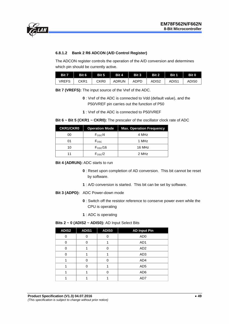
EM78F562N/F662N
8-Bit Microcontroller
Product Specification (V1.3) 04.07.2016 49 (This specification is subject to change without prior notice)
6.8.1.2 Bank 2 R6 ADCON (A/D Control Register)
The ADCON register controls the operation of the A/D conversion and determines
which pin should be currently active.
Bit 7 Bit 6 Bit 5 Bit 4 Bit 3 Bit 2 Bit 1 Bit 0
VREFS CKR1 CKR0 ADRUN ADPD ADIS2 ADIS1 ADIS0
Bit 7 (VREFS): The input source of the Vref of the ADC.
0 : Vref of the ADC is connected to Vdd (default value), and the
P50/VREF pin carries out the function of P50
1 : Vref of the ADC is connected to P50/VREF
Bit 6 ~ Bit 5 (CKR1 ~ CKR0): The prescaler of the oscillator clock rate of ADC
CKR1/CKR0 Operation Mode Max. Operation Frequency
00 FOSC/4 4 MHz
01 FOSC 1 MHz
10 FOSC/16 16 MHz
11 FOSC/2 2 MHz
Bit 4 (ADRUN): ADC starts to run
0 : Reset upon completion of AD conversion. This bit cannot be reset
by software.
1 : A/D conversion is started. This bit can be set by software.
Bit 3 (ADPD): ADC Power-down mode
0 : Switch off the resistor reference to conserve power even while the
CPU is operating
1 : ADC is operating
Bits 2 ~ 0 (ADIS2 ~ ADIS0): AD Input Select Bits
ADIS2 ADIS1 ADIS0 AD Input Pin
0 0 0 AD0
0 0 1 AD1
0 1 0 AD2
0 1 1 AD3
1 0 0 AD4
1 0 1 AD5
1 1 0 AD6
1 1 1 AD7

EM78F562N/F662N
8-Bit Microcontroller
50 Product Specification (V1.3) 04.07.2016
(This specification is subject to change without prior notice)
6.8.1.3 Bank 2 R7 ADOC (A/D Offset Calibration Register)
Bit 7 Bit 6 Bit 5 Bit 4 Bit 3 Bit 2 Bit 1 Bit 0
CALI SIGN VOF[2] VOF[1] VOF[0] - - -
Bit 7 (CALI): Calibration enable bit for A/D offset
0 : Calibration disable
1 : Calibration enable
Bit 6 (SIGN): Polarity bit of offset voltage
0 : Negative voltage
1 : Positive voltage
Bit 5 ~ Bit 3 (VOF[2] ~ VOF[0]): Offset voltage bits
VOF[2] VOF[1] VOF[0] Offset
0 0 0 0 LSB
0 0 1 1 LSB
0 1 0 2 LSB
0 1 1 3 LSB
1 0 0 4 LSB
1 0 1 5 LSB
1 1 0 6 LSB
1 1 1 7 LSB
Bit 2 ~ Bit 0: Not used, set to “0” at all time.
6.8.2 ADC Data Buffer (ADDH, ADDL/R8, R9)
When A/D conversion is completed, the result is loaded to the ADDH, ADDL. The
ADRUN bit is cleared, and the ADIF is set.
6.8.3 A/D Sampling Time
The accuracy, linearity, and speed of the successive approximation A/D converter are
dependent on the properties of the ADC and the comparator. The source impedance
and the internal sampling impedance directly affect the time required to charge the
sample holding capacitor. The application program controls the length of the sample
time to meet the specified accuracy. Generally speaking, the program should wait for
2 µs for each K of the analog source impedance and at least 2 µs for the low-
impedance source. The recommended maximum impedance for the analog source is
10 K at Vdd=5V. After the analog input channel is selected, this acquisition time must
be done before conversion can be started.

EM78F562N/F662N
8-Bit Microcontroller
Product Specification (V1.3) 04.07.2016 51 (This specification is subject to change without prior notice)
6.8.4 A/D Conversion Time
CKR0 and CKR1 select the conversion time (Tct), in terms of instruction cycles. This
allows the MCU to run at a maximum frequency without sacrificing the accuracy of A/D
conversion. For the EM78F562N/F662N, the conversion time per bit is 1 µs. Table 6-5
shows the relationship between Tct and the maximum operating frequencies.
Table 6-5 Tct vs. Maximum Operating Frequency
CKR0: CKR1
Operation Mode
Max. Operating Frequency
Max. Conversion Rate Per Bit
Max. Conversion Rate (10-bit)
00 Fosc/4 4 MHz 4 MHz (1µs) (10+9)*1µs=19µs (52.6kHz)
01 Fosc 1 MHz 1 MHz (1µs) (10+9)*1µs=19µs (52.6kHz)
10 Fosc/16 16 MHz 16 MHz (1µs) (10+9)*1µs=19µs (52.6kHz)
11 Fosc/2 2 MHz 2 MHz (1µs) (10+9)*1µs=19µs (52.6kHz)
AD conversion time (10 bits): 3 fsys (DGD) + 1.5 A/D (DGD) + 4A/D (AMD) + 10A/D (AMD)
NOTE
The pin not used as an analog input pin can be used as regular input or output pin.
During conversion, do not perform output instruction to maintain precision for all of the
pins.
6.8.5 A/D Operation during Sleep Mode
In order to obtain a more accurate ADC value and reduced power consumption, the
A/D conversion remains operational during sleep mode. As the SLEP instruction is
executed, all the MCU operations will stop except for the Oscillator, TCC, TC2, TC3,
and A/D conversion.
The AD Conversion is considered completed when:
1 ADRUN Bit of R6 Register Is cleared to “0”.
2 Wake-up from A/D Conversion remains in operation during Sleep Mode.
The result is fed to the ADDATA, ADOC when conversion is completed. If the ADWE is
enabled, the device will wake up. Otherwise, A/D conversion will be shut off, no matter
what the status of the ADPD bit is.

EM78F562N/F662N
8-Bit Microcontroller
52 Product Specification (V1.3) 04.07.2016
(This specification is subject to change without prior notice)
6.8.6 Programming Steps/Considerations
6.8.6.1 Programming Steps
Follow the subsequent steps to obtain data from the ADC:
1. Write to the 8 bits (ADE7 ~ ADE0) on the R5 (AISR) register to define the
characteristics of R6: Digital I/O, analog channels, and voltage reference pin.
2. Write to the R6/ADCON register to configure the AD module:
a. Select the A/D input channel (ADIS1 ~ ADIS0).
b. Define the A/D conversion clock rate (CKR1 ~ CKR0).
c. Select the input source of the VREFS of the ADC.
d. Set the ADPD bit to 1 to begin sampling.
3. Set the ADWE bit, if wake-up function is employed.
4. Set the ADIE bit, if interrupt function is employed.
5. Put “ENI” instruction, if interrupt function is employed.
6. Set the ADRUN bit to 1.
7. Wait for wake-up or when ADRUN bit is cleared to “0”.
8. Read ADDATA, ADOC the conversion data register.
9. Clear the interrupt flag bit (ADIF) when A/D interrupt function has occurred.
10. For the next conversion, go to Step 1 or Step 2 as required. At least two Tct is
required before the next acquisition starts.
NOTE
To obtain an accurate value, it is necessary to avoid any data transition on the I/O pins
during AD conversion.
6.8.6.2 Demonstration Programs
; To define the general registers
R_0 == 0 ; Indirect addressing register
PSW == 3 ; Status register
PORT5 == 5
PORT6 == 6
RE== 0XE ; wake-up control register
RF== 0XF ; Interrupt status register
; To define the control register
IOC50 == 0X5 ; Control Register of Port 5
IOC60 == 0X6 ; Control Register of Port 6
C_INT== 0XF ; Interrupt Control Register
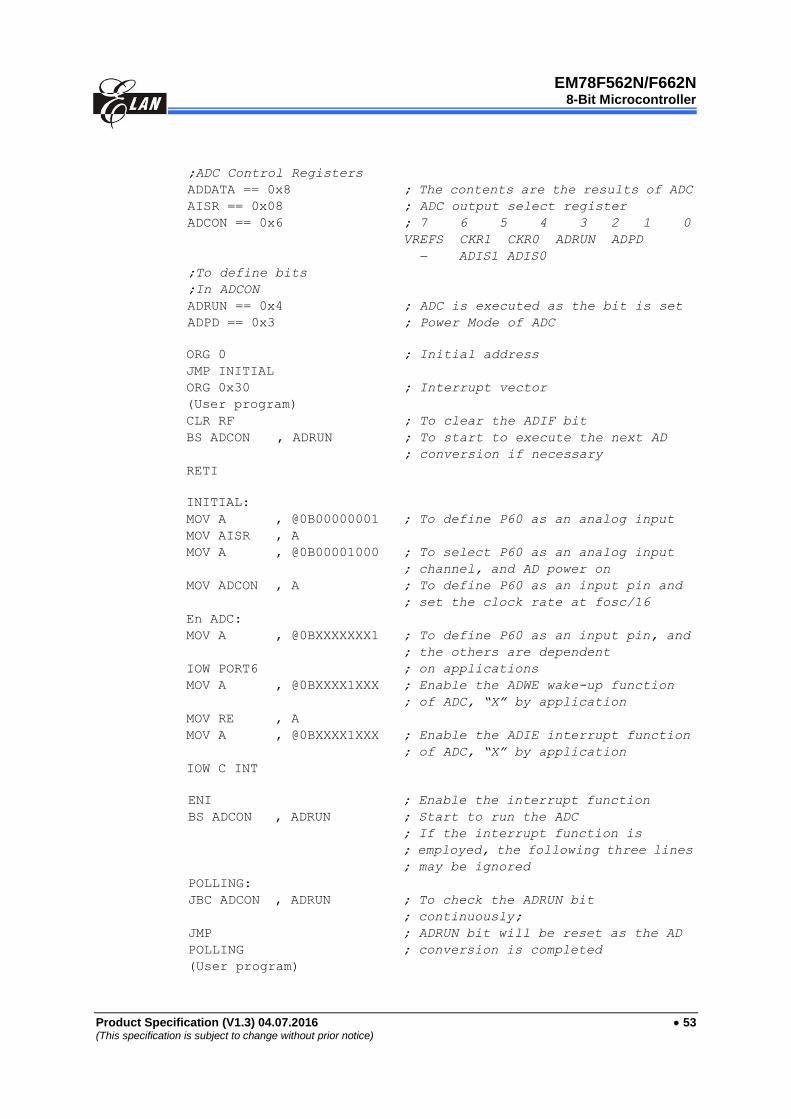
EM78F562N/F662N
8-Bit Microcontroller
Product Specification (V1.3) 04.07.2016 53 (This specification is subject to change without prior notice)
;ADC Control Registers ADDATA == 0x8 ; The contents are the results of ADC
AISR == 0x08 ; ADC output select register
ADCON == 0x6 ; 7 6 5 4 3 2 1 0
VREFS CKR1 CKR0 ADRUN ADPD
ADIS1 ADIS0
;To define bits
;In ADCON
ADRUN == 0x4 ; ADC is executed as the bit is set
ADPD == 0x3 ; Power Mode of ADC
ORG 0 ; Initial address
JMP INITIAL
ORG 0x30 ; Interrupt vector
(User program)
CLR RF ; To clear the ADIF bit
BS ADCON , ADRUN ; To start to execute the next AD
; conversion if necessary
RETI
INITIAL:
MOV A , @0B00000001 ; To define P60 as an analog input
MOV AISR , A
MOV A , @0B00001000 ; To select P60 as an analog input
; channel, and AD power on
MOV ADCON , A ; To define P60 as an input pin and
; set the clock rate at fosc/16
En_ADC:
MOV A , @0BXXXXXXX1 ; To define P60 as an input pin, and
; the others are dependent
IOW PORT6 ; on applications
MOV A , @0BXXXX1XXX ; Enable the ADWE wake-up function
; of ADC, “X” by application
MOV RE , A
MOV A , @0BXXXX1XXX ; Enable the ADIE interrupt function
; of ADC, “X” by application
IOW C_INT
ENI ; Enable the interrupt function
BS ADCON , ADRUN ; Start to run the ADC
; If the interrupt function is
; employed, the following three lines
; may be ignored
POLLING:
JBC ADCON , ADRUN ; To check the ADRUN bit
; continuously;
JMP
POLLING
; ADRUN bit will be reset as the AD
; conversion is completed
(User program)

EM78F562N/F662N
8-Bit Microcontroller
54 Product Specification (V1.3) 04.07.2016
(This specification is subject to change without prior notice)
6.9 Timer/Counter 2
16-bit Up-counter
Comparator
TCR2HTC2CR
M
TC2ES
TC2 Pin
TC2CK TC2S3
TC2 Interrupt
TCR2L
fc/223
fc/213
fc/28
Clear
Window
MUX
fc/23
fc
Figure 6-19 Timer / Counter 2 Configuration
In Timer mode, counting up is performed using the internal clock. When the contents
of the up-counter match the TCR2 (TCR2H+TCR2L), interrupt is generated and the
counter is cleared. Counting up resumes after the counter is cleared.
0 1 2 4 n-1 n 1 2 3
Internal clock
Up-counter 5
TC2 interrupt
0
n
match counter clear
TCR2
n-2n-33
Figure 6-20 Timer Mode Timing Chart
In Counter mode, counting up is performed using external clock input pin (TC2 pin)
and either rising or falling can be selected by setting TC2ES. When the contents of the
up-counter match the TCR2 (TCR2H+TCR2L), interrupt is generated and the counter
is cleared. Counting up resumes after the counter is cleared.

EM78F562N/F662N
8-Bit Microcontroller
Product Specification (V1.3) 04.07.2016 55 (This specification is subject to change without prior notice)
0 1 2 3 n-1 n 1 2 3
TC2 Pin
Up-counter 4
TC2 interrupt
0
n
match counter clear
TCR2
n-2
Figure 6-21 Counter Mode Timing Chart (INT2ES = 1)
In Window mode, counting up is performed on a rising edge of the pulse that is logical
AND of an internal clock and the TC2 pin (window pulse). When the contents of the
up-counter match the TCR2 (TCR2H+TCR2L), interrupt is generated and the counter
is cleared. The frequency (window pulse) must be slower than the selected internal
clock.
While writing to the TCR2L, comparison is inhibited until TCR2H is written.
0 1 2 n-3 n-1 n 1 2 3
Internal Clock
Up-counter n-2
TC2 Pin
TC2 Interrupt
0
n
match counter clear
TCR2
Figure 6-22 Window Mode Timing Chart

EM78F562N/F662N
8-Bit Microcontroller
56 Product Specification (V1.3) 04.07.2016
(This specification is subject to change without prior notice)
6.10 Timer/Counter 3
Figure 6-23 Timer / Counter 3 Configuration
In Timer mode, counting up is performed using the internal clock (rising edge trigger).
When the contents of the up-counter match the contents of TCR3, interrupt is
generated and the counter is cleared. Counting up resumes after the counter is
cleared.
In Counter mode, counting up is performed using the external clock input pin (TC3
pin). When the contents of the up-counter match the contents of TCR3, interrupt is
generated and the counter is cleared. Counting up resumes after the counter is
cleared.
In Programmable Divider Output (PDO) mode, counting up is performed using the
internal clock. The contents of TCR3 are compared with the contents of the up-counter.
The F/F output is toggled and the counter is cleared each time a match is found. The
F/F output is inverted and output to /PDO pin. This mode can generate 50% duty pulse
output. The F/F can be initialized by the program and it is initialized to “0” during
reset. A TC3 interrupt is generated each time the /PDO output is toggled.
0 1 3 n-1 n 0 n-1 n 0 1 n-1 0 1 2
Source Clock
Up-counter
TCR3
TC3 Interrupt
n
2 1 n
F/F
/PDO Pin
Figure 6-24 PDO Mode Timing Chart

EM78F562N/F662N
8-Bit Microcontroller
Product Specification (V1.3) 04.07.2016 57 (This specification is subject to change without prior notice)
In Pulse Width Modulation (PWM) Output mode, counting up is performed using the
internal clock. The contents of TCR3 are compared with the contents of the up-counter.
The F/F is toggled when a match is found. While the counter is counting, the F/F is
toggled again when the counter overflows, then the counter is cleared. The F/F output
is inverted and output to the /PWM pin. A TC3 interrupt is generated each time an
overflow occurs. TCR3 is configured as a 2-stage shift register and during output,
will not switch until one output cycle is completed even if TCR3 is overwritten.
Hence, the output can be changed continuously. Also, on the first time, TRC3 is shifted
by setting TC3S to “1” after data is loaded to TCR3.
0 1 n-1 n n+1 FE FF 0 n+1 FE FF 0
Source Clock
Up-counter
TCR3
TC4 Interrupt
n/n
n+2
F/F
/PWM
match overflow
n-1 n
match
n+2
overflow
1 period
n/m m/m
overwrite Shift
m-11 m
Figure 6-25 PWM Mode Timing Chart
6.11 Comparator
The EM78F562N/F662N has one comparator comprising of two analog inputs and one
output. The comparator can be utilized to wake up the EM78F562N/F662N from sleep
mode. The comparator circuit diagram is depicted in the figure below.
CMPOUT
CMP+
CMP-
Comparator
CPS1 CPS0
Figure 6-26 Comparator Block Diagram
NOTE
The reference signal must be between Vss and Vdd.
The reference voltage can be applied to either pin of the comparator.
Threshold detector applications may be of the same reference.
The comparator can operate from the same or different reference sources.
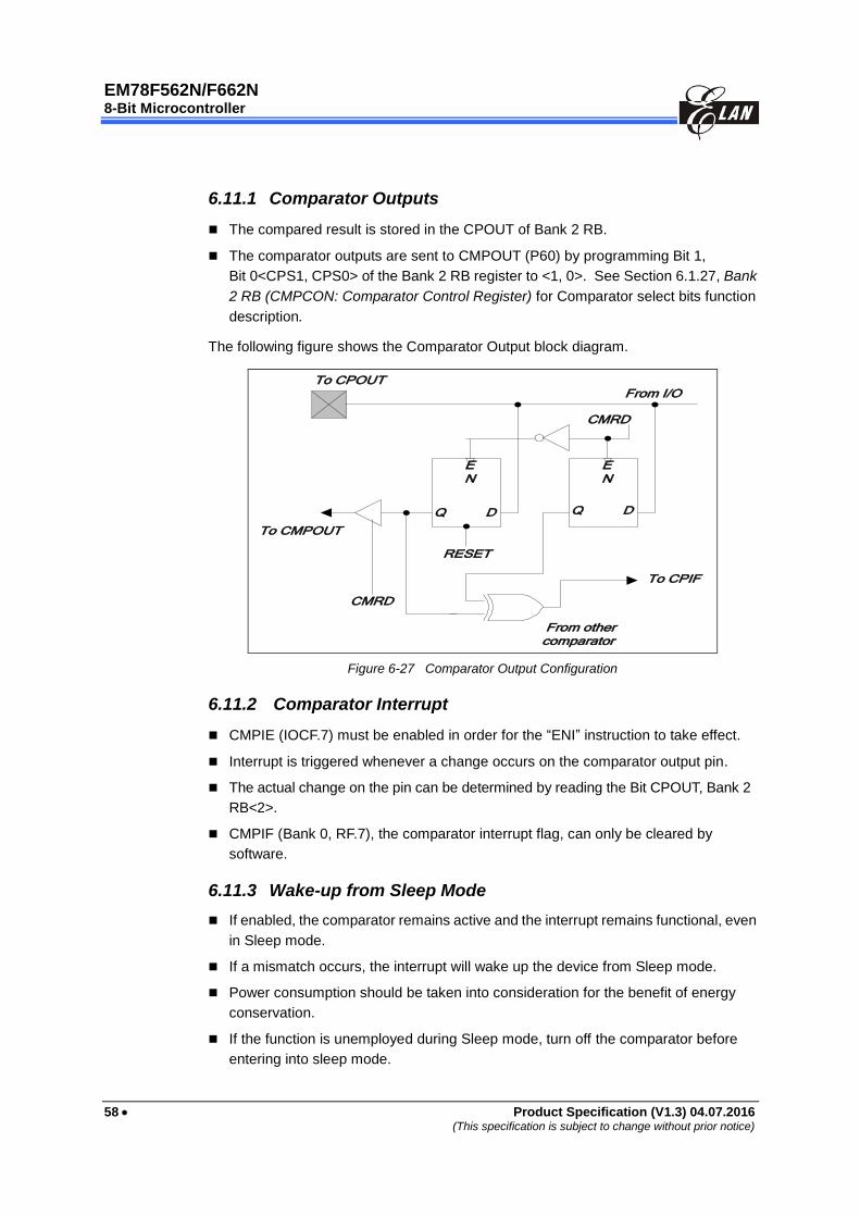
EM78F562N/F662N
8-Bit Microcontroller
58 Product Specification (V1.3) 04.07.2016
(This specification is subject to change without prior notice)
6.11.1 Comparator Outputs
The compared result is stored in the CPOUT of Bank 2 RB.
The comparator outputs are sent to CMPOUT (P60) by programming Bit 1,
Bit 0<CPS1, CPS0> of the Bank 2 RB register to <1, 0>. See Section 6.1.27, Bank
2 RB (CMPCON: Comparator Control Register) for Comparator select bits function
description.
The following figure shows the Comparator Output block diagram.
Q Q
EN
EN
DD
To CPOUT
To CPIF
To CMPOUT
CMRD
CMRD
From othercomparator
RESET
From I/O
Figure 6-27 Comparator Output Configuration
6.11.2 Comparator Interrupt
CMPIE (IOCF.7) must be enabled in order for the “ENI” instruction to take effect.
Interrupt is triggered whenever a change occurs on the comparator output pin.
The actual change on the pin can be determined by reading the Bit CPOUT, Bank 2
RB<2>.
CMPIF (Bank 0, RF.7), the comparator interrupt flag, can only be cleared by
software.
6.11.3 Wake-up from Sleep Mode
If enabled, the comparator remains active and the interrupt remains functional, even
in Sleep mode.
If a mismatch occurs, the interrupt will wake up the device from Sleep mode.
Power consumption should be taken into consideration for the benefit of energy
conservation.
If the function is unemployed during Sleep mode, turn off the comparator before
entering into sleep mode.

EM78F562N/F662N
8-Bit Microcontroller
Product Specification (V1.3) 04.07.2016 59 (This specification is subject to change without prior notice)
6.12 Oscillator
6.12.1 Oscillator Modes
The device can be operated in four different oscillator modes, such as Internal RC
oscillator mode (IRC), External RC oscillator mode (ERC), High Crystal oscillator mode
(HXT), and Low Crystal oscillator mode (LXT). User can select one of such modes by
programming OSC2, OCS1 and OSC0 in the Code Option register. Table 6-6 depicts
how these four modes are defined.
The up-limited operation frequency of the crystal/resonator on the different VDD is
listed in Table 6-7:
Table 6-6 Oscillator Modes defined by OSC2 ~ OSC0
Mode OSC2 OSC1 OSC0
XT (Crystal oscillator mode) 0 0 0
HXT (High Crystal oscillator mode) 0 0 1
LXT1 (Low Crystal 1 oscillator mode) 0 1 0
LXT2 (Low Crystal 2 oscillator mode) 0 1 1
IRC mode, OSCO (P54) act as I/O pin 1 0 0
IRC mode, OSCO (P54) act as RCOUT pin 1 0 1
ERC mode, OSCO (P54) act as I/O pin 1 1 0
ERC mode, OSCO (P54) act as RCOUT pin 1 1 1
Note: 1. The Frequency range of the HXT mode is 16 MHz ~ 6 MHz.
2. The Frequency range of the XT mode is 6 MHz ~ 1 MHz.
3. The Frequency range of the LXT1 mode is 1 MHz ~ 100kHz.
4. The Frequency range of the LXT2 mode is 32kHz.
In LXT, XT, HXT and ERC mode, OSCI and OSCO are implemented but they cannot
be used as normal I/O pins.
In IRC mode, P55 is used as normal I/O pin.
Table 6-7 Summary of Maximum Operating Speeds
Conditions VDD Max. Fxt. (MHz)
Two cycles with two clocks
2.5 4.0
3.0 8.0
5.0 20.0

EM78F562N/F662N
8-Bit Microcontroller
60 Product Specification (V1.3) 04.07.2016
(This specification is subject to change without prior notice)
6.12.2 Crystal Oscillator/Ceramic Resonators (Crystal)
The EM78F562N/F662N can be driven by an external clock signal through the OSCI
pin as shown in Figure 6-28 below.
OSCI
OSCO
Ext. Clock
Figure 6-28 Circuit for External Clock Input
In most applications, pin OSCI and pin OSCO can be connected with a crystal or
ceramic resonator to generate oscillation. Figure 6-29 depicts such a circuit. The
same thing applies whether it is in the HXT mode or in the LXT mode. Table 6-8
provides the recommended values for C1 and C2. Since each resonator has its own
attribute, user should refer to its specification for appropriate values of C1 and C2. RS,
a serial resistor, may be necessary for AT strip cut crystal or low frequency mode.
OSCI
OSCO
C1
C2
Crystal
RS
Figure 6-29 Circuit for Crystal/Resonator
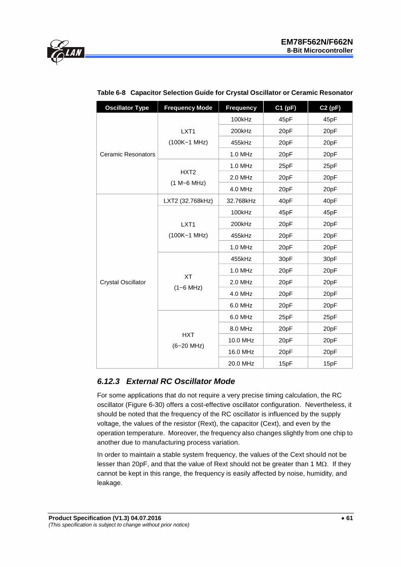
EM78F562N/F662N
8-Bit Microcontroller
Product Specification (V1.3) 04.07.2016 61 (This specification is subject to change without prior notice)
Table 6-8 Capacitor Selection Guide for Crystal Oscillator or Ceramic Resonator
Oscillator Type Frequency Mode Frequency C1 (pF) C2 (pF)
Ceramic Resonators
LXT1
(100K~1 MHz)
100kHz 45pF 45pF
200kHz 20pF 20pF
455kHz 20pF 20pF
1.0 MHz 20pF 20pF
HXT2
(1 M~6 MHz)
1.0 MHz 25pF 25pF
2.0 MHz 20pF 20pF
4.0 MHz 20pF 20pF
Crystal Oscillator
LXT2 (32.768kHz) 32.768kHz 40pF 40pF
LXT1
(100K~1 MHz)
100kHz 45pF 45pF
200kHz 20pF 20pF
455kHz 20pF 20pF
1.0 MHz 20pF 20pF
XT
(1~6 MHz)
455kHz 30pF 30pF
1.0 MHz 20pF 20pF
2.0 MHz 20pF 20pF
4.0 MHz 20pF 20pF
6.0 MHz 20pF 20pF
HXT
(6~20 MHz)
6.0 MHz 25pF 25pF
8.0 MHz 20pF 20pF
10.0 MHz 20pF 20pF
16.0 MHz 20pF 20pF
20.0 MHz 15pF 15pF
6.12.3 External RC Oscillator Mode
For some applications that do not require a very precise timing calculation, the RC
oscillator (Figure 6-30) offers a cost-effective oscillator configuration. Nevertheless, it
should be noted that the frequency of the RC oscillator is influenced by the supply
voltage, the values of the resistor (Rext), the capacitor (Cext), and even by the
operation temperature. Moreover, the frequency also changes slightly from one chip to
another due to manufacturing process variation.
In order to maintain a stable system frequency, the values of the Cext should not be
lesser than 20pF, and that the value of Rext should not be greater than 1 M. If they
cannot be kept in this range, the frequency is easily affected by noise, humidity, and
leakage.

EM78F562N/F662N
8-Bit Microcontroller
62 Product Specification (V1.3) 04.07.2016
(This specification is subject to change without prior notice)
The smaller the Rext in the RC oscillator, the faster its frequency will be. On the
contrary, for very low Rext values, for instance, 1 K, the oscillator becomes unstable
since the NMOS cannot discharge correctly the current of the capacitance.
Based on the above reasons, it must be kept in mind that the supply voltage, the
operation temperature, the components of the RC oscillator, the package types, and
the PCB layout, will affect the system frequency.
ERCin
EM78F662N
Vcc
Rext
Cext
Figure 6-30 Circuit for External RC Oscillator Mode
Table 6-9 RC Oscillator Frequencies
Cext Rext Average Fosc 5V, 25C Average Fosc 3V, 25C
20 pF
3.3k 3.5 MHz 3.2 MHz
5.1k 2.5 MHz 2.3 MHz
10k 1.30 MHz 1.25 MHz
100k 140kHz 140kHz
100 pF
3.3k 1.27 MHz 1.21 MHz
5.1k 850kHz 820kHz
10k 450kHz 450kHz
100k 48kHz 50kHz
300 pF
3.3k 560kHz 540kHz
5.1k 370kHz 360kHz
10k 196kHz 192kHz
100k 20kHz 20kHz
Note: 1: These are measured based on DIP packages.
2: These values are for design reference only. Actual values may vary depending on the
actual process.

EM78F562N/F662N
8-Bit Microcontroller
Product Specification (V1.3) 04.07.2016 63 (This specification is subject to change without prior notice)
6.12.4 Internal RC Oscillator Mode
Table 6-10 Internal RC Drift Rate (Ta=25C, VDD=5 V± 5%, VSS=0V)
Internal RC
Drift Rate
Temperature
(-40C~85C)
Voltage
(2.2V~5.5V) Process Total
1 MHz ± 3% ± 4% ± 2.5% ± 9.5%
4 MHz ± 3% ± 4% ± 2.5% ± 9.5%
8 MHz ± 3% ± 5% ± 2.5% ± 10.5%
16 MHz ± 3% ± 5% ± 2.5% ± 10.5%
6.13 Code Option Register
The EM78F562N/F662N has a Code option word that is not part of the normal program
memory. The option bits cannot be accessed during normal program execution.
Code Option Register and Customer ID Register arrangement distribution:
Word 0 Word 1 Word 2
Bit 12~Bit 0 Bit 12~Bit 0 Bit 12~Bit 0
6.13.1 Code Option Register (Word 0)
Word 0
Bit Bit 12 Bit 11 Bit 10 Bit 9 Bit 8 Bit 7 Bit 6 Bit 5 Bit 4 Bit 3 Bit 2 Bit 1 Bit 0
Mnemonic - NRHL NRE RESETENB CLKS1 CLKS0 ENWDTB OSC2 OSC1 OSC0 PR2 PR1 PR0
1 - 8/fc Disable Enable High High Enable High High High High High High
0 - 32/fc Enable Disable Low Low Disable Low Low Low Low Low Low
Bit 12: Not used, always set to “0”.
Bit 11 (NRHL): Noise rejection high/low pulse defined bit. The INT pin is a falling edge
trigger.
1 : Pulses equal to 8/fc [s] are regarded as signal
0 : Pulses equal to 32/fc [s] are regarded as signal (default)
NOTE
The noise rejection function is turned off in the LXT2 and sleep mode.
Bit 10 (NRE): Noise rejection enable (depends on EM78F562N/F662N). The INT pin
is a falling edge trigger.
1 : Disable noise rejection
0 : Enable noise rejection (default) but in Low Crystal oscillator (LXT)
mode, the noise rejection circuit is always disabled
Bit 9 (RESETENB): Reset Pin Enable Bit

EM78F562N/F662N
8-Bit Microcontroller
64 Product Specification (V1.3) 04.07.2016
(This specification is subject to change without prior notice)
0 : Disable, P83//RESET P83 (default)
1 : Enable, P83//RESET RESET pin
Bit 8 ~ Bit 7 (CLKS1 ~ CLKS0): Instruction period option bit
Instruction Period CLKS1 CLKS0
4 clocks 0 0
2 clocks 0 1
8 clocks 1 0
16 clocks 1 1
Refer to the Instruction Set section.
Bit 6 (ENWDTB): Watchdog timer enable bit
0 : Disable
1 : Enable
Bit 5 ~ Bit 3 (OSC2 ~ OSC0): Oscillator Mode Select bits
Oscillator Modes defined by OSC2 ~ OSC0
Mode OSC2 OSC1 OSC0
XT (Crystal oscillator mode) 0 0 0
HXT (High Crystal oscillator mode) 0 0 1
LXT1 (Low Crystal 1 oscillator mode) 0 1 0
LXT2 (Low Crystal 2 oscillator mode) 0 1 1
IRC mode, OSCO (P54) act as I/O pin 1 0 0
IRC mode, OSCO (P54) act as RCOUT pin 1 0 1
ERC mode, OSCO (P54) act as I/O pin 1 1 0
ERC mode, OSCO (P54) act as RCOUT pin 1 1 1
Note: 1. Frequency range of HXT mode is 16 MHz ~ 6 MHz.
2. Frequency range of XT mode is 6 MHz ~ 1 MHz.
3. Frequency range of LXT1 mode is 1 MHz ~ 100kHz.
4. Frequency range of LXT2 mode is 32kHz.
Bit 2 ~ Bit 0 (PR2 ~ PR0): Protect Bits. Protect type is as follows:
PR2 PR1 PR0 Protect
1 1 1 Enable
0 0 0 Disable
6.13.2 Code Option Register (Word 1)
Word 1
Bit Bit 12 Bit 11 Bit 10 Bit 9 Bit 8 Bit 7 Bit 6 Bit 5 Bit 4 Bit 3 Bit 2 Bit 1 Bit 0
Mnemonic COBS TCEN - - C4 C3 C2 C1 C0 RCM1 RCM0 LVR1 LVR0
1 High TCC - - High High High High High High High High High
0 Low P77 - - Low Low Low Low Low Low Low Low Low
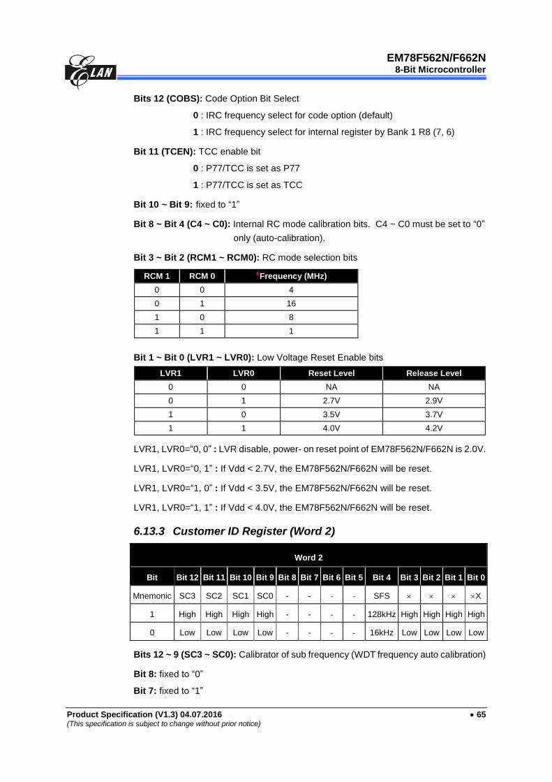
EM78F562N/F662N
8-Bit Microcontroller
Product Specification (V1.3) 04.07.2016 65 (This specification is subject to change without prior notice)
Bits 12 (COBS): Code Option Bit Select
0 : IRC frequency select for code option (default)
1 : IRC frequency select for internal register by Bank 1 R8 (7, 6)
Bit 11 (TCEN): TCC enable bit
0 : P77/TCC is set as P77
1 : P77/TCC is set as TCC
Bit 10 ~ Bit 9: fixed to “1”
Bit 8 ~ Bit 4 (C4 ~ C0): Internal RC mode calibration bits. C4 ~ C0 must be set to “0”
only (auto-calibration).
Bit 3 ~ Bit 2 (RCM1 ~ RCM0): RC mode selection bits
RCM 1 RCM 0 *Frequency (MHz)
0 0 4
0 1 16
1 0 8
1 1 1
Bit 1 ~ Bit 0 (LVR1 ~ LVR0): Low Voltage Reset Enable bits
LVR1 LVR0 Reset Level Release Level
0 0 NA NA
0 1 2.7V 2.9V
1 0 3.5V 3.7V
1 1 4.0V 4.2V
LVR1, LVR0=“0, 0” : LVR disable, power- on reset point of EM78F562N/F662N is 2.0V.
LVR1, LVR0=“0, 1” : If Vdd < 2.7V, the EM78F562N/F662N will be reset.
LVR1, LVR0=“1, 0” : If Vdd < 3.5V, the EM78F562N/F662N will be reset.
LVR1, LVR0=“1, 1” : If Vdd < 4.0V, the EM78F562N/F662N will be reset.
6.13.3 Customer ID Register (Word 2)
Word 2
Bit Bit 12 Bit 11 Bit 10 Bit 9 Bit 8 Bit 7 Bit 6 Bit 5 Bit 4 Bit 3 Bit 2 Bit 1 Bit 0
Mnemonic SC3 SC2 SC1 SC0 - - - - SFS X
1 High High High High - - - - 128kHz High High High High
0 Low Low Low Low - - - - 16kHz Low Low Low Low
Bits 12 ~ 9 (SC3 ~ SC0): Calibrator of sub frequency (WDT frequency auto calibration)
Bit 8: fixed to “0”
Bit 7: fixed to “1”

EM78F562N/F662N
8-Bit Microcontroller
66 Product Specification (V1.3) 04.07.2016
(This specification is subject to change without prior notice)
Bits 6 ~ 5: fixed to “0”
Bit 4 (SFS): Sub Frequency Select
0: 16kHz (WDT frequency)
1: 128kHz
Bits 3 ~ 0: Customer’s ID code
6.14 Power-on Considerations
Any microcontroller is not guaranteed to start to operate properly before the power
supply has stabilized. The EM78F562N/F662N has an on-chip Power-on Voltage
Detector (POVD) with a detecting level of 2.0V. It will work well if Vdd can rise quickly
enough (50ms or less). In many critical applications, however, extra devices are still
required to assist in solving power-up problems.
6.15 External Power-on Reset Circuit
The circuit shown in Figure 6-31 uses an external RC to produce a reset pulse. The
pulse width (time constant) should be kept long enough for Vdd to reached minimum
operating voltage. This circuit is used when the power supply has a slow rise time.
Because the current leakage from the /RESET pin is 5 A, it is recommended that R
should not be greater than 40K. In this way, the /RESET pin voltage is held below 0.2V.
The diode (D) functions as a short circuit at the moment of power down.
The capacitor C will discharge rapidly and fully. The current-limited resistor (Rin), will
prevent high current or ESD (electrostatic discharge) from flowing to Pin /RESET.
/RESET
Vdd
D
R
Rin C
Figure 6-31 External Power-up Reset Circuit
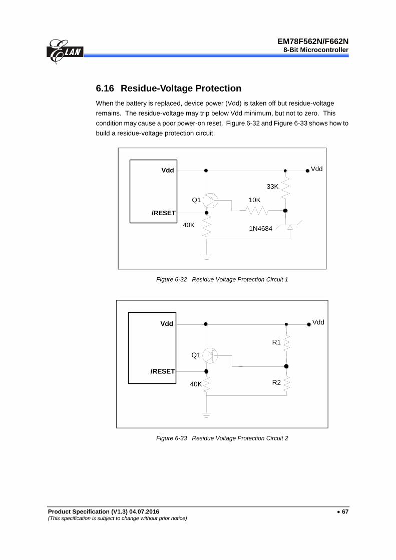
EM78F562N/F662N
8-Bit Microcontroller
Product Specification (V1.3) 04.07.2016 67 (This specification is subject to change without prior notice)
6.16 Residue-Voltage Protection
When the battery is replaced, device power (Vdd) is taken off but residue-voltage
remains. The residue-voltage may trip below Vdd minimum, but not to zero. This
condition may cause a poor power-on reset. Figure 6-32 and Figure 6-33 shows how to
build a residue-voltage protection circuit.
/RESET
Vdd
40K
Q1
1N4684
10K
33K
Vdd
Figure 6-32 Residue Voltage Protection Circuit 1
/RESET
Vdd
Q1
Vdd
40K R2
R1
Figure 6-33 Residue Voltage Protection Circuit 2

EM78F562N/F662N
8-Bit Microcontroller
68 Product Specification (V1.3) 04.07.2016
(This specification is subject to change without prior notice)
6.17 Instruction Set
Each instruction in the instruction set is a 13-bit word divided into an OP code and one
or more operands. Normally, all instructions are executed within one single instruction
cycle (one instruction consists of two oscillator periods), unless the program counter is
changed by instruction "MOV R2,A", "ADD R2,A", or by instructions of arithmetic or
logic operation on R2 (e.g. "SUB R2,A", "BS(C) R2,6", "CLR R2", etc.). In this case, the
execution takes two instruction cycles.
If for some reasons, the specification of the instruction cycle is not suitable for certain
applications, try to modify the instructions as follows:
(A) Change one instruction cycle to consist of four oscillator periods.
(B) "JMP", "CALL", "RET", "RETL", "RETI" commands are executed with one
instruction cycle, the conditional skip ("JBS", "JBC", "JZ", "JZA", "DJZ", "DJZA")
commands which were tested to be true, are executed within two instruction
cycles. The instructions that are written to the program counter also take two
instruction cycles.
Case (A) is selected by the Code Option bit, called CLK. One instruction cycle
consists of two oscillator clocks if CLK is low and four oscillator clocks if CLK is
high.
Note that once the four oscillator periods within one instruction cycle is selected as
in Case (A), the internal clock source to TCC should be CLK=Fosc/4, instead of
Fosc / 2 as indicated in Figure 6-11.
In addition, the instruction set has the following features:
(1) Every bit of any register can be set, cleared, or tested directly.
(2) The I/O register can be regarded as general register. That is, the same instruction
can operate on the I/O register.
Instruction Set Convention:
R = Register designator that specifies which one of the registers (including operation and general
purpose registers) is to be utilized by the instruction.
b = Bit field designator that selects the value for the bit located in the register R and which affects
the operation.
k = 8 or 10-bit constant or literal value

EM78F562N/F662N
8-Bit Microcontroller
Product Specification (V1.3) 04.07.2016 69 (This specification is subject to change without prior notice)
Mnemonic Operation Status Affected
NOP No Operation None
DAA Decimal Adjust A C
CONTW A CONT None
SLEP 0 WDT, Stop oscillator T, P
WDTC 0 WDT T, P
IOW R A IOCR None 1
ENI Enable Interrupt None
DISI Disable Interrupt None
RET [Top of Stack] PC None
RETI [Top of Stack] PC, Enable Interrupt
None
CONTR CONT A None
IOR R IOCR A None 1
MOV R,A A R None
CLRA 0 A Z
CLR R 0 R Z
SUB A,R R-A A Z, C, DC
SUB R,A R-A R Z, C, DC
DECA R R-1 A Z
DEC R R-1 R Z
OR A,R A R A Z
OR R,A A R R Z
AND A,R A & R A Z
AND R,A A & R R Z
XOR A,R A R A Z
XOR R,A A R R Z
ADD A,R A + R A Z, C, DC
ADD R,A A + R R Z, C, DC
MOV A,R R A Z
MOV R,R R R Z
COMA R /R A Z
COM R /R R Z
INCA R R+1 A Z
INC R R+1 R Z
Note: 1
This instruction is applicable to IOC5~IOC7, IOCA ~ IOCF only.
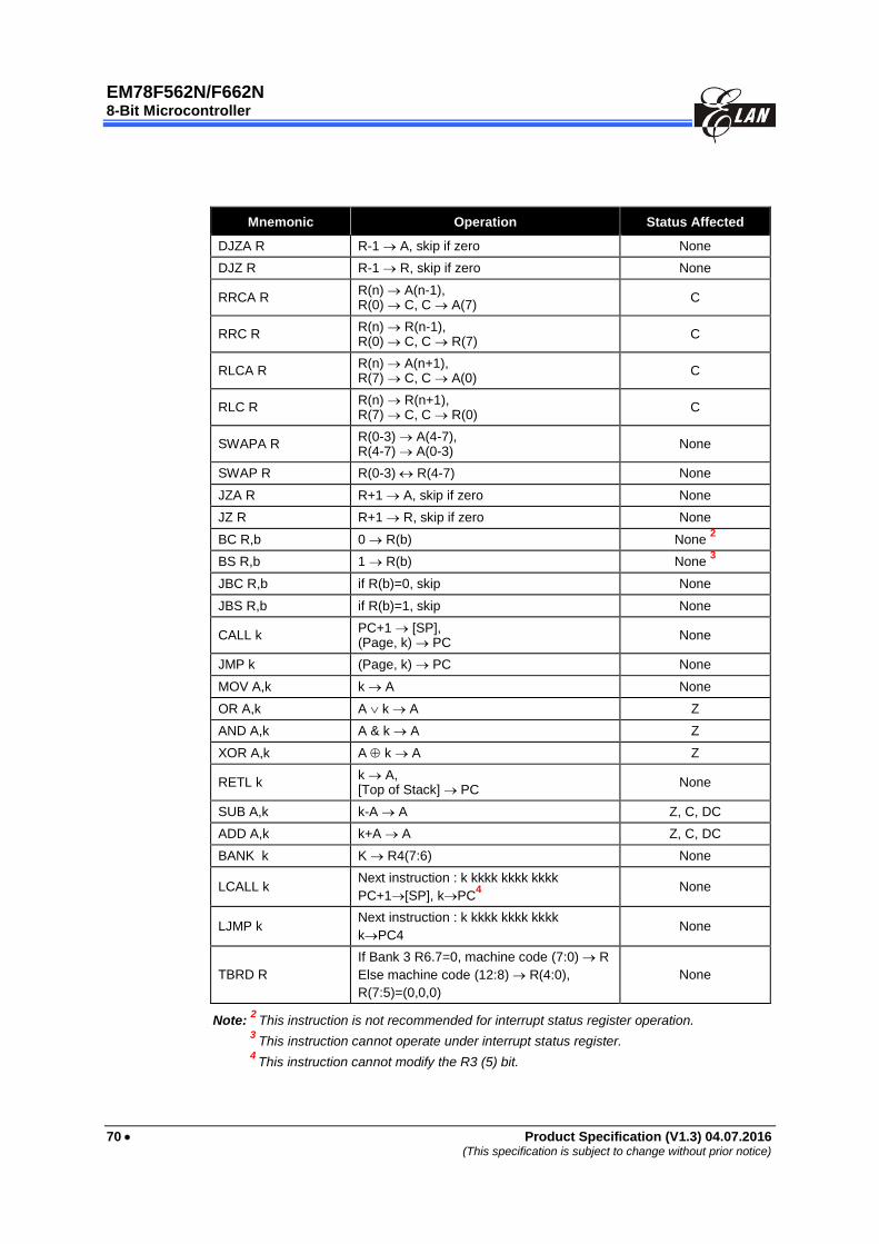
EM78F562N/F662N
8-Bit Microcontroller
70 Product Specification (V1.3) 04.07.2016
(This specification is subject to change without prior notice)
Mnemonic Operation Status Affected
DJZA R R-1 A, skip if zero None
DJZ R R-1 R, skip if zero None
RRCA R R(n) A(n-1), R(0) C, C A(7)
C
RRC R R(n) R(n-1), R(0) C, C R(7)
C
RLCA R R(n) A(n+1), R(7) C, C A(0)
C
RLC R R(n) R(n+1), R(7) C, C R(0)
C
SWAPA R R(0-3) A(4-7), R(4-7) A(0-3)
None
SWAP R R(0-3) R(4-7) None
JZA R R+1 A, skip if zero None
JZ R R+1 R, skip if zero None
BC R,b 0 R(b) None 2
BS R,b 1 R(b) None 3
JBC R,b if R(b)=0, skip None
JBS R,b if R(b)=1, skip None
CALL k PC+1 [SP], (Page, k) PC
None
JMP k (Page, k) PC None
MOV A,k k A None
OR A,k A k A Z
AND A,k A & k A Z
XOR A,k A k A Z
RETL k k A, [Top of Stack] PC
None
SUB A,k k-A A Z, C, DC
ADD A,k k+A A Z, C, DC
BANK k K R4(7:6) None
LCALL k Next instruction : k kkkk kkkk kkkk
PC+1[SP], kPC4
None
LJMP k Next instruction : k kkkk kkkk kkkk
kPC4 None
TBRD R
If Bank 3 R6.7=0, machine code (7:0) R
Else machine code (12:8) R(4:0),
R(7:5)=(0,0,0)
None
Note: 2
This instruction is not recommended for interrupt status register operation. 3
This instruction cannot operate under interrupt status register. 4
This instruction cannot modify the R3 (5) bit.
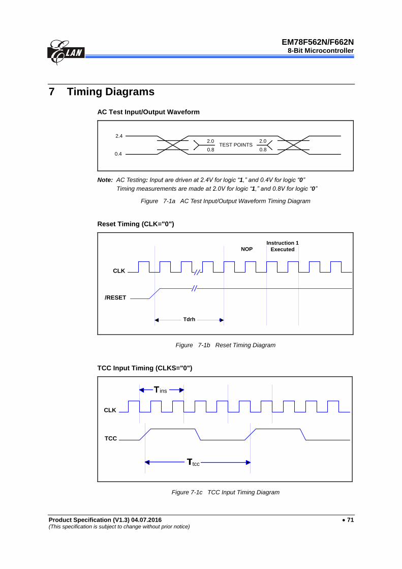
EM78F562N/F662N
8-Bit Microcontroller
Product Specification (V1.3) 04.07.2016 71 (This specification is subject to change without prior notice)
7 Timing Diagrams
AC Test Input/Output Waveform
0.4
TEST POINTS
2.42.0
0.8
2.0
0.8
Note: AC Testing: Input are driven at 2.4V for logic “1,” and 0.4V for logic “0”
Timing measurements are made at 2.0V for logic “1,” and 0.8V for logic “0”
Figure 7-1a AC Test Input/Output Waveform Timing Diagram
Reset Timing (CLK="0")
NOPInstruction 1
Executed
Tdrh
CLK
/RESET
Figure 7-1b Reset Timing Diagram
TCC Input Timing (CLKS="0")
ins
tcc
CLK
TCC
Figure 7-1c TCC Input Timing Diagram

EM78F562N/F662N
8-Bit Microcontroller
72 Product Specification (V1.3) 04.07.2016
(This specification is subject to change without prior notice)
8 Absolute Maximum Ratings
EM78F562N/F662N
Items Rating
Temperature under bias -40C to 85C
Storage temperature -65C to 150C
Working voltage 2.2 to 5.5V
Working frequency DC to 20 MHz
Input voltage Vss-0.3V to Vdd+0.5V
Output voltage Vss-0.3V to Vdd+0.5V
Note: These parameters are theoretical values and have not been tested.
9 DC Electrical Characteristics
(Ta=25C, VDD=5.0V5%, VSS=0V)
Symbol Parameter Condition Min. Typ. Max. Unit
Fxt
Crystal: VDD to 3V Two cycles with two clocks
DC - 8 MHz
Crystal: VDD to 5V DC - 20 MHz
ERC: VDD to 5V R: 5.1K, C: 100 pF F30 830 F30 kHz
IRC: VDD to 5V 4MHz, 16MHz, 8MHz, 1MHz F30 F F30 Hz
IIL Input Leakage Current for input pins VIN = VDD, VSS - - 1 µA
VIHRC Input High Threshold Voltage (Schmitt trigger)
OSCI in RC mode 3.9 4 4.1 V
IERC1 Sink current VI from low to high , VI=5V 21 22 23 mA
VILRC Input Low Threshold Voltage (Schmitt trigger)
OSCI in RC mode 1.7 1.8 1.9 V
IERC2 Sink current VI from high to low , VI=2V 16 17 18 mA
IIL Input Leakage Current for input pins VIN = VDD, VSS -1 0 1 µA
VIH1 Input High Voltage (Schmitt trigger) Ports 5, 6, 7, 8 - 0.7VDD - V
VIL1 Input Low Voltage (Schmitt trigger) Ports 5, 6, 7, 8 - 0.3VDD - V
VIHT1 Input High Threshold Voltage (Schmitt trigger)
/RESET - 0.7VDD - V
VILT1 Input Low Threshold Voltage (Schmitt trigger)
/RESET - 0.3VDD - V
VIHT2 Input High Threshold Voltage (Schmitt trigger)
TCC, INT - 0.7VDD - V
VILT2 Input Low Threshold Voltage (Schmitt trigger)
TCC, INT - 0.3VDD - V
VIHX1 Clock Input High Voltage OSCI in crystal mode 2.9 3.0 3.1 V
VILX1 Clock Input Low Voltage OSCI in crystal mode 1.7 1.8 1.9 V
IOH1 Output High Voltage (Ports 5, 6, 7, 8)
VOH = 0.9VDD -3 - - mA
IOL1 Output Low Voltage (Ports 5, 7, 8)
VOL = 0.1VDD 14 - - mA

EM78F562N/F662N
8-Bit Microcontroller
Product Specification (V1.3) 04.07.2016 73 (This specification is subject to change without prior notice)
Symbol Parameter Condition Min. Typ. Max. Unit
IOL2 Output Low Voltage (Ports 6) VOL = 0.1VDD - 18 - mA
LVR1 Low Voltage Reset level Ta= 25C 2.4 2.7 3.02 V
Ta= -40~85C 2.07 2.7 3.37 V
LVR2 Low Voltage Reset level Ta= 25C 3.09 3.5 3.98 V
Ta= -40~85C 2.58 3.5 4.46 V
LVR3 Low Voltage Reset level Ta= 25C 3.51 4.0 4.51 V
Ta= -40~85C 2.98 4.0 5.06 V
IPH Pull-high current Pull-high active, input pin at VSS - - -80 A
IPL Pull-low current Pull-low active, input pin at Vdd - - 30 A
ISB1 Power down current All input and I/O pins at VDD, output pin floating, WDT disabled
- 1.5 - A
ISB2 Power down current All input and I/O pins at VDD, output pin floating, WDT enabled
- 11 - A
ICC1 Operating supply current
at two clocks
/RESET= 'High', Fosc=32kHz (Crystal type), output pin floating, WDT disabled
- 43 - A
ICC2 Operating supply current
at two clocks
/RESET= 'High', Fosc=32kHz (Crystal type), output pin floating, WDT enabled
- 43 - A
ICC3 Operating supply current
at two clocks
/RESET= 'High', Fosc=4MHz (Crystal type), output pin floating, WDT enabled
- - 1 mA
ICC4 Operating supply current
at two clocks
/RESET= 'High', Fosc=10MHz (Crystal type), output pin floating, WDT enabled
- - 2.8 mA
ICC5 Operating supply current
at two clocks
/RESET= 'High', Fosc=1MHz (IRC type), Voltage = 3V, output pin floating, WDT enabled
- 180 - A
Note: These parameters are theoretical values and have not been tested nor verified.
Data in the Minimum, Typical, Maximum (”Min.”, “Typ.”, “Max.”) columns are based on
characterization results at 25°C. These data are for design reference only and have not been tested.
9.1 Data EEPROM Electrical Characteristics
Symbol Parameter Condition Min. Typ. Max. Unit
Tprog Erase/Write cycle time
Vdd = 2.4~ 5.5V
Temperature = -40 ~ 85C
- 4.5 - ms
Treten Data Retention - 10 - Years
Tendu Endurance time - 1000K - Cycles
Iprg Programming Vdd 3.3V - 0.6 - mA
Vdd 5.5V - 1.0 - mA
Iread Read Vdd 3.3V - 1.0 - mA
Vdd 5.5V - 2.5 - mA

EM78F562N/F662N
8-Bit Microcontroller
74 Product Specification (V1.3) 04.07.2016
(This specification is subject to change without prior notice)
9.2 Program Flash Memory Electrical Characteristics Symbol Parameter Condition Min. Typ. Max. Unit
Tprog Erase/Write cycle time Vdd = 5.0V
Temp. = -40~85C
- 4 - ms
Treten Data Retention - 10 - Years
Tendu Endurance time - 100K - Cycles
9.3 A/D Converter Characteristics
(Vdd=2.5V to 5.5V, Vss=0V, Ta=25C)
Symbol Parameter Condition Min. Typ. Max. Unit
VAREF Analog reference voltage
VAREF-VASS= 2.5V to
5.5V 2.5 Vss Vdd V
VASS
VAI Analog input voltage VASS VAREF V
IAI1 Ivdd VAREF = Vdd 1150 1300 1450 µA
Ivref -10 0 10 µA
IAI2 Ivdd VAREF = VREF 700 800 900 µA
Ivref 450 500 550 µA
RN Resolution VAREF=Vdd 8 9 Bits
LN Linearity error VAREF=Vdd 0 2 4 LSB
DNL Differential nonlinear
error VAREF=Vdd 0 0.5 0.9 LSB
FSE Full scale error VAREF=Vdd 0 1 2 LSB
OE Offset error VAREF=Vdd 0 1 2 LSB
ZAI
Recommended
impedance of analog
voltage source
VAREF=Vdd 0 8 10 K
TAD1 A/D clock period VAREF=Vdd=2.5~5.5V
Ta= -40~85C 4 µs
TAD2 A/D clock period VAREF=Vdd=3~5.5V
Ta= -40~85C 1 µs
TCN A/D conversion time VAREF=Vdd 14 14 TAD
PSR Power supply rejection Vdd=Vdd-10% to
Vdd+10% 0 2 LSB
Note: 1. These parameters are characterized but not tested.
2. These parameters are for design reference only and are not tested.
3. When A/D is off, there’s no current consumption other than minor leakage current.
4. The A/D conversion result does not decrease with an increase in the input voltage, and it has no missing code.
5. Specifications are subject to change without prior notice.
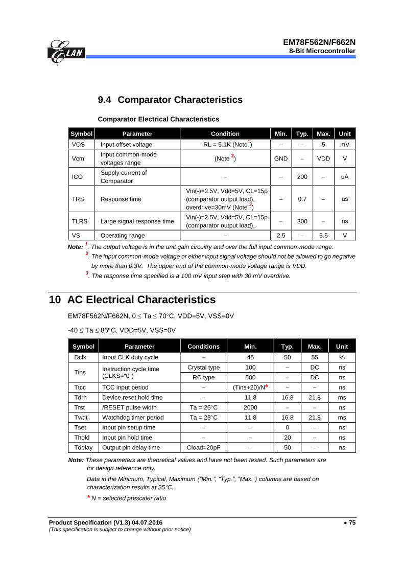
EM78F562N/F662N
8-Bit Microcontroller
Product Specification (V1.3) 04.07.2016 75 (This specification is subject to change without prior notice)
9.4 Comparator Characteristics
Comparator Electrical Characteristics
Symbol Parameter Condition Min. Typ. Max. Unit
VOS Input offset voltage RL = 5.1K (Note1) 5 mV
Vcm Input common-mode
voltages range (Note
2) GND VDD V
ICO Supply current of
Comparator 200 uA
TRS Response time
Vin(-)=2.5V, Vdd=5V, CL=15p
(comparator output load),
overdrive=30mV (Note 3)
0.7 us
TLRS Large signal response time Vin(-)=2.5V, Vdd=5V, CL=15p
(comparator output load), 300 ns
VS Operating range 2.5 5.5 V
Note: 1. The output voltage is in the unit gain circuitry and over the full input common-mode range.
2. The input common-mode voltage or either input signal voltage should not be allowed to go negative
by more than 0.3V. The upper end of the common-mode voltage range is VDD. 3. The response time specified is a 100 mV input step with 30 mV overdrive.
10 AC Electrical Characteristics
EM78F562N/F662N, 0 Ta 70C, VDD=5V, VSS=0V
-40 Ta 85C, VDD=5V, VSS=0V
Symbol Parameter Conditions Min. Typ. Max. Unit
Dclk Input CLK duty cycle 45 50 55 %
Tins Instruction cycle time (CLKS="0")
Crystal type 100 DC ns
RC type 500 DC ns
Ttcc TCC input period (Tins+20)/N* ns
Tdrh Device reset hold time 11.8 16.8 21.8 ms
Trst /RESET pulse width Ta = 25C 2000 ns
Twdt Watchdog timer period Ta = 25C 11.8 16.8 21.8 ms
Tset Input pin setup time 0 ns
Thold Input pin hold time 20 ns
Tdelay Output pin delay time Cload=20pF 50 ns
Note: These parameters are theoretical values and have not been tested. Such parameters are
for design reference only.
Data in the Minimum, Typical, Maximum (“Min.”, “Typ.”, “Max.”) columns are based on
characterization results at 25C.
* N = selected prescaler ratio

EM78F562N/F662N
8-Bit Microcontroller
76 Product Specification (V1.3) 04.07.2016
(This specification is subject to change without prior notice)
APPENDIX
A Ordering and Manufacturing Information
EM78F662ND16J
Material TypeJ: RoHS compliedS: Sony SS-00259 compliedContact Elan Sales for details
Pin Number
Package TypeD: DIPSO: SOPCheck the following section for details
Specific Annotation
Product Number
Product TypeF: Flash
Elan 8-bit Product
For example:
EM78F662NSO16Sis EM78F662N with Flash program memory, in 16-pin SOP 300mil package with Sony SS-00259 complied
IC Mark
A96Faaaaaa1041c bbbbbb Batch Number
Elan Product Number / Package, Material Type
Manufacture Date
“YYWW”YY is year and WW is week
c is Alphabetical suffix code for Elan use only
‧‧‧‧‧‧‧
‧‧‧‧‧‧‧

EM78F562N/F662N
8-Bit Microcontroller
Product Specification (V1.3) 04.07.2016 77 (This specification is subject to change without prior notice)
Ordering Code
EM78F662ND14J
Material TypeContact Elan Sales for details
Package Type / Pin NumberCheck the following section
Elan IC Product Number
B Package Type
Flash MCU Package Type Pin Count Package Size
EM78F562N/F662ND20 PDIP 20 300 mil
EM78F562N/F662NSO20 SOP 20 300 mil
EM78F562N/F662ND18 PDIP 18 300 mil
EM78F562N/F662NSO18 SOP 18 300 mil
EM78F562N/F662ND16 PDIP 16 300 mil
EM78F562N/F662NSO16 SOP 16 300 mil
EM78F662NQN16A QFN 16 4x4mm
EM78F662NSS16 SSOP 16 150mil
These are Green products which do not contain hazardous substances and comply
with the third edition of Sony SS-00259 standard.
The Pb content is less than 100ppm and complies with Sony specifications.
Part No. EM78F562N/F662NS/J
Electroplate type Pure Tin
Ingredient (%) Sn:100%
Melting point (°C) 232°C
Electrical resistivity (µ cm) 11.4
Hardness (hv) 8~10
Elongation (%) >50%
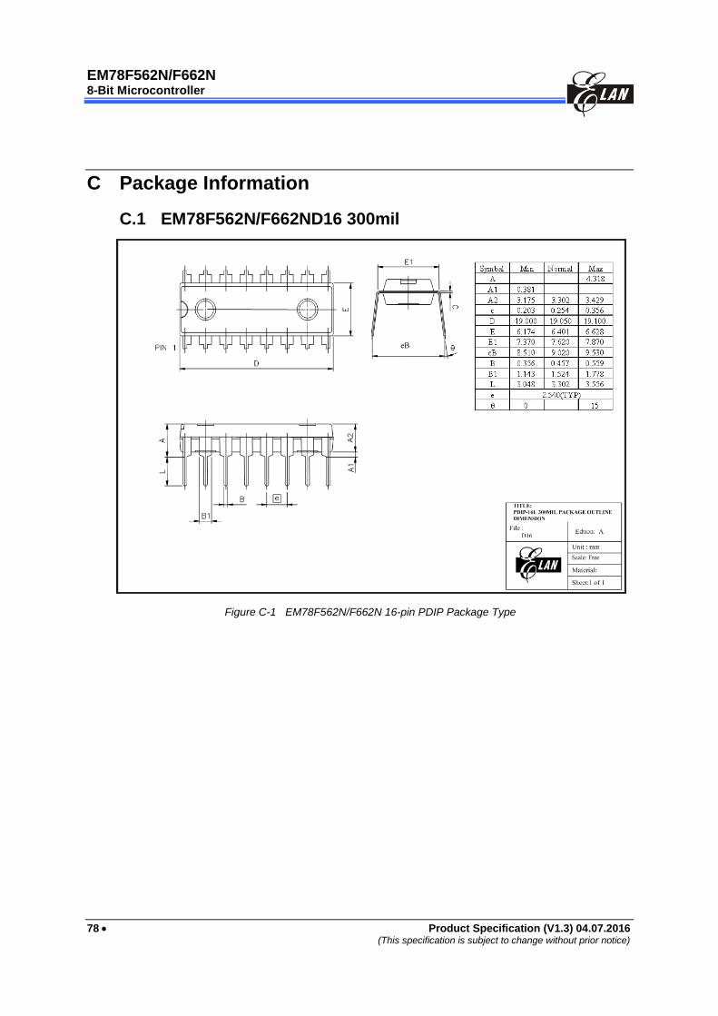
EM78F562N/F662N
8-Bit Microcontroller
78 Product Specification (V1.3) 04.07.2016
(This specification is subject to change without prior notice)
C Package Information
C.1 EM78F562N/F662ND16 300mil
Figure C-1 EM78F562N/F662N 16-pin PDIP Package Type
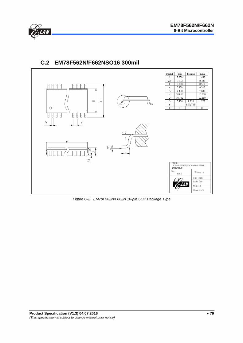
EM78F562N/F662N
8-Bit Microcontroller
Product Specification (V1.3) 04.07.2016 79 (This specification is subject to change without prior notice)
C.2 EM78F562N/F662NSO16 300mil
Figure C-2 EM78F562N/F662N 16-pin SOP Package Type
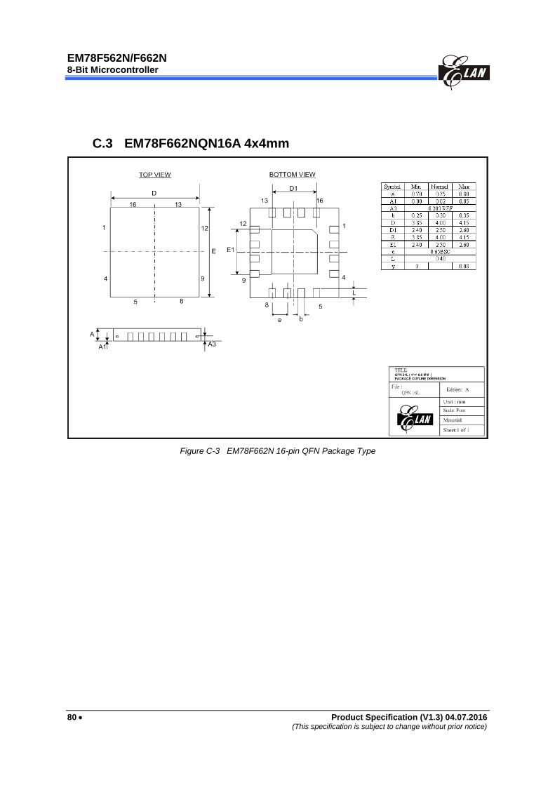
EM78F562N/F662N
8-Bit Microcontroller
80 Product Specification (V1.3) 04.07.2016
(This specification is subject to change without prior notice)
C.3 EM78F662NQN16A 4x4mm
Figure C-3 EM78F662N 16-pin QFN Package Type

EM78F562N/F662N
8-Bit Microcontroller
Product Specification (V1.3) 04.07.2016 81 (This specification is subject to change without prior notice)
C.4 EM78F662NSS16 150mil
TITLE:SSOP 16L (150MIL)PACKAGE OUTLINE DIMENSION
Unit : mm
Scale: Free
File : SSOP 16L
Material:
Edtion: A
Sheet:1 of 1
Package Type : SSOP-16L
Symbal Min Normal Max
A 1.35 1.63 1.75
A1 0.10 0.18 0.25
A2 - - 1.50
b 0.20 - 0.30
b1 0.20 0.25 0.28
c 0.18 - 0.25
c1 0.18 0.20 0.23
D 4.80 4.90 5.00
E 5.79 5.99 6.20
E1 3.81 3.91 3.99
L 0.41 0.64 1.27
e
θ 0° - 8°
.025BASIC
EMC(mm )
Figure C-4 EM78F662N 16-pin SSOP Package Type

EM78F562N/F662N
8-Bit Microcontroller
82 Product Specification (V1.3) 04.07.2016
(This specification is subject to change without prior notice)
C.5 EM78F562N/F662ND18 300mil
Min Normal Max
4.450
0.381
3.175 3.302 3.429
0.203 0.254 0.356
22.610 22.860 23.110
6.220 6.438 6.655
7.370 7.620 7.870
8.510 9.020 9.530
0.356 0.457 0.559
1.143 1.524 1.778
3.048 3.302 3.556
2.540(TYP)
0 15
Symbol
A
A1
A2
c
D
E1
E
eB
B
B1
L
e
θθ
eB
TITLE:PDIP-18L 300MIL PACKAGE OUTLINE DIMENSION
Unit : mm
Scale: Free
File : D18
Material:
Edtion: A
Sheet:1 of 1
Figure C-5 EM78F562N/F6622N 18-pin PDIP Package Type
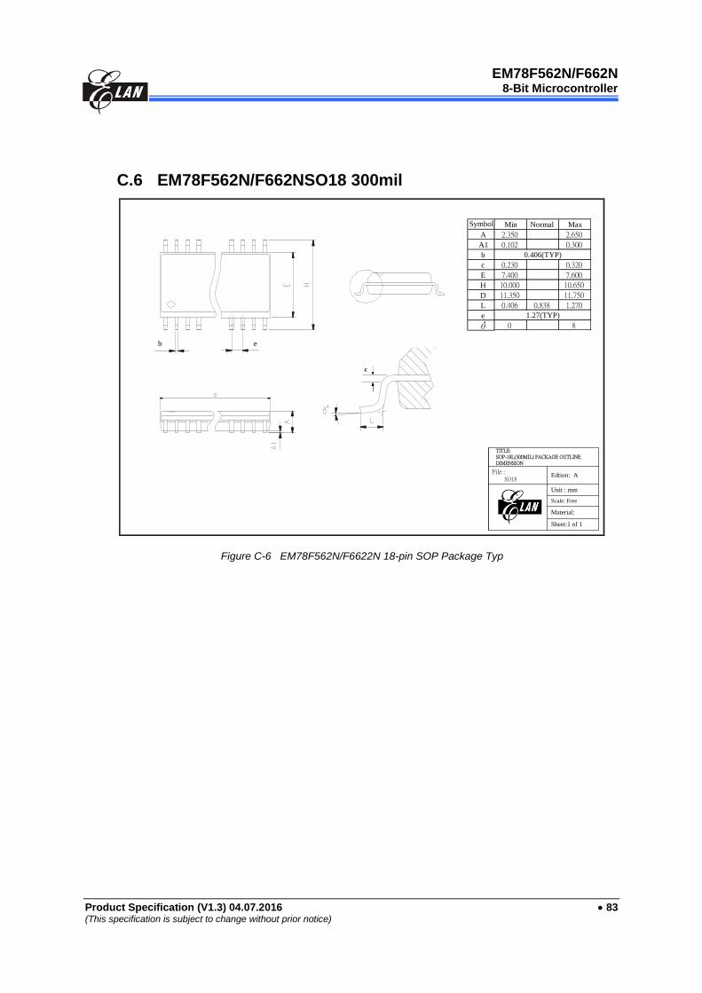
EM78F562N/F662N
8-Bit Microcontroller
Product Specification (V1.3) 04.07.2016 83 (This specification is subject to change without prior notice)
C.6 EM78F562N/F662NSO18 300mil
b e
Min Normal Max
2.350 2.650
0.102 0.300
0.406(TYP)
0.230 0.320
7.400 7.600
10.000 10.650
11.350 11.750
0.406 0.838 1.270
1.27(TYP)
0 8
Symbol
A
A1
b
c
E
H
D
L
e
θ
c
TITLE:SOP-18L(300MIL) PACKAGE OUTLINE DIMENSION
Unit : mm
Scale: Free
File : SO18
Material:
Edtion: A
Sheet:1 of 1
Figure C-6 EM78F562N/F6622N 18-pin SOP Package Typ

EM78F562N/F662N
8-Bit Microcontroller
84 Product Specification (V1.3) 04.07.2016
(This specification is subject to change without prior notice)
C.7 EM78F562N/F662ND20 300mil
TITLE:
PDIP-20L 300MIL PACKAGE
OUTLINE DIMENSION
Unit : mm
Scale: Free
File :
D20
Material:
Edtion: A
Sheet:1 of 1
Min Normal Max
4.450
0.381
3.175 3.302 3.429
0.203 0.254 0.356
25.883 26.060 26.237
6.220 6.438 6.655
7.370 7.620 7.870
8.510 9.020 9.530
0.356 0.457 0.559
1.143 1.524 1.778
3.048 3.302 3.556
2.540(TYP)
0 15
Symbol
A
A1
A2
c
D
E1
E
eB
B
B1
L
e
θ
A2
A1
E
Figure C-7 EM78F562N/F662N 20-pin PDIP Package Type

EM78F562N/F662N
8-Bit Microcontroller
Product Specification (V1.3) 04.07.2016 85 (This specification is subject to change without prior notice)
C.8 EM78F562/F662NSO20 300mil
TITLE:
SOP-20L(300MIL) PACKAGE
OUTLINE DIMENSION
Unit : mm
Scale: Free
File :
SO20
Material:
Edtion: A
Sheet:1 of 1
b e
Symbol
A
A1
b
c
E
H
D
L
e
θ
c
Min Normal Max
2.350 2.650
0.102 0.300
0.406(TYP)
0.230 0.320
7.400 7.600
10.000 10.650
12.600 12.900
0.630 0.838 1.100
1.27(TYP)
0 8
Figure C-8 EM78F562N/F662N 20-pin SOP Package Typ

EM78F562N/F662N
8-Bit Microcontroller
86 Product Specification (V1.3) 04.07.2016
(This specification is subject to change without prior notice)
D Quality Assurance and Reliability
Test Category Test Conditions Remarks
Solderability Solder temperature=2455°C, for 5 seconds up to the
stopper using a rosin-type flux –
Pre-condition
Step 1: TCT, 65°C (15mins)~150°C (15mins), 10 cycles
For SMD IC (such as
SOP, QFP, SOJ, etc)
Step 2: Bake at 125°C, TD (endurance)=24 hrs
Step 3: Soak at 30°C/60%, TD (endurance)=192 hrs
Step 4: IR flow 3 cycles
(Pkg thickness 2.5mm or
Pkg volume 350mm3 ----2255°C)
(Pkg thickness 2.5mm or
Pkg volume 350mm3 ----2405°C)
Temperature cycle
test -65°C (15mins)~150°C (15mins), 200 cycles –
Pressure cooker test TA =121°C, RH=100%, pressure=2 atm,
TD (endurance)= 96 hrs –
High temperature /
High humidity test TA=85°C , RH=85%, TD (endurance) = 168 , 500 hrs –
High-temperature
storage life TA=150°C, TD (endurance) = 500, 1000 hrs –
High-temperature
operating life
TA=125°C, VCC = Max. operating voltage,
TD (endurance) = 168, 500, 1000 hrs –
Latch-up TA=25°C, VCC = Max. operating voltage, 150mA/20V –
ESD (HBM) TA=25°C, ∣± 3KV∣ IP_ND,OP_ND,IO_ND
IP_NS,OP_NS,IO_NS
IP_PD,OP_PD,IO_PD,
IP_PS,OP_PS,IO_PS,
VDD-VSS(+),VDD_VSS
(-) mode
ESD (MM) TA=25°C, ∣± 300V∣
D.1 Address Trap Detect
An address trap detect is one of the MCU embedded fail-safe functions that detects
MCU malfunction caused by noise or the like. Whenever the MCU attempts to fetch an
instruction from a certain section of ROM, an internal recovery circuit is auto started. If
a noise-caused address error is detected, the MCU will repeat execution of the
program until the noise is eliminated. The MCU will then continue to execute the next
program.